WO2012017888A1 - 電子部品の製造方法および電子部品 - Google Patents
電子部品の製造方法および電子部品 Download PDFInfo
- Publication number
- WO2012017888A1 WO2012017888A1 PCT/JP2011/067071 JP2011067071W WO2012017888A1 WO 2012017888 A1 WO2012017888 A1 WO 2012017888A1 JP 2011067071 W JP2011067071 W JP 2011067071W WO 2012017888 A1 WO2012017888 A1 WO 2012017888A1
- Authority
- WO
- WIPO (PCT)
- Prior art keywords
- electronic component
- substrate
- metal lid
- layer
- metal
- Prior art date
Links
- 238000004519 manufacturing process Methods 0.000 title claims abstract description 62
- 239000002184 metal Substances 0.000 claims abstract description 209
- 229910052751 metal Inorganic materials 0.000 claims abstract description 209
- 239000000758 substrate Substances 0.000 claims abstract description 105
- 239000000463 material Substances 0.000 claims abstract description 55
- 238000005530 etching Methods 0.000 claims abstract description 10
- 238000000034 method Methods 0.000 claims description 44
- 239000011159 matrix material Substances 0.000 claims description 24
- 238000009736 wetting Methods 0.000 claims description 6
- 239000010410 layer Substances 0.000 description 158
- 238000007747 plating Methods 0.000 description 22
- 239000007864 aqueous solution Substances 0.000 description 12
- HEMHJVSKTPXQMS-UHFFFAOYSA-M Sodium hydroxide Chemical compound [OH-].[Na+] HEMHJVSKTPXQMS-UHFFFAOYSA-M 0.000 description 9
- 229910002058 ternary alloy Inorganic materials 0.000 description 9
- 238000009713 electroplating Methods 0.000 description 7
- 229910000679 solder Inorganic materials 0.000 description 5
- 238000010586 diagram Methods 0.000 description 4
- 238000005304 joining Methods 0.000 description 4
- 229910052759 nickel Inorganic materials 0.000 description 4
- 239000002253 acid Substances 0.000 description 3
- 229910045601 alloy Inorganic materials 0.000 description 3
- 239000000956 alloy Substances 0.000 description 3
- 239000000919 ceramic Substances 0.000 description 3
- 238000001035 drying Methods 0.000 description 3
- 238000004070 electrodeposition Methods 0.000 description 3
- 229910052737 gold Inorganic materials 0.000 description 3
- 230000001771 impaired effect Effects 0.000 description 3
- 238000012545 processing Methods 0.000 description 3
- 239000010453 quartz Substances 0.000 description 3
- VYPSYNLAJGMNEJ-UHFFFAOYSA-N silicon dioxide Inorganic materials O=[Si]=O VYPSYNLAJGMNEJ-UHFFFAOYSA-N 0.000 description 3
- 239000000243 solution Substances 0.000 description 3
- 229910020836 Sn-Ag Inorganic materials 0.000 description 2
- 229910020988 Sn—Ag Inorganic materials 0.000 description 2
- 239000000853 adhesive Substances 0.000 description 2
- 230000001070 adhesive effect Effects 0.000 description 2
- 239000004020 conductor Substances 0.000 description 2
- 238000007796 conventional method Methods 0.000 description 2
- 238000010438 heat treatment Methods 0.000 description 2
- 229910000833 kovar Inorganic materials 0.000 description 2
- CNQCVBJFEGMYDW-UHFFFAOYSA-N lawrencium atom Chemical compound [Lr] CNQCVBJFEGMYDW-UHFFFAOYSA-N 0.000 description 2
- 238000002844 melting Methods 0.000 description 2
- 230000008018 melting Effects 0.000 description 2
- 238000004544 sputter deposition Methods 0.000 description 2
- 238000007740 vapor deposition Methods 0.000 description 2
- 229910017398 Au—Ni Inorganic materials 0.000 description 1
- 229910015363 Au—Sn Inorganic materials 0.000 description 1
- 229910000906 Bronze Inorganic materials 0.000 description 1
- 229910021578 Iron(III) chloride Inorganic materials 0.000 description 1
- 229910001030 Iron–nickel alloy Inorganic materials 0.000 description 1
- OAICVXFJPJFONN-UHFFFAOYSA-N Phosphorus Chemical compound [P] OAICVXFJPJFONN-UHFFFAOYSA-N 0.000 description 1
- 239000003513 alkali Substances 0.000 description 1
- PNEYBMLMFCGWSK-UHFFFAOYSA-N aluminium oxide Inorganic materials [O-2].[O-2].[O-2].[Al+3].[Al+3] PNEYBMLMFCGWSK-UHFFFAOYSA-N 0.000 description 1
- QVGXLLKOCUKJST-UHFFFAOYSA-N atomic oxygen Chemical compound [O] QVGXLLKOCUKJST-UHFFFAOYSA-N 0.000 description 1
- 239000010974 bronze Substances 0.000 description 1
- 229910010293 ceramic material Inorganic materials 0.000 description 1
- 238000010276 construction Methods 0.000 description 1
- 229910052802 copper Inorganic materials 0.000 description 1
- KUNSUQLRTQLHQQ-UHFFFAOYSA-N copper tin Chemical compound [Cu].[Sn] KUNSUQLRTQLHQQ-UHFFFAOYSA-N 0.000 description 1
- 239000013078 crystal Substances 0.000 description 1
- 230000006378 damage Effects 0.000 description 1
- 230000003247 decreasing effect Effects 0.000 description 1
- 230000002542 deteriorative effect Effects 0.000 description 1
- 238000011161 development Methods 0.000 description 1
- 230000018109 developmental process Effects 0.000 description 1
- 238000010304 firing Methods 0.000 description 1
- 239000002241 glass-ceramic Substances 0.000 description 1
- 238000007654 immersion Methods 0.000 description 1
- 239000012535 impurity Substances 0.000 description 1
- 239000011229 interlayer Substances 0.000 description 1
- RBTARNINKXHZNM-UHFFFAOYSA-K iron trichloride Chemical compound Cl[Fe](Cl)Cl RBTARNINKXHZNM-UHFFFAOYSA-K 0.000 description 1
- 239000007788 liquid Substances 0.000 description 1
- 238000012986 modification Methods 0.000 description 1
- 230000004048 modification Effects 0.000 description 1
- 230000001590 oxidative effect Effects 0.000 description 1
- 229910052760 oxygen Inorganic materials 0.000 description 1
- 239000001301 oxygen Substances 0.000 description 1
- 238000000206 photolithography Methods 0.000 description 1
- 238000003825 pressing Methods 0.000 description 1
- 238000007639 printing Methods 0.000 description 1
- 230000011218 segmentation Effects 0.000 description 1
- 229910052709 silver Inorganic materials 0.000 description 1
- 238000001179 sorption measurement Methods 0.000 description 1
- 238000010897 surface acoustic wave method Methods 0.000 description 1
- 238000004381 surface treatment Methods 0.000 description 1
Images


Classifications
-
- H—ELECTRICITY
- H01—ELECTRIC ELEMENTS
- H01L—SEMICONDUCTOR DEVICES NOT COVERED BY CLASS H10
- H01L21/00—Processes or apparatus adapted for the manufacture or treatment of semiconductor or solid state devices or of parts thereof
- H01L21/02—Manufacture or treatment of semiconductor devices or of parts thereof
- H01L21/04—Manufacture or treatment of semiconductor devices or of parts thereof the devices having potential barriers, e.g. a PN junction, depletion layer or carrier concentration layer
- H01L21/50—Assembly of semiconductor devices using processes or apparatus not provided for in a single one of the subgroups H01L21/06 - H01L21/326, e.g. sealing of a cap to a base of a container
-
- H—ELECTRICITY
- H01—ELECTRIC ELEMENTS
- H01L—SEMICONDUCTOR DEVICES NOT COVERED BY CLASS H10
- H01L23/00—Details of semiconductor or other solid state devices
- H01L23/02—Containers; Seals
- H01L23/06—Containers; Seals characterised by the material of the container or its electrical properties
-
- H—ELECTRICITY
- H01—ELECTRIC ELEMENTS
- H01L—SEMICONDUCTOR DEVICES NOT COVERED BY CLASS H10
- H01L23/00—Details of semiconductor or other solid state devices
- H01L23/02—Containers; Seals
- H01L23/10—Containers; Seals characterised by the material or arrangement of seals between parts, e.g. between cap and base of the container or between leads and walls of the container
-
- H—ELECTRICITY
- H03—ELECTRONIC CIRCUITRY
- H03H—IMPEDANCE NETWORKS, e.g. RESONANT CIRCUITS; RESONATORS
- H03H9/00—Networks comprising electromechanical or electro-acoustic devices; Electromechanical resonators
- H03H9/02—Details
- H03H9/05—Holders; Supports
- H03H9/10—Mounting in enclosures
- H03H9/1007—Mounting in enclosures for bulk acoustic wave [BAW] devices
- H03H9/1014—Mounting in enclosures for bulk acoustic wave [BAW] devices the enclosure being defined by a frame built on a substrate and a cap, the frame having no mechanical contact with the BAW device
- H03H9/1021—Mounting in enclosures for bulk acoustic wave [BAW] devices the enclosure being defined by a frame built on a substrate and a cap, the frame having no mechanical contact with the BAW device the BAW device being of the cantilever type
-
- H—ELECTRICITY
- H01—ELECTRIC ELEMENTS
- H01L—SEMICONDUCTOR DEVICES NOT COVERED BY CLASS H10
- H01L2924/00—Indexing scheme for arrangements or methods for connecting or disconnecting semiconductor or solid-state bodies as covered by H01L24/00
- H01L2924/0001—Technical content checked by a classifier
- H01L2924/0002—Not covered by any one of groups H01L24/00, H01L24/00 and H01L2224/00
-
- H—ELECTRICITY
- H01—ELECTRIC ELEMENTS
- H01L—SEMICONDUCTOR DEVICES NOT COVERED BY CLASS H10
- H01L2924/00—Indexing scheme for arrangements or methods for connecting or disconnecting semiconductor or solid-state bodies as covered by H01L24/00
- H01L2924/095—Indexing scheme for arrangements or methods for connecting or disconnecting semiconductor or solid-state bodies as covered by H01L24/00 with a principal constituent of the material being a combination of two or more materials provided in the groups H01L2924/013 - H01L2924/0715
- H01L2924/097—Glass-ceramics, e.g. devitrified glass
- H01L2924/09701—Low temperature co-fired ceramic [LTCC]
-
- H—ELECTRICITY
- H01—ELECTRIC ELEMENTS
- H01L—SEMICONDUCTOR DEVICES NOT COVERED BY CLASS H10
- H01L2924/00—Indexing scheme for arrangements or methods for connecting or disconnecting semiconductor or solid-state bodies as covered by H01L24/00
- H01L2924/15—Details of package parts other than the semiconductor or other solid state devices to be connected
- H01L2924/161—Cap
- H01L2924/1615—Shape
- H01L2924/16152—Cap comprising a cavity for hosting the device, e.g. U-shaped cap
Definitions
- the present invention relates to a method of manufacturing an electronic component in which an electronic component element is accommodated in a space formed by a substrate and a metal lid. More specifically, the surface of the metal lid that contacts the substrate is highly flat and airtight.
- the present invention relates to a method for manufacturing an excellent electronic component.
- the electronic component element is hermetically sealed in a package in order to protect the electronic component element (electronic component main body) from the external environment.
- Patent Document 1 Japanese Patent Application Laid-Open No. 2005-159258
- a substrate assembly 102 in which a plurality of substrates 101 are formed in a matrix is prepared.
- the electronic component element (quartz vibration element) 103 is mounted on the metal lid assembly 105, and a plurality of metal lids 104 are formed in a matrix to prepare a metal lid assembly 105.
- the metal lid assembly 105 is bonded to the substrate assembly 102 using the bonding material 106 to form the electronic component assembly 107.
- FIG. A method of manufacturing an electronic component that is divided into electronic components (quartz crystal resonators) 108 is disclosed.
- the metal lid 104 (metal lid assembly 105) is made of, for example, a metal plate such as 42 alloy, Kovar, phosphor bronze, etc., and has a thickness of about 60 ⁇ m to 100 ⁇ m, and accommodates the electronic component element 103 by sheet metal processing.
- a recess 104a and a leg 104b are formed.
- the substrate 101 (substrate assembly 102) is made of, for example, a ceramic material such as glass ceramics or alumina ceramics, and a land electrode 101a for mounting the electronic component element 103 and a metal lid 104 are bonded to one main surface.
- a ceramic material such as glass ceramics or alumina ceramics
- a land electrode 101a for mounting the electronic component element 103 and a metal lid 104 are bonded to one main surface.
- an annular bonding electrode 101b is formed.
- the bonding material 106 is made of, for example, Au—Ni, Au—Sn, and the like, provided on the bonding electrode 101b of each substrate 101, heated to 300 ° C. to 350 ° C., melted, and bonded to the bonding electrode 101b and the metal lid. 104 legs 104b are joined.
- the metal lid 104 (metal lid assembly 105) is processed by sheet metal processing on a metal plate, and the substrate 101 and the concave portion 104a for accommodating the electronic component 103 are provided. Therefore, there is a problem in that the flatness of the surface of the leg 104b that comes into contact with the substrate 101a is low, and the airtightness after bonding to the substrate 101a is low. That is, even when a flat metal plate is used, when the recess 104a and the leg 104b are formed by pressing or the like, the flatness of the bottom surface of the leg 104b is impaired, and airtight leakage may occur after joining. was there.
- the width of the bottom surface of the leg portion 104b has to be increased, and there has been a problem that the electronic component is increased in size.
- the method of manufacturing an electronic component according to the present invention includes a step of preparing a substrate, a step of mounting an electronic component element on the substrate, and a recess formed on one main surface leaving an annular leg around the periphery.
- a step of bonding the metal lid to the substrate using a bonding material by application, and the concave portion of the metal lid is formed by etching a flat metal plate.
- a plurality of electronic components are collectively manufactured using a substrate assembly in which a plurality of substrates are formed in a matrix and a metal lid assembly in which a plurality of metal lids are formed in a matrix. It can also be applied to the case of manufacturing. That is, one embodiment of the method for manufacturing an electronic component according to the present invention includes a step of preparing a substrate assembly in which a plurality of substrates are formed in a matrix, and mounting an electronic component element on each of the plurality of substrates.
- a metal lid assembly in which a plurality of metal lids are formed in a matrix shape, with a recess formed on one main surface, leaving an annular leg around the periphery, and a bonding material supplied to the tip of the leg
- the assembly includes a step of joining the assembly to the substrate assembly to form an electronic component assembly, and a step of dividing the electronic component assembly into individual electronic components, and each recess of the plurality of metal lids is flat.
- a special metal plate It was to be formed by doing this.
- the electronic component manufacturing method of the present invention has the above-described configuration, that is, a flat metal plate is used for the metal lid, and the concave portion of the metal lid is formed by etching instead of sheet metal processing, the periphery of the concave portion
- the flatness of the end surface of the leg portion that is annularly formed and in contact with the substrate is not impaired during the manufacturing process. Therefore, the electronic component manufactured according to the present invention is excellent in airtightness. Further, even if the width of the end surface of the leg portion is reduced, the airtightness is not lowered. Therefore, the width of the end surface of the leg portion can be reduced, and the electronic component can be downsized.
- a joining material only to the end surface of the leg part of a metal lid.
- the bonding material does not become excessive, and the characteristic of the electronic component may deteriorate due to the excessive bonding material adhering to the electronic component element. Absent.
- a joint material accommodating portion may be formed on the end surface of the leg portion of the metal lid.
- the surplus joining material can be accommodated in the accommodating portion, and the surplus joining material adheres to the electronic component element. Can be prevented from deteriorating.
- an unwetting layer may be formed on the inner wall of the concave portion of the metal lid.
- the excess bonding material does not spread out on the inner wall of the concave portion of the metal lid, and drops from there and adheres to the electronic component element. The characteristics of electronic parts are not deteriorated. Further, since the bonding material does not wet and spread in the concave portion of the metal lid, the supply amount of the bonding material can be reduced from the beginning, and the material cost can be reduced.
- a lid electrode composed of a first layer containing Ni as a main component and a second layer containing Au as a main component is formed on the end surface of the leg portion of the metal lid, and Bi is mainly formed on the lid electrode.
- a bonding electrode composed of a first layer containing Ni as a main component and a second layer containing Au as a main component is formed on the portion of the substrate that contacts the metal lid. Then, the lid electrode and the bonding electrode may be bonded with a bonding material. In this case, Au and Ni are diffused from the lid electrode and the bonding electrode to form a Bi—Ni—Au ternary alloy in the bonding material containing Bi as a main component.
- the metal lid can be bonded to the substrate in a short time.
- the Bi-Ni-Au ternary alloy has a high melting point and is 400 ° C. or higher. Therefore, when the manufactured electronic component is mounted by reflow, it does not remelt and the metal lid comes off the substrate. There is no.
- the electronic parts to be manufactured have the same shape and size of the substrate and the shape and size of the metal lid as viewed in the plane direction.
- the area of the top surface of the metal lid can be maximized, and when the electronic component is held and mounted by vacuum suction, it can be reliably sucked.
- FIGS. 1A to 1C are cross-sectional views showing respective steps applied in the method for manufacturing an electronic component according to the first embodiment of the present invention.
- FIGS. 2D to 2F are sectional views showing respective steps applied in the method of manufacturing an electronic component according to the first embodiment of the present invention.
- 3 (G) to (I) are cross-sectional views showing respective steps applied in the method of manufacturing an electronic component according to the first embodiment of the present invention.
- 4 (J) to (L) are cross-sectional views showing respective steps applied in the method of manufacturing an electronic component according to the first embodiment of the present invention.
- 4 (M) to (O) are cross-sectional views showing respective steps applied in the method of manufacturing an electronic component according to the first embodiment of the present invention.
- FIGS. 11D to 11F are sectional views showing respective steps applied in the electronic component manufacturing method according to the fifth embodiment of the present invention.
- FIG. 12 (G) to (I) are cross-sectional views showing respective steps applied in the electronic component manufacturing method according to the fifth embodiment of the present invention.
- FIG. 13 (J) and FIG. 13 (K) are sectional views showing respective steps applied in the method for manufacturing an electronic component according to the fifth embodiment of the present invention.
- 14 (L) and 14 (M) are sectional views showing respective steps applied in the method for manufacturing an electronic component according to the fifth embodiment of the present invention.
- FIG. 15N is a cross-sectional view showing each step applied in the method for manufacturing an electronic component according to the fifth embodiment of the present invention.
- 16A to 16C are cross-sectional views showing respective steps applied in the method for manufacturing an electronic component according to the sixth embodiment of the present invention.
- FIG. 17D is a cross-sectional view showing each step applied in the method for manufacturing an electronic component according to the sixth embodiment of the present invention.
- 18A to 18C are cross-sectional views showing respective steps applied in the conventional method of manufacturing an electronic component.
- FIG. 1A to FIG. 5O are cross-sectional views showing respective steps applied in the method of manufacturing an electronic component according to the first embodiment of the present invention.
- a metal lid assembly in which a plurality of metal lids are formed in a matrix and a substrate assembly in which a plurality of substrates are formed in a matrix are prepared. After joining to form an electronic component assembly, the electronic component assembly is divided into individual electronic components.
- the metal lid assembly will be described first, and then the substrate assembly will be described.
- FIG. 1A shows a metal plate 1 used for manufacturing a metal lid assembly.
- a metal plate having a high flatness is used.
- a rolled plate is used as the metal plate, and the flatness is 5 ⁇ m or less.
- the material of the metal plate 1 is not particularly limited.
- an Fe—Ni alloy such as Kovar or 42 alloy can be used.
- the thickness of the metal plate 1 is the same as the height of the metal lid to be manufactured.
- the size (vertical, horizontal) of the metal plate 1 is determined in consideration of the size and number of metal lids to be manufactured.
- resists 2a and 2b are formed on both main surfaces of the metal plate 1, respectively.
- the resist 2a is formed on the entire surface of one main surface (upper side in the drawing) of the metal plate 1.
- the resist 2b is partially formed by providing a plurality of openings (portions where no resist is formed) 2c on the other main surface (lower side in the figure) of the metal plate 1.
- the shape and size (vertical and horizontal) of the opening 2c are the same as the shape and size of the recess formed in the metal lid to be manufactured.
- the openings 2c are formed in a matrix in the first resist 2b.
- a dry film resist is attached to both main surfaces of the metal plate 1.
- the dry film resist is exposed and developed by a commonly used photolithography process to form a resist 2a on one entire main surface of the metal plate 1 and a plurality of openings 2c on the other main surface. Obtained resist 2b is obtained.
- the resist 2a formed on one main surface of the metal plate 1 is also provided with, for example, a lattice-like opening, and a dicing groove for subsequent division is formed on the surface of the metal plate 1.
- the dry film resist those commercially available can be used. This dry film resist can be peeled off with an alkaline aqueous solution such as NaOH.
- the metal plate 1 exposed from the opening 2c is etched using, for example, an etching solution such as ferric chloride, and the other main surface of the metal plate 1 is etched.
- a plurality of recesses (recesses of the metal lid to be manufactured) 3 are formed.
- the depth of the recess 3 can be appropriately determined according to the height of the electronic component element to be accommodated, but in the present embodiment, the depth is set to 100 ⁇ m.
- the recess 3 may be formed by a dry process instead of the wet process as described above.
- the recessed part 3 is formed by an etching process, the flatness of the main surface at the side in which the recessed part 3 of the metal plate 1 was formed is not impaired in the middle of manufacture.
- the resists 2a and 2b are stripped from both main surfaces of the metal plate 1 using, for example, an alkaline aqueous solution such as NaOH.
- a plating mask sheet 5 is attached to one main surface of the metal plate 1.
- the plating mask sheet 5 those that are widely available on the market can be used.
- a Ni layer (first layer of the lid electrode) 6 made of a material mainly composed of Ni is formed on the metal plate 1 by a general electrolytic plating method. To do. Since the plating mask sheet 5 is adhered to one main surface of the metal plate 1, the Ni layer 6 is not formed. On the other main surface of the metal plate 1, the Ni layer 6 is formed including the inner wall of the recess 3.
- the thickness of the Ni layer 6 is not particularly limited, but is set to 1 to 5 ⁇ m in this embodiment.
- an Au layer (lid) made of a material mainly composed of Au is formed on the Ni layer (first layer of the lid electrode) 6 by a general electrolytic plating method. (Second layer of electrode) 7 is formed. Since the plating mask sheet 5 is adhered to one main surface of the metal plate 1, the Au layer 7 is not formed. An Au layer 7 including the inner wall of the recess 3 is formed on the other main surface of the metal plate 1.
- the thickness of the Au layer 7 is not particularly limited, but in the present embodiment, it is 0.1 to 1.0 ⁇ m.
- a Bi layer (bonding) made of a material containing Bi as a main component is formed on the Au layer (second layer of the lid electrode) 7 by a general electrolytic plating method.
- Material layer) 8 is formed. Since the plating mask sheet 5 is adhered to one main surface of the metal plate 1, the Bi layer 8 is not formed.
- a Bi layer 8 including the inner wall of the recess 3 is formed on the other main surface of the metal plate 1.
- the thickness of the Bi layer 8 is not particularly limited, but is 10 ⁇ m in this embodiment.
- the Ni layer (first layer of the lid electrode) 6, the Au layer (second layer of the lid electrode) 7, and the Bi layer (bonding material layer) 8 are all formed.
- the Ni layer 6 and the Au layer 7 may be formed by vapor deposition or sputtering
- the Bi layer 8 may be formed by vapor deposition, sputtering or printing.
- Sn—Ag solder or AuSn solder may be used as the bonding material instead of the Bi layer 8 which is the bonding material layer.
- the plating mask sheet 5 is peeled from one main surface of the metal plate 1.
- the plating mask sheet 5 is peeled off, for example, by gripping and peeling the end of the plating mask sheet 5 with a jig.
- Each metal lid 9 has a concave portion 9a (3) formed at the center of the other main surface, and an annular shape around the concave portion 9a.
- Legs 9b are formed.
- a Ni layer (first layer of the lid electrode) 6, an Au layer (second layer of the lid electrode) 7, and a Bi layer (bonding material layer) 8 are sequentially formed. Is formed.
- FIG. 4J shows a substrate assembly 12 in which a plurality of substrates 11 are formed in a matrix.
- the substrate 11 (substrate assembly 12) is made of, for example, a multilayer ceramic substrate, and the above-described metal lid 9 ( The first layer for bonding the metal lid assembly 10) is the Ni layer 13a as the first layer, the Au layer 14a as the second layer, and the Ni layer 13b as the first layer for mounting the electronic component element,
- the second layer is formed with a land electrode made of the Au layer 14b.
- the joining electrode is formed in an annular shape corresponding to the leg portion 9 b of the metal lid 9.
- the junction electrode and the land electrode are respectively connected to the terminal electrode 11b formed on the other main surface of the substrate 11 via the wiring 11a formed of the via conductor and the interlayer conductor formed inside the substrate 11. Yes.
- the material of the wiring 11a and the terminal electrode 11b is not particularly limited. For example, Cu, Ag, Ni, or the like can be used as the main component. In the completed electronic component, if the terminal electrode 11b to which the bonding electrode is connected is grounded, the metal lid 9 bonded to the bonding electrode can be grounded.
- the substrate 11 (substrate assembly 12) can be manufactured, for example, by the following method. That is, first, a plurality of ceramic green sheets are prepared, a conductive paste is applied to the surface of a predetermined green sheet, a conductive paste is filled in the vias, the green sheets are laminated in a predetermined order, and added. The substrate 11 on which the wiring 11a, the terminal electrode 11b, the first Ni layer 13a of the bonding electrode, and the first Ni layer 13b of the land electrode are formed is obtained. Subsequently, the second Au layer 14a of the bonding electrode is formed on the Ni layer 13a, and the second Au layer 14b of the land electrode is formed on the Ni layer 13b by a method such as electrolytic plating.
- the substrate 11 is completed.
- the first Ni layer 13a of the bonding electrode and the first Ni layer 13b of the land electrode were obtained by firing, but a Ni layer was formed on the 13a and 13b by plating.
- An Au layer may be formed thereon.
- the electronic component element 16 is mounted on the land electrode (Ni layer 13b, Au layer 14b) of each substrate 11 using, for example, a conductive adhesive 15.
- a piezoelectric element is used as the electronic component element 16.
- the electronic component element (piezoelectric element) 16 is made of a piezoelectric material such as quartz and is not shown, but is polarized and has a plurality of electrodes formed on its surface. When a predetermined voltage is applied between the electrodes, a predetermined frequency is applied. Vibrates and functions as an oscillator, for example.
- the electronic component element (piezoelectric element) 16 needs to be hermetically sealed in the package and protected from the external environment because the vibration frequency may fluctuate when moisture is absorbed.
- the metal lid assembly 10 is placed on the substrate assembly 12. At this time, alignment is performed so that the metal lids 9 are arranged on the respective substrates 11.
- the substrate assembly 12 and the metal lid assembly 10 placed on the substrate assembly 12 are sandwiched by bonding tools 17a and 17b from above and below, for example, 1 Pressurized at a pressure of 5 to 20 MPa for 10 minutes and heated at 250 to 350 ° C. to melt the Bi layer (bonding material layer) 8, and a Ni layer formed on the end face of the leg 9 b of the metal lid 9 ( (First layer of lid electrode) 6, Au layer (second layer of lid electrode) 7, Ni layer 13a (first layer of bonding electrode) formed on substrate 11, Au layer 14a (first layer of bonding electrode) From the second layer), Au and Ni are diffused into the Bi layer (bonding material layer) 8.
- a Bi—Ni—Au ternary alloy layer 18 is formed, the metal lid assembly 10 is joined to the substrate assembly 12, and a plurality of electronic components 19 are arranged in a matrix.
- the assembled electronic component assembly 20 is formed.
- the Bi—Ni—Au ternary alloy layer 18 has a melting point of 400 ° C. or higher, the electronic component manufactured by the manufacturing method of the present embodiment is remelted even when it is heated when mounted with reflow solder or the like. And a highly reliable joint can be obtained.
- Sn—Ag solder or AuSn solder can be used as the bonding material instead of the Bi layer 8 as the bonding material layer. In this case as well, bonding is performed by the same pressure and heating process. be able to.
- Bi is used for the bonding material, it is possible to obtain a bond that is less expensive and more difficult to remelt.
- the electronic component assembly 20 in which a plurality of electronic components 19 are arranged in a matrix is diced by an XX portion, a YY portion, a ZZ portion, etc., indicated by chain lines in FIG.
- Each electronic component (piezoelectric vibrator) 19 is obtained by dividing by a method such as the above.
- the metal lid 9 is firmly bonded to the substrate 11 by the Bi—Ni—Au ternary alloy layer 18. If the connection terminal 11 b connected to the Bi—Ni—Au ternary alloy layer 18 is grounded, the inside of the recess 9 b of the metal lid 9 can be well shielded by the metal lid 9.
- the completed electronic component 19 has the same shape and size of the substrate 11 and the same shape and size of the metal lid 19 as viewed in the plane direction. Therefore, the electronic component 19 has the maximum area of the top surface of the metal lid 19, and can be reliably adsorbed when being held and mounted by vacuum adsorption.
- the Ni layer 6 and the Au layer 7 as the lid electrode and the Bi layer 8 as the bonding material layer are formed on the end surface of the leg portion 9a of the lid electrode 9 on one main surface of the substrate 11.
- the Ni layer 13a and the Au layer 14a are formed as the bonding electrodes.
- the type, the number of layers, the thickness, etc. are arbitrary. For example, other materials may be used or the number of layers may be increased or decreased. Can do.
- a piezoelectric vibrator is manufactured as an electronic component.
- the manufactured electronic component is not limited to a piezoelectric vibrator, and may be another electronic component such as a gyroscope or a surface acoustic wave device. May be.
- FIGSecond Embodiment 6A to 6C are process diagrams showing each process applied in the method for manufacturing an electronic component according to the second embodiment of the present invention.
- the electronic component manufacturing method according to the second embodiment is obtained by changing a part of the steps of the electronic component manufacturing method according to the first embodiment shown in FIGS. 1 (A) to 5 (O). .
- the electronic component manufacturing method according to the second embodiment is the same as that shown in FIG. 1C until the plurality of recesses 3 are formed on the other main surface of the metal plate 1 by etching, for example.
- the same process as in one embodiment is used.
- the resist 2b formed on the other main surface is peeled off from the metal plate 1. That is, the resist 2a formed on one main surface (upper side in the drawing) of the metal substrate 1 does not peel off.
- this step for example, only the other main surface of the metal substrate 1 is immersed in an alkaline aqueous solution, or the resist 2a formed on one main surface of the metal substrate 1 is masked, and then the metal substrate 1 is alkali aqueous solution. It can be performed by a method such as immersion in
- an Ni layer (first layer of the lid electrode) 6 an Au layer (second layer of the lid electrode) 7, Bi
- the layer (bonding material layer) 8 is formed in order by electrolytic plating. Since the resist 2a is formed on one main surface of the metal plate 1, the Ni layer 6, the Au layer 7, and the Bi layer 8 are not formed.
- a recess 9a (3) is formed in the center, and the periphery of the recess 9a.
- An annular leg portion 9b is formed, and a metal lid assembly 10 in which a plurality of metal lids 9 are formed in a matrix is completed.
- the one main surface of the metal plate 1 is resist 2a. So that they are not formed. Therefore, in this embodiment, use of the plating mask sheet 5 used in the first embodiment can be omitted.
- FIGS. 7A to 8E are process diagrams showing each process applied in the method of manufacturing an electronic component according to the third embodiment of the present invention.
- the electronic component manufacturing method according to the third embodiment is obtained by changing a part of the steps of the electronic component manufacturing method according to the first embodiment shown in FIGS. 1 (A) to 5 (O). .
- the electronic component manufacturing method according to the third embodiment is the same as that shown in FIG. 1C until the plurality of recesses 3 are formed on the other main surface of the metal plate 1 by etching, for example.
- the same process as in one embodiment is used.
- a second resist 22 is formed on the inner wall of the recess 3 as shown in FIG.
- the second resist 22 is formed of an electrodeposition resist.
- the entire metal plate 1 is immersed in an acid-based surface treatment solution, and the inner wall of the recess 3 is degreased and cleaned.
- the entire metal plate 1 is immersed in a trade name “Elecoat EU-XC” manufactured by Shimizu Corporation at a liquid temperature of 40 ° C., and a current of DC 100 V is set to 30 with the metal plate 1 as a cathode, the SUS plate as an anode.
- a current is applied for 2 seconds, and an electrodeposition resist film having a thickness of about 10 ⁇ m is formed on the inner wall of the recess 3.
- drying, exposure, and development are performed to obtain a second resist 22 on the inner wall of the recess 3.
- the second resist 22 is peeled off with an acid aqueous solution, but is not peeled off with an alkaline aqueous solution.
- the resists 2a and 2b are stripped from both main surfaces of the metal substrate 1 using, for example, an alkaline aqueous solution such as NaOH.
- an alkaline aqueous solution such as NaOH.
- the second resist 22 does not peel off with the alkaline aqueous solution and remains.
- a plating mask sheet 5 is attached to one main surface of the metal plate 1.
- the plating mask sheet 5 those that are widely available on the market can be used.
- the Ni layer (first layer of the lid electrode) 26, the Au layer (second layer of the lid electrode) 27, the Bi layer (bonding material layer) are formed on the metal plate 1.
- ) 28 are sequentially formed by electrolytic plating. Since the plating mask sheet 5 is formed on one main surface of the metal plate 1, the Ni layer 26, the Au layer 27, and the Bi layer 28 are not formed. Further, since the second resist 22 is also formed on the inner wall of the recess 3 formed on the other main surface of the metal plate 1, the Ni layer 26, the Au layer 27, and the Bi layer 28 are not formed.
- the plating mask sheet 5 is peeled off from one main surface of the metal plate 1 and the second resist 22 is peeled off from the inner wall of the recess 3. Either the peeling of the plating mask sheet 5 or the peeling of the second resist 4 may be performed first.
- the plating mask sheet 5 is peeled off, for example, by gripping and peeling the end of the plating mask sheet 5 with a jig.
- the second resist 22 is removed using an acid aqueous solution, for example, “DLP-42” manufactured by Shimizu.
- the second resist 22 is not necessarily peeled off and may remain in the recess 3.
- a concave portion 9a (3) is formed at the center, an annular leg portion 9b is formed around the concave portion 9a, and a metal lid assembly 10 in which a plurality of metal lids 9 are formed in a matrix is completed.
- the Ni layer 26, the Au layer 27, and the Bi layer 28 are formed only on the end surface of the leg 9b of the metal lid 9, and the inner wall of the recess 9 (3) of the metal lid 9 is formed. In order not to form these.
- the Bi of the Bi layer 28 that is a bonding material is not excessive, and the excessive bonding material is an electronic component element. The characteristic of the electronic component is not deteriorated due to adhesion to 16 or the like.
- FIG. 9A is a process diagram showing processes applied in the method for manufacturing an electronic component according to the fourth embodiment of the present invention.
- the electronic component manufacturing method according to the fourth embodiment is obtained by changing a part of the steps of the electronic component manufacturing method according to the third embodiment shown in FIGS. 7 (A) to 8 (E). .
- the plating mask sheet 5 is shown from one main surface of the metal plate 1 and the second wall is shown from the inner wall of the recess 9a (3) as shown in FIG. Up to the point where the resist 22 is peeled off, the same process as in the third embodiment is used.
- the non-wetting layer 23 is formed again on the inner wall of the recess 9a (3) from which the second resist 22 has been peeled off.
- the non-wetting layer 23 is formed, for example, by oxidizing the portion exposed on the inner wall of the recess 9a (3) of the metal plate 1 by a dry process using oxygen plasma.
- an inorganic film or an organic film having poor wettability may be formed separately.
- the second resist 22 formed on the inner wall of the recess 9 a (3) of the metal plate 1 may be left without being peeled to form the non-wetting layer 23.
- the non-wetting layer 23 is formed on the inner wall of the recess 9 a (3) of the metal lid 9.
- the recesses 9a (3) of the metal lid 9 are formed.
- the inner wall does not spread out and drops from there and adheres to the electronic component element 16 so that the characteristics of the electronic component do not deteriorate.
- FIGS. 10A to 15M are cross-sectional views showing respective steps applied in the method for manufacturing an electronic component according to the fifth embodiment of the present invention.
- a metal plate 31 used for manufacturing a metal lid assembly is prepared.
- resists 32a and 32b are formed on both main surfaces of the metal plate 31, respectively.
- the resist 32 a is formed on the entire surface of one main surface (upper side in the drawing) of the metal plate 31.
- the resist 32 b is partially formed by providing a plurality of openings 32 c on the other main surface (lower side in the figure) of the metal plate 31.
- the metal plate 31 exposed from the opening 32c was etched using an etching solution, and a plurality of surpluses were formed on the other main surface of the metal plate 31.
- a housing portion 33 for housing the bonding material is formed.
- the resists 32a and 32b are stripped from both main surfaces of the metal plate 31 using an alkaline aqueous solution.
- resists 42a and 42b are formed again on both main surfaces of the metal plate 31, respectively.
- the resist 42 a is formed on the entire surface of one main surface (upper side in the drawing) of the metal plate 31.
- the resist 42b is partially formed by providing a plurality of openings 42c on the other main surface (lower side in the figure) of the metal plate 31.
- the resist 42b is formed so as to close the housing portion 33 formed on the metal plate 31 previously.
- the metal plate 31 exposed from the opening 42c is etched using an etchant so that the electronic component element is accommodated on the other main surface of the metal plate 31.
- the recess 43 is formed.
- a second resist 52 is formed on the inner wall of the recess 43 by an electrodeposition resist.
- the resists 42a and 42b are peeled off from both main surfaces of the metal plate 31 using an alkaline aqueous solution.
- a plating mask sheet 35 is attached to one main surface of the metal plate 31.
- a Ni layer (first layer of the lid electrode) 36, an Au layer (second layer of the lid electrode) 37, a Bi layer (bonding material layer) are formed on the metal plate 31. 38) are formed in this order by electrolytic plating.
- the Ni layer 36, the Au layer 37, and the Bi layer 38 are not formed on the inner wall of the recess 43 because the second resist 52 is formed, but are formed on the inner wall of the housing portion 43.
- the plating mask sheet 35 is peeled off from one main surface of the metal plate 31 and the second resist 52 is peeled off from the inner wall of the recess 43 to form a plurality of metal lids.
- a metal lid assembly 40 having a matrix 39 formed in a matrix is completed, and this is placed on the substrate assembly 12 in which a plurality of substrates 11 are formed in a matrix.
- the substrate assembly 12 and the metal lid assembly 40 placed on the substrate assembly 12 are sandwiched by the bonding tools 17a and 17b from above and below, and pressed.
- the Bi layer 38 is melted, and the Ni layer 36 and Au layer 37 formed on the end surface of the leg portion 39b of the metal lid 39 and the Ni layer 13a and Au layer 14a formed on the substrate 11 are Au and Ni are diffused into the layer 38.
- a Bi—Ni—Au ternary alloy layer 48 is formed, the metal lid assembly 10 is bonded to the substrate assembly 12, and a plurality of electronic components 49 are arranged in a matrix.
- the assembled electronic component assembly 50 is formed.
- the surplus Bi—Ni—Au ternary alloy layer 48 is accommodated in the accommodating portion 33 formed in the metal lid 39, so that it does not flow to the concave portion 39 a (43) side of the metal lid 39.
- the electronic component element 16 does not adhere.
- an electronic component assembly 50 in which a plurality of electronic components 49 are arranged in a matrix is divided into SS portions, TT portions, etc., indicated by chain lines in FIG. As shown in N), individual electronic components 49 are obtained.
- the accommodating portion 33 is formed on the leg portion 39b of the metal lid 39, and Bi of the Bi layer 38, which is a surplus bonding material, is accommodated when the substrate 11 and the metal lid 39 are joined. Since it is accommodated in the part 33, Bi does not adhere to the electronic component element 16, and the characteristics of the electronic component do not deteriorate.
- FIG. 16A to FIG. 17D are process diagrams showing each process applied in the electronic component manufacturing method according to the sixth embodiment of the present invention.
- the electronic component manufacturing method according to the sixth embodiment is obtained by changing a part of the steps of the electronic component manufacturing method according to the first embodiment shown in FIGS. 1 (A) to 5 (O). .
- the manufacturing method of the electronic component according to the sixth embodiment includes the steps up to manufacturing the metal lid assembly 10 in which a plurality of metal lids 9 are formed in a matrix shape as shown in FIG. 4 (K), the same process as that of the first embodiment is performed until the substrate assembly 12 in which the plurality of substrates 11 are formed in a matrix shape and the electronic component element 16 is mounted on each substrate 11. Use.
- the metal lid assembly 10 is divided into individual metal lids 9 and attached to a metal jig 51a.
- the sticking is performed via a rubber sheet having tackiness that is installed on the surface of a metal jig 51a.
- the board assembly 12 on which the electronic component elements 16 are mounted is divided into individual boards 11 and similarly attached to a metal jig 51b.
- the metal lid 9 attached to the jig 51a is placed on the substrate 11 attached to the jig 51b.
- a plurality of substrates 11 are adhered to the jig 51b, and a plurality of metal lids 9 are adhered to the jig 51a, and this step is performed in a lump.
- the metal lid assembly 10 is not divided into the individual electronic components 19 after the metal lid assembly 10 and the substrate assembly 12 are joined.
- the present invention can also be implemented in the form of dividing the metal lid 9, dividing the substrate assembly 12 into individual substrates 11, and bonding the metal lid 9 and the substrate 11. Thereby, destruction of the electronic component element 16 by the load at the time of a division
- the present construction method can be applied to an aggregate substrate with poor dimensional accuracy.
Landscapes
- Physics & Mathematics (AREA)
- Engineering & Computer Science (AREA)
- Condensed Matter Physics & Semiconductors (AREA)
- General Physics & Mathematics (AREA)
- Computer Hardware Design (AREA)
- Microelectronics & Electronic Packaging (AREA)
- Power Engineering (AREA)
- Acoustics & Sound (AREA)
- Manufacturing & Machinery (AREA)
- Piezo-Electric Or Mechanical Vibrators, Or Delay Or Filter Circuits (AREA)
Abstract
金属リッドの基板に当接する面の平坦性が高く、気密性が高い電子部品を提供する。 本発明の電子部品の製造方法は、基板11を準備する工程と、基板11に電子部品素子16を実装する工程と、一方の主面に、周囲に環状の脚部を残して凹部9aが形成され、脚部9bの先端に接合材8が供給された金属リッド9を準備する工程と、金属リッド9を基板11上に載置する工程と、熱エネルギーの印加により、接合材8を用いて、金属リッド9を基板11に接合する工程とを備え、かつ、金属リッド9の凹部9aをエッチング加工により形成するようにした。
Description
本発明は、基板と金属リッドとで構成される空間内に電子部品素子を収容した電子部品の製造方法に関し、さらに詳しくは、金属リッドの基板に当接する面の平坦性が高く、気密性に優れた電子部品の製造方法に関する。
圧電振動子などの電子部品においては、電子部品素子(電子部品本体)を外部環境から保護するため、電子部品素子をパッケージ内に気密封止することがおこなわれている。
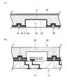
たとえば、特許文献1(特開2005-159258号公報)には、図18(A)に示すように、複数の基板101がマトリックス状に複数形成された基板集合体102を準備し、各基板101に電子部品素子(水晶振動素子)103を実装するとともに、複数の金属リッド104がマトリックス状に複数形成された金属リッド集合体105を準備し、続いて、図18(B)に示すように、接合材106を用いて、基板集合体102に金属リッド集合体105を接合して電子部品集合体107を形成し、最後に、図18(C)に示すように、電子部品集合体107を個々の電子部品(水晶振動子)108に分割する電子部品の製造方法が開示されている。
金属リッド104(金属リッド集合体105)は、たとえば、42アロイ、コバール、リン青銅などの金属板からなり、厚さは60μm~100μm程度で、板金加工により、電子部品素子103を収容するための凹部104aと、脚部104bとが形成されている。
基板101(基板集合体102)は、たとえば、ガラスセラミックス、アルミナセラミックスなどのセラミック材料からなり、一方の主面に、電子部品素子103を実装するためのランド電極101aと、金属リッド104を接合するための環状の接合電極101bとが形成されている。
接合材106は、たとえば、Au-Ni、Au-Snなどからなり、各基板101の接合電極101b上に設けられ、300℃~350℃に加熱され、溶融されて、接合電極101bと、金属リッド104の脚部104bとを接合している。
しかしながら、上述した従来の電子部品の製造方法には、金属リッド104(金属リッド集合体105)が、金属板に、板金加工をして、電子部品103を収容するための凹部104aと、基板101に接合するための脚部104bとを形成したものであるため、脚部104bの基板101aと当接する面の平坦性が低く、基板101aに接合した後の気密性が低いという問題があった。すなわち、平坦な金属板を用いても、プレス加工などで凹部104a、脚部104bを形成する際に、脚部104bの底面の平坦性が損なわれてしまい、接合後に気密漏れを生じてしまうおそれがあった。
このため、気密性を確保するためには、脚部104bの底面の幅を大きくしなければならず、電子部品が大型化してしまうという問題があった。
本発明は、上述した従来技術の問題点を解決するためになされたものである。その手段として、本発明の電子部品の製造方法は、基板を準備する工程と、基板に電子部品素子を実装する工程と、一方の主面に、周囲に環状の脚部を残して凹部が形成され、脚部の先端に接合材が供給された金属リッドを準備する工程と、金属リッドの凹部に前記電子部品素子を収容して、金属リッドを基板上に載置する工程と、熱エネルギーの印加により、接合材を用いて、金属リッドを基板に接合する工程とを備え、かつ、金属リッドの凹部は、平坦な金属板をエッチング加工することにより形成するようにした。
なお、本発明は、複数の基板がマトリックス状に形成された基板集合体と、複数の金属リッドがマトリックス状に形成された金属リッド集合体とを用いて、複数の電子部品を一括して大量に製造する場合にも適用することができる。すなわち、本発明の電子部品の製造方法の実施形態の1つは、複数の基板がマトリックス状に形成された基板集合体を準備する工程と、複数の基板のそれぞれに、電子部品素子を搭載する工程と、一方の主面に、周囲に環状の脚部を残して凹部が形成され、脚部の先端に接合材が供給された金属リッドが、複数、マトリックス状に形成された金属リッド集合体を準備する工程と、金属リッドの凹部のそれぞれに電子部品素子を収容して、金属リッド集合体を基板集合体上に実装する工程と、熱エネルギーの印加により、接合材を用いて、金属リッド集合体を基板集合体に接合し、電子部品集合体を形成する工程と、電子部品集合体を、個々の電子部品に分割する工程とを備え、かつ、複数の金属リッドの各凹部は、平坦な金属板をエッチング加工することにより形成するようにした。
本発明の電子部品の製造方法は、上記構成としたため、すなわち、金属リッドに平坦な金属板を用い、金属リッドの凹部を、板金加工ではなく、エッチング加工により形成するようにしたため、凹部の周囲に環状に形成される脚部の、基板と当接する端面の平坦性が、製造途中に損なわれることがない。したがって、本発明により製造された電子部品は、気密性に優れている。また、脚部の端面の幅を小さくしても、気密性が低下することがないため、脚部の端面の幅を小さくすることができ、電子部品を小型化することができる。
なお、接合材は、金属リッドの脚部の端面のみに供給することが好ましい。この場合には、基板と金属リッドを接合する際に、接合材が余剰となることがなく、余剰となった接合材が電子部品素子に付着するなどして電子部品の特性が劣化することがない。
また、金属リッドの脚部の端面に、接合材の収容部を形成するようにしても良い。この場合には、基板と金属リッドを接合する際に、余剰となった接合材をその収容部に収容することができ、余剰となった接合材が電子部品素子に付着するなどして電子部品の特性が劣化するのを防止することができる。
また、金属リッドの凹部の内壁に、不濡れ層を形成するようにしても良い。この場合には、基板と金属リッドを接合する際に、余剰となった接合材が金属リッドの凹部の内壁に濡れ拡がることがなく、そこから滴下して、電子部品素子に付着するなどして電子部品の特性が劣化することがない。また、接合材が金属リッドの凹部に濡れ拡がらないので、当初から接合材の供給量を少なくしておくことが可能であり、材料コストを低減することができる。
また、金属リッドの脚部の端面に、Niを主成分とする第1の層と、Auを主成分とする第2の層とからなるリッド電極を形成し、そのリッド電極上にBiを主成分とする接合材を供給するとともに、基板の、金属リッドと当接する部分に、Niを主成分とする第1の層と、Auを主成分とする第2の層とからなる接合電極を形成し、接合材でリッド電極と接合電極とを接合するようにしても良い。この場合には、Biを主成分とする接合材に、リッド電極および接合電極からAuとNiが拡散してBi‐Ni‐Au3元合金が形成されるが、Au、NiのBiへの拡散は速度が速いため、基板に金属リッドを短時間で接合することができる。また、Bi‐Ni‐Au3元合金は融点が高く、400℃以上であるため、製造された電子部品をリフローで実装する際に、再溶融することがなく、金属リッドが基板から外れてしまうことがない。
また、製造される電子部品は、平面方向に見た、基板の形状、大きさと、金属リッドの形状、大きさが、同一であることが好ましい。この場合には、金属リッドの天面の面積を最大にすることができ、その電子部品を真空吸着により保持して実装する際に、確実に吸着することができるからである。
以下、図面とともに、本発明を実施するための形態について説明する。
[第1実施形態]
図1(A)~図5(O)は、本発明の第1実施形態にかかる電子部品の製造方法において適用される、各工程を示す断面図である。
[第1実施形態]
図1(A)~図5(O)は、本発明の第1実施形態にかかる電子部品の製造方法において適用される、各工程を示す断面図である。
本実施形態にかかる電子部品の製造方法においては、複数の金属リッドがマトリックス状に形成された金属リッド集合体と、複数の基板がマトリックス状に形成された基板集合体とを準備し、両者を接合して電子部品集合体を形成した後に、電子部品集合体を個々の電子部品に分割する。以下、先に、金属リッド集合体について説明し、続いて、基板集合体について説明する。
図1(A)は、金属リッド集合体を製造するのに用いる金属板1を示す。金属板1には、主面の平坦性の高いものを用いる。たとえば金属板は圧延加工板を用いており、平面度は5μm以下であった。金属板1の材質は特に限定されないが、たとえば、コバール、42アロイなどのFe‐Ni系合金を用いることができる。金属板1の厚みは、製造する金属リッドの高さと同一にする。金属板1の大きさ(タテ、ヨコ)は、製造する金属リッドの大きさ、取り個数などを考慮して決定する。
次に、図1(B)に示すように、金属板1の両主面に、それぞれ、レジスト2aと2bとを形成する。レジスト2aは、金属板1の一方の主面(図中上側)の全面に形成する。レジスト2bは、金属板1の他方の主面(図中下側)に、複数の開口部(レジストを形成しない部分)2cを設けて部分的に形成する。開口部2cの形状、大きさ(タテ、ヨコ)は、製造する金属リッドに形成される凹部の形状、大きさと同一にする。開口部2cは、第1レジスト2bに、マトリクス状に形成する。
具体的には、たとえば、まず、金属板1の両主面に、ドライフィルムレジストを貼着する。次に、常用されているフォトリソグラフィープロセスにより、ドライフィルムレジストに、露光、現像などを施し、金属板1の一方の主面の全面にレジスト2a、他方の主面に複数の開口部2cが形成されたレジスト2bを得る。なお、金属板1の一方の主面に形成されたレジスト2aにも、たとえば、格子状の開口部を設け、後で分割する際のダイシング用の溝を、金属板1の表面に形成するようにしても良い。ドライフィルムレジストとしては、広く市販されているものを使用することができる。このドライフィルムレジストは、アルカリ水溶液、たとえばNaOHにより剥離することができる。
次に、図1(C)に示すように、たとえば、塩化第二鉄などのエッチング液を用いて、開口部2cから露出した金属板1をエッチングして、金属板1の他方の主面に、複数の凹部(製造する金属リッドの凹部)3を形成する。凹部3の深さは、収容する電子部品素子の高さに応じて、適宜、決定することができるが、本実施形態においては100μmとした。なお、凹部3は、上記のようにウエットプロセスで形成するのではなく、ドライプロセスで形成するようにしても良い。なお、本発明においては、凹部3がエッチング加工により形成されるため、製造途中において、金属板1の凹部3を形成した側の主面の平坦性が損なわれることがない。
次に、図2(D)に示すように、たとえば、NaOHなどのアルカリ水溶液を用いて、金属板1の両主面から、レジスト2a、2bを剥離する。
次に、図2(E)に示すように、金属板1の一方の主面に、めっきマスクシート5を貼着する。めっきマスクシート5には、広く市販されているものを使用することができる。
次に、図2(F)に示すように、金属板1に、一般的な電解めっき方法により、Niを主成分とする材料からなる、Ni層(リッド電極の第1層目)6を形成する。金属板1の一方の主面には、めっきマスクシート5が貼着されているため、Ni層6は形成されない。金属板1の他方の主面には、凹部3の内壁を含めて、Ni層6が形成される。なお、Ni層6の厚さは特に限定されないが、本実施形態においては1~5μmとした。
次に、図3(G)に示すように、Ni層(リッド電極の第1層目)6上に、一般的な電解めっき方法により、Auを主成分とする材料からなる、Au層(リッド電極の第2層目)7を形成する。金属板1の一方の主面には、めっきマスクシート5が貼着されているため、Au層7は形成されない。金属板1の他方の主面には、凹部3の内壁を含めて、Au層7が形成される。なお、Au層7の厚さは特に限定されないが、本実施形態においては0.1~1.0μmとした。
次に、図3(H)に示すように、Au層(リッド電極の第2層目)7上に、一般的な電解めっき方法により、Biを主成分とする材料からなる、Bi層(接合材層)8を形成する。金属板1の一方の主面には、めっきマスクシート5が貼着されているため、Bi層8は形成されない。金属板1の他方の主面には、凹部3の内壁を含めて、Bi層8が形成される。なお、Bi層8の厚さは特に限定されないが、本実施形態においては10μmとした。
なお、本実施形態では、上述のように、Ni層(リッド電極の第1層目)6、Au層(リッド電極の第2層目)7、Bi層(接合材層)8を、いずれも電解めっきで形成しているが、これに代えて、Ni層6、Au層7は蒸着やスパッタにより、Bi層8は蒸着やスパッタや印刷により形成するようにしても良い。また、接合材層であるBi層8に代えて、Sn‐Ag系はんだや、AuSnはんだを、接合材として用いても良い。
次に、図3(I)に示すように、金属板1の一方の主面から、めっきマスクシート5を剥離する。めっきマスクシート5の剥離は、たとえば、めっきマスクシート5の端部を冶具で把持し、引き剥がすことによりおこなう。
この結果、複数の金属リッド9がマトリックス状に複数形成された、金属リッド集合体10が完成する。(図3(I)においては、金属リッド9どうしの境界を鎖線で示す。)各金属リッド9は、他方の主面の中央に凹部9a(3)が形成され、凹部9aの周囲に環状の脚部9bが形成されている。そして、各脚部9bの端面(底面)には、Ni層(リッド電極の第1層目)6、Au層(リッド電極の第2層目)7、Bi層(接合材層)8が順に形成されている。
次に、基板集合体について説明する。
図4(J)は、複数の基板11がマトリックス状に複数形成された、基板集合体12を示す。(図4(J)においては、基板11どうしの境界を鎖線で示す。)基板11(基板集合体12)は、たとえば、多層セラミック基板からなり、一方の主面に、上述した金属リッド9(金属リッド集合体10)を接合するための、1層目がNi層13a、2層目がAu層14aからなる接合電極と、電子部品素子を実装するための、1層目がNi層13b、2層目がAu層14bからなるランド電極とが形成されている。なお、接合電極は、金属リッド9の脚部9bに対応して、環状に形成されている。そして、接合電極とランド電極はそれぞれ、基板11内部に形成されたビア導体と層間導体とからなる配線11aを経由して、基板11の他方の主面に形成された端子電極11bに接続されている。配線11a、端子電極11bの材質は特に限定されないが、たとえば、主成分にCu、Ag、Niなどを用いることができる。なお、完成した電子部品において、接合電極が接続された端子電極11bを接地すれば、接合電極に接合された金属リッド9を接地することができる。
基板11(基板集合体12)は、たとえば、次の方法で製造することができる。すなわち、まず、複数のセラミックのグリーンシートを用意し、所定のグリーンシートの表面に導電ペーストを塗布し、またビア内に導電ペーストを充填し、それらのグリーンシートを所定の順番に積層し、加圧し、所定のプロファイルで焼成して、配線11a、端子電極11b、接合電極の第1層目のNi層13a、ランド電極の第1層目のNi層13bの形成された基板11を得る。続いて、Ni層13a上に接合電極の第2層目のAu層14aを、Ni層13b上にランド電極の第2層目のAu層14bを、それぞれ、電解めっきなどの方法で形成することにより、基板11が完成する。本実施形態では、接合電極の第1層目のNi層13aおよびランド電極の1層目のNi層13bは、焼成により得たが、13aおよび13b上にめっきにてNi層を形成し、その上にAu層を形成しても良い。めっきによりNi層を形成することで、不純物の少ないNi層を得ることができる。
次に、図4(K)に示すように、各基板11のランド電極(Ni層13b、Au層14b)に、たとえば、導電性接着剤15を用いて、電子部品素子16を実装する。本実施形態においては、電子部品素子16として圧電素子を用いた。電子部品素子(圧電素子)16は、水晶などの圧電材料からなり、図示しないが、分極され、表面に複数の電極が形成されており、電極間に所定の電圧を印加すると、所定の周波数で振動し、たとえば発振子として機能する。なお、電子部品素子(圧電素子)16は、吸湿すると振動周波数が変動するおそれがあるため、パッケージ内に気密封止し、外部環境から保護する必要ものである。
次に、図4(L)に示すように、基板集合体12上に、金属リッド集合体10を載置する。このとき、各基板11上に、それぞれ金属リッド9が配置されるよう、位置合わせをおこなう。
次に、図5(M)に示すように、基板集合体12、および基板集合体12上に載置された金属リッド集合体10を、上下方向からボンディングツール17a、17bで挟み込み、たとえば、1~10分間、5~20MPaの圧力で加圧し、250~350℃で加熱して、Bi層(接合材層)8を溶融させ、金属リッド9の脚部9bの端面に形成されたNi層(リッド電極の第1層目)6、Au層(リッド電極の第2層目)7と、基板11に形成されたNi層13a(接合電極の第1層目)、Au層14a(接合電極の第2層目)とから、Bi層(接合材層)8にAuとNiを拡散させる。この結果、図5(N)に示すように、Bi‐Ni‐Au3元合金層18が形成され、金属リッド集合体10が基板集合体12に接合され、複数の電子部品19がマトリックス状に配置された電子部品集合体20が形成される。
Bi‐Ni‐Au3元合金層18は、融点が400℃以上であるため、本実施形態の製造方法により製造された電子部品を、リフローはんだなどで実装する際に加熱されても、再溶融することがなく、信頼性の高い接合を得ることができる。なお、上述のとおり、接合材層であるBi層8に代えて、Sn‐Ag系はんだや、AuSnはんだを接合材として用いることができるが、この場合も同様の加圧、加熱プロセスで接合することができる。ただし、Biを接合材に用いた方が、低コストで、より再溶融しにくい接合を得ることができる。
最後に、複数の電子部品19がマトリックス状に配置された電子部品集合体20を、図5(N)に鎖線で示す、X‐X部分、Y‐Y部分、Z‐Z部分などで、ダイシングなどの工法により分割して、個々の電子部品(圧電振動子)19を得る。電子部品19は、Bi‐Ni‐Au3元合金層18により、金属リッド9が基板11に堅固に接合されている。なお、Bi‐Ni‐Au3元合金層18と接続された接続端子11bを接地すれば、金属リッド9により、金属リッド9の凹部9bの内部を良好にシールドすることができる。
なお、完成した電子部品19は、平面方向に見て、基板11の形状、大きさと、金属リッド19の形状、大きさが、同一になっている。したがって、電子部品19は、金属リッド19の天面の面積が最大になっており、真空吸着により保持して実装する際に、確実に吸着することができる。
以上、本発明の第1実施形態にかかる、電子部品の製造方法について説明した。しかしながら、本発明が上記の内容に限定されることはなく、発明の主旨に沿って、種々の変更をなすことができる。
たとえば、本実施形態においては、リッド電極9の脚部9aの端面に、リッド電極として、Ni層6、Au層7、接合材層としてBi層8を形成し、基板11の一方の主面上に、接合電極としてNi層13a、Au層14aを形成しているが、これらの種類、層数、厚みなどは任意であり、たとえば、他の材料を用いたり、層数を増減させたりすることができる。
また、本実施形態においては、電子部品として圧電振動子を製造したが、製造される電子部品は圧電振動子には限られず、他の電子部品、たとえば、ジャイロや、弾性表面波装置などであっても良い。
[第2実施形態]
図6(A)~(C)は、本発明の第2実施形態にかかる電子部品の製造方法において適用される、各工程を示す工程図である。
図6(A)~(C)は、本発明の第2実施形態にかかる電子部品の製造方法において適用される、各工程を示す工程図である。
第2実施形態にかかる電子部品の製造方法は、図1(A)~図5(O)に示した、第1実施形態にかかる電子部品の製造方法の工程の一部を変更したものである。
すなわち、第2実施形態にかかる電子部品の製造方法は、図1(C)に示した、金属板1の他方の主面に、たとえば、エッチングにより複数の凹部3を形成するところまでは、第1実施形態と同じ工程を用いる。
第2実施形態では、次に、図6(A)に示すように、金属板1から、他方の主面(図中下側)に形成されたレジスト2bのみを剥離する。すなわち、金属基板1の一方の主面(図中上側)に形成されたレジスト2aは剥離しない。この工程は、たとえば、金属基板1の他方の主面のみをアルカリ水溶液に浸漬する、あるいは、金属基板1の一方の主面に形成されたレジスト2aをマスクしたうえで、金属基板1をアルカリ水溶液に浸漬するなどの方法によりおこなうことができる。
次に、図6(B)に示すように、金属板1の他方の主面に、Ni層(リッド電極の第1層目)6、Au層(リッド電極の第2層目)7、Bi層(接合材層)8を、順に、電解めっきで形成する。金属板1の一方の主面には、レジスト2aが形成されているため、Ni層6、Au層7、Bi層8は形成されない。
次に、図6(C)に示すように、金属板1の一方の主面からアルカリ水溶液を用いてレジスト2aを剥離することにより、中央に凹部9a(3)が形成され、凹部9aの周囲に環状の脚部9bが形成され金属リッド9が、マトリックス状に複数形成された金属リッド集合体10が完成する。
この後、第2実施形態においても、第1実施形態と同様に、図4(J)以降の工程を施す。
以上のように、第2実施形態においては、金属板1の他方の主面に、Ni層6、Au層7、Bi層8を形成する際に、金属板1の一方の主面をレジスト2aで覆い、これらが形成されないようにした。したがって、本実施形態においては、第1実施形態において使用した、めっきマスクシート5の使用を省略することができる。
[第3実施形態]
図7(A)~図8(E)は、本発明の第3実施形態にかかる電子部品の製造方法において適用される、各工程を示す工程図である。
図7(A)~図8(E)は、本発明の第3実施形態にかかる電子部品の製造方法において適用される、各工程を示す工程図である。
第3実施形態にかかる電子部品の製造方法は、図1(A)~図5(O)に示した、第1実施形態にかかる電子部品の製造方法の工程の一部を変更したものである。
すなわち、第3実施形態にかかる電子部品の製造方法は、図1(C)に示した、金属板1の他方の主面に、たとえば、エッチングにより複数の凹部3を形成するところまでは、第1実施形態と同じ工程を用いる。
第3実施形態においては、次に、図7(A)に示すように、凹部3の内壁に、第2のレジスト22を形成する。本実施形態においては、第2のレジスト22を電着レジストにより形成する。
具体的には、まず、金属板1全体を、酸系表面処理液に浸漬し、凹部3の内壁の脱脂、洗浄をおこなう。次に、金属板1全体を、液温40℃の、株式会社シミズ製、商品名「エレコートEU-XC」に浸漬し、金属板1を陰極として、SUS板を陽極として、DC100Vの電流を30秒間通電し、凹部3の内壁に、厚さ10μm程度の電着レジスト膜を形成する。次に、乾燥、露光、現像をして、凹部3の内壁に、第2のレジスト22を得る。第2のレジスト22は、酸水溶液により剥離するが、アルカリ水溶液では剥離しない。
次に、図7(B)に示すように、たとえば、NaOHなどのアルカリ水溶液を用いて、金属基板1の両主面から、レジスト2a、2bを剥離する。このとき、第2のレジスト22は、上述のとおり、アルカリ水溶液では剥離しないので、残存する。
次に、図7(C)に示すように、金属板1の一方の主面に、めっきマスクシート5を貼着する。めっきマスクシート5には、広く市販されているものを使用することができる。
次に、図8(D)に示すように、金属板1に、Ni層(リッド電極の第1層目)26、Au層(リッド電極の第2層目)27、Bi層(接合材層)28を、順に、電解めっきで形成する。金属板1の一方の主面には、めっきマスクシート5が形成されているため、Ni層26、Au層27、Bi層28は形成されない。また、金属板1の他方の主面に形成された凹部3の内壁にも、第2のレジスト22が形成されているため、Ni層26、Au層27、Bi層28は形成されない。
次に、図8(E)に示すように、金属板1の一方の主面からめっきマスクシート5を剥離するとともに、凹部3の内壁から第2のレジスト22を剥離する。めっきマスクシート5の剥離と、第2のレジスト4の剥離とは、どちらを先におこなっても良い。めっきマスクシート5の剥離は、たとえば、めっきマスクシート5の端部を冶具で把持し、引き剥がすことによりおこなう。第2のレジスト22の剥離は、酸水溶液、たとえば、シミズ製「DLP‐42」を用いておこなう。なお、第2のレジスト22の剥離は必須ではなく、凹部3内に残存させておいても良い。この結果、中央に凹部9a(3)が形成され、凹部9aの周囲に環状の脚部9bが形成され金属リッド9が、マトリックス状に複数形成された金属リッド集合体10が完成する。
この後、第3実施形態においても、第1実施形態と同様に、図4(J)以降の工程を施す。
以上のように、第3実施形態においては、金属リッド9の脚部9bの端面のみに、Ni層26、Au層27、Bi層28を形成し、金属リッド9の凹部9(3)の内壁には、これらを形成しないようにした。このような構造にした場合には、基板11と金属リッド9とを接合する際に、接合材であるBi層28のBiが余剰となることがなく、余剰となった接合材が電子部品素子16に付着するなどして電子部品の特性が劣化することがない。
[第4実施形態]
図9(A)は、本発明の第4実施形態にかかる電子部品の製造方法において適用される工程を示す工程図である。
図9(A)は、本発明の第4実施形態にかかる電子部品の製造方法において適用される工程を示す工程図である。
第4実施形態にかかる電子部品の製造方法は、図7(A)~図8(E)に示した、第3実施形態にかかる電子部品の製造方法の工程の一部を変更したものである。
すなわち、第4実施形態にかかる電子部品の製造方法は、図8(E)に示した、金属板1の一方の主面からめっきマスクシート5を、凹部9a(3)の内壁から第2のレジスト22を剥離するところまでは、第3実施形態と同じ工程を用いる。
第4の実施形態においては、次に、図9(A)に示すように、第2のレジスト22を剥離した凹部9a(3)の内壁に、改めて、不濡れ層23を形成する。不濡れ層23は、たとえば、酸素プラズマによるドライプロセスにより、金属板1の凹部9a(3)の内壁に露出した部分を酸化させることにより形成する。あるいは、濡れ性の悪い無機膜や有機膜を、別途、形成しても良い。あるいは、第3実施形態で、金属板1の凹部9a(3)の内壁に形成した第2のレジスト22を、剥離せず、残存させて、不濡れ層23としても良い。
第4実施形態においても、この後、第3実施形態と同様の工程を施す。
以上のように、第4実施形態においては、金属リッド9の凹部9a(3)の内壁に不濡れ層23が形成される。このような構造にした場合には、基板11と金属リッド9とを接合する際に、接合材であるBi層28のBiが余剰となったとしても、金属リッド9の凹部9a(3)の内壁に濡れ拡がることがなく、そこから滴下して、電子部品素子16に付着するなどして電子部品の特性が劣化することがない。
[第5実施形態]
図10(A)~図15(M)は、本発明の第5実施形態にかかる電子部品の製造方法において適用される、各工程を示す断面図である。
図10(A)~図15(M)は、本発明の第5実施形態にかかる電子部品の製造方法において適用される、各工程を示す断面図である。
まず、図10(A)に示すように、金属リッド集合体を製造するのに用いる金属板31を準備する。
次に、図10(B)に示すように、金属板31の両主面に、それぞれ、レジスト32aと32bとを形成する。レジスト32aは、金属板31の一方の主面(図中上側)の全面に形成する。レジスト32bは、金属板31の他方の主面(図中下側)に、複数の開口部32cを設けて部分的に形成する。
次に、図10(C)に示すように、エッチング液を用いて、開口部32cから露出した金属板31をエッチングして、金属板31の他方の主面に、複数の、余剰となった接合材を収容するための収容部33を形成する。
次に、図11(D)に示すように、アルカリ水溶液を用いて、金属板31の両主面から、レジスト32a、32bを剥離する。
次に、図11(E)に示すように、金属板31の両主面に、それぞれ、改めて、レジスト42aと42bとを形成する。レジスト42aは、金属板31の一方の主面(図中上側)の全面に形成する。レジスト42bは、金属板31の他方の主面(図中下側)に、複数の開口部42cを設けて部分的に形成する。なお、レジスト42bは、先に金属板31に形成した、収容部33を塞ぐように形成する。
次に、図11(F)に示すように、エッチング液を用いて、開口部42cから露出した金属板31をエッチングして、金属板31の他方の主面に、電子部品素子を収容するための凹部43を形成する。
次に、図12(G)に示すように、凹部43の内壁に、電着レジストにより、第2のレジスト52を形成する。
次に、図12(H)に示すように、アルカリ水溶液を用いて、金属板31の両主面から、レジスト42a、42bを剥離する。
次に、図12(I)に示すように、金属板31の一方の主面に、めっきマスクシート35を貼着する。
次に、図13(J)に示すように、金属板31に、Ni層(リッド電極の第1層目)36、Au層(リッド電極の第2層目)37、Bi層(接合材層)38を、順に、電解めっきで形成する。Ni層36、Au層37、Bi層38は、第2のレジスト52が形成されているため凹部43の内壁には形成されないが、収容部43の内壁には形成される。
次に、図13(K)に示すように、金属板31の一方の主面から、めっきマスクシート35を剥離するとともに、凹部43の内壁から第2のレジスト52を剥離し、複数の金属リッド39がマトリックス状に形成された金属リッド集合体40を完成させて、これを、複数の基板11がマトリックス状に形成された基板集合体12上に載置する。
次に、図14(L)に示すように、基板集合体12、および基板集合体12上に載置された金属リッド集合体40を、上下方向からボンディングツール17a、17bで挟み込み、加圧し、加熱して、Bi層38を溶融させ、金属リッド39の脚部39bの端面に形成されたNi層36、Au層37と、基板11に形成されたNi層13a、Au層14aとから、Bi層38にAuとNiを拡散させる。
この結果、図14(M)に示すように、Bi‐Ni‐Au3元合金層48が形成され、金属リッド集合体10が基板集合体12に接合され、複数の電子部品49がマトリックス状に配置された電子部品集合体50が形成される。
このとき、余剰となったBi‐Ni‐Au3元合金層48は、金属リッド39に形成した収容部33に収容されるため、金属リッド39の凹部39a(43)側に流れてゆくことがなく、電子部品素子16に付着することがない。
最後に、複数の電子部品49がマトリックス状に配置された電子部品集合体50を、図14(M)に鎖線で示す、S‐S部分、T‐T部分などで分割して、図15(N)に示すように、個々の電子部品49を得る。
第5実施形態においては、金属リッド39の脚部39bに収容部33を形成し、基板11と金属リッド39を接合する際に、余剰となった接合材であるBi層38のBiを、収容部33に収容するようにしているため、Biが電子部品素子16に付着するなどして電子部品の特性が劣化することがない。
[第6実施形態]
図16(A)~図17(D)は、本発明の第6実施形態にかかる電子部品の製造方法において適用される、各工程を示す工程図である。
図16(A)~図17(D)は、本発明の第6実施形態にかかる電子部品の製造方法において適用される、各工程を示す工程図である。
第6実施形態にかかる電子部品の製造方法は、図1(A)~図5(O)に示した、第1実施形態にかかる電子部品の製造方法の工程の一部を変更したものである。
すなわち、第6実施形態にかかる電子部品の製造方法は、図3(I)に示した、複数の金属リッド9がマトリック状に形成された金属リッド集合体10を製造するところまで、また、図4(K)に示した、複数の基板11がマトリック状に形成された基板集合体12を製造し、各基板11に電子部品素子16を実装するところまでは、第1実施形態と同じ工程を用いる。
第6実施形態においては、次に、図16(A)に示すように、金属リッド集合体10を個々の金属リッド9に分割し、金属製の冶具51aに貼着する。貼着は、図示しないが、たとえば、金属製の冶具51a表面に設置された、タック性を有するゴムシートを介しておこなう。
次に、図16(B)に示すように、電子部品素子16を実装した基板集合体12を個々の基板11に分割し、同様に、金属製の冶具51bに貼着する。
次に、図16(C)に示すように、冶具51bに貼着された基板11上に、冶具51aに貼着された金属リッド9を載置する。冶具51bには複数の基板11が貼着され、冶具51aには複数の金属リッド9が貼着されており、この工程は多数個を一括しておこなう。
最後に、図17(D)に示すように、冶具51a、51bを、上下方向からボンディングツール17a、17bで挟み込み、加圧し、加熱して、基板11に金属リッド9を接合して、電子部品19を完成させる。
このように、本発明の電子部品の製造方法は、金属リッド集合体10と基板集合体12とを接合した後に、個々の電子部品19に分割するのではなく、金属リッド集合体10を個々の金属リッド9に分割し、基板集合体12を個々の基板11に分割し、それらの金属リッド9と基板11を接合するという形態においても実施することができる。これにより、分割工程時の負荷による電子部品素子16の破壊を防ぐことができる。あるいは、寸法精度の悪い集合基板に対して、本工法を適用することが可能になる。
1、31:金属板
2a、2b、32a、32b、42a、42b:レジスト
2c、32c、42c:開口部(レジストを形成しない部分)
3、43:凹部
5、35:めっきマスクシート
6、26、36:Ni層(リッド電極の第1層目)
7、27、37:Au層(リッド電極の第2層目)
8、28、38:Bi層(接合材層)
9、39:金属リッド
10、40:金属リッド集合体
11:基板
11a:配線
11b:端子電極
12:基板集合体
13a:Ni層(接合電極の第1層目)
13b:Ni層(ランド電極の第1層目)
14a:Au層(接合電極の第2層目)
14b:Au層(ランド電極の第2層目)
15:導電性接着剤
16:圧電素子(電子部品素子)
17a、17b:ボンディングツール
18:Bi‐Ni‐Au3元合金層
19、49:圧電振動子(電子部品)
20、50:電子部品集合体
22:第2のレジスト
23:不濡れ層
33:収容部
51a、51b:冶具
Claims (8)
- 基板を準備する工程と、
前記基板に電子部品素子を実装する工程と、
一方の主面に、周囲に環状の脚部を残して凹部が形成され、前記脚部の先端に接合材が供給された金属リッドを準備する工程と、
前記金属リッドの凹部に前記電子部品素子を収容して、前記金属リッドを前記基板上に載置する工程と、
熱エネルギーの印加により、前記接合材を用いて、前記金属リッドを前記基板に接合する工程とを備えた電子部品の製造方法であって、
前記金属リッドの凹部は、平坦な金属板をエッチング加工することにより形成される電子部品の製造方法。 - 複数の基板がマトリックス状に形成された基板集合体を準備する工程と、
前記複数の基板のそれぞれに、電子部品素子を実装する工程と、
一方の主面に、周囲に環状の脚部を残して凹部が形成され、前記脚部の先端に接合材が供給された金属リッドが、複数、マトリックス状に形成された金属リッド集合体を準備する工程と、
前記金属リッドの凹部のそれぞれに前記電子部品素子を収容して、前記金属リッド集合体を前記基板集合体上に載置する工程と、
熱エネルギーの印加により、前記接合材を用いて、前記金属リッド集合体を前記基板集合体に接合し、電子部品集合体を形成する工程と、
前記電子部品集合体を、個々の電子部品に分割する工程とを備えた電子部品の製造方法であって、
前記複数の金属リッドの凹部は、平坦な金属板をエッチング加工することにより形成される電子部品の製造方法。 - 前記金属リッドの前記脚部の端面のみに、前記接合材が供給された、請求項1または2に記載された電子部品の製造方法。
- 前記金属リッドの前記脚部の端面に、余剰となった前記接合材を収容するための収容部が形成された、請求項1ないし3のいずれか1項に記載された電子部品の製造方法。
- 前記金属リッドの前記凹部の内壁に、不濡れ層が形成された、請求項1ないし4のいずれか1項に記載された電子部品の製造方法。
- 前記金属リッドの前記脚部の端面にリッド電極が形成され、当該リッド電極上に前記接合材が供給され、
前記基板の、前記金属リッドと当接する部分に接合電極が形成され、
前記リッド電極および前記接合電極はいずれも、Niを主成分とする第1の層と、Auを主成分とする第2の層とからなり、
前記接合材がBiを主成分とする、請求項1ないし5のいずれか1項に記載された電子部品の製造方法。 - 基板と、
前記基板に実装された電子部品素子と、
一方の主面に、周囲に環状の脚部を残して凹部が形成され、当該凹部に前記電子部品素子を収容して、前記基板に接合された金属リッドとを備えた電子部品であって、
前記金属リッドの前記凹部の内壁に、不濡れ層が形成されている電子部品。 - 基板と、
前記基板に実装された電子部品素子と、
一方の主面に、周囲に環状の脚部を残して凹部が形成され、当該凹部に前記電子部品素子を収容して、前記基板に接合された金属リッドとを備えた電子部品であって、
平面方向に見て、前記基板の形状、大きさと、前記金属リッドの形状、大きさが同一である電子部品。
Priority Applications (1)
| Application Number | Priority Date | Filing Date | Title |
|---|---|---|---|
| JP2012527688A JPWO2012017888A1 (ja) | 2010-08-04 | 2011-07-27 | 電子部品の製造方法および電子部品 |
Applications Claiming Priority (2)
| Application Number | Priority Date | Filing Date | Title |
|---|---|---|---|
| JP2010175423 | 2010-08-04 | ||
| JP2010-175423 | 2010-08-04 |
Publications (1)
| Publication Number | Publication Date |
|---|---|
| WO2012017888A1 true WO2012017888A1 (ja) | 2012-02-09 |
Family
ID=45559389
Family Applications (1)
| Application Number | Title | Priority Date | Filing Date |
|---|---|---|---|
| PCT/JP2011/067071 WO2012017888A1 (ja) | 2010-08-04 | 2011-07-27 | 電子部品の製造方法および電子部品 |
Country Status (2)
| Country | Link |
|---|---|
| JP (1) | JPWO2012017888A1 (ja) |
| WO (1) | WO2012017888A1 (ja) |
Cited By (1)
| Publication number | Priority date | Publication date | Assignee | Title |
|---|---|---|---|---|
| JP2014165305A (ja) * | 2013-02-25 | 2014-09-08 | Kyocera Crystal Device Corp | 電子デバイス及びそのガラス封止方法並びに電子デバイス用蓋部材 |
Citations (6)
| Publication number | Priority date | Publication date | Assignee | Title |
|---|---|---|---|---|
| JP2002064159A (ja) * | 2000-08-21 | 2002-02-28 | Murata Mfg Co Ltd | 電子部品用金属キャップ、その製造方法及び電子部品 |
| JP2006295246A (ja) * | 2005-04-05 | 2006-10-26 | Matsushita Electric Ind Co Ltd | 電子部品とその製造方法 |
| JP2007096777A (ja) * | 2005-09-29 | 2007-04-12 | Kyocera Kinseki Corp | 圧電振動子の製造方法 |
| WO2010021268A1 (ja) * | 2008-08-21 | 2010-02-25 | 株式会社村田製作所 | 電子部品装置およびその製造方法 |
| JP2010060541A (ja) * | 2008-09-08 | 2010-03-18 | Torex Semiconductor Ltd | 半導体センサー装置 |
| JP2011139223A (ja) * | 2009-12-28 | 2011-07-14 | Kyocera Kinseki Corp | 蓋部材及び蓋部材ウエハの製造方法及び蓋部材の製造方法 |
Family Cites Families (5)
| Publication number | Priority date | Publication date | Assignee | Title |
|---|---|---|---|---|
| JPH0496256A (ja) * | 1990-08-03 | 1992-03-27 | Mitsubishi Materials Corp | 金属製ハーメチックシール蓋 |
| JP3432988B2 (ja) * | 1996-01-18 | 2003-08-04 | 日本特殊陶業株式会社 | 電子部品パッケージ用金属製リッド基板、及び金属製リッドの製造方法 |
| JP3663343B2 (ja) * | 2000-07-14 | 2005-06-22 | 京セラ株式会社 | 半導体素子収納用パッケージ |
| JP3783605B2 (ja) * | 2001-10-29 | 2006-06-07 | 松下電器産業株式会社 | 気密封止パッケージおよびこれを用いたデバイス |
| JP5538974B2 (ja) * | 2010-03-26 | 2014-07-02 | セイコーインスツル株式会社 | 電子デバイスパッケージの製造方法及び電子デバイスパッケージ |
-
2011
- 2011-07-27 JP JP2012527688A patent/JPWO2012017888A1/ja active Pending
- 2011-07-27 WO PCT/JP2011/067071 patent/WO2012017888A1/ja active Application Filing
Patent Citations (6)
| Publication number | Priority date | Publication date | Assignee | Title |
|---|---|---|---|---|
| JP2002064159A (ja) * | 2000-08-21 | 2002-02-28 | Murata Mfg Co Ltd | 電子部品用金属キャップ、その製造方法及び電子部品 |
| JP2006295246A (ja) * | 2005-04-05 | 2006-10-26 | Matsushita Electric Ind Co Ltd | 電子部品とその製造方法 |
| JP2007096777A (ja) * | 2005-09-29 | 2007-04-12 | Kyocera Kinseki Corp | 圧電振動子の製造方法 |
| WO2010021268A1 (ja) * | 2008-08-21 | 2010-02-25 | 株式会社村田製作所 | 電子部品装置およびその製造方法 |
| JP2010060541A (ja) * | 2008-09-08 | 2010-03-18 | Torex Semiconductor Ltd | 半導体センサー装置 |
| JP2011139223A (ja) * | 2009-12-28 | 2011-07-14 | Kyocera Kinseki Corp | 蓋部材及び蓋部材ウエハの製造方法及び蓋部材の製造方法 |
Cited By (1)
| Publication number | Priority date | Publication date | Assignee | Title |
|---|---|---|---|---|
| JP2014165305A (ja) * | 2013-02-25 | 2014-09-08 | Kyocera Crystal Device Corp | 電子デバイス及びそのガラス封止方法並びに電子デバイス用蓋部材 |
Also Published As
| Publication number | Publication date |
|---|---|
| JPWO2012017888A1 (ja) | 2013-10-03 |
Similar Documents
| Publication | Publication Date | Title |
|---|---|---|
| TWI517310B (zh) | Manufacturing method of electronic device package | |
| JP5538974B2 (ja) | 電子デバイスパッケージの製造方法及び電子デバイスパッケージ | |
| TW201521359A (zh) | 表面安裝晶體振子 | |
| JP2011147054A (ja) | 電子装置、および、電子装置の製造方法 | |
| TW201531437A (zh) | 電子裝置及電子裝置的製造方法 | |
| TWI640161B (zh) | 電子裝置及電子裝置的製造方法 | |
| WO2012017888A1 (ja) | 電子部品の製造方法および電子部品 | |
| JP2005129600A (ja) | 金属パッケージ及びその製造方法、並びに電子デバイス | |
| JP2005072050A (ja) | 電子デバイス基板、電子デバイス及びその製造方法 | |
| JP2012028454A (ja) | 部分めっき方法、金属製蓋部材、および電子部品。 | |
| JPH11126847A (ja) | 電子部品収納用パッケージ | |
| JP5253437B2 (ja) | 表面実装用の水晶振動子 | |
| JP6482282B2 (ja) | 電子部品 | |
| JP2007184810A (ja) | 圧電振動子の製造方法 | |
| JP2005079656A (ja) | 圧電振動子 | |
| JP2012028453A (ja) | 金属製ハーメチック蓋の製造方法 | |
| JP2010057095A (ja) | 圧電振動子及びその製造方法並びに発振器 | |
| JP2001308211A (ja) | 電子部品収納用パッケージ | |
| JP5220539B2 (ja) | 圧電振動子の製造方法 | |
| JP2018190933A (ja) | 配線基板及びその製造方法 | |
| JP2004363936A (ja) | 表面実装型水晶振動子とその製造方法 | |
| JPH09116047A (ja) | セラミックパッケージの構造 | |
| JP2010087926A (ja) | 電子部品用容器体および電子部品用容器体の製造方法 | |
| JP2006339791A (ja) | 圧電デバイスの製造方法 | |
| JP5278950B2 (ja) | 圧電振動子のパッケージの製造方法 |
Legal Events
| Date | Code | Title | Description |
|---|---|---|---|
| 121 | Ep: the epo has been informed by wipo that ep was designated in this application |
Ref document number: 11814515 Country of ref document: EP Kind code of ref document: A1 |
|
| WWE | Wipo information: entry into national phase |
Ref document number: 2012527688 Country of ref document: JP |
|
| NENP | Non-entry into the national phase |
Ref country code: DE |
|
| 122 | Ep: pct application non-entry in european phase |
Ref document number: 11814515 Country of ref document: EP Kind code of ref document: A1 |