WO2012017838A1 - 光源装置 - Google Patents
光源装置 Download PDFInfo
- Publication number
- WO2012017838A1 WO2012017838A1 PCT/JP2011/066671 JP2011066671W WO2012017838A1 WO 2012017838 A1 WO2012017838 A1 WO 2012017838A1 JP 2011066671 W JP2011066671 W JP 2011066671W WO 2012017838 A1 WO2012017838 A1 WO 2012017838A1
- Authority
- WO
- WIPO (PCT)
- Prior art keywords
- excitation light
- light
- wavelength conversion
- light source
- wavelength
- Prior art date
Links
- 230000005284 excitation Effects 0.000 claims abstract description 219
- 238000006243 chemical reaction Methods 0.000 claims abstract description 158
- 230000005540 biological transmission Effects 0.000 claims abstract description 20
- 230000003287 optical effect Effects 0.000 claims abstract description 14
- 238000000034 method Methods 0.000 claims description 16
- 238000007740 vapor deposition Methods 0.000 claims description 7
- 238000003980 solgel method Methods 0.000 claims description 4
- 239000010410 layer Substances 0.000 description 83
- OAICVXFJPJFONN-UHFFFAOYSA-N Phosphorus Chemical compound [P] OAICVXFJPJFONN-UHFFFAOYSA-N 0.000 description 15
- 239000011521 glass Substances 0.000 description 8
- 239000007787 solid Substances 0.000 description 7
- 230000000052 comparative effect Effects 0.000 description 6
- 239000000463 material Substances 0.000 description 6
- 229910004298 SiO 2 Inorganic materials 0.000 description 5
- 229910010413 TiO 2 Inorganic materials 0.000 description 4
- 108010025899 gelatin film Proteins 0.000 description 4
- 238000010586 diagram Methods 0.000 description 3
- 230000000694 effects Effects 0.000 description 3
- 229910052751 metal Inorganic materials 0.000 description 3
- 239000002184 metal Substances 0.000 description 3
- 238000012986 modification Methods 0.000 description 3
- 230000004048 modification Effects 0.000 description 3
- 229920005989 resin Polymers 0.000 description 3
- 239000011347 resin Substances 0.000 description 3
- VYPSYNLAJGMNEJ-UHFFFAOYSA-N Silicium dioxide Chemical compound O=[Si]=O VYPSYNLAJGMNEJ-UHFFFAOYSA-N 0.000 description 2
- 238000010521 absorption reaction Methods 0.000 description 2
- 150000004703 alkoxides Chemical class 0.000 description 2
- 239000011230 binding agent Substances 0.000 description 2
- 238000000151 deposition Methods 0.000 description 2
- 238000010304 firing Methods 0.000 description 2
- 230000007062 hydrolysis Effects 0.000 description 2
- 238000006460 hydrolysis reaction Methods 0.000 description 2
- 239000007788 liquid Substances 0.000 description 2
- 239000002245 particle Substances 0.000 description 2
- 238000006068 polycondensation reaction Methods 0.000 description 2
- 239000011241 protective layer Substances 0.000 description 2
- 238000005086 pumping Methods 0.000 description 2
- XUIMIQQOPSSXEZ-UHFFFAOYSA-N Silicon Chemical compound [Si] XUIMIQQOPSSXEZ-UHFFFAOYSA-N 0.000 description 1
- 230000007423 decrease Effects 0.000 description 1
- 230000006866 deterioration Effects 0.000 description 1
- 238000005259 measurement Methods 0.000 description 1
- 239000000203 mixture Substances 0.000 description 1
- 238000005498 polishing Methods 0.000 description 1
- 230000005855 radiation Effects 0.000 description 1
- 229910052710 silicon Inorganic materials 0.000 description 1
- 239000010703 silicon Substances 0.000 description 1
- 229920002050 silicone resin Polymers 0.000 description 1
- 229910052709 silver Inorganic materials 0.000 description 1
- 239000004332 silver Substances 0.000 description 1
- 239000000126 substance Substances 0.000 description 1
- XLYOFNOQVPJJNP-UHFFFAOYSA-N water Substances O XLYOFNOQVPJJNP-UHFFFAOYSA-N 0.000 description 1
Images

Classifications
-
- C—CHEMISTRY; METALLURGY
- C09—DYES; PAINTS; POLISHES; NATURAL RESINS; ADHESIVES; COMPOSITIONS NOT OTHERWISE PROVIDED FOR; APPLICATIONS OF MATERIALS NOT OTHERWISE PROVIDED FOR
- C09K—MATERIALS FOR MISCELLANEOUS APPLICATIONS, NOT PROVIDED FOR ELSEWHERE
- C09K11/00—Luminescent, e.g. electroluminescent, chemiluminescent materials
- C09K11/08—Luminescent, e.g. electroluminescent, chemiluminescent materials containing inorganic luminescent materials
- C09K11/64—Luminescent, e.g. electroluminescent, chemiluminescent materials containing inorganic luminescent materials containing aluminium
- C09K11/646—Silicates
-
- G—PHYSICS
- G02—OPTICS
- G02B—OPTICAL ELEMENTS, SYSTEMS OR APPARATUS
- G02B19/00—Condensers, e.g. light collectors or similar non-imaging optics
- G02B19/0004—Condensers, e.g. light collectors or similar non-imaging optics characterised by the optical means employed
- G02B19/0009—Condensers, e.g. light collectors or similar non-imaging optics characterised by the optical means employed having refractive surfaces only
- G02B19/0014—Condensers, e.g. light collectors or similar non-imaging optics characterised by the optical means employed having refractive surfaces only at least one surface having optical power
-
- G—PHYSICS
- G02—OPTICS
- G02B—OPTICAL ELEMENTS, SYSTEMS OR APPARATUS
- G02B19/00—Condensers, e.g. light collectors or similar non-imaging optics
- G02B19/0033—Condensers, e.g. light collectors or similar non-imaging optics characterised by the use
- G02B19/0047—Condensers, e.g. light collectors or similar non-imaging optics characterised by the use for use with a light source
-
- G—PHYSICS
- G02—OPTICS
- G02B—OPTICAL ELEMENTS, SYSTEMS OR APPARATUS
- G02B27/00—Optical systems or apparatus not provided for by any of the groups G02B1/00 - G02B26/00, G02B30/00
- G02B27/10—Beam splitting or combining systems
- G02B27/106—Beam splitting or combining systems for splitting or combining a plurality of identical beams or images, e.g. image replication
-
- G—PHYSICS
- G02—OPTICS
- G02B—OPTICAL ELEMENTS, SYSTEMS OR APPARATUS
- G02B27/00—Optical systems or apparatus not provided for by any of the groups G02B1/00 - G02B26/00, G02B30/00
- G02B27/10—Beam splitting or combining systems
- G02B27/14—Beam splitting or combining systems operating by reflection only
- G02B27/142—Coating structures, e.g. thin films multilayers
-
- G—PHYSICS
- G02—OPTICS
- G02B—OPTICAL ELEMENTS, SYSTEMS OR APPARATUS
- G02B5/00—Optical elements other than lenses
- G02B5/02—Diffusing elements; Afocal elements
- G02B5/0205—Diffusing elements; Afocal elements characterised by the diffusing properties
- G02B5/0236—Diffusing elements; Afocal elements characterised by the diffusing properties the diffusion taking place within the volume of the element
-
- G—PHYSICS
- G02—OPTICS
- G02B—OPTICAL ELEMENTS, SYSTEMS OR APPARATUS
- G02B5/00—Optical elements other than lenses
- G02B5/02—Diffusing elements; Afocal elements
- G02B5/0273—Diffusing elements; Afocal elements characterized by the use
- G02B5/0278—Diffusing elements; Afocal elements characterized by the use used in transmission
-
- G—PHYSICS
- G02—OPTICS
- G02B—OPTICAL ELEMENTS, SYSTEMS OR APPARATUS
- G02B5/00—Optical elements other than lenses
- G02B5/02—Diffusing elements; Afocal elements
- G02B5/0273—Diffusing elements; Afocal elements characterized by the use
- G02B5/0294—Diffusing elements; Afocal elements characterized by the use adapted to provide an additional optical effect, e.g. anti-reflection or filter
-
- G—PHYSICS
- G03—PHOTOGRAPHY; CINEMATOGRAPHY; ANALOGOUS TECHNIQUES USING WAVES OTHER THAN OPTICAL WAVES; ELECTROGRAPHY; HOLOGRAPHY
- G03B—APPARATUS OR ARRANGEMENTS FOR TAKING PHOTOGRAPHS OR FOR PROJECTING OR VIEWING THEM; APPARATUS OR ARRANGEMENTS EMPLOYING ANALOGOUS TECHNIQUES USING WAVES OTHER THAN OPTICAL WAVES; ACCESSORIES THEREFOR
- G03B21/00—Projectors or projection-type viewers; Accessories therefor
- G03B21/14—Details
- G03B21/20—Lamp housings
- G03B21/2006—Lamp housings characterised by the light source
- G03B21/2033—LED or laser light sources
- G03B21/204—LED or laser light sources using secondary light emission, e.g. luminescence or fluorescence
-
- H—ELECTRICITY
- H10—SEMICONDUCTOR DEVICES; ELECTRIC SOLID-STATE DEVICES NOT OTHERWISE PROVIDED FOR
- H10H—INORGANIC LIGHT-EMITTING SEMICONDUCTOR DEVICES HAVING POTENTIAL BARRIERS
- H10H20/00—Individual inorganic light-emitting semiconductor devices having potential barriers, e.g. light-emitting diodes [LED]
- H10H20/80—Constructional details
- H10H20/85—Packages
- H10H20/851—Wavelength conversion means
Definitions
- the present invention relates to a light source device that can be suitably used as a light source of a projector device, for example.
- a short arc type high-pressure discharge lamp has been used as a light source of a projector apparatus.
- a projector apparatus using a solid light emitting element such as a light emitting diode or a laser diode as a light source has been proposed (see Patent Document 1).
- the projector device using such a solid light emitting element does not require a high voltage power source, has a long service life of the solid light emitting element as a light source, and has excellent impact resistance, so that high voltage discharge is possible. This is advantageous compared to a projector apparatus using a lamp.
- a wavelength conversion member formed on a glass plate by an excitation light source that emits excitation light and a wavelength conversion layer made of a phosphor that converts the excitation light from the excitation light source into visible light has been proposed (see Patent Document 2).
- the excitation light from the excitation light source can be converted into red, green, and blue visible light by selecting the type of phosphor constituting the wavelength conversion layer. It is not necessary to use a kind of solid light-emitting element, and green light with a high light emission amount can be obtained.
- the wavelength conversion layer in the wavelength conversion member is obtained by (1) a method in which a liquid mixture containing a binder and a phosphor is applied to the surface of a glass plate and dried, and then sintered at a temperature of, for example, 650 to 700 ° C. 2) A sol-gel method in which a gel film is formed by applying a sol containing a metal alkoxide and a phosphor to the surface of a glass plate, followed by hydrolysis and polycondensation reaction, and firing this gel film.
- the wavelength conversion layer is formed by any one of the above methods (1) to (3), since the obtained wavelength conversion layer has a small thickness, a part of the excitation light from the excitation light source. Is transmitted through the wavelength conversion layer, and as a result, it is difficult to emit light of a required wavelength with high efficiency.
- the wavelength conversion layer is formed by the method of (4) above, it is possible to obtain a wavelength conversion layer having a large thickness.
- the transparent resin forming the wavelength conversion layer receives excitation light. Or, since it is likely to be decomposed or deteriorated by heat due to excitation light, it is not suitable as a wavelength conversion layer used in a light source device of a projector device that requires a higher light emission amount.
- the present invention has been made on the basis of the circumstances as described above, and an object thereof is to convert a pumping light into a long wavelength light having a wavelength longer than that of the pumping light.
- An object of the present invention is to provide a light source device that can emit light with high efficiency.
- the light source device of the present invention includes an excitation light source that emits excitation light, A wavelength conversion layer that receives excitation light from the excitation light source and emits long-wavelength light having a wavelength longer than that of the excitation light is formed on the translucent plate, and the excitation light from the excitation light source is incident on one surface thereof.
- the light source device of the present invention includes an excitation light source that emits excitation light, A wavelength conversion layer that receives excitation light from the excitation light source and emits long-wavelength light having a wavelength longer than that of the excitation light is formed on the translucent plate, and the excitation light from the excitation light source is incident on one surface thereof.
- a wavelength converting member, A filter member that is provided on one side of the wavelength conversion member on which the excitation light is incident, has an excitation light transmission window that transmits the excitation light, reflects the excitation light, and transmits the long wavelength light; And a light reflecting member provided on the other surface side of the wavelength converting member.
- the wavelength conversion layer has long-wavelength light emitted by receiving the excitation light as green light.
- the excitation light from the excitation light source is preferably incident on one surface of the wavelength conversion member in a state where the optical axis is inclined with respect to the normal direction of the one surface of the wavelength conversion member. More preferably, the angle formed by the optical axis of the excitation light incident on one surface and the normal of one surface of the wavelength conversion member is 3 to 10 °.
- the wavelength conversion layer is preferably formed by a solkel method or a vapor deposition method.
- the excitation light from the excitation light source can be converted into long wavelength light with high efficiency, and therefore light with a required wavelength can be emitted with high efficiency.
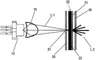
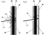
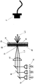
- FIG. 1 is an explanatory diagram showing a configuration of a light source device according to the first embodiment of the present invention.
- This light source device has an excitation light source 10 that emits excitation light L1, and a plate-like shape in which excitation light L1 from the excitation light source 10 is incident on one surface (left surface in the drawing) of the excitation light source 10 in front of the excitation light source 10.
- a wavelength conversion member 20 is provided.
- the excitation light source 10 is arranged so that the direction of the optical axis of the excitation light L1 incident on the wavelength conversion member 20 from the excitation light source 10 is perpendicular to one surface of the wavelength conversion member 20. .
- a wavelength conversion layer 21 made of a phosphor that receives the excitation light L1 from the excitation light source 10 and emits long-wavelength light L2 having a longer wavelength than the excitation light L1 is formed on the translucent plate 22.
- a protective layer (not shown) made of glass, for example, may be provided on the surface of the wavelength conversion layer 21.
- the wavelength conversion member 20 is disposed such that the wavelength conversion layer 21 faces the side opposite to the excitation light source 10 side, and thus, the translucent plate 22 on which the wavelength conversion layer 21 is not formed. Is a surface on which the excitation light L1 from the excitation light source 10 in the wavelength conversion member 20 is incident.
- a plate-like or film-like light reflecting member 30 having an excitation light transmission window 31 that transmits the excitation light L1 from the excitation light source 10 is provided on one side of the wavelength conversion member 20 where the excitation light L1 from the excitation light source 10 is incident. Is provided.
- a plate-like or film-like filter member 40 is provided on the other surface side of the wavelength conversion member 20.
- a collimator lens 15 that focuses the excitation light L ⁇ b> 1 emitted from the excitation light source 10 is provided between the excitation light source 10 and the light reflecting member 30.
- a solid light emitting element such as a light emitting diode or a laser diode can be used.
- a blue laser diode can be preferably used.
- the long wavelength light L2 emitted from the wavelength conversion layer 21 in the wavelength conversion member 20 may be any of red light, green light, and blue light, but is preferably green light.
- the phosphor constituting the wavelength conversion layer 21 can be appropriately selected according to the wavelength of the excitation light L1 emitted from the excitation light source 10 and the wavelength of the light emitted from the wavelength conversion layer 21, for example, blue
- the wavelength conversion layer 21 that receives the excitation light L1 from the excitation light source 10 made of a light emitting diode and emits green light is formed, the chemical and thermal stability is high, and the humidity environment and the temperature environment change.
- it is preferable to use a ⁇ sialon green phosphor because the change in the fluorescence characteristics is small and the deterioration is difficult.
- the thickness of the wavelength conversion layer 21 is preferably 50 to 100 ⁇ m. When this thickness is too small, when the excitation light source 10 passes through the wavelength conversion layer 21, the probability of absorption / wavelength conversion is reduced, and the excitation light L ⁇ b> 1 is between the filter member 40 and the light reflection member 30. Since the mutual reflection is repeated, the radiation region from the wavelength conversion layer 21 is expanded, the luminance as the light source is lowered, and a sufficient amount of light as the projector device cannot be obtained. On the other hand, when this thickness is excessive, when the wavelength conversion member 20 receives a thermal history due to the excitation light L1, the thermal expansion of the material constituting the light transmitting plate 22 and the material constituting the wavelength conversion layer 21 is achieved.
- the wavelength conversion layer 21 When stress due to the difference in rate occurs, a crack is generated in the wavelength conversion layer 21, and the wavelength conversion layer 21 may absorb water due to the crack and the light emission characteristics may be deteriorated. Further, in the case of the transmission type configuration as shown in FIG. 1, since the light transmitted through the wavelength conversion member 20 is reduced, the long-wavelength light L2 emitted from the wavelength conversion layer 21 is the wavelength of the light reflection member 30. The amount of repeated mutual reflection with the conversion member 20 increases, the amount of absorption by the light reflection member 30 and the wavelength conversion member 20 increases, and the luminance as a light source also decreases.
- a method of forming the wavelength conversion layer 21 there is a method in which a mixed liquid containing a binder and a phosphor is applied to the surface of the light transmitting plate 22 and dried, and then sintered at a temperature of 650 to 700 ° C., for example.
- the phosphor particles are exposed on the surface, resulting in an uneven scattering surface.
- a gel film is formed by performing a hydrolysis / polycondensation reaction.
- a sol-gel method for firing the gel film, a vapor deposition method for vapor-depositing a phosphor on the surface of the light-transmitting plate 22, and the like are suitable.
- the wavelength conversion layer 21 formed by these methods is preferable because it has an optically flat surface and the filter member 40 can be directly formed on the surface. Thereby, the wavelength conversion layer 21 having a uniform thickness can be obtained, and another optical layer can be formed on the wavelength conversion layer 21.
- the translucent plate 22 one that transmits both the excitation light L ⁇ b> 1 emitted from the excitation light source 10 and the long wavelength light L ⁇ b> 2 emitted from the wavelength conversion layer 21, for example, made of glass such as quartz glass is used. it can.
- the thickness of the light transmitting plate 22 is, for example, 0.6 to 1.5 mm, although it depends on the size. Basically, in order to suppress the spread of light due to mutual reflection of the excitation light L1 and the long wavelength light L2, it is preferable that the thickness of the translucent plate 22 is thin.
- the light reflecting member 30 is not particularly limited as long as it reflects both the excitation light L1 emitted from the excitation light source 10 and the long wavelength light L2 emitted from the wavelength conversion layer 21.
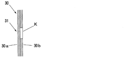
- a material made of a highly light reflective metal can be used, when a blue laser diode is used as the excitation light source 10 and a phosphor that emits green light is used as the wavelength conversion layer 21, as shown in FIG.
- the dielectric multilayer film 30a reflects the blue light in the wavelength range for example 420 ⁇ 470 nm, which is composed of TiO 2 and SiO 2, the green light in the wavelength range for example 490 ⁇ 560 nm
- a light reflecting member 30 can be formed by, for example, a vapor deposition method.
- the light reflecting member 30 may be provided integrally with the wavelength conversion member 20 or may be provided separately from the wavelength conversion member 20.
- the excitation light transmission window 31 of the light reflecting member 30 is not particularly limited as long as it transmits the excitation light L1.
- the excitation light transmission window 31 may be formed of an opening or a material that transmits the excitation light L1.
- the light reflecting member 30 is constituted by a laminate of the dielectric multilayer film 30a that reflects blue light and the dielectric multilayer film 30b that reflects green light
- FIG. As shown in FIG. 2, when an excitation light transmitting window opening K is formed in the dielectric multilayer film 30a that reflects blue light, and a dielectric multilayer film 30b that reflects green light is used that transmits blue light.
- the long wavelength light L2 emitted from the wavelength conversion layer 21 is reflected by the dielectric multilayer film 30b in the excitation light transmission window 31, the long wavelength light L2 is transmitted from the excitation light transmission window 31. Leakage is prevented, and thus higher luminous efficiency can be obtained for the long wavelength light L2 emitted from the wavelength conversion layer 21.
- the filter member 40 reflects the excitation light L1 emitted from the excitation light source 10 and transmits the long wavelength light L2 emitted from the wavelength conversion layer 21.
- a member made of a dielectric multilayer film composed of TiO 2 and SiO 2 can be used as the filter member 40.
- Such a filter member 40 can be formed by, for example, a vapor deposition method.
- the filter member 40 may be provided integrally with the wavelength conversion member 20 or may be provided separately from the wavelength conversion member 20.
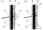
- the excitation light L1 emitted from the excitation light source 10 is focused on the collimator lens 15 and then passed through the excitation light transmission window 31 of the light reflecting member 30 as shown in FIG.
- the light is incident on one surface of the wavelength conversion member 20 (one surface of the translucent plate 22 in the illustrated example).
- the long wavelength light L2 having a longer wavelength than the excitation light L1 is emitted from the wavelength conversion layer 21.
- the light traveling toward the filter member 40 is emitted to the outside through the filter member 40, and the light traveling toward the light reflecting member 30 is reflected by the light reflecting member 30.
- the light is radiated to the outside through the wavelength conversion member 20 and the filter member 40.
- the excitation light L1 transmitted through the wavelength conversion layer 21 is reflected by the filter member 40 and then incident on the wavelength conversion layer 21 as shown in FIG.
- the excitation light L1 radiated from the long wavelength light and further transmitted through the wavelength conversion layer 21 is reflected by the light reflecting member 30, and then enters the wavelength conversion layer 21.
- the long wavelength light is emitted from the wavelength conversion layer 21. Light is emitted.
- the excitation light L1 is reflected by the filter member 40 or the light reflecting member 30.
- the excitation light L1 can be converted into the long-wavelength light L2 with high efficiency, and therefore light of a required wavelength can be emitted with high efficiency.
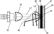
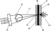
- FIG. 4 is an explanatory diagram showing the configuration of the light source device according to the second embodiment of the present invention.
- This light source device has an excitation light source 10 that emits excitation light L1, and a plate-like shape in which excitation light L1 from the excitation light source 10 is incident on one surface (left surface in the drawing) of the excitation light source 10 in front of the excitation light source 10.
- a wavelength conversion member 20 is provided.
- the excitation light source 10 is arranged such that the direction of the optical axis of the excitation light L1 incident on the wavelength conversion member 20 from the excitation light source 10 is perpendicular to one surface of the wavelength conversion member 20.
- a wavelength conversion layer 21 made of a phosphor that receives the excitation light L1 from the excitation light source 10 and emits long-wavelength light L2 having a longer wavelength than the excitation light L1 is formed on the translucent plate 22.
- a protective layer (not shown) made of glass, for example, may be provided on the surface of the wavelength conversion layer 21.
- the wavelength conversion member 20 is arranged such that the wavelength conversion layer 21 faces the side opposite to the excitation light source 10 side, and thus the light transmitting plate on which the wavelength conversion layer 21 is not formed.
- the surface 22 is a surface on which the excitation light L1 from the excitation light source 10 in the wavelength conversion member 20 is incident.
- a plate-like or film-like filter member 40 that reflects L1 and transmits the long-wavelength light L2 emitted from the wavelength conversion layer 21 is provided.
- a plate-like or film-like light reflecting member 30 is provided on the other surface side of the wavelength conversion member 20.
- a collimator lens 15 that focuses the excitation light L ⁇ b> 1 emitted from the excitation light source 10 is provided between the excitation light source 10 and the filter member 40.
- the plate-like wavelength-selective mirror 45 that transmits the excitation light L1 from the excitation light source 10 and reflects the long-wavelength light L2 emitted from the wavelength conversion layer 21 is disposed between the wavelength conversion member 20 and For example, it is arranged in a state inclined at 45 degrees.
- the excitation light source 10 and the wavelength conversion member 20 the thing of the structure similar to the light source device which concerns on 1st Embodiment can be used.
- a material which comprises the light reflection member 30 and the filter member 40 the thing similar to the light source device which concerns on 1st Embodiment can be used.
- the excitation light transmission window 41 of the filter member 40 is not particularly limited as long as it transmits the excitation light L1.
- it can be formed by an opening or a material that transmits both the excitation light L1 and the long wavelength light L2.
- the wavelength selective mirror 45 a mirror made of a dielectric multilayer film made of TiO 2 and SiO 2 can be used.
- the excitation light L1 emitted from the excitation light source 10 is focused on the collimator lens 15 and further transmitted through the wavelength selective mirror 45, and then, as shown in FIG.
- the light is incident on one surface of the wavelength conversion member 20 (one surface of the light transmitting plate 22 in the illustrated example) through the excitation light transmitting window 41.
- the long wavelength light L2 having a longer wavelength than the excitation light L1 is emitted from the wavelength conversion layer 21.
- the long wavelength light L 2 the light traveling toward the filter member 40 is transmitted through the filter member 40, and further radiated to the outside by being reflected by the wavelength selective mirror 45, toward the light reflecting member 30.
- the light traveling forward is reflected by the light reflecting member 30, then passes through the wavelength conversion member 20 and the filter member 40, and is further reflected by the wavelength selective mirror 45 to be emitted to the outside.
- the excitation light L1 transmitted through the wavelength conversion layer 21 is reflected by the light reflecting member 30 and then incident on the wavelength conversion layer 21 as shown in FIG. Then, after the long wavelength light is emitted from the excitation light L1 transmitted through the wavelength conversion layer 21 and reflected by the filter member 40, the excitation light L1 is incident on the wavelength conversion layer 21. Light is emitted.
- the excitation light L1 is reflected by the light reflecting member 30 or the filter member 40.
- the light is again incident on the wavelength conversion layer 21, so that the excitation light L1 from the excitation light source 10 can be converted into the long wavelength light L2 with high efficiency, and therefore light of a required wavelength is emitted with high efficiency. be able to.
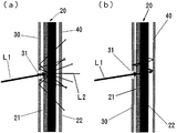
- FIG. 6 is an explanatory diagram showing a configuration of a light source device according to the third embodiment of the present invention.
- the excitation light source is arranged so that the optical axis of the excitation light L1 from the excitation light source 10 is incident on one surface of the wavelength conversion member 20 from a direction inclined with respect to the normal direction of the one surface of the wavelength conversion member 20.
- the light source device according to the third embodiment has the same configuration as the light source device according to the first embodiment.
- the angle formed by the optical axis of the excitation light L1 incident on one surface of the wavelength conversion member 20 and the normal line of one surface of the wavelength conversion member 20 is 3 to 10 °. Is preferred.
- the same effect as the light source device according to the first embodiment can be obtained, and the following effect can be obtained. That is, the excitation light L1 that has passed through the excitation light transmission window 31 of the light reflecting member 30 is incident on one surface of the wavelength conversion member 20 from the direction in which the optical axis is inclined with respect to the normal direction of the one surface of the wavelength conversion member 20. As a result, when the excitation light L1 transmitted through the wavelength conversion layer 21 is reflected by the filter member 40, the reflection angle becomes larger than 0 °, so that the excitation light L1 reflected by the filter member 40 is again transmitted. Since leakage from the excitation light transmission window 31 of the light reflecting member 30 when transmitted through the wavelength conversion layer 21 is prevented or suppressed, higher luminous efficiency can be obtained.
- the wavelength conversion member 20 has the wavelength conversion layer 20 with the wavelength conversion layer 21 facing the excitation light source 10 side.
- the surface of the wavelength conversion layer 21 may be a surface on which the excitation light L1 from the excitation light source is incident.
- the excitation light source 10 includes the wavelength conversion member 20 from a direction in which the optical axis of the excitation light L1 from the excitation light source 10 is inclined with respect to the normal direction of one surface of the wavelength conversion member 20. It may be arranged to be incident on one surface. According to such a configuration, the same effect as that of the light source device according to the third embodiment, that is, when the excitation light L1 transmitted through the wavelength conversion layer 21 is reflected by the light reflecting member 30, the reflection angle thereof is Since it is greater than 0 °, the excitation light L1 reflected by the light reflecting member 30 is prevented or suppressed from leaking from the excitation light transmitting window 41 of the filter member 40 when the excitation light L1 is transmitted through the wavelength conversion layer 21 again. Therefore, higher luminous efficiency can be obtained.
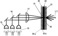
- a plurality of excitation light sources 10 may be provided, and the excitation light source 10 emits light from the excitation light source L ⁇ b> 1 emitted from the excitation light source 10.
- the axis is arranged so as to intersect the normal direction of one surface of the wavelength conversion member 20 at, for example, 90 °, and is emitted from the excitation light source 10 on the optical path of the excitation light L1 from the excitation light source 10 to the wavelength conversion layer 20.
- a light reflection plate 16 that reflects the excitation light L1 toward the wavelength conversion member 20 and a focusing lens 17 that focuses the excitation light L1 reflected by the light reflection plate 16 may be provided.
- Excitation light source (10) A total of 12 1 W class blue laser diodes (with a peak wavelength of 445 nm) were arranged as the excitation light source (10).
- Light reflecting member (30) By depositing silver on one surface of the wavelength conversion member (20) where the wavelength conversion layer (21) is not formed, the thickness of the excitation light transmission window (31) made of a circular opening having a diameter of 1 mm is 1 ⁇ m. A light reflecting member (30) was formed.
- the filter member (40) has a wavelength range of 420 to 480 nm of light reflected by the filter member (40).
- Example 2 A light source device having the same configuration as that of the light source device according to Example 1 was manufactured except that the thickness of the wavelength conversion layer (21) was 95 ⁇ m.
Landscapes
- Physics & Mathematics (AREA)
- General Physics & Mathematics (AREA)
- Optics & Photonics (AREA)
- Chemical & Material Sciences (AREA)
- Engineering & Computer Science (AREA)
- Inorganic Chemistry (AREA)
- Materials Engineering (AREA)
- Organic Chemistry (AREA)
- Multimedia (AREA)
- Non-Portable Lighting Devices Or Systems Thereof (AREA)
- Projection Apparatus (AREA)
- Optical Filters (AREA)
Priority Applications (4)
| Application Number | Priority Date | Filing Date | Title |
|---|---|---|---|
| KR1020137000233A KR101419661B1 (ko) | 2010-08-04 | 2011-07-22 | 광원 장치 |
| US13/813,076 US20130126930A1 (en) | 2010-08-04 | 2011-07-22 | Light source device |
| EP11814468.2A EP2602537B1 (en) | 2010-08-04 | 2011-07-22 | Light source device |
| CN201180038388.9A CN103052841B (zh) | 2010-08-04 | 2011-07-22 | 光源装置 |
Applications Claiming Priority (2)
| Application Number | Priority Date | Filing Date | Title |
|---|---|---|---|
| JP2010175158A JP5257420B2 (ja) | 2010-08-04 | 2010-08-04 | 光源装置 |
| JP2010-175158 | 2010-08-04 |
Publications (1)
| Publication Number | Publication Date |
|---|---|
| WO2012017838A1 true WO2012017838A1 (ja) | 2012-02-09 |
Family
ID=45559344
Family Applications (1)
| Application Number | Title | Priority Date | Filing Date |
|---|---|---|---|
| PCT/JP2011/066671 WO2012017838A1 (ja) | 2010-08-04 | 2011-07-22 | 光源装置 |
Country Status (6)
Cited By (2)
| Publication number | Priority date | Publication date | Assignee | Title |
|---|---|---|---|---|
| CN102830582A (zh) * | 2012-06-04 | 2012-12-19 | 深圳市绎立锐光科技开发有限公司 | 发光装置及其相关投影系统 |
| CN105022217A (zh) * | 2012-03-19 | 2015-11-04 | 深圳市光峰光电技术有限公司 | 照明装置和投影装置 |
Families Citing this family (32)
| Publication number | Priority date | Publication date | Assignee | Title |
|---|---|---|---|---|
| TWI421620B (zh) | 2010-11-03 | 2014-01-01 | Delta Electronics Inc | 光源調整裝置及包含該光源調整裝置之投影系統 |
| CN102466956B (zh) * | 2010-11-11 | 2014-05-28 | 台达电子工业股份有限公司 | 光源调整装置及包含该光源调整装置的投影系统 |
| US9116421B1 (en) * | 2012-01-07 | 2015-08-25 | Greenlight Optics, LLC | Projector with laser illumination elements offset along an offset axis |
| JP6054705B2 (ja) * | 2012-10-24 | 2016-12-27 | スタンレー電気株式会社 | 発光素子と蛍光体を用いた発光装置 |
| US9159890B2 (en) * | 2013-02-15 | 2015-10-13 | Osram Opto Semiconductors Gmbh | Optoelectronic semiconductor component |
| JP5812520B2 (ja) * | 2013-03-28 | 2015-11-17 | ウシオ電機株式会社 | 蛍光光源装置 |
| JP2014203852A (ja) * | 2013-04-01 | 2014-10-27 | 日本電気硝子株式会社 | 波長変換部材及び発光デバイス |
| JP5708698B2 (ja) * | 2013-04-19 | 2015-04-30 | カシオ計算機株式会社 | 蛍光体支持体、光源装置及びプロジェクタ |
| CN104238248B (zh) * | 2013-06-08 | 2016-07-20 | 中强光电股份有限公司 | 光源模块与投影装置 |
| JP2015034866A (ja) * | 2013-08-08 | 2015-02-19 | 日本電気硝子株式会社 | プロジェクター用蛍光ホイール及びプロジェクター用発光デバイス |
| JP2015034867A (ja) * | 2013-08-08 | 2015-02-19 | 日本電気硝子株式会社 | プロジェクター用蛍光ホイール及びプロジェクター用発光デバイス |
| JP6232951B2 (ja) * | 2013-11-08 | 2017-11-22 | 日本電気硝子株式会社 | プロジェクター用蛍光ホイール、その製造方法及びプロジェクター用発光デバイス |
| CN105659160A (zh) * | 2013-11-13 | 2016-06-08 | 日本电气硝子株式会社 | 投影器用荧光轮和投影器用发光器件 |
| JP6318606B2 (ja) * | 2013-12-23 | 2018-05-09 | 株式会社リコー | 波長変換部材及びこの波長変換部材を有する光学系及びこの波長変換部材を有する光源装置及びこの光源装置を有する投影装置 |
| JP6476545B2 (ja) * | 2014-01-22 | 2019-03-06 | 日本電気硝子株式会社 | プロジェクター用蛍光ホイール及びプロジェクター用発光デバイス |
| JP2015166787A (ja) * | 2014-03-04 | 2015-09-24 | カシオ計算機株式会社 | 光源装置及び投影装置 |
| US10732495B2 (en) | 2014-05-02 | 2020-08-04 | Coretronic Corporation | Illumination system, projection apparatus and method for driving illumination system |
| CN105204278B (zh) * | 2014-05-26 | 2017-05-10 | 台达电子工业股份有限公司 | 光源系统及其适用的投影设备 |
| KR101620193B1 (ko) * | 2014-09-26 | 2016-05-12 | 현대자동차주식회사 | 헤드램프용 레이저 광학계 |
| US9915859B2 (en) * | 2015-06-05 | 2018-03-13 | Canon Kabushiki Kaisha | Optical element, light source device using the same, and projection display apparatus |
| JP6179628B2 (ja) * | 2016-03-23 | 2017-08-16 | セイコーエプソン株式会社 | 照明装置、電子機器及び投射型表示装置 |
| US10551031B2 (en) | 2016-05-20 | 2020-02-04 | Sony Corporation | Light source apparatus and projection display apparatus |
| KR102513351B1 (ko) * | 2016-06-30 | 2023-03-23 | 엘지전자 주식회사 | 반도체 발광 소자를 이용한 차량용 램프 |
| CN108663879B (zh) | 2017-03-31 | 2021-04-06 | 中强光电股份有限公司 | 投影机及其照明系统 |
| CN108803213B (zh) * | 2017-04-27 | 2021-03-19 | 中强光电股份有限公司 | 波长转换滤光模块以及照明系统 |
| US11269245B2 (en) * | 2017-08-17 | 2022-03-08 | Sony Corporation | Light source unit and projection display including a phosphor wheel |
| JP6955989B2 (ja) * | 2017-12-13 | 2021-10-27 | 東京エレクトロン株式会社 | 検査装置 |
| CN110703552B (zh) | 2018-07-10 | 2021-10-15 | 中强光电股份有限公司 | 照明系统以及投影装置 |
| CN111123629A (zh) * | 2018-11-01 | 2020-05-08 | 深圳光峰科技股份有限公司 | 波长转换装置及其制备方法、发光装置和投影装置 |
| JP2020160366A (ja) * | 2019-03-27 | 2020-10-01 | パナソニックIpマネジメント株式会社 | 波長変換素子及び照明装置 |
| JP7341740B2 (ja) * | 2019-06-12 | 2023-09-11 | キヤノン株式会社 | 光源装置および画像投射装置 |
| US11714275B1 (en) | 2022-11-25 | 2023-08-01 | Christie Digital Systems Usa, Inc. | Dual phosphor wheel projection system |
Citations (5)
| Publication number | Priority date | Publication date | Assignee | Title |
|---|---|---|---|---|
| JP2002268140A (ja) | 2001-03-08 | 2002-09-18 | Seiko Epson Corp | 投射型カラー表示装置 |
| JP2004341105A (ja) | 2003-05-14 | 2004-12-02 | Nec Viewtechnology Ltd | 投写型表示装置 |
| JP2005347263A (ja) * | 2004-06-04 | 2005-12-15 | Lumileds Lighting Us Llc | 照明装置における離間した波長変換 |
| JP2007200782A (ja) * | 2006-01-27 | 2007-08-09 | Ricoh Opt Ind Co Ltd | 蛍光体光源およびその製造方法および光源装置および照明装置 |
| JP2008116784A (ja) * | 2006-11-07 | 2008-05-22 | Seiko Epson Corp | 光源装置、照明装置、プロジェクタおよびモニタ装置 |
Family Cites Families (12)
| Publication number | Priority date | Publication date | Assignee | Title |
|---|---|---|---|---|
| FR2638271B1 (fr) * | 1988-10-21 | 1990-12-28 | Soc Et Dev Prod Electron | Tableau d'affichage a elements lumineux |
| JP4054594B2 (ja) * | 2002-04-04 | 2008-02-27 | 日東光学株式会社 | 光源装置及びプロジェクタ |
| JP4689190B2 (ja) * | 2004-05-18 | 2011-05-25 | オリンパス株式会社 | 内視鏡装置および内視鏡用アダプタ |
| WO2006038502A1 (ja) * | 2004-10-01 | 2006-04-13 | Nichia Corporation | 発光装置 |
| JP5616000B2 (ja) * | 2004-12-06 | 2014-10-29 | コーニンクレッカ フィリップス エヌ ヴェ | コンパクトな色可変光源としてのシングルチップled |
| JP2007322851A (ja) * | 2006-06-02 | 2007-12-13 | Matsushita Electric Ind Co Ltd | 投射表示装置 |
| EP2064489B1 (en) * | 2006-09-23 | 2019-01-02 | YLX Incorporated | Brightness enhancement method and apparatus of light emitting diodes |
| DE102006046199A1 (de) * | 2006-09-29 | 2008-04-03 | Osram Opto Semiconductors Gmbh | Optoelektronisches Bauelement |
| JP2009069550A (ja) * | 2007-09-14 | 2009-04-02 | Kimoto & Co Ltd | 情報表示部材 |
| US8096668B2 (en) * | 2008-01-16 | 2012-01-17 | Abu-Ageel Nayef M | Illumination systems utilizing wavelength conversion materials |
| CN101498415B (zh) * | 2008-01-30 | 2011-01-26 | 绎立锐光科技开发(深圳)有限公司 | 基于荧光粉提高混合光出射效率的光源及其方法 |
| CN101539270B (zh) * | 2008-03-17 | 2011-06-08 | 绎立锐光科技开发(深圳)有限公司 | 具有发射角度选择特性的光波长转换方法 |
-
2010
- 2010-08-04 JP JP2010175158A patent/JP5257420B2/ja active Active
-
2011
- 2011-07-22 EP EP11814468.2A patent/EP2602537B1/en active Active
- 2011-07-22 CN CN201180038388.9A patent/CN103052841B/zh active Active
- 2011-07-22 US US13/813,076 patent/US20130126930A1/en not_active Abandoned
- 2011-07-22 KR KR1020137000233A patent/KR101419661B1/ko active Active
- 2011-07-22 WO PCT/JP2011/066671 patent/WO2012017838A1/ja active Application Filing
Patent Citations (5)
| Publication number | Priority date | Publication date | Assignee | Title |
|---|---|---|---|---|
| JP2002268140A (ja) | 2001-03-08 | 2002-09-18 | Seiko Epson Corp | 投射型カラー表示装置 |
| JP2004341105A (ja) | 2003-05-14 | 2004-12-02 | Nec Viewtechnology Ltd | 投写型表示装置 |
| JP2005347263A (ja) * | 2004-06-04 | 2005-12-15 | Lumileds Lighting Us Llc | 照明装置における離間した波長変換 |
| JP2007200782A (ja) * | 2006-01-27 | 2007-08-09 | Ricoh Opt Ind Co Ltd | 蛍光体光源およびその製造方法および光源装置および照明装置 |
| JP2008116784A (ja) * | 2006-11-07 | 2008-05-22 | Seiko Epson Corp | 光源装置、照明装置、プロジェクタおよびモニタ装置 |
Non-Patent Citations (1)
| Title |
|---|
| See also references of EP2602537A4 |
Cited By (3)
| Publication number | Priority date | Publication date | Assignee | Title |
|---|---|---|---|---|
| CN105022217A (zh) * | 2012-03-19 | 2015-11-04 | 深圳市光峰光电技术有限公司 | 照明装置和投影装置 |
| CN102830582A (zh) * | 2012-06-04 | 2012-12-19 | 深圳市绎立锐光科技开发有限公司 | 发光装置及其相关投影系统 |
| WO2013181903A1 (zh) * | 2012-06-04 | 2013-12-12 | 深圳市绎立锐光科技开发有限公司 | 发光装置及其相关投影系统 |
Also Published As
| Publication number | Publication date |
|---|---|
| KR20130031878A (ko) | 2013-03-29 |
| EP2602537A1 (en) | 2013-06-12 |
| EP2602537B1 (en) | 2018-02-28 |
| KR101419661B1 (ko) | 2014-07-15 |
| EP2602537A4 (en) | 2014-11-12 |
| US20130126930A1 (en) | 2013-05-23 |
| JP5257420B2 (ja) | 2013-08-07 |
| CN103052841B (zh) | 2015-02-11 |
| CN103052841A (zh) | 2013-04-17 |
| JP2012038452A (ja) | 2012-02-23 |
Similar Documents
| Publication | Publication Date | Title |
|---|---|---|
| JP5257420B2 (ja) | 光源装置 | |
| CN103503178B (zh) | 光学元件以及利用了该光学元件的半导体发光装置 | |
| US10477166B2 (en) | Wavelength conversion device and projector | |
| WO2018074132A1 (ja) | 波長変換部材、発光デバイス及び波長変換部材の製造方法 | |
| CN107017326B (zh) | 转换装置 | |
| EP2525703B1 (en) | Phosphor device and lighting apparatus comprising the same | |
| JP2017027019A (ja) | 光源装置 | |
| KR101817828B1 (ko) | 옵티칼 휠 | |
| CN105423238A (zh) | 波长变换部件、发光装置、投影机、以及波长变换部件的制造方法 | |
| JPWO2015072319A1 (ja) | プロジェクター用蛍光ホイール及びプロジェクター用発光デバイス | |
| JP2012243701A (ja) | 光源装置および照明装置 | |
| CN104851959B (zh) | 光转换基板、发光封装件以及包括其的汽车车灯 | |
| US20170052362A1 (en) | Phosphor wheel and wavelength converting device applying the same | |
| TW201636542A (zh) | 經光學增強之固態光轉換器 | |
| TW202432794A (zh) | 波長轉換元件、製造其之方法、光轉換裝置、及產生白光的方法 | |
| CN106468427A (zh) | 荧光色轮与应用其的波长转换装置 | |
| JP2014203852A (ja) | 波長変換部材及び発光デバイス | |
| US10808893B2 (en) | Optoelectronic semiconductor light source and Bragg mirror | |
| TWI677648B (zh) | 光波長轉換裝置 | |
| CN105841097A (zh) | 光波长转换装置及其适用的光源系统 | |
| JP2007258466A (ja) | 照明装置及び発光装置 | |
| WO2017043121A1 (ja) | 発光装置および照明装置 | |
| CN110050223B (zh) | 光转换器件 | |
| JP5648676B2 (ja) | 光源装置 | |
| WO2021157738A1 (ja) | 光学装置 |
Legal Events
| Date | Code | Title | Description |
|---|---|---|---|
| WWE | Wipo information: entry into national phase |
Ref document number: 201180038388.9 Country of ref document: CN |
|
| 121 | Ep: the epo has been informed by wipo that ep was designated in this application |
Ref document number: 11814468 Country of ref document: EP Kind code of ref document: A1 |
|
| ENP | Entry into the national phase |
Ref document number: 20137000233 Country of ref document: KR Kind code of ref document: A |
|
| WWE | Wipo information: entry into national phase |
Ref document number: 13813076 Country of ref document: US |
|
| NENP | Non-entry into the national phase |
Ref country code: DE |
|
| WWE | Wipo information: entry into national phase |
Ref document number: 2011814468 Country of ref document: EP |