WO2012002233A1 - Procédé de production de dispositif à capteur et dispositif à capteur - Google Patents
Procédé de production de dispositif à capteur et dispositif à capteur Download PDFInfo
- Publication number
- WO2012002233A1 WO2012002233A1 PCT/JP2011/064313 JP2011064313W WO2012002233A1 WO 2012002233 A1 WO2012002233 A1 WO 2012002233A1 JP 2011064313 W JP2011064313 W JP 2011064313W WO 2012002233 A1 WO2012002233 A1 WO 2012002233A1
- Authority
- WO
- WIPO (PCT)
- Prior art keywords
- sensor
- resin
- metal electrodes
- sensor device
- electrode
- Prior art date
Links
- 238000000034 method Methods 0.000 title claims abstract description 37
- 229920005989 resin Polymers 0.000 claims abstract description 218
- 239000011347 resin Substances 0.000 claims abstract description 218
- 229910052751 metal Inorganic materials 0.000 claims abstract description 79
- 239000002184 metal Substances 0.000 claims abstract description 79
- 239000000758 substrate Substances 0.000 claims abstract description 68
- 238000004519 manufacturing process Methods 0.000 claims description 38
- 238000000926 separation method Methods 0.000 claims description 35
- XUIMIQQOPSSXEZ-UHFFFAOYSA-N Silicon Chemical compound [Si] XUIMIQQOPSSXEZ-UHFFFAOYSA-N 0.000 claims description 26
- 239000010703 silicon Substances 0.000 claims description 26
- 229910052710 silicon Inorganic materials 0.000 claims description 26
- 239000000463 material Substances 0.000 claims description 25
- 238000005260 corrosion Methods 0.000 abstract description 8
- 230000007797 corrosion Effects 0.000 abstract description 8
- 239000012080 ambient air Substances 0.000 abstract 1
- 230000000694 effects Effects 0.000 abstract 1
- 238000004382 potting Methods 0.000 description 98
- 230000001133 acceleration Effects 0.000 description 66
- 239000003822 epoxy resin Substances 0.000 description 28
- 229920000647 polyepoxide Polymers 0.000 description 28
- 239000004065 semiconductor Substances 0.000 description 18
- 238000010521 absorption reaction Methods 0.000 description 14
- XLYOFNOQVPJJNP-UHFFFAOYSA-N water Substances O XLYOFNOQVPJJNP-UHFFFAOYSA-N 0.000 description 14
- 230000008569 process Effects 0.000 description 11
- 238000005259 measurement Methods 0.000 description 9
- 238000000576 coating method Methods 0.000 description 8
- 238000005452 bending Methods 0.000 description 7
- 230000015572 biosynthetic process Effects 0.000 description 6
- 238000005304 joining Methods 0.000 description 6
- 229920001721 polyimide Polymers 0.000 description 6
- 239000009719 polyimide resin Substances 0.000 description 6
- 238000003892 spreading Methods 0.000 description 6
- 230000007480 spreading Effects 0.000 description 6
- 239000004925 Acrylic resin Substances 0.000 description 5
- 229920000178 Acrylic resin Polymers 0.000 description 5
- 238000006073 displacement reaction Methods 0.000 description 5
- 229920002803 thermoplastic polyurethane Polymers 0.000 description 4
- 239000000853 adhesive Substances 0.000 description 3
- 230000001070 adhesive effect Effects 0.000 description 3
- 230000008859 change Effects 0.000 description 3
- 239000011248 coating agent Substances 0.000 description 3
- 238000001514 detection method Methods 0.000 description 3
- 238000005530 etching Methods 0.000 description 3
- 238000000059 patterning Methods 0.000 description 3
- 230000002093 peripheral effect Effects 0.000 description 3
- 238000007789 sealing Methods 0.000 description 3
- 230000035945 sensitivity Effects 0.000 description 3
- 229910000838 Al alloy Inorganic materials 0.000 description 2
- PXHVJJICTQNCMI-UHFFFAOYSA-N Nickel Chemical compound [Ni] PXHVJJICTQNCMI-UHFFFAOYSA-N 0.000 description 2
- KDLHZDBZIXYQEI-UHFFFAOYSA-N Palladium Chemical compound [Pd] KDLHZDBZIXYQEI-UHFFFAOYSA-N 0.000 description 2
- VYPSYNLAJGMNEJ-UHFFFAOYSA-N Silicium dioxide Chemical compound O=[Si]=O VYPSYNLAJGMNEJ-UHFFFAOYSA-N 0.000 description 2
- 230000002411 adverse Effects 0.000 description 2
- 239000004020 conductor Substances 0.000 description 2
- 238000000708 deep reactive-ion etching Methods 0.000 description 2
- 239000010931 gold Substances 0.000 description 2
- 239000011810 insulating material Substances 0.000 description 2
- 239000007769 metal material Substances 0.000 description 2
- 229920002050 silicone resin Polymers 0.000 description 2
- 229910018125 Al-Si Inorganic materials 0.000 description 1
- 229910018520 Al—Si Inorganic materials 0.000 description 1
- RYGMFSIKBFXOCR-UHFFFAOYSA-N Copper Chemical compound [Cu] RYGMFSIKBFXOCR-UHFFFAOYSA-N 0.000 description 1
- 229930182556 Polyacetal Natural products 0.000 description 1
- 229910018594 Si-Cu Inorganic materials 0.000 description 1
- 229910004298 SiO 2 Inorganic materials 0.000 description 1
- BQCADISMDOOEFD-UHFFFAOYSA-N Silver Chemical compound [Ag] BQCADISMDOOEFD-UHFFFAOYSA-N 0.000 description 1
- 229910008465 Si—Cu Inorganic materials 0.000 description 1
- 229910052782 aluminium Inorganic materials 0.000 description 1
- XAGFODPZIPBFFR-UHFFFAOYSA-N aluminium Chemical compound [Al] XAGFODPZIPBFFR-UHFFFAOYSA-N 0.000 description 1
- 229910052802 copper Inorganic materials 0.000 description 1
- 239000010949 copper Substances 0.000 description 1
- 238000010586 diagram Methods 0.000 description 1
- 238000005516 engineering process Methods 0.000 description 1
- -1 for example Inorganic materials 0.000 description 1
- 239000011521 glass Substances 0.000 description 1
- PCHJSUWPFVWCPO-UHFFFAOYSA-N gold Chemical compound [Au] PCHJSUWPFVWCPO-UHFFFAOYSA-N 0.000 description 1
- 229910052737 gold Inorganic materials 0.000 description 1
- 239000011256 inorganic filler Substances 0.000 description 1
- 229910003475 inorganic filler Inorganic materials 0.000 description 1
- 150000002739 metals Chemical class 0.000 description 1
- 229910052759 nickel Inorganic materials 0.000 description 1
- 239000011368 organic material Substances 0.000 description 1
- 230000003204 osmotic effect Effects 0.000 description 1
- 229910052763 palladium Inorganic materials 0.000 description 1
- 230000000149 penetrating effect Effects 0.000 description 1
- 230000035515 penetration Effects 0.000 description 1
- 239000013500 performance material Substances 0.000 description 1
- 239000005011 phenolic resin Substances 0.000 description 1
- 229920000515 polycarbonate Polymers 0.000 description 1
- 239000004417 polycarbonate Substances 0.000 description 1
- 229920000728 polyester Polymers 0.000 description 1
- 229920006324 polyoxymethylene Polymers 0.000 description 1
- 230000009467 reduction Effects 0.000 description 1
- 230000004044 response Effects 0.000 description 1
- 239000000377 silicon dioxide Substances 0.000 description 1
- 229910052709 silver Inorganic materials 0.000 description 1
- 239000004332 silver Substances 0.000 description 1
- 238000003860 storage Methods 0.000 description 1
- 239000000126 substance Substances 0.000 description 1
- 239000000454 talc Substances 0.000 description 1
- 229910052623 talc Inorganic materials 0.000 description 1
Images


Classifications
-
- H—ELECTRICITY
- H01—ELECTRIC ELEMENTS
- H01L—SEMICONDUCTOR DEVICES NOT COVERED BY CLASS H10
- H01L29/00—Semiconductor devices adapted for rectifying, amplifying, oscillating or switching, or capacitors or resistors with at least one potential-jump barrier or surface barrier, e.g. PN junction depletion layer or carrier concentration layer; Details of semiconductor bodies or of electrodes thereof ; Multistep manufacturing processes therefor
- H01L29/66—Types of semiconductor device ; Multistep manufacturing processes therefor
- H01L29/84—Types of semiconductor device ; Multistep manufacturing processes therefor controllable by variation of applied mechanical force, e.g. of pressure
-
- B—PERFORMING OPERATIONS; TRANSPORTING
- B81—MICROSTRUCTURAL TECHNOLOGY
- B81B—MICROSTRUCTURAL DEVICES OR SYSTEMS, e.g. MICROMECHANICAL DEVICES
- B81B7/00—Microstructural systems; Auxiliary parts of microstructural devices or systems
- B81B7/0009—Structural features, others than packages, for protecting a device against environmental influences
- B81B7/0025—Protection against chemical alteration
-
- B—PERFORMING OPERATIONS; TRANSPORTING
- B81—MICROSTRUCTURAL TECHNOLOGY
- B81B—MICROSTRUCTURAL DEVICES OR SYSTEMS, e.g. MICROMECHANICAL DEVICES
- B81B7/00—Microstructural systems; Auxiliary parts of microstructural devices or systems
- B81B7/0032—Packages or encapsulation
- B81B7/0045—Packages or encapsulation for reducing stress inside of the package structure
- B81B7/0054—Packages or encapsulation for reducing stress inside of the package structure between other parts not provided for in B81B7/0048 - B81B7/0051
-
- B—PERFORMING OPERATIONS; TRANSPORTING
- B81—MICROSTRUCTURAL TECHNOLOGY
- B81B—MICROSTRUCTURAL DEVICES OR SYSTEMS, e.g. MICROMECHANICAL DEVICES
- B81B7/00—Microstructural systems; Auxiliary parts of microstructural devices or systems
- B81B7/0032—Packages or encapsulation
- B81B7/007—Interconnections between the MEMS and external electrical signals
-
- G—PHYSICS
- G01—MEASURING; TESTING
- G01P—MEASURING LINEAR OR ANGULAR SPEED, ACCELERATION, DECELERATION, OR SHOCK; INDICATING PRESENCE, ABSENCE, OR DIRECTION, OF MOVEMENT
- G01P15/00—Measuring acceleration; Measuring deceleration; Measuring shock, i.e. sudden change of acceleration
- G01P15/02—Measuring acceleration; Measuring deceleration; Measuring shock, i.e. sudden change of acceleration by making use of inertia forces using solid seismic masses
- G01P15/08—Measuring acceleration; Measuring deceleration; Measuring shock, i.e. sudden change of acceleration by making use of inertia forces using solid seismic masses with conversion into electric or magnetic values
- G01P15/0802—Details
-
- G—PHYSICS
- G01—MEASURING; TESTING
- G01P—MEASURING LINEAR OR ANGULAR SPEED, ACCELERATION, DECELERATION, OR SHOCK; INDICATING PRESENCE, ABSENCE, OR DIRECTION, OF MOVEMENT
- G01P15/00—Measuring acceleration; Measuring deceleration; Measuring shock, i.e. sudden change of acceleration
- G01P15/02—Measuring acceleration; Measuring deceleration; Measuring shock, i.e. sudden change of acceleration by making use of inertia forces using solid seismic masses
- G01P15/08—Measuring acceleration; Measuring deceleration; Measuring shock, i.e. sudden change of acceleration by making use of inertia forces using solid seismic masses with conversion into electric or magnetic values
- G01P15/12—Measuring acceleration; Measuring deceleration; Measuring shock, i.e. sudden change of acceleration by making use of inertia forces using solid seismic masses with conversion into electric or magnetic values by alteration of electrical resistance
- G01P15/123—Measuring acceleration; Measuring deceleration; Measuring shock, i.e. sudden change of acceleration by making use of inertia forces using solid seismic masses with conversion into electric or magnetic values by alteration of electrical resistance by piezo-resistive elements, e.g. semiconductor strain gauges
-
- H—ELECTRICITY
- H01—ELECTRIC ELEMENTS
- H01L—SEMICONDUCTOR DEVICES NOT COVERED BY CLASS H10
- H01L21/00—Processes or apparatus adapted for the manufacture or treatment of semiconductor or solid state devices or of parts thereof
- H01L21/02—Manufacture or treatment of semiconductor devices or of parts thereof
-
- H—ELECTRICITY
- H01—ELECTRIC ELEMENTS
- H01L—SEMICONDUCTOR DEVICES NOT COVERED BY CLASS H10
- H01L24/00—Arrangements for connecting or disconnecting semiconductor or solid-state bodies; Methods or apparatus related thereto
- H01L24/01—Means for bonding being attached to, or being formed on, the surface to be connected, e.g. chip-to-package, die-attach, "first-level" interconnects; Manufacturing methods related thereto
- H01L24/42—Wire connectors; Manufacturing methods related thereto
- H01L24/47—Structure, shape, material or disposition of the wire connectors after the connecting process
- H01L24/48—Structure, shape, material or disposition of the wire connectors after the connecting process of an individual wire connector
-
- H—ELECTRICITY
- H01—ELECTRIC ELEMENTS
- H01L—SEMICONDUCTOR DEVICES NOT COVERED BY CLASS H10
- H01L24/00—Arrangements for connecting or disconnecting semiconductor or solid-state bodies; Methods or apparatus related thereto
- H01L24/01—Means for bonding being attached to, or being formed on, the surface to be connected, e.g. chip-to-package, die-attach, "first-level" interconnects; Manufacturing methods related thereto
- H01L24/42—Wire connectors; Manufacturing methods related thereto
- H01L24/47—Structure, shape, material or disposition of the wire connectors after the connecting process
- H01L24/49—Structure, shape, material or disposition of the wire connectors after the connecting process of a plurality of wire connectors
-
- H—ELECTRICITY
- H01—ELECTRIC ELEMENTS
- H01L—SEMICONDUCTOR DEVICES NOT COVERED BY CLASS H10
- H01L24/00—Arrangements for connecting or disconnecting semiconductor or solid-state bodies; Methods or apparatus related thereto
- H01L24/80—Methods for connecting semiconductor or other solid state bodies using means for bonding being attached to, or being formed on, the surface to be connected
- H01L24/85—Methods for connecting semiconductor or other solid state bodies using means for bonding being attached to, or being formed on, the surface to be connected using a wire connector
-
- B—PERFORMING OPERATIONS; TRANSPORTING
- B81—MICROSTRUCTURAL TECHNOLOGY
- B81B—MICROSTRUCTURAL DEVICES OR SYSTEMS, e.g. MICROMECHANICAL DEVICES
- B81B2201/00—Specific applications of microelectromechanical systems
- B81B2201/02—Sensors
- B81B2201/0228—Inertial sensors
- B81B2201/0235—Accelerometers
-
- B—PERFORMING OPERATIONS; TRANSPORTING
- B81—MICROSTRUCTURAL TECHNOLOGY
- B81B—MICROSTRUCTURAL DEVICES OR SYSTEMS, e.g. MICROMECHANICAL DEVICES
- B81B2207/00—Microstructural systems or auxiliary parts thereof
- B81B2207/09—Packages
- B81B2207/091—Arrangements for connecting external electrical signals to mechanical structures inside the package
- B81B2207/094—Feed-through, via
- B81B2207/096—Feed-through, via through the substrate
-
- B—PERFORMING OPERATIONS; TRANSPORTING
- B81—MICROSTRUCTURAL TECHNOLOGY
- B81B—MICROSTRUCTURAL DEVICES OR SYSTEMS, e.g. MICROMECHANICAL DEVICES
- B81B2207/00—Microstructural systems or auxiliary parts thereof
- B81B2207/11—Structural features, others than packages, for protecting a device against environmental influences
- B81B2207/115—Protective layers applied directly to the device before packaging
-
- G—PHYSICS
- G01—MEASURING; TESTING
- G01P—MEASURING LINEAR OR ANGULAR SPEED, ACCELERATION, DECELERATION, OR SHOCK; INDICATING PRESENCE, ABSENCE, OR DIRECTION, OF MOVEMENT
- G01P15/00—Measuring acceleration; Measuring deceleration; Measuring shock, i.e. sudden change of acceleration
- G01P15/02—Measuring acceleration; Measuring deceleration; Measuring shock, i.e. sudden change of acceleration by making use of inertia forces using solid seismic masses
- G01P15/08—Measuring acceleration; Measuring deceleration; Measuring shock, i.e. sudden change of acceleration by making use of inertia forces using solid seismic masses with conversion into electric or magnetic values
- G01P2015/0805—Measuring acceleration; Measuring deceleration; Measuring shock, i.e. sudden change of acceleration by making use of inertia forces using solid seismic masses with conversion into electric or magnetic values being provided with a particular type of spring-mass-system for defining the displacement of a seismic mass due to an external acceleration
- G01P2015/0822—Measuring acceleration; Measuring deceleration; Measuring shock, i.e. sudden change of acceleration by making use of inertia forces using solid seismic masses with conversion into electric or magnetic values being provided with a particular type of spring-mass-system for defining the displacement of a seismic mass due to an external acceleration for defining out-of-plane movement of the mass
- G01P2015/084—Measuring acceleration; Measuring deceleration; Measuring shock, i.e. sudden change of acceleration by making use of inertia forces using solid seismic masses with conversion into electric or magnetic values being provided with a particular type of spring-mass-system for defining the displacement of a seismic mass due to an external acceleration for defining out-of-plane movement of the mass the mass being suspended at more than one of its sides, e.g. membrane-type suspension, so as to permit multi-axis movement of the mass
- G01P2015/0842—Measuring acceleration; Measuring deceleration; Measuring shock, i.e. sudden change of acceleration by making use of inertia forces using solid seismic masses with conversion into electric or magnetic values being provided with a particular type of spring-mass-system for defining the displacement of a seismic mass due to an external acceleration for defining out-of-plane movement of the mass the mass being suspended at more than one of its sides, e.g. membrane-type suspension, so as to permit multi-axis movement of the mass the mass being of clover leaf shape
-
- H—ELECTRICITY
- H01—ELECTRIC ELEMENTS
- H01L—SEMICONDUCTOR DEVICES NOT COVERED BY CLASS H10
- H01L2224/00—Indexing scheme for arrangements for connecting or disconnecting semiconductor or solid-state bodies and methods related thereto as covered by H01L24/00
- H01L2224/01—Means for bonding being attached to, or being formed on, the surface to be connected, e.g. chip-to-package, die-attach, "first-level" interconnects; Manufacturing methods related thereto
- H01L2224/02—Bonding areas; Manufacturing methods related thereto
- H01L2224/04—Structure, shape, material or disposition of the bonding areas prior to the connecting process
- H01L2224/04042—Bonding areas specifically adapted for wire connectors, e.g. wirebond pads
-
- H—ELECTRICITY
- H01—ELECTRIC ELEMENTS
- H01L—SEMICONDUCTOR DEVICES NOT COVERED BY CLASS H10
- H01L2224/00—Indexing scheme for arrangements for connecting or disconnecting semiconductor or solid-state bodies and methods related thereto as covered by H01L24/00
- H01L2224/01—Means for bonding being attached to, or being formed on, the surface to be connected, e.g. chip-to-package, die-attach, "first-level" interconnects; Manufacturing methods related thereto
- H01L2224/02—Bonding areas; Manufacturing methods related thereto
- H01L2224/04—Structure, shape, material or disposition of the bonding areas prior to the connecting process
- H01L2224/05—Structure, shape, material or disposition of the bonding areas prior to the connecting process of an individual bonding area
- H01L2224/0554—External layer
- H01L2224/0555—Shape
- H01L2224/05552—Shape in top view
- H01L2224/05554—Shape in top view being square
-
- H—ELECTRICITY
- H01—ELECTRIC ELEMENTS
- H01L—SEMICONDUCTOR DEVICES NOT COVERED BY CLASS H10
- H01L2224/00—Indexing scheme for arrangements for connecting or disconnecting semiconductor or solid-state bodies and methods related thereto as covered by H01L24/00
- H01L2224/01—Means for bonding being attached to, or being formed on, the surface to be connected, e.g. chip-to-package, die-attach, "first-level" interconnects; Manufacturing methods related thereto
- H01L2224/02—Bonding areas; Manufacturing methods related thereto
- H01L2224/04—Structure, shape, material or disposition of the bonding areas prior to the connecting process
- H01L2224/05—Structure, shape, material or disposition of the bonding areas prior to the connecting process of an individual bonding area
- H01L2224/0554—External layer
- H01L2224/05599—Material
- H01L2224/056—Material with a principal constituent of the material being a metal or a metalloid, e.g. boron [B], silicon [Si], germanium [Ge], arsenic [As], antimony [Sb], tellurium [Te] and polonium [Po], and alloys thereof
- H01L2224/05617—Material with a principal constituent of the material being a metal or a metalloid, e.g. boron [B], silicon [Si], germanium [Ge], arsenic [As], antimony [Sb], tellurium [Te] and polonium [Po], and alloys thereof the principal constituent melting at a temperature of greater than or equal to 400°C and less than 950°C
- H01L2224/05624—Aluminium [Al] as principal constituent
-
- H—ELECTRICITY
- H01—ELECTRIC ELEMENTS
- H01L—SEMICONDUCTOR DEVICES NOT COVERED BY CLASS H10
- H01L2224/00—Indexing scheme for arrangements for connecting or disconnecting semiconductor or solid-state bodies and methods related thereto as covered by H01L24/00
- H01L2224/01—Means for bonding being attached to, or being formed on, the surface to be connected, e.g. chip-to-package, die-attach, "first-level" interconnects; Manufacturing methods related thereto
- H01L2224/42—Wire connectors; Manufacturing methods related thereto
- H01L2224/47—Structure, shape, material or disposition of the wire connectors after the connecting process
- H01L2224/48—Structure, shape, material or disposition of the wire connectors after the connecting process of an individual wire connector
- H01L2224/4805—Shape
- H01L2224/4809—Loop shape
- H01L2224/48091—Arched
-
- H—ELECTRICITY
- H01—ELECTRIC ELEMENTS
- H01L—SEMICONDUCTOR DEVICES NOT COVERED BY CLASS H10
- H01L2224/00—Indexing scheme for arrangements for connecting or disconnecting semiconductor or solid-state bodies and methods related thereto as covered by H01L24/00
- H01L2224/01—Means for bonding being attached to, or being formed on, the surface to be connected, e.g. chip-to-package, die-attach, "first-level" interconnects; Manufacturing methods related thereto
- H01L2224/42—Wire connectors; Manufacturing methods related thereto
- H01L2224/47—Structure, shape, material or disposition of the wire connectors after the connecting process
- H01L2224/48—Structure, shape, material or disposition of the wire connectors after the connecting process of an individual wire connector
- H01L2224/484—Connecting portions
- H01L2224/48463—Connecting portions the connecting portion on the bonding area of the semiconductor or solid-state body being a ball bond
- H01L2224/48465—Connecting portions the connecting portion on the bonding area of the semiconductor or solid-state body being a ball bond the other connecting portion not on the bonding area being a wedge bond, i.e. ball-to-wedge, regular stitch
-
- H—ELECTRICITY
- H01—ELECTRIC ELEMENTS
- H01L—SEMICONDUCTOR DEVICES NOT COVERED BY CLASS H10
- H01L2224/00—Indexing scheme for arrangements for connecting or disconnecting semiconductor or solid-state bodies and methods related thereto as covered by H01L24/00
- H01L2224/01—Means for bonding being attached to, or being formed on, the surface to be connected, e.g. chip-to-package, die-attach, "first-level" interconnects; Manufacturing methods related thereto
- H01L2224/42—Wire connectors; Manufacturing methods related thereto
- H01L2224/47—Structure, shape, material or disposition of the wire connectors after the connecting process
- H01L2224/48—Structure, shape, material or disposition of the wire connectors after the connecting process of an individual wire connector
- H01L2224/484—Connecting portions
- H01L2224/4847—Connecting portions the connecting portion on the bonding area of the semiconductor or solid-state body being a wedge bond
- H01L2224/48472—Connecting portions the connecting portion on the bonding area of the semiconductor or solid-state body being a wedge bond the other connecting portion not on the bonding area also being a wedge bond, i.e. wedge-to-wedge
-
- H—ELECTRICITY
- H01—ELECTRIC ELEMENTS
- H01L—SEMICONDUCTOR DEVICES NOT COVERED BY CLASS H10
- H01L2224/00—Indexing scheme for arrangements for connecting or disconnecting semiconductor or solid-state bodies and methods related thereto as covered by H01L24/00
- H01L2224/01—Means for bonding being attached to, or being formed on, the surface to be connected, e.g. chip-to-package, die-attach, "first-level" interconnects; Manufacturing methods related thereto
- H01L2224/42—Wire connectors; Manufacturing methods related thereto
- H01L2224/47—Structure, shape, material or disposition of the wire connectors after the connecting process
- H01L2224/48—Structure, shape, material or disposition of the wire connectors after the connecting process of an individual wire connector
- H01L2224/4899—Auxiliary members for wire connectors, e.g. flow-barriers, reinforcing structures, spacers, alignment aids
- H01L2224/48991—Auxiliary members for wire connectors, e.g. flow-barriers, reinforcing structures, spacers, alignment aids being formed on the semiconductor or solid-state body to be connected
- H01L2224/48992—Reinforcing structures
-
- H—ELECTRICITY
- H01—ELECTRIC ELEMENTS
- H01L—SEMICONDUCTOR DEVICES NOT COVERED BY CLASS H10
- H01L2224/00—Indexing scheme for arrangements for connecting or disconnecting semiconductor or solid-state bodies and methods related thereto as covered by H01L24/00
- H01L2224/01—Means for bonding being attached to, or being formed on, the surface to be connected, e.g. chip-to-package, die-attach, "first-level" interconnects; Manufacturing methods related thereto
- H01L2224/42—Wire connectors; Manufacturing methods related thereto
- H01L2224/47—Structure, shape, material or disposition of the wire connectors after the connecting process
- H01L2224/48—Structure, shape, material or disposition of the wire connectors after the connecting process of an individual wire connector
- H01L2224/4899—Auxiliary members for wire connectors, e.g. flow-barriers, reinforcing structures, spacers, alignment aids
- H01L2224/48996—Auxiliary members for wire connectors, e.g. flow-barriers, reinforcing structures, spacers, alignment aids being formed on an item to be connected not being a semiconductor or solid-state body
- H01L2224/48997—Reinforcing structures
-
- H—ELECTRICITY
- H01—ELECTRIC ELEMENTS
- H01L—SEMICONDUCTOR DEVICES NOT COVERED BY CLASS H10
- H01L2224/00—Indexing scheme for arrangements for connecting or disconnecting semiconductor or solid-state bodies and methods related thereto as covered by H01L24/00
- H01L2224/01—Means for bonding being attached to, or being formed on, the surface to be connected, e.g. chip-to-package, die-attach, "first-level" interconnects; Manufacturing methods related thereto
- H01L2224/42—Wire connectors; Manufacturing methods related thereto
- H01L2224/47—Structure, shape, material or disposition of the wire connectors after the connecting process
- H01L2224/49—Structure, shape, material or disposition of the wire connectors after the connecting process of a plurality of wire connectors
- H01L2224/491—Disposition
- H01L2224/4911—Disposition the connectors being bonded to at least one common bonding area, e.g. daisy chain
- H01L2224/49113—Disposition the connectors being bonded to at least one common bonding area, e.g. daisy chain the connectors connecting different bonding areas on the semiconductor or solid-state body to a common bonding area outside the body, e.g. converging wires
-
- H—ELECTRICITY
- H01—ELECTRIC ELEMENTS
- H01L—SEMICONDUCTOR DEVICES NOT COVERED BY CLASS H10
- H01L2224/00—Indexing scheme for arrangements for connecting or disconnecting semiconductor or solid-state bodies and methods related thereto as covered by H01L24/00
- H01L2224/01—Means for bonding being attached to, or being formed on, the surface to be connected, e.g. chip-to-package, die-attach, "first-level" interconnects; Manufacturing methods related thereto
- H01L2224/42—Wire connectors; Manufacturing methods related thereto
- H01L2224/47—Structure, shape, material or disposition of the wire connectors after the connecting process
- H01L2224/49—Structure, shape, material or disposition of the wire connectors after the connecting process of a plurality of wire connectors
- H01L2224/491—Disposition
- H01L2224/4912—Layout
- H01L2224/49171—Fan-out arrangements
-
- H—ELECTRICITY
- H01—ELECTRIC ELEMENTS
- H01L—SEMICONDUCTOR DEVICES NOT COVERED BY CLASS H10
- H01L2224/00—Indexing scheme for arrangements for connecting or disconnecting semiconductor or solid-state bodies and methods related thereto as covered by H01L24/00
- H01L2224/80—Methods for connecting semiconductor or other solid state bodies using means for bonding being attached to, or being formed on, the surface to be connected
- H01L2224/85—Methods for connecting semiconductor or other solid state bodies using means for bonding being attached to, or being formed on, the surface to be connected using a wire connector
- H01L2224/85909—Post-treatment of the connector or wire bonding area
- H01L2224/8592—Applying permanent coating, e.g. protective coating
-
- H—ELECTRICITY
- H01—ELECTRIC ELEMENTS
- H01L—SEMICONDUCTOR DEVICES NOT COVERED BY CLASS H10
- H01L2224/00—Indexing scheme for arrangements for connecting or disconnecting semiconductor or solid-state bodies and methods related thereto as covered by H01L24/00
- H01L2224/91—Methods for connecting semiconductor or solid state bodies including different methods provided for in two or more of groups H01L2224/80 - H01L2224/90
- H01L2224/92—Specific sequence of method steps
- H01L2224/922—Connecting different surfaces of the semiconductor or solid-state body with connectors of different types
- H01L2224/9222—Sequential connecting processes
- H01L2224/92242—Sequential connecting processes the first connecting process involving a layer connector
- H01L2224/92247—Sequential connecting processes the first connecting process involving a layer connector the second connecting process involving a wire connector
-
- H—ELECTRICITY
- H01—ELECTRIC ELEMENTS
- H01L—SEMICONDUCTOR DEVICES NOT COVERED BY CLASS H10
- H01L2924/00—Indexing scheme for arrangements or methods for connecting or disconnecting semiconductor or solid-state bodies as covered by H01L24/00
- H01L2924/0001—Technical content checked by a classifier
- H01L2924/00014—Technical content checked by a classifier the subject-matter covered by the group, the symbol of which is combined with the symbol of this group, being disclosed without further technical details
-
- H—ELECTRICITY
- H01—ELECTRIC ELEMENTS
- H01L—SEMICONDUCTOR DEVICES NOT COVERED BY CLASS H10
- H01L2924/00—Indexing scheme for arrangements or methods for connecting or disconnecting semiconductor or solid-state bodies as covered by H01L24/00
- H01L2924/01—Chemical elements
- H01L2924/01004—Beryllium [Be]
-
- H—ELECTRICITY
- H01—ELECTRIC ELEMENTS
- H01L—SEMICONDUCTOR DEVICES NOT COVERED BY CLASS H10
- H01L2924/00—Indexing scheme for arrangements or methods for connecting or disconnecting semiconductor or solid-state bodies as covered by H01L24/00
- H01L2924/01—Chemical elements
- H01L2924/01005—Boron [B]
-
- H—ELECTRICITY
- H01—ELECTRIC ELEMENTS
- H01L—SEMICONDUCTOR DEVICES NOT COVERED BY CLASS H10
- H01L2924/00—Indexing scheme for arrangements or methods for connecting or disconnecting semiconductor or solid-state bodies as covered by H01L24/00
- H01L2924/01—Chemical elements
- H01L2924/01006—Carbon [C]
-
- H—ELECTRICITY
- H01—ELECTRIC ELEMENTS
- H01L—SEMICONDUCTOR DEVICES NOT COVERED BY CLASS H10
- H01L2924/00—Indexing scheme for arrangements or methods for connecting or disconnecting semiconductor or solid-state bodies as covered by H01L24/00
- H01L2924/01—Chemical elements
- H01L2924/01013—Aluminum [Al]
-
- H—ELECTRICITY
- H01—ELECTRIC ELEMENTS
- H01L—SEMICONDUCTOR DEVICES NOT COVERED BY CLASS H10
- H01L2924/00—Indexing scheme for arrangements or methods for connecting or disconnecting semiconductor or solid-state bodies as covered by H01L24/00
- H01L2924/01—Chemical elements
- H01L2924/01029—Copper [Cu]
-
- H—ELECTRICITY
- H01—ELECTRIC ELEMENTS
- H01L—SEMICONDUCTOR DEVICES NOT COVERED BY CLASS H10
- H01L2924/00—Indexing scheme for arrangements or methods for connecting or disconnecting semiconductor or solid-state bodies as covered by H01L24/00
- H01L2924/01—Chemical elements
- H01L2924/01033—Arsenic [As]
-
- H—ELECTRICITY
- H01—ELECTRIC ELEMENTS
- H01L—SEMICONDUCTOR DEVICES NOT COVERED BY CLASS H10
- H01L2924/00—Indexing scheme for arrangements or methods for connecting or disconnecting semiconductor or solid-state bodies as covered by H01L24/00
- H01L2924/01—Chemical elements
- H01L2924/01045—Rhodium [Rh]
-
- H—ELECTRICITY
- H01—ELECTRIC ELEMENTS
- H01L—SEMICONDUCTOR DEVICES NOT COVERED BY CLASS H10
- H01L2924/00—Indexing scheme for arrangements or methods for connecting or disconnecting semiconductor or solid-state bodies as covered by H01L24/00
- H01L2924/01—Chemical elements
- H01L2924/01047—Silver [Ag]
-
- H—ELECTRICITY
- H01—ELECTRIC ELEMENTS
- H01L—SEMICONDUCTOR DEVICES NOT COVERED BY CLASS H10
- H01L2924/00—Indexing scheme for arrangements or methods for connecting or disconnecting semiconductor or solid-state bodies as covered by H01L24/00
- H01L2924/01—Chemical elements
- H01L2924/0106—Neodymium [Nd]
-
- H—ELECTRICITY
- H01—ELECTRIC ELEMENTS
- H01L—SEMICONDUCTOR DEVICES NOT COVERED BY CLASS H10
- H01L2924/00—Indexing scheme for arrangements or methods for connecting or disconnecting semiconductor or solid-state bodies as covered by H01L24/00
- H01L2924/01—Chemical elements
- H01L2924/01079—Gold [Au]
-
- H—ELECTRICITY
- H01—ELECTRIC ELEMENTS
- H01L—SEMICONDUCTOR DEVICES NOT COVERED BY CLASS H10
- H01L2924/00—Indexing scheme for arrangements or methods for connecting or disconnecting semiconductor or solid-state bodies as covered by H01L24/00
- H01L2924/10—Details of semiconductor or other solid state devices to be connected
- H01L2924/11—Device type
- H01L2924/14—Integrated circuits
-
- H—ELECTRICITY
- H01—ELECTRIC ELEMENTS
- H01L—SEMICONDUCTOR DEVICES NOT COVERED BY CLASS H10
- H01L2924/00—Indexing scheme for arrangements or methods for connecting or disconnecting semiconductor or solid-state bodies as covered by H01L24/00
- H01L2924/10—Details of semiconductor or other solid state devices to be connected
- H01L2924/146—Mixed devices
- H01L2924/1461—MEMS
-
- H—ELECTRICITY
- H01—ELECTRIC ELEMENTS
- H01L—SEMICONDUCTOR DEVICES NOT COVERED BY CLASS H10
- H01L2924/00—Indexing scheme for arrangements or methods for connecting or disconnecting semiconductor or solid-state bodies as covered by H01L24/00
- H01L2924/30—Technical effects
- H01L2924/35—Mechanical effects
- H01L2924/351—Thermal stress
- H01L2924/3511—Warping
Definitions
- the present invention relates to a method for manufacturing a sensor device having a movable part that is movable by an external force, and the sensor device.
- a sensor having a movable portion that is displaced according to an external force is formed using a semiconductor substrate, and the displacement of the movable portion is detected as a change in an electrical signal indicating acceleration or angular velocity.
- a hollow package in which the semiconductor substrate on which the sensor is formed is covered with a package cap and the periphery of the package cap is sealed with resin or the like.
- the resin may enter the inside of the package cap due to osmotic pressure and flow into the sensor.
- the sensor sensitivity characteristics and frequency characteristics are adversely affected.
- the resin for sealing the peripheral portion of the package cap is applied in two portions to prevent the resin from entering the cap member. Yes.
- a mechanical quantity sensor device using a hollow package has a problem in that it cannot receive high accuracy of sensor characteristics such as a sensor offset voltage and sensitivity due to stress from a package cap having a thermal expansion coefficient different from that of a semiconductor substrate. It was.
- a semiconductor acceleration sensor described in Patent Document 2 corresponding to this problem, a plurality of supports are provided between the package cap and the mounting substrate, and a die bond paste (adhesion) is provided in the gap between the package cap and the mounting substrate pad. Material) to reduce the strain generated in the sensor due to the difference in thermal expansion coefficient.
- the periphery of the package cap is sealed with resin and the inside of the hollow package is shut off from the outside air.
- the gas inside the hollow package becomes the same as the outside air.
- a terminal on the substrate side on which the sensor is mounted and an electrode pad on the sensor side are connected by a bonding wire.
- a metal material having high moisture resistance such as Au cannot be used from the viewpoint of cost, and Al or Al alloy is used. If the mechanical sensor device is used in a place with high humidity, the inside of the hollow package will also be in a state of high humidity, which may corrode the electrode pads that connect the bonding wires on the sensor side. There are things to do.
- the resin and die bond paste (adhesive) for sealing the peripheral portion of the package cap connect the electrode pad on the sensor side, the electrode pad on the mounting substrate side, and these electrode pads. It is applied so as to cover the bonding wire. For this reason, the offset voltage of the sensor increases due to the influence of the stress due to the difference in thermal expansion coefficient between the resin and die bond paste present around the sensor and the semiconductor substrate.
- the present invention has been made in view of the above problems, and a sensor device manufacturing method and a sensor device that simultaneously protects a metal electrode of a sensor of a hollow package from moisture and minimizes an influence on sensor characteristics.
- the purpose is to provide.
- a manufacturing method of a sensor device includes a fixed portion, a movable portion positioned inside the fixed portion, a flexible portion connecting the fixed portion and the movable portion, and a plurality of metal electrodes.
- a plurality of metal electrodes of the sensor and a plurality of terminals of the substrate are electrically connected by bonding wires, and the bonding wires are between the plurality of metal electrodes and the plurality of terminals.
- a portion of the plurality of metal electrodes of the sensor connected to the bonding wires is covered with a resin so that a part of the metal electrode is exposed.
- the plurality of metal electrodes of the sensor are covered with resin, so that corrosion of the metal electrode due to humid outside air is prevented and the sensor is prevented from warping.
- the influence on the sensor characteristics can be reduced, and the reliability of the sensor device can be improved.
- a control IC having a plurality of metal electrodes is disposed between the substrate and the sensor, the plurality of metal electrodes of the control IC, and the sensor
- the plurality of metal electrodes and the plurality of terminals of the substrate are electrically connected by the bonding wires, and a part of the bonding wires between the plurality of metal electrodes of the control IC and the plurality of terminals are exposed.
- portions of the control IC connected to the bonding wires of the plurality of metal electrodes may be covered with the resin.
- the portions where the plurality of metal electrodes of the sensor and the bonding wires are connected may be individually covered with the resin. According to this method for manufacturing a sensor device, since the plurality of metal electrodes of the sensor are individually covered with resin, the stress that the resin gives to the sensor can be further reduced, and the sensor can be prevented from warping. The influence on the sensor characteristics can be reduced, and the reliability of the sensor device can be improved.
- portions where the plurality of metal electrodes of the control IC and the bonding wires are connected may be individually covered with the resin. According to this method for manufacturing a sensor device, since the plurality of metal electrodes of the control IC are individually covered with the resin, the stress applied to the sensor by the resin can be further reduced, and the sensor can be prevented from warping. Thus, the influence on the sensor characteristics can be reduced, and the reliability of the sensor device can be improved.
- the resin is separated for each metal electrode between the plurality of metal electrodes of the sensor or between the plurality of metal electrodes of the control IC. A part may be formed. According to this sensor device manufacturing method, since the resin covering the plurality of metal electrodes of the sensor or control IC is separated by the separation portion, the resin covering each metal electrode is prevented from spreading to the adjacent electrode pads. It is possible to prevent the sensor from warping due to the resin.
- the resin may be a silicon resin material having a flexural modulus of 5 GPa or less. According to this method for manufacturing a sensor device, the stress exerted on the sensor by the resin can be reduced.
- a sensor device includes a fixed unit, a movable unit located inside the fixed unit, a flexible unit that connects the fixed unit and the movable unit, and a sensor having a plurality of metal electrodes. And a substrate on which the sensor is mounted, a plurality of metal electrodes, and a bonding wire that electrically connects the plurality of terminals of the substrate, and the plurality of metal electrodes and the bonding A portion to which the wire is connected is covered with a resin, and a part of the bonding wire between the plurality of metal electrodes and the plurality of terminals is exposed.
- the plurality of metal electrodes of the sensor are covered with resin, so that corrosion of the metal electrode due to humid outside air is prevented, and the sensor is prevented from warping due to the resin. Can be reduced, and the reliability of the sensor device can be improved.
- the sensor device further includes a control IC disposed between the substrate and the sensor and having a plurality of metal electrodes, and the bonding wire includes a plurality of metals of the control IC.
- the electrode and the plurality of terminals of the substrate are electrically connected, and the portions where the plurality of metal electrodes of the control IC and the bonding wires are connected are covered with the resin, and the plurality of metal electrodes of the control IC And a part of the bonding wire between the plurality of terminals may be exposed.
- the plurality of metal electrodes of the control IC are covered with resin, so that corrosion of the metal electrode due to humid outside air is prevented, and the sensor is prevented from warping due to the resin. Can be reduced, and the reliability of the sensor device can be improved.
- the senor has a plurality of separation portions that separate the resin between the plurality of metal electrodes, and the plurality of metal electrodes of the sensor and the bonding wires May be individually covered with the resin. According to this sensor device, since the plurality of metal electrodes of the sensor are individually covered with the resin, the stress applied to the sensor by the resin can be further reduced, and the sensor can be prevented from warping due to the resin. Can be reduced, and the reliability of the sensor device can be improved.
- the control IC includes a plurality of separation portions that separate the resin between the plurality of metal electrodes, and the plurality of metal electrodes of the control IC Sites to which the bonding wires are connected may be individually covered with the resin. According to this sensor device, since the plurality of metal electrodes of the control IC are individually covered with the resin, the stress that the resin gives to the sensor can be further reduced, and the sensor can be prevented from warping. The reliability of the sensor device can be improved.
- the resin may be a silicon resin material having a flexural modulus of 5 GPa or less. According to this sensor device, since the resin is a resin material having a low water absorption rate and a flexural modulus of 5 GPa or less, it is possible to prevent the electrode pad from being oxidized by the outside air with much moisture, and the resin warps the sensor. Can be prevented.
- each of the metal electrodes of the sensor by covering each of the metal electrodes of the sensor with the resin, corrosion of the metal electrode due to humid outside air is prevented, and warping of the sensor due to the resin is prevented, thereby improving the sensor characteristics.
- a method of manufacturing a sensor device and a sensor device that reduce the influence can be provided.
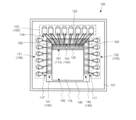
- FIG. 1 is sectional drawing which shows the whole structure of an acceleration sensor
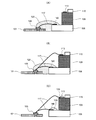
- FIG. 2 is a top view which shows the whole structure of an acceleration sensor is there. It is sectional drawing for demonstrating a part of manufacturing method of the acceleration sensor of FIG. 1, (A) is sectional drawing for demonstrating the process of forming a sensor with a semiconductor substrate, (B) is a sensor of (A). Sectional drawing for demonstrating the process of joining a sensor upper cap and a sensor lower cap to FIG. 2, (C) is sectional drawing for demonstrating the formation process of a board
- FIG. 1 It is sectional drawing for demonstrating a part of manufacturing method of the acceleration sensor of FIG. 1, (A) demonstrates the joining process of the sensor of FIG. 2 (B), the connection process of a bonding wire, and the application
- FIG. 3 It is a top view of the acceleration sensor for demonstrating a part of application
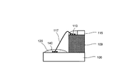
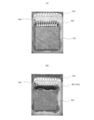
- (A) is the process which covers the electrode pad of a control IC, and the electrode pad of a sensor with potting resin It is a fragmentary sectional view of the acceleration sensor for explaining. It is a top view for demonstrating the specific example of the sensor which concerns on 1st Embodiment, (A) is a top view for demonstrating the structural example of a sensor, (B) is the some of the sensor of (A). It is a top view which shows the state which sealed the electrode pad with potting resin.
- FIG. 15 is a cross-sectional view taken along the line AA of FIG.
- FIG. 14 for explaining an example of the method for manufacturing the electrode pad and the separation portion according to the second embodiment
- FIG. 14 is a cross-sectional view taken along line AA in FIG. 14
- FIG. 14B is a cross-sectional view taken along line AA in FIG. 14 for explaining a potting resin coating process
- FIG. 15A is a cross-sectional view taken along the line AA of FIG. 14 for explaining another example of the method for manufacturing the electrode pad and the separation portion according to the second embodiment
- FIG. FIG. 14 is a cross-sectional view taken along line AA in FIG. 14 for explanation
- FIG. 14B is a cross-sectional view taken along line AA in FIG. 14 for explaining a potting resin coating process.
- It is a top view which shows the structure of the sensor for demonstrating the specific example of the resin potting of the acceleration sensor which concerns on 2nd Embodiment.
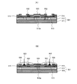
- FIG. 1 is a cross-sectional view showing the overall configuration of the acceleration sensor 100 according to the first embodiment.
- the control IC is packaged together with the acceleration sensor
- the present invention is not limited to this, and only the sensor may be packaged.
- FIG. 1A is a cross-sectional view showing the overall configuration of the acceleration sensor 100
- FIG. 1B is a plan view showing the overall configuration of the acceleration sensor 100
- the acceleration sensor 100 includes a substrate 101, a through electrode 105, a control IC 106, a sensor lower cap 107, a sensor 109, a sensor upper cap 115, a package cap 116, a bonding wire 118, and the like
- FIG. 1B is a plan view of the acceleration sensor 100 as viewed from the upper surface side, except for the package cap 116 of the acceleration sensor 100 shown in FIG. In FIG.
- electrode groups 131 to 133 each having a plurality of through electrodes 105 are arranged in the left and right regions and the upper region of the substrate 101 in the drawing.
- Electrode groups 141 to 143 each having a plurality of electrode pads 140 are arranged in the left and right regions and the upper region of the control IC 106 in the drawing.
- An electrode group 151 having a plurality of electrode pads 113 is arranged in the upper region of the sensor 109 in the drawing.
- the substrate 101 is a printed wiring board having a three-layer structure including a wiring layer 102, an insulating layer 103, and a wiring layer 104.
- the insulating layer 103 includes an insulating material
- the wiring layers 102 and 104 include a conductive material.
- the conductive substance is a metal or the like, and for example, copper, silver, gold, nickel, palladium, or the like can be used.
- An insulating resin is used as the insulating material.
- epoxy resin, polyimide resin, phenol resin, silicon resin, polyester, polyacetal, polycarbonate, or the like can be used.
- the resin may be used alone or in combination of two or more resins.
- an inorganic filler such as glass, talc, or silica may be used in combination with the resin.
- the substrate 101 includes three layers.
- the present invention is not limited to this, and the number of layers of the substrate 101 may be three or less, or three or more. May be.
- the through electrode 105 is formed through the substrate 101 and is electrically connected to the wiring layers 102 and 104.
- a plurality of electrode pads 140 (metal electrodes) for connecting to the through electrodes 105 are formed at predetermined positions on the upper surface of the substrate 101 shown in the drawing.
- the sensor 109 includes a fixed portion 110, a flexible portion 111 connected to the fixed portion 110, a weight portion 112 connected to the flexible portion 111, and a displacement of the flexible portion 111 disposed in the flexible portion 111. It includes a plurality of piezoresistive elements (not shown) that detect in the three-axis directions of XYZ, and electrode pads 113 (metal electrodes).
- the weight portion 112 When acceleration is applied to the sensor 109, the weight portion 112 is displaced, and the flexible portion 111 is bent along with the displacement.
- a force is applied to the piezoresistive element arranged in the flexible part 111, and the resistance value of the piezoresistive element changes.
- the change in the resistance value is detected, and the magnitude and direction of the acceleration applied to the sensor 109 are detected.
- a signal from the sensor 109 is transmitted from the electrode pad 113 to the control IC 106 through the bonding wire 118, the through electrode 105, and the like.
- a signal from the control IC 106 is transmitted to the outside of the substrate 101 through the bonding wire 117 and the through electrode 105.
- a sensor lower cap 107 is joined to a lower portion in the drawing.
- the sensor upper cap 115 is formed so as to cover the upper part of the flexible part 111 and the weight part 112 of the sensor 109, and is joined to the upper surface of the fixed part 110 of the sensor 109 by a resin 114 or the like.
- the sensor upper cap 115 limits excessive displacement of the weight portion 112 and the flexible portion 111 in the upward direction, and prevents breakage.
- the sensor upper cap 115 may be omitted.
- the package cap 116 may play the same role as the sensor upper cap 115.
- a convex stopper may be formed on the portion of the package cap 116 that faces the upper surface of the sensor 109.
- the package cap 116 includes an organic material, and an insulating resin such as an epoxy resin, an acrylic resin, or a polyimide resin is used.
- the package cap 116 is bonded to the upper surface of the substrate 101 of the substrate 101 by an adhesive (not shown).
- the sensor 109 is not sealed with resin, and the inside of the package cap 116 is hollow. That is, the acceleration sensor 100 uses a hollow package.
- 120 is a potting resin.
- the potting resin 120 is applied on the electrode pad 113 of the sensor 109 and the electrode pad 140 of the control IC 106 to cover the electrode pad 113 and the electrode pad 140.
- the electrode pad 113 and the through electrode 105 of the sensor 109 are connected to the electrode pad 140 and the through electrode 105 of the control IC 106 by the bonding wire 118, respectively, and the through electrode 105 and the electrode pad 140 of the control IC 106 are connected by the bonding wire 117. It is applied after being connected. Since the potting resin 120 is applied onto the electrode pad 113 of the sensor 109 and the electrode pad 140 of the control IC 106, a part of the bonding wires 117 and 118 are exposed.
- the potting resin 120 has an insulating property such as a silicon resin, an acrylic resin, an epoxy resin, a polyimide resin, and a urethane resin, and a resin material that can be applied on the electrode pad pad after wire bonding can be selected. desirable. In addition, it is desirable to select a material having a low water absorption (water absorption) as the potting resin 120. In the first embodiment, the water absorption rate is used as an index for evaluating the moisture resistance of the potting resin 120. This water absorption is determined from the ratio of the resin to the mass of the resin, for example, by storing the resin in a thermostatic chamber at a temperature of 85 ° C.
- the potting resin 120 is applied in order to prevent the electrode pad from being corroded from the humid outside air. Therefore, a potting resin having a low water absorption rate relative to an electrode pad using a metal material that is easily oxidized by moisture in the atmosphere such as Al or aluminum alloy, for example, Al-Si, Al-Si-Cu, Al-Nd, etc. It is effective to apply 120. Further, by limiting the application area of the potting resin 120 to the electrode pad after wire bonding, the sensor 109 is prevented from warping due to the application of the potting resin 120, and the potting resin 120 gives the sensor 109. By reducing the influence of stress, it is possible to prevent the offset voltage and sensitivity characteristics of the acceleration sensor 100 from being adversely affected. For this reason, as a material used as the potting resin 120, it is desirable to select a resin material having a low flexural modulus among the silicon resin, acrylic resin, epoxy resin, polyimide resin, urethane resin, and the like.
- FIGS. 2 and 3 show each manufacturing process based on the cross-sectional view of the acceleration sensor 100 shown in FIG.
- the sensor 109 having the fixed part 110, the flexible part 111, and the weight part 112 is formed by etching the fixed part 110, the flexible part 111, and the weight part 112.
- etching method a DRIE (Deep Reactive Ion Etching) method can be used.
- the substrate 101 including the wiring layer 102, the insulating layer 103, and the wiring layer 104 is manufactured, and the through electrode 105 is formed in a portion shown in the drawing.
- the through electrode 105 is formed by forming a recess (not shown) penetrating the substrate 101 and filling the recess with a conductive material.
- a control IC 106 is bonded to the upper surface of the substrate 101 on which the through electrode 105 is formed by a die attach (die bonding) 108 or the like.
- the sensor 109 shown in FIG. 2B is bonded to the upper surface of the control IC 106 shown in FIG. 2C by die attach (die bonding) 108 or the like.
- the electrode pad 113 of the sensor 109 and the through electrode 105 of the substrate 101, one electrode pad 140 (on the right side in the drawing) formed on the upper surface of the control IC 106 and the through electrode 105 of the substrate 101 are bonded to the bonding wire 118.
- the other electrode pad 140 (left side in the figure) formed on the upper surface of the control IC 106 and the through electrode 105 of the substrate 101 are connected by a bonding wire 117.
- FIGS. 4 to 7 are plan views of the acceleration sensor 100 in a state where the sensor upper cap 115 is joined except for the package cap 116 of the acceleration sensor 100 shown in FIG.
- the package cap 116 is bonded to the upper surface of the substrate 101 with an adhesive (not shown), the sensor 109, the plurality of electrode pads 113 of the sensor 109, the plurality of electrode pads 140 of the control IC 106, and the substrate 101.
- the plurality of through electrodes 105 are covered and sealed.
- the sensor 109 and the control IC 106 are not sealed with resin, and the inside of the package cap 116 is hollow.
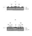
- FIG. 8A is a partial cross-sectional view showing an example of a state in which the through electrode of the substrate, the bonding wire, and the electrode pad of the control IC are sealed with potting resin
- FIG. 8C is a partial cross-sectional view showing another example of the state in which the wire and the electrode pad of the control IC are sealed with potting resin
- FIG. 8C shows another state in which the potting resin is applied to each electrode pad of the through electrode and sensor. It is a fragmentary sectional view showing an example.
- FIG. 8A is a partial cross-sectional view showing an example of a state in which the through electrode of the substrate, the bonding wire, and the electrode pad of the control IC are sealed with potting resin
- FIG. 8C is a partial cross-sectional view showing another example of the state in which the wire and the electrode pad of the control IC are sealed with potting resin
- FIG. 8C shows another state in which the potting resin is applied to each electrode pad of the through electrode and sensor. It is a fragment
- FIG. 9 is a partial cross-sectional view showing an example of a state in which the electrode pad of the control IC and the electrode pad of the sensor are sealed with potting resin.
- 8A, 8B, and 8C and FIG. 9 illustrate a partial configuration of each part of the through electrode 105 of the substrate 101, the electrode pad 140 of the control IC 106, and the electrode pad 113 of the sensor 109. It is sectional drawing simplified and shown. Further, in FIGS. 8A, 8B and 8C and FIG. 9, the same components as those of the acceleration sensor 100 shown in FIGS. 1 to 7 are denoted by the same reference numerals.
- the potting resin 120 is applied to the region including the through electrode 105, the electrode pad 140, and the bonding wire 117.
- the state which applied and sealed is shown. If the region including the through electrode 105, the electrode pad 140, and the bonding wire 117 is covered with the potting resin 120 in this way, the through electrode 105 of the substrate 101 and the sensor 109 are covered with the potting resin 120 as shown in FIG. It becomes difficult to connect to the electrode pad 113 by the bonding wire 117.
- the electrode pad 140 of the control IC 106 and the electrode pad 113 of the sensor 109 are connected by the bonding wire 117, and then potted on the electrode pad 140 and the electrode pad 113, respectively. Resin 120 may be applied and sealed.
- the potting resin 120 shown in FIG. 9 is applied only on the electrode pad 140 and the electrode pad 113, the electrode pad 140 and the electrode pad 113 can be prevented from being oxidized, and the potting resin 120 can be applied to the sensor 109. It is also possible to prevent warping.
- the potting resin 120 is applied and covered on the electrode pads 113 and 140, respectively. Is desirable.
- the connection procedure by the bonding wires 117 and 118 between the through electrode 105 of the substrate 101, the electrode pad 140 on the control IC 106, and the electrode pad 113 on the sensor 109 shown in FIGS. 4 to 7, and the through electrode 105 and the electrode pad The procedure for applying the potting resin 120 to 113 and 140 is the same. Therefore, in the acceleration sensor 100 shown in FIG.
- the potting resin 120 is applied to the electrode groups 141 to 143 each having the plurality of electrode pads 140 of the control IC 106 and the electrode group 151 having the plurality of electrode pads 113 of the sensor 109.
- the electrode pad 140 and the electrode pad 113 By coating and covering, it is possible to prevent the electrode pad 140 and the electrode pad 113 from being oxidized, and to prevent the sensor 109 from being warped by the potting resin 120.
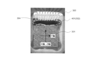
- FIG. 10A is a plan view of the sensor before applying the potting resin as seen from above
- FIG. 10B is a plan view of the sensor after applying the potting resin as seen from above.
- reference numeral 301 denotes a sensor
- 302 denotes an electrode pad formed on the sensor 301
- 303 denotes an electrode pad formed on the substrate
- 304 denotes a bonding wire.
- FIG. 10A the electrode pad 302 of the sensor 301 and the electrode pad 303 of the substrate were connected by a bonding wire 304.
- a potting resin 401 was applied on the electrode pad 302 of the sensor 301.
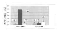
- FIG. 11 is a plan view of an acceleration sensor showing an acceleration detection direction as a measurement target of offset voltage deviation.
- FIG. 12 is a graph showing the measurement result of the offset voltage for each acceleration detection direction of the acceleration sensor shown in FIG. 11 after applying an epoxy resin or a silicon resin.
- the plurality of piezoresistive elements that detect the displacement of the flexible portion 111 shown in FIG. 1 in the XYZ 3-axis directions are the plurality of piezoresistors that detect the acceleration in the Y-axis direction in the Y-axis direction in the drawing. It is assumed that elements are arranged and a plurality of piezoresistive elements for detecting acceleration in the X and Z axis directions are arranged in the X and Z axis directions in the drawing.
- the epoxy resin is model number: ES-347-1 (Sanyu Rec Co., Ltd., flexural modulus: 18 [GPa] (the flexural modulus is measured according to JIS K9611)), and the silicone resin is model number: TSJ3155B. (Momentive Performance Materials Japan GK, durometer hardness: 70-82) was used.
- the deviation of the offset voltage generated in the sensor 301 when the epoxy resin is applied is caused by the magnitude of stress applied to the sensor 301 by the epoxy resin after the epoxy resin is applied. That is, the bending elastic modulus of the epoxy resin is related to the degree of warpage generated in the sensor 301. For this reason, the bending elastic modulus of the epoxy resin is changed, the offset voltage in the XYZ 3-axis direction of the sensor 301 is measured, and the usable range of the bending elastic modulus of the epoxy resin in which the offset voltage deviation is reduced is verified. Is shown in FIG.
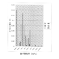
- FIG. 13 shows that the flexural modulus is 26 [GPa], 24 [GPa], 9 [GPa], 7 [GPa], 6.5 [GPa], 5 [GPa], 3.5 [GPa], 0.9
- the offset voltage deviation in the XYZ 3-axis direction of the sensor 301 is reduced when an epoxy resin having a flexural modulus of 5 [GPa] to 0.13 [GPa] is used. .
- the potting resin 401 when an epoxy resin is used as the potting resin 401, it is desirable to use a resin having a flexural modulus of 5 [GPa] or less. Further, since the measurement result of the offset voltage shown in FIG. 13 is a case where the entire sensor is molded using an epoxy resin, the epoxy resin is formed on the electrode pad 113 and the electrode pad 140 as shown in FIG. Even when the coating is applied, the influence of the stress applied to the sensor 109 by the epoxy resin is small, and there is no problem with the offset voltage deviation.
- the flexural modulus of the epoxy resin was measured based on JIS K6911 standard.
- the acceleration sensor after connecting the through electrode of the substrate, the electrode pad of the sensor, and the electrode pad of the control IC with the bonding wire, By coating and covering the minimum necessary area on the electrode pad of the control IC with a potting resin using a resin material that takes hygroscopicity and bending elastic modulus into account, corrosion of the electrode pad due to humid outside air can be prevented. In addition, it is possible to prevent warping of the sensor due to application of potting resin, and to reduce the influence of stress on the sensor due to potting resin. As a result, the influence on the sensor characteristics of the acceleration sensor can be minimized, and the reliability of the acceleration sensor can be improved.
- the acceleration sensor has been described as an example.
- the present invention is not limited to this, and can be applied to other mechanical quantity sensors such as an angular velocity sensor.
- the case where a silicon resin or an epoxy resin is applied as the potting resin has been shown.
- the resin material is not particularly limited.
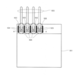
- FIG. 14 is a plan view showing a schematic configuration of the acceleration sensor 500.
- the entire configuration of the acceleration sensor 500 is the same as that of the acceleration sensor 100 shown in FIG.
- the sensor 501 of the acceleration sensor 500 has a plurality of electrode pads 502 formed in the upper region in the drawing.
- a bonding wire 503 is connected to each of the plurality of electrode pads 502.
- a plurality of separation portions 505 for separating the potting resin 506 applied on each electrode pad 502 is formed between the plurality of electrode pads 502.
- the acceleration sensor 500 according to the second embodiment of the present invention is characterized in that a plurality of separation portions 505 for separating the potting resin 506 are formed between the plurality of electrode pads 502.
- FIGS. 15A and 15B are partial cross-sectional views taken along the line AA in FIG. 14 and show an example of a method for manufacturing the separation portion 505 between the electrode pads 502.
- reference numeral 501 denotes a two-layer semiconductor substrate including a Si layer 511 and a SiO 2 layer 512.
- a plurality of electrodes 513 are formed by patterning or the like using Al—Nd or the like at positions corresponding to electrode pad formation positions on the upper surface of the semiconductor substrate 501.
- a dummy electrode 513a for forming a separation member is also formed between positions where electrode pads 502 described later are formed.
- the SiN layer 514 is formed on the upper surface of the semiconductor substrate 501 on which the plurality of electrodes 513 and the dummy electrodes 513a are formed, and the SiN layer 514 is etched using a mask (not shown) to form a plurality of electrode pads 502.
- a recess (not shown) is formed.
- a plurality of electrode pads 502 are formed by patterning the plurality of recesses using Al.
- a convex portion 505 is formed on the SiN layer 514 where the dummy electrode 513a is formed, and this convex portion 505 serves as a separation portion.
- FIG. 16A and 16B are partial cross-sectional views taken along the line AA in FIG. 14 and are diagrams illustrating an example of a method for manufacturing the separation portion 521 between the electrode pads 502.
- FIG. 16A and 16B the same components as those shown in FIGS. 15A and 15B are denoted by the same reference numerals.
- Electrode pad and separation part (see FIG. 16A)
- a plurality of electrodes 513 are formed by patterning or the like using Al—Nd or the like at positions corresponding to electrode pad formation positions on the upper surface of the semiconductor substrate 501.
- a SiN layer 514 is formed on the upper surface of the semiconductor substrate 501 on which the plurality of electrodes 513 are formed, and a plurality of recesses (see FIG. 5) are formed at positions where the electrode pads 502 are formed by etching the SiN layer 514 with a mask (not shown). (Not shown).
- the plurality of recesses are patterned using Al to form a plurality of electrode pads 502, and at the same time, a dummy electrode 521 is formed on the upper surface of the SiN layer 514 between the plurality of electrode pads 502 using Al—Nd or the like. To do. This dummy electrode 521 becomes a separation part.
- FIG. 17 shows a specific example when a potting resin is applied onto the electrode pad of the sensor.
- reference numeral 601 denotes a sensor
- 602 denotes a plurality of Al electrode pads formed on the sensor 601
- 603 denotes a plurality of Al electrode pads formed on the control IC
- 604 denotes a plurality of bonding wires.
- 605 is a plurality of separation parts for separating the potting resin
- 606 is the potting resin.
- each electrode pad 602 of the sensor 601 and each electrode pad 603 of the control IC are connected by a plurality of bonding wires 604.
- a potting resin 606 was applied on each electrode pad 602 of the sensor 601. It was confirmed that the formation of the separation portion 605 between the plurality of electrode pads 602 can prevent the potting resin 606 from spreading to the adjacent electrode pads 602.
- the material of the potting resin applied in FIG. 15B, FIG. 16B, and FIG. 17 is silicon that satisfies the conditions of the hygroscopicity and the flexural modulus as described in the first embodiment. It is desirable to use an epoxy resin or an epoxy resin. However, any resin material that satisfies the above conditions of hygroscopicity and flexural modulus may be used, and the resin material is not particularly limited.
- FIG. 15 shows the case where the convex portion 505 serving as the separation portion is formed by the dummy electrode 513a
- FIG. 16 shows the case where the separation portion is formed by the dummy electrode 521. However, for example, it may be formed by dummy wiring. .
- the position where the separation portion is formed is not limited between the plurality of electrode pads 502 of the sensor 501, but is formed between the plurality of electrode pads of the control IC, and on the plurality of electrode pads of the control IC.
- the potting resin to be applied may be prevented from spreading to adjacent electrode pads.
- FIGS. 15 and 16 show the case where the separation portion is formed by the dummy electrode, the separation portion may be formed using an actual electrode or wiring.
- the separation portion that separates the potting resin is formed between the plurality of electrode pads of the sensor, thereby being applied on each electrode pad. Since the potting resin is prevented from spreading to adjacent electrode pads, it is possible to reduce the influence of the stress exerted on the sensor by the potting resin as compared with the case where the potting resin is applied to each electrode group having a plurality of electrode pads. Therefore, according to the acceleration sensor according to the second embodiment of the present invention, the electrode pad of the control IC and the electrode pad of the sensor are connected by the bonding wire, and then the sensor electrode pad and the sensor electrode pad are connected.
Abstract
L'invention porte sur un procédé de production d'un dispositif à capteur et sur un dispositif à capteur qui empêchent la corrosion d'électrodes métalliques d'un capteur due à de l'air ambiant humide, et qui empêchent un gauchissement du capteur dû à une résine d'encapsulation, ce qui réduit les effets sur les caractéristiques du capteur. Le procédé de production du dispositif à capteur comprend les opérations suivantes : une section fixe, une section mobile positionnée à l'intérieur de la section fixe, une section flexible raccordant la section fixe et la section mobile, et un capteur comprenant une pluralité d'électrodes métalliques, sont placés sur un substrat ; la pluralité d'électrodes métalliques du capteur et une pluralité de bornes du substrat sont électriquement connectées par des fils de connexion ; et des zones qui sont reliées aux fils de connexion d'une pluralité d'électrodes métalliques du capteur sont couvertes d'une résine de telle manière qu'une partie des fils de connexion entre la pluralité d'électrodes métalliques et la pluralité de bornes soit exposée.
Priority Applications (1)
| Application Number | Priority Date | Filing Date | Title |
|---|---|---|---|
| US13/729,311 US9209319B2 (en) | 2010-06-30 | 2012-12-28 | Sensor device manufacturing method and sensor device |
Applications Claiming Priority (2)
| Application Number | Priority Date | Filing Date | Title |
|---|---|---|---|
| JP2010150109A JP4968371B2 (ja) | 2010-06-30 | 2010-06-30 | センサデバイスの製造方法及びセンサデバイス |
| JP2010-150109 | 2010-06-30 |
Related Child Applications (2)
| Application Number | Title | Priority Date | Filing Date |
|---|---|---|---|
| US13/729,311 Continuation-In-Part US9209319B2 (en) | 2010-06-30 | 2012-12-28 | Sensor device manufacturing method and sensor device |
| US13/729,311 Continuation US9209319B2 (en) | 2010-06-30 | 2012-12-28 | Sensor device manufacturing method and sensor device |
Publications (1)
| Publication Number | Publication Date |
|---|---|
| WO2012002233A1 true WO2012002233A1 (fr) | 2012-01-05 |
Family
ID=45401953
Family Applications (1)
| Application Number | Title | Priority Date | Filing Date |
|---|---|---|---|
| PCT/JP2011/064313 WO2012002233A1 (fr) | 2010-06-30 | 2011-06-22 | Procédé de production de dispositif à capteur et dispositif à capteur |
Country Status (3)
| Country | Link |
|---|---|
| US (1) | US9209319B2 (fr) |
| JP (1) | JP4968371B2 (fr) |
| WO (1) | WO2012002233A1 (fr) |
Cited By (1)
| Publication number | Priority date | Publication date | Assignee | Title |
|---|---|---|---|---|
| CN110304604A (zh) * | 2019-06-18 | 2019-10-08 | 上海应用技术大学 | 一种mems传感器的封装方法 |
Families Citing this family (4)
| Publication number | Priority date | Publication date | Assignee | Title |
|---|---|---|---|---|
| JP4968371B2 (ja) * | 2010-06-30 | 2012-07-04 | 大日本印刷株式会社 | センサデバイスの製造方法及びセンサデバイス |
| TWI620707B (zh) * | 2014-03-11 | 2018-04-11 | 立錡科技股份有限公司 | 微機電模組以及其製造方法 |
| CN105514074B (zh) * | 2015-12-01 | 2018-07-03 | 上海伊诺尔信息技术有限公司 | 智能卡芯片封装结构及其制造方法 |
| JP6947367B2 (ja) * | 2016-12-20 | 2021-10-13 | ローム株式会社 | センサモジュールおよびその製造方法 |
Citations (3)
| Publication number | Priority date | Publication date | Assignee | Title |
|---|---|---|---|---|
| JPS62144368A (ja) * | 1985-12-19 | 1987-06-27 | Nec Corp | 半導体式圧力センサの保護膜 |
| JP2002090245A (ja) * | 2000-09-18 | 2002-03-27 | Denso Corp | センサ装置の製造方法 |
| JP2006145410A (ja) * | 2004-11-22 | 2006-06-08 | Matsushita Electric Works Ltd | 物理量センサの実装構造 |
Family Cites Families (20)
| Publication number | Priority date | Publication date | Assignee | Title |
|---|---|---|---|---|
| JPS56150830A (en) * | 1980-04-25 | 1981-11-21 | Hitachi Ltd | Semiconductor device |
| JPS60160627A (ja) | 1984-01-31 | 1985-08-22 | Fujitsu Ltd | 半導体集積回路装置 |
| JPH0748566B2 (ja) | 1989-09-27 | 1995-05-24 | 山武ハネウエル株式会社 | 加速度センサおよびその製造方法 |
| JP2719448B2 (ja) * | 1991-01-24 | 1998-02-25 | 三菱電機株式会社 | 半導体圧力検出装置 |
| JPH04258176A (ja) * | 1991-02-12 | 1992-09-14 | Mitsubishi Electric Corp | 半導体圧力センサ |
| US5333505A (en) * | 1992-01-13 | 1994-08-02 | Mitsubishi Denki Kabushiki Kaisha | Semiconductor pressure sensor for use at high temperature and pressure and method of manufacturing same |
| JPH06132545A (ja) * | 1992-10-19 | 1994-05-13 | Mitsubishi Electric Corp | 圧力検出装置 |
| US5434105A (en) * | 1994-03-04 | 1995-07-18 | National Semiconductor Corporation | Process for attaching a lead frame to a heat sink using a glob-top encapsulation |
| JP3433570B2 (ja) | 1995-05-26 | 2003-08-04 | 松下電工株式会社 | 半導体加速度センサ |
| JPH0961271A (ja) * | 1995-08-29 | 1997-03-07 | Mitsubishi Electric Corp | 半導体式センサ及びその製造方法 |
| US6401545B1 (en) * | 2000-01-25 | 2002-06-11 | Motorola, Inc. | Micro electro-mechanical system sensor with selective encapsulation and method therefor |
| JP2002098709A (ja) | 2000-09-26 | 2002-04-05 | Matsushita Electric Works Ltd | 半導体加速度センサ |
| US6769319B2 (en) * | 2001-07-09 | 2004-08-03 | Freescale Semiconductor, Inc. | Component having a filter |
| JP4516252B2 (ja) | 2001-11-22 | 2010-08-04 | パナソニック電工株式会社 | 半導体加速度センサの封止方法 |
| ITTO20030444A1 (it) * | 2003-06-13 | 2004-12-14 | Olivetti Jet Spa | Sensore di pressione a struttura integrata. |
| JP4277079B2 (ja) * | 2004-06-18 | 2009-06-10 | Okiセミコンダクタ株式会社 | 半導体加速度センサ装置及びその製造方法 |
| JP4524454B2 (ja) * | 2004-11-19 | 2010-08-18 | ルネサスエレクトロニクス株式会社 | 電子装置およびその製造方法 |
| KR100766498B1 (ko) * | 2006-10-16 | 2007-10-15 | 삼성전자주식회사 | 반도체 패키지 및 그 제조방법 |
| US7985628B2 (en) * | 2007-12-12 | 2011-07-26 | Stats Chippac Ltd. | Integrated circuit package system with interconnect lock |
| JP4968371B2 (ja) * | 2010-06-30 | 2012-07-04 | 大日本印刷株式会社 | センサデバイスの製造方法及びセンサデバイス |
-
2010
- 2010-06-30 JP JP2010150109A patent/JP4968371B2/ja active Active
-
2011
- 2011-06-22 WO PCT/JP2011/064313 patent/WO2012002233A1/fr active Application Filing
-
2012
- 2012-12-28 US US13/729,311 patent/US9209319B2/en active Active
Patent Citations (3)
| Publication number | Priority date | Publication date | Assignee | Title |
|---|---|---|---|---|
| JPS62144368A (ja) * | 1985-12-19 | 1987-06-27 | Nec Corp | 半導体式圧力センサの保護膜 |
| JP2002090245A (ja) * | 2000-09-18 | 2002-03-27 | Denso Corp | センサ装置の製造方法 |
| JP2006145410A (ja) * | 2004-11-22 | 2006-06-08 | Matsushita Electric Works Ltd | 物理量センサの実装構造 |
Cited By (1)
| Publication number | Priority date | Publication date | Assignee | Title |
|---|---|---|---|---|
| CN110304604A (zh) * | 2019-06-18 | 2019-10-08 | 上海应用技术大学 | 一种mems传感器的封装方法 |
Also Published As
| Publication number | Publication date |
|---|---|
| JP2012013528A (ja) | 2012-01-19 |
| US20130113055A1 (en) | 2013-05-09 |
| JP4968371B2 (ja) | 2012-07-04 |
| US9209319B2 (en) | 2015-12-08 |
Similar Documents
| Publication | Publication Date | Title |
|---|---|---|
| JP5486271B2 (ja) | 加速度センサ、及び加速度センサの製造方法 | |
| WO2010134181A1 (fr) | Structure présentant une puce montée sur celle-ci et module comportant la structure | |
| JP4692260B2 (ja) | 半導体力学量センサ装置およびその製造方法 | |
| JP4968371B2 (ja) | センサデバイスの製造方法及びセンサデバイス | |
| US8426930B2 (en) | Sensor module | |
| US9331010B2 (en) | System support for electronic components and method for production thereof | |
| EP3076146A1 (fr) | Capteur de pression | |
| JP5125978B2 (ja) | センサ装置 | |
| US7836764B2 (en) | Electrical device with covering | |
| US20160209344A1 (en) | Complex sensor and method of manufacturing the same | |
| JP2007240250A (ja) | 圧力センサ、圧力センサパッケージ、圧力センサモジュール、及び電子部品 | |
| KR20090124011A (ko) | 패키징 기판과 이를 포함하는 가스 센싱 장치 및 그 제조방법 | |
| JP5771915B2 (ja) | Memsデバイス及びその製造方法 | |
| JP5920501B2 (ja) | センサデバイスの製造方法及びセンサデバイス | |
| JP2005127750A (ja) | 半導体センサおよびその製造方法 | |
| JP6714439B2 (ja) | 歪検出器及びその製造方法 | |
| JP4949673B2 (ja) | 半導体加速度センサおよびその製造方法 | |
| JP5742170B2 (ja) | Memsデバイス、その製造方法、及びそれを有する半導体装置 | |
| JP2012181198A (ja) | センサデバイスの製造方法及びセンサデバイス | |
| JP4706634B2 (ja) | 半導体センサおよびその製造方法 | |
| JP2010078425A (ja) | 加速度センサ | |
| JP5328492B2 (ja) | 圧力センサモジュール及び圧力センサパッケージ、並びにこれらの製造方法 | |
| JP5328493B2 (ja) | 圧力センサモジュール及び圧力センサパッケージ、並びにこれらの製造方法 | |
| JP5328479B2 (ja) | 圧力センサモジュール及び圧力センサパッケージ、並びにこれらの製造方法 | |
| JP6507595B2 (ja) | 半導体センサ装置 |
Legal Events
| Date | Code | Title | Description |
|---|---|---|---|
| 121 | Ep: the epo has been informed by wipo that ep was designated in this application |
Ref document number: 11800698 Country of ref document: EP Kind code of ref document: A1 |
|
| NENP | Non-entry into the national phase |
Ref country code: DE |
|
| 122 | Ep: pct application non-entry in european phase |
Ref document number: 11800698 Country of ref document: EP Kind code of ref document: A1 |