WO2011140197A1 - Thick-film pastes containing lead- and tellurium-oxides, and their use in the manufacture of semiconductor devices - Google Patents
Thick-film pastes containing lead- and tellurium-oxides, and their use in the manufacture of semiconductor devices Download PDFInfo
- Publication number
- WO2011140197A1 WO2011140197A1 PCT/US2011/035154 US2011035154W WO2011140197A1 WO 2011140197 A1 WO2011140197 A1 WO 2011140197A1 US 2011035154 W US2011035154 W US 2011035154W WO 2011140197 A1 WO2011140197 A1 WO 2011140197A1
- Authority
- WO
- WIPO (PCT)
- Prior art keywords
- thick
- tellurium
- film paste
- lead
- oxide
- Prior art date
Links
- 239000004065 semiconductor Substances 0.000 title claims description 43
- 238000004519 manufacturing process Methods 0.000 title description 7
- 229910052751 metal Inorganic materials 0.000 claims abstract description 32
- 239000002184 metal Substances 0.000 claims abstract description 32
- 239000000203 mixture Substances 0.000 claims description 88
- 239000000758 substrate Substances 0.000 claims description 48
- 238000010304 firing Methods 0.000 claims description 30
- 238000000034 method Methods 0.000 claims description 29
- 229910052709 silver Inorganic materials 0.000 claims description 25
- 239000004332 silver Substances 0.000 claims description 25
- 239000007787 solid Substances 0.000 claims description 23
- 229910052714 tellurium Inorganic materials 0.000 claims description 16
- VYPSYNLAJGMNEJ-UHFFFAOYSA-N silicon dioxide Inorganic materials O=[Si]=O VYPSYNLAJGMNEJ-UHFFFAOYSA-N 0.000 claims description 15
- -1 M0O3 Inorganic materials 0.000 claims description 13
- PORWMNRCUJJQNO-UHFFFAOYSA-N tellurium atom Chemical compound [Te] PORWMNRCUJJQNO-UHFFFAOYSA-N 0.000 claims description 13
- GWEVSGVZZGPLCZ-UHFFFAOYSA-N titanium dioxide Inorganic materials O=[Ti]=O GWEVSGVZZGPLCZ-UHFFFAOYSA-N 0.000 claims description 11
- 229910052710 silicon Inorganic materials 0.000 claims description 9
- 239000002904 solvent Substances 0.000 claims description 9
- 239000000654 additive Substances 0.000 claims description 6
- 229920000642 polymer Polymers 0.000 claims description 5
- 239000004094 surface-active agent Substances 0.000 claims description 5
- MCMNRKCIXSYSNV-UHFFFAOYSA-N ZrO2 Inorganic materials O=[Zr]=O MCMNRKCIXSYSNV-UHFFFAOYSA-N 0.000 claims description 4
- 230000000996 additive effect Effects 0.000 claims description 4
- 239000012298 atmosphere Substances 0.000 claims description 4
- FPHIOHCCQGUGKU-UHFFFAOYSA-L difluorolead Chemical compound F[Pb]F FPHIOHCCQGUGKU-UHFFFAOYSA-L 0.000 claims description 4
- 229910052698 phosphorus Inorganic materials 0.000 claims description 4
- 229910052700 potassium Inorganic materials 0.000 claims description 3
- 229910052719 titanium Inorganic materials 0.000 claims description 3
- 229910052692 Dysprosium Inorganic materials 0.000 claims description 2
- 229910052693 Europium Inorganic materials 0.000 claims description 2
- 229910052688 Gadolinium Inorganic materials 0.000 claims description 2
- 229910052689 Holmium Inorganic materials 0.000 claims description 2
- 229910052779 Neodymium Inorganic materials 0.000 claims description 2
- 229910052777 Praseodymium Inorganic materials 0.000 claims description 2
- 229910052772 Samarium Inorganic materials 0.000 claims description 2
- 229910052769 Ytterbium Inorganic materials 0.000 claims description 2
- 229910052787 antimony Inorganic materials 0.000 claims description 2
- 229910052785 arsenic Inorganic materials 0.000 claims description 2
- QVGXLLKOCUKJST-UHFFFAOYSA-N atomic oxygen Chemical compound [O] QVGXLLKOCUKJST-UHFFFAOYSA-N 0.000 claims description 2
- 229910052793 cadmium Inorganic materials 0.000 claims description 2
- 229910052792 caesium Inorganic materials 0.000 claims description 2
- 229910052791 calcium Inorganic materials 0.000 claims description 2
- 229910052804 chromium Inorganic materials 0.000 claims description 2
- JKWMSGQKBLHBQQ-UHFFFAOYSA-N diboron trioxide Chemical compound O=BOB=O JKWMSGQKBLHBQQ-UHFFFAOYSA-N 0.000 claims description 2
- 229910052733 gallium Inorganic materials 0.000 claims description 2
- 229910052732 germanium Inorganic materials 0.000 claims description 2
- 229910052738 indium Inorganic materials 0.000 claims description 2
- 229910052746 lanthanum Inorganic materials 0.000 claims description 2
- 229910052744 lithium Inorganic materials 0.000 claims description 2
- 229910052749 magnesium Inorganic materials 0.000 claims description 2
- 229910052748 manganese Inorganic materials 0.000 claims description 2
- 229910052750 molybdenum Inorganic materials 0.000 claims description 2
- 229910052759 nickel Inorganic materials 0.000 claims description 2
- 229910052758 niobium Inorganic materials 0.000 claims description 2
- 229910052760 oxygen Inorganic materials 0.000 claims description 2
- 239000001301 oxygen Substances 0.000 claims description 2
- 229910052701 rubidium Inorganic materials 0.000 claims description 2
- 239000003381 stabilizer Substances 0.000 claims description 2
- 229910052712 strontium Inorganic materials 0.000 claims description 2
- 229910052715 tantalum Inorganic materials 0.000 claims description 2
- 239000002562 thickening agent Substances 0.000 claims description 2
- 229910052718 tin Inorganic materials 0.000 claims description 2
- 229910052721 tungsten Inorganic materials 0.000 claims description 2
- 229910052720 vanadium Inorganic materials 0.000 claims description 2
- 229910052727 yttrium Inorganic materials 0.000 claims description 2
- 229910052725 zinc Inorganic materials 0.000 claims description 2
- 229910052726 zirconium Inorganic materials 0.000 claims description 2
- 238000007639 printing Methods 0.000 abstract description 7
- 239000000843 powder Substances 0.000 description 33
- 239000010410 layer Substances 0.000 description 30
- BQCADISMDOOEFD-UHFFFAOYSA-N Silver Chemical compound [Ag] BQCADISMDOOEFD-UHFFFAOYSA-N 0.000 description 27
- 239000002609 medium Substances 0.000 description 23
- 229910052782 aluminium Inorganic materials 0.000 description 17
- XAGFODPZIPBFFR-UHFFFAOYSA-N aluminium Chemical compound [Al] XAGFODPZIPBFFR-UHFFFAOYSA-N 0.000 description 17
- 239000000306 component Substances 0.000 description 16
- YEXPOXQUZXUXJW-UHFFFAOYSA-N oxolead Chemical compound [Pb]=O YEXPOXQUZXUXJW-UHFFFAOYSA-N 0.000 description 16
- 238000002360 preparation method Methods 0.000 description 16
- 229910052581 Si3N4 Inorganic materials 0.000 description 15
- 239000011521 glass Substances 0.000 description 15
- HQVNEWCFYHHQES-UHFFFAOYSA-N silicon nitride Chemical compound N12[Si]34N5[Si]62N3[Si]51N64 HQVNEWCFYHHQES-UHFFFAOYSA-N 0.000 description 15
- 238000009792 diffusion process Methods 0.000 description 12
- 239000002245 particle Substances 0.000 description 12
- HTUMBQDCCIXGCV-UHFFFAOYSA-N lead oxide Chemical compound [O-2].[Pb+2] HTUMBQDCCIXGCV-UHFFFAOYSA-N 0.000 description 11
- 238000002156 mixing Methods 0.000 description 11
- 229910052814 silicon oxide Inorganic materials 0.000 description 10
- OGIDPMRJRNCKJF-UHFFFAOYSA-N titanium oxide Inorganic materials [Ti]=O OGIDPMRJRNCKJF-UHFFFAOYSA-N 0.000 description 8
- 235000012431 wafers Nutrition 0.000 description 8
- XUIMIQQOPSSXEZ-UHFFFAOYSA-N Silicon Chemical compound [Si] XUIMIQQOPSSXEZ-UHFFFAOYSA-N 0.000 description 7
- 239000006117 anti-reflective coating Substances 0.000 description 7
- 238000000576 coating method Methods 0.000 description 7
- 239000000463 material Substances 0.000 description 7
- 239000010703 silicon Substances 0.000 description 7
- 229910004205 SiNX Inorganic materials 0.000 description 6
- XLOMVQKBTHCTTD-UHFFFAOYSA-N Zinc monoxide Chemical compound [Zn]=O XLOMVQKBTHCTTD-UHFFFAOYSA-N 0.000 description 6
- 239000011248 coating agent Substances 0.000 description 6
- 239000004020 conductor Substances 0.000 description 6
- 238000007650 screen-printing Methods 0.000 description 6
- 239000006185 dispersion Substances 0.000 description 5
- 229910000464 lead oxide Inorganic materials 0.000 description 5
- 239000000155 melt Substances 0.000 description 5
- 238000000623 plasma-assisted chemical vapour deposition Methods 0.000 description 5
- 229910021420 polycrystalline silicon Inorganic materials 0.000 description 5
- OKTJSMMVPCPJKN-UHFFFAOYSA-N Carbon Chemical compound [C] OKTJSMMVPCPJKN-UHFFFAOYSA-N 0.000 description 4
- 238000001035 drying Methods 0.000 description 4
- 238000010438 heat treatment Methods 0.000 description 4
- 239000000976 ink Substances 0.000 description 4
- XHXFXVLFKHQFAL-UHFFFAOYSA-N phosphoryl trichloride Chemical compound ClP(Cl)(Cl)=O XHXFXVLFKHQFAL-UHFFFAOYSA-N 0.000 description 4
- BASFCYQUMIYNBI-UHFFFAOYSA-N platinum Chemical compound [Pt] BASFCYQUMIYNBI-UHFFFAOYSA-N 0.000 description 4
- 238000012545 processing Methods 0.000 description 4
- 238000004544 sputter deposition Methods 0.000 description 4
- QTBSBXVTEAMEQO-UHFFFAOYSA-N Acetic acid Chemical compound CC(O)=O QTBSBXVTEAMEQO-UHFFFAOYSA-N 0.000 description 3
- KFZMGEQAYNKOFK-UHFFFAOYSA-N Isopropanol Chemical compound CC(C)O KFZMGEQAYNKOFK-UHFFFAOYSA-N 0.000 description 3
- 150000001298 alcohols Chemical class 0.000 description 3
- 238000005229 chemical vapour deposition Methods 0.000 description 3
- 238000005530 etching Methods 0.000 description 3
- 150000002736 metal compounds Chemical class 0.000 description 3
- 239000010935 stainless steel Substances 0.000 description 3
- 229910001220 stainless steel Inorganic materials 0.000 description 3
- 238000010998 test method Methods 0.000 description 3
- 239000011787 zinc oxide Substances 0.000 description 3
- SVTBMSDMJJWYQN-UHFFFAOYSA-N 2-methylpentane-2,4-diol Chemical compound CC(O)CC(C)(C)O SVTBMSDMJJWYQN-UHFFFAOYSA-N 0.000 description 2
- RSWGJHLUYNHPMX-UHFFFAOYSA-N Abietic-Saeure Natural products C12CCC(C(C)C)=CC2=CCC2C1(C)CCCC2(C)C(O)=O RSWGJHLUYNHPMX-UHFFFAOYSA-N 0.000 description 2
- RYGMFSIKBFXOCR-UHFFFAOYSA-N Copper Chemical compound [Cu] RYGMFSIKBFXOCR-UHFFFAOYSA-N 0.000 description 2
- ZZSNKZQZMQGXPY-UHFFFAOYSA-N Ethyl cellulose Chemical compound CCOCC1OC(OC)C(OCC)C(OCC)C1OC1C(O)C(O)C(OC)C(CO)O1 ZZSNKZQZMQGXPY-UHFFFAOYSA-N 0.000 description 2
- 239000001856 Ethyl cellulose Substances 0.000 description 2
- KDLHZDBZIXYQEI-UHFFFAOYSA-N Palladium Chemical compound [Pd] KDLHZDBZIXYQEI-UHFFFAOYSA-N 0.000 description 2
- OAICVXFJPJFONN-UHFFFAOYSA-N Phosphorus Chemical compound [P] OAICVXFJPJFONN-UHFFFAOYSA-N 0.000 description 2
- 239000004698 Polyethylene Substances 0.000 description 2
- KHPCPRHQVVSZAH-HUOMCSJISA-N Rosin Natural products O(C/C=C/c1ccccc1)[C@H]1[C@H](O)[C@@H](O)[C@@H](O)[C@@H](CO)O1 KHPCPRHQVVSZAH-HUOMCSJISA-N 0.000 description 2
- HMDDXIMCDZRSNE-UHFFFAOYSA-N [C].[Si] Chemical compound [C].[Si] HMDDXIMCDZRSNE-UHFFFAOYSA-N 0.000 description 2
- 239000002253 acid Substances 0.000 description 2
- 229910052799 carbon Inorganic materials 0.000 description 2
- 229910002090 carbon oxide Inorganic materials 0.000 description 2
- 239000002800 charge carrier Substances 0.000 description 2
- 238000006243 chemical reaction Methods 0.000 description 2
- 239000000470 constituent Substances 0.000 description 2
- 229910052802 copper Inorganic materials 0.000 description 2
- 239000010949 copper Substances 0.000 description 2
- GHVNFZFCNZKVNT-UHFFFAOYSA-N decanoic acid Chemical compound CCCCCCCCCC(O)=O GHVNFZFCNZKVNT-UHFFFAOYSA-N 0.000 description 2
- 230000001419 dependent effect Effects 0.000 description 2
- DOIRQSBPFJWKBE-UHFFFAOYSA-N dibutyl phthalate Chemical compound CCCCOC(=O)C1=CC=CC=C1C(=O)OCCCC DOIRQSBPFJWKBE-UHFFFAOYSA-N 0.000 description 2
- FSCIDASGDAWVED-UHFFFAOYSA-N dimethyl hexanedioate;dimethyl pentanedioate Chemical compound COC(=O)CCCC(=O)OC.COC(=O)CCCCC(=O)OC FSCIDASGDAWVED-UHFFFAOYSA-N 0.000 description 2
- 238000009826 distribution Methods 0.000 description 2
- POULHZVOKOAJMA-UHFFFAOYSA-N dodecanoic acid Chemical compound CCCCCCCCCCCC(O)=O POULHZVOKOAJMA-UHFFFAOYSA-N 0.000 description 2
- 239000000839 emulsion Substances 0.000 description 2
- 229920001249 ethyl cellulose Polymers 0.000 description 2
- 235000019325 ethyl cellulose Nutrition 0.000 description 2
- IPCSVZSSVZVIGE-UHFFFAOYSA-N hexadecanoic acid Chemical compound CCCCCCCCCCCCCCCC(O)=O IPCSVZSSVZVIGE-UHFFFAOYSA-N 0.000 description 2
- 239000011229 interlayer Substances 0.000 description 2
- 239000007788 liquid Substances 0.000 description 2
- 229910021421 monocrystalline silicon Inorganic materials 0.000 description 2
- QIQXTHQIDYTFRH-UHFFFAOYSA-N octadecanoic acid Chemical compound CCCCCCCCCCCCCCCCCC(O)=O QIQXTHQIDYTFRH-UHFFFAOYSA-N 0.000 description 2
- TWNQGVIAIRXVLR-UHFFFAOYSA-N oxo(oxoalumanyloxy)alumane Chemical compound O=[Al]O[Al]=O TWNQGVIAIRXVLR-UHFFFAOYSA-N 0.000 description 2
- NBIIXXVUZAFLBC-UHFFFAOYSA-K phosphate Chemical compound [O-]P([O-])([O-])=O NBIIXXVUZAFLBC-UHFFFAOYSA-K 0.000 description 2
- 239000011574 phosphorus Substances 0.000 description 2
- 229910052697 platinum Inorganic materials 0.000 description 2
- 229920000573 polyethylene Polymers 0.000 description 2
- 229920001223 polyethylene glycol Polymers 0.000 description 2
- 239000011347 resin Substances 0.000 description 2
- 229920005989 resin Polymers 0.000 description 2
- 150000003378 silver Chemical class 0.000 description 2
- NDVLTYZPCACLMA-UHFFFAOYSA-N silver oxide Chemical compound [O-2].[Ag+].[Ag+] NDVLTYZPCACLMA-UHFFFAOYSA-N 0.000 description 2
- 238000002230 thermal chemical vapour deposition Methods 0.000 description 2
- 239000010936 titanium Substances 0.000 description 2
- KHPCPRHQVVSZAH-UHFFFAOYSA-N trans-cinnamyl beta-D-glucopyranoside Natural products OC1C(O)C(O)C(CO)OC1OCC=CC1=CC=CC=C1 KHPCPRHQVVSZAH-UHFFFAOYSA-N 0.000 description 2
- WRIDQFICGBMAFQ-UHFFFAOYSA-N (E)-8-Octadecenoic acid Natural products CCCCCCCCCC=CCCCCCCC(O)=O WRIDQFICGBMAFQ-UHFFFAOYSA-N 0.000 description 1
- WUOACPNHFRMFPN-SECBINFHSA-N (S)-(-)-alpha-terpineol Chemical compound CC1=CC[C@@H](C(C)(C)O)CC1 WUOACPNHFRMFPN-SECBINFHSA-N 0.000 description 1
- RUJPNZNXGCHGID-UHFFFAOYSA-N (Z)-beta-Terpineol Natural products CC(=C)C1CCC(C)(O)CC1 RUJPNZNXGCHGID-UHFFFAOYSA-N 0.000 description 1
- PAAZPARNPHGIKF-UHFFFAOYSA-N 1,2-dibromoethane Chemical compound BrCCBr PAAZPARNPHGIKF-UHFFFAOYSA-N 0.000 description 1
- HMUNWXXNJPVALC-UHFFFAOYSA-N 1-[4-[2-(2,3-dihydro-1H-inden-2-ylamino)pyrimidin-5-yl]piperazin-1-yl]-2-(2,4,6,7-tetrahydrotriazolo[4,5-c]pyridin-5-yl)ethanone Chemical compound C1C(CC2=CC=CC=C12)NC1=NC=C(C=N1)N1CCN(CC1)C(CN1CC2=C(CC1)NN=N2)=O HMUNWXXNJPVALC-UHFFFAOYSA-N 0.000 description 1
- ZXUOFCUEFQCKKH-UHFFFAOYSA-N 12-methyltridecan-1-ol Chemical compound CC(C)CCCCCCCCCCCO ZXUOFCUEFQCKKH-UHFFFAOYSA-N 0.000 description 1
- OAYXUHPQHDHDDZ-UHFFFAOYSA-N 2-(2-butoxyethoxy)ethanol Chemical compound CCCCOCCOCCO OAYXUHPQHDHDDZ-UHFFFAOYSA-N 0.000 description 1
- VXQBJTKSVGFQOL-UHFFFAOYSA-N 2-(2-butoxyethoxy)ethyl acetate Chemical compound CCCCOCCOCCOC(C)=O VXQBJTKSVGFQOL-UHFFFAOYSA-N 0.000 description 1
- POAOYUHQDCAZBD-UHFFFAOYSA-N 2-butoxyethanol Chemical compound CCCCOCCO POAOYUHQDCAZBD-UHFFFAOYSA-N 0.000 description 1
- LQJBNNIYVWPHFW-UHFFFAOYSA-N 20:1omega9c fatty acid Natural products CCCCCCCCCCC=CCCCCCCCC(O)=O LQJBNNIYVWPHFW-UHFFFAOYSA-N 0.000 description 1
- KEOUIRVJRXECRC-UHFFFAOYSA-N 6-[2-(2-butoxyethoxy)ethoxy]-6-oxohexanoic acid Chemical compound CCCCOCCOCCOC(=O)CCCCC(O)=O KEOUIRVJRXECRC-UHFFFAOYSA-N 0.000 description 1
- QSBYPNXLFMSGKH-UHFFFAOYSA-N 9-Heptadecensaeure Natural products CCCCCCCC=CCCCCCCCC(O)=O QSBYPNXLFMSGKH-UHFFFAOYSA-N 0.000 description 1
- 229910001316 Ag alloy Inorganic materials 0.000 description 1
- QGZKDVFQNNGYKY-UHFFFAOYSA-O Ammonium Chemical compound [NH4+] QGZKDVFQNNGYKY-UHFFFAOYSA-O 0.000 description 1
- 239000005632 Capric acid (CAS 334-48-5) Substances 0.000 description 1
- MUXOBHXGJLMRAB-UHFFFAOYSA-N Dimethyl succinate Chemical compound COC(=O)CCC(=O)OC MUXOBHXGJLMRAB-UHFFFAOYSA-N 0.000 description 1
- 239000004593 Epoxy Substances 0.000 description 1
- 229920000896 Ethulose Polymers 0.000 description 1
- 239000001859 Ethyl hydroxyethyl cellulose Substances 0.000 description 1
- UFHFLCQGNIYNRP-UHFFFAOYSA-N Hydrogen Chemical compound [H][H] UFHFLCQGNIYNRP-UHFFFAOYSA-N 0.000 description 1
- DGAQECJNVWCQMB-PUAWFVPOSA-M Ilexoside XXIX Chemical compound C[C@@H]1CC[C@@]2(CC[C@@]3(C(=CC[C@H]4[C@]3(CC[C@@H]5[C@@]4(CC[C@@H](C5(C)C)OS(=O)(=O)[O-])C)C)[C@@H]2[C@]1(C)O)C)C(=O)O[C@H]6[C@@H]([C@H]([C@@H]([C@H](O6)CO)O)O)O.[Na+] DGAQECJNVWCQMB-PUAWFVPOSA-M 0.000 description 1
- 239000005639 Lauric acid Substances 0.000 description 1
- OYHQOLUKZRVURQ-HZJYTTRNSA-N Linoleic acid Chemical compound CCCCC\C=C/C\C=C/CCCCCCCC(O)=O OYHQOLUKZRVURQ-HZJYTTRNSA-N 0.000 description 1
- 229910007052 Li—Ti—O Inorganic materials 0.000 description 1
- 239000005642 Oleic acid Substances 0.000 description 1
- ZQPPMHVWECSIRJ-UHFFFAOYSA-N Oleic acid Natural products CCCCCCCCC=CCCCCCCCC(O)=O ZQPPMHVWECSIRJ-UHFFFAOYSA-N 0.000 description 1
- 229910019142 PO4 Inorganic materials 0.000 description 1
- 235000021314 Palmitic acid Nutrition 0.000 description 1
- 229920003171 Poly (ethylene oxide) Polymers 0.000 description 1
- 239000002202 Polyethylene glycol Substances 0.000 description 1
- ZLMJMSJWJFRBEC-UHFFFAOYSA-N Potassium Chemical compound [K] ZLMJMSJWJFRBEC-UHFFFAOYSA-N 0.000 description 1
- 229910001260 Pt alloy Inorganic materials 0.000 description 1
- 235000021355 Stearic acid Nutrition 0.000 description 1
- RTAQQCXQSZGOHL-UHFFFAOYSA-N Titanium Chemical compound [Ti] RTAQQCXQSZGOHL-UHFFFAOYSA-N 0.000 description 1
- AEDKJFTVSXSKIZ-UHFFFAOYSA-N [Bi].[Te]=O Chemical compound [Bi].[Te]=O AEDKJFTVSXSKIZ-UHFFFAOYSA-N 0.000 description 1
- 229910045601 alloy Inorganic materials 0.000 description 1
- 239000000956 alloy Substances 0.000 description 1
- OVKDFILSBMEKLT-UHFFFAOYSA-N alpha-Terpineol Natural products CC(=C)C1(O)CCC(C)=CC1 OVKDFILSBMEKLT-UHFFFAOYSA-N 0.000 description 1
- 238000000498 ball milling Methods 0.000 description 1
- QRUDEWIWKLJBPS-UHFFFAOYSA-N benzotriazole Chemical compound C1=CC=C2N[N][N]C2=C1 QRUDEWIWKLJBPS-UHFFFAOYSA-N 0.000 description 1
- 239000012964 benzotriazole Substances 0.000 description 1
- 239000011230 binding agent Substances 0.000 description 1
- 230000015572 biosynthetic process Effects 0.000 description 1
- HUTDDBSSHVOYJR-UHFFFAOYSA-H bis[(2-oxo-1,3,2$l^{5},4$l^{2}-dioxaphosphaplumbetan-2-yl)oxy]lead Chemical compound [Pb+2].[Pb+2].[Pb+2].[O-]P([O-])([O-])=O.[O-]P([O-])([O-])=O HUTDDBSSHVOYJR-UHFFFAOYSA-H 0.000 description 1
- 229910000416 bismuth oxide Inorganic materials 0.000 description 1
- 238000009835 boiling Methods 0.000 description 1
- 239000003153 chemical reaction reagent Substances 0.000 description 1
- 230000000052 comparative effect Effects 0.000 description 1
- 229910021419 crystalline silicon Inorganic materials 0.000 description 1
- 238000000151 deposition Methods 0.000 description 1
- 230000008021 deposition Effects 0.000 description 1
- 238000010586 diagram Methods 0.000 description 1
- 229910003460 diamond Inorganic materials 0.000 description 1
- 239000010432 diamond Substances 0.000 description 1
- TYIXMATWDRGMPF-UHFFFAOYSA-N dibismuth;oxygen(2-) Chemical compound [O-2].[O-2].[O-2].[Bi+3].[Bi+3] TYIXMATWDRGMPF-UHFFFAOYSA-N 0.000 description 1
- 229960002380 dibutyl phthalate Drugs 0.000 description 1
- BNMYXGKEMMVHOX-UHFFFAOYSA-N dimethyl butanedioate;dimethyl pentanedioate Chemical compound COC(=O)CCC(=O)OC.COC(=O)CCCC(=O)OC BNMYXGKEMMVHOX-UHFFFAOYSA-N 0.000 description 1
- XTDYIOOONNVFMA-UHFFFAOYSA-N dimethyl pentanedioate Chemical compound COC(=O)CCCC(=O)OC XTDYIOOONNVFMA-UHFFFAOYSA-N 0.000 description 1
- 239000002019 doping agent Substances 0.000 description 1
- 230000000694 effects Effects 0.000 description 1
- 230000005684 electric field Effects 0.000 description 1
- 150000002148 esters Chemical class 0.000 description 1
- 235000019326 ethyl hydroxyethyl cellulose Nutrition 0.000 description 1
- 238000011156 evaluation Methods 0.000 description 1
- 238000002474 experimental method Methods 0.000 description 1
- 238000001125 extrusion Methods 0.000 description 1
- 230000004907 flux Effects 0.000 description 1
- 239000002803 fossil fuel Substances 0.000 description 1
- 230000004927 fusion Effects 0.000 description 1
- 238000000227 grinding Methods 0.000 description 1
- 229940051250 hexylene glycol Drugs 0.000 description 1
- 229910052739 hydrogen Inorganic materials 0.000 description 1
- 239000001257 hydrogen Substances 0.000 description 1
- 229910010272 inorganic material Inorganic materials 0.000 description 1
- 239000011147 inorganic material Substances 0.000 description 1
- 239000012212 insulator Substances 0.000 description 1
- 230000001788 irregular Effects 0.000 description 1
- QXJSBBXBKPUZAA-UHFFFAOYSA-N isooleic acid Natural products CCCCCCCC=CCCCCCCCCC(O)=O QXJSBBXBKPUZAA-UHFFFAOYSA-N 0.000 description 1
- 239000003350 kerosene Substances 0.000 description 1
- 150000002611 lead compounds Chemical class 0.000 description 1
- 229960004232 linoleic acid Drugs 0.000 description 1
- 239000011344 liquid material Substances 0.000 description 1
- XGZVUEUWXADBQD-UHFFFAOYSA-L lithium carbonate Chemical compound [Li+].[Li+].[O-]C([O-])=O XGZVUEUWXADBQD-UHFFFAOYSA-L 0.000 description 1
- 229910052808 lithium carbonate Inorganic materials 0.000 description 1
- 229910001947 lithium oxide Inorganic materials 0.000 description 1
- 229910001386 lithium phosphate Inorganic materials 0.000 description 1
- 238000005259 measurement Methods 0.000 description 1
- 239000012533 medium component Substances 0.000 description 1
- 229910044991 metal oxide Inorganic materials 0.000 description 1
- 150000004706 metal oxides Chemical class 0.000 description 1
- 238000003801 milling Methods 0.000 description 1
- 238000012986 modification Methods 0.000 description 1
- 230000004048 modification Effects 0.000 description 1
- 239000004570 mortar (masonry) Substances 0.000 description 1
- WQEPLUUGTLDZJY-UHFFFAOYSA-N n-Pentadecanoic acid Natural products CCCCCCCCCCCCCCC(O)=O WQEPLUUGTLDZJY-UHFFFAOYSA-N 0.000 description 1
- OQCDKBAXFALNLD-UHFFFAOYSA-N octadecanoic acid Natural products CCCCCCCC(C)CCCCCCCCC(O)=O OQCDKBAXFALNLD-UHFFFAOYSA-N 0.000 description 1
- 125000002347 octyl group Chemical group [H]C([*])([H])C([H])([H])C([H])([H])C([H])([H])C([H])([H])C([H])([H])C([H])([H])C([H])([H])[H] 0.000 description 1
- ZQPPMHVWECSIRJ-KTKRTIGZSA-N oleic acid Chemical compound CCCCCCCC\C=C/CCCCCCCC(O)=O ZQPPMHVWECSIRJ-KTKRTIGZSA-N 0.000 description 1
- 210000000056 organ Anatomy 0.000 description 1
- 239000011368 organic material Substances 0.000 description 1
- 239000003960 organic solvent Substances 0.000 description 1
- 230000003647 oxidation Effects 0.000 description 1
- 238000007254 oxidation reaction Methods 0.000 description 1
- 239000000075 oxide glass Substances 0.000 description 1
- 229910052763 palladium Inorganic materials 0.000 description 1
- 150000002942 palmitic acid derivatives Chemical class 0.000 description 1
- 238000002161 passivation Methods 0.000 description 1
- 230000035515 penetration Effects 0.000 description 1
- 239000005011 phenolic resin Substances 0.000 description 1
- 229920001568 phenolic resin Polymers 0.000 description 1
- 239000010452 phosphate Substances 0.000 description 1
- 238000007747 plating Methods 0.000 description 1
- 229920000193 polymethacrylate Polymers 0.000 description 1
- 239000011591 potassium Substances 0.000 description 1
- 238000010791 quenching Methods 0.000 description 1
- 230000000171 quenching effect Effects 0.000 description 1
- 230000005855 radiation Effects 0.000 description 1
- 238000000518 rheometry Methods 0.000 description 1
- 150000003839 salts Chemical class 0.000 description 1
- 238000012216 screening Methods 0.000 description 1
- 150000003377 silicon compounds Chemical class 0.000 description 1
- CQLFBEKRDQMJLZ-UHFFFAOYSA-M silver acetate Chemical compound [Ag+].CC([O-])=O CQLFBEKRDQMJLZ-UHFFFAOYSA-M 0.000 description 1
- 229940071536 silver acetate Drugs 0.000 description 1
- 229910001923 silver oxide Inorganic materials 0.000 description 1
- 229910000161 silver phosphate Inorganic materials 0.000 description 1
- SQGYOTSLMSWVJD-UHFFFAOYSA-N silver(I) nitrate Inorganic materials [Ag+].[O-]N(=O)=O SQGYOTSLMSWVJD-UHFFFAOYSA-N 0.000 description 1
- KZJPVUDYAMEDRM-UHFFFAOYSA-M silver;2,2,2-trifluoroacetate Chemical compound [Ag+].[O-]C(=O)C(F)(F)F KZJPVUDYAMEDRM-UHFFFAOYSA-M 0.000 description 1
- 239000011734 sodium Substances 0.000 description 1
- 229910052708 sodium Inorganic materials 0.000 description 1
- 238000005476 soldering Methods 0.000 description 1
- 238000001179 sorption measurement Methods 0.000 description 1
- 239000008117 stearic acid Substances 0.000 description 1
- 238000003860 storage Methods 0.000 description 1
- 239000000126 substance Substances 0.000 description 1
- 239000000725 suspension Substances 0.000 description 1
- QJVXKWHHAMZTBY-GCPOEHJPSA-N syringin Chemical compound COC1=CC(\C=C\CO)=CC(OC)=C1O[C@H]1[C@H](O)[C@@H](O)[C@H](O)[C@@H](CO)O1 QJVXKWHHAMZTBY-GCPOEHJPSA-N 0.000 description 1
- 150000003498 tellurium compounds Chemical class 0.000 description 1
- 150000003505 terpenes Chemical class 0.000 description 1
- 235000007586 terpenes Nutrition 0.000 description 1
- 238000012360 testing method Methods 0.000 description 1
- TUNFSRHWOTWDNC-HKGQFRNVSA-N tetradecanoic acid Chemical compound CCCCCCCCCCCCC[14C](O)=O TUNFSRHWOTWDNC-HKGQFRNVSA-N 0.000 description 1
- TWQULNDIKKJZPH-UHFFFAOYSA-K trilithium;phosphate Chemical compound [Li+].[Li+].[Li+].[O-]P([O-])([O-])=O TWQULNDIKKJZPH-UHFFFAOYSA-K 0.000 description 1
- 239000011345 viscous material Substances 0.000 description 1
- 238000009736 wetting Methods 0.000 description 1
- 239000002023 wood Substances 0.000 description 1
- 239000011701 zinc Substances 0.000 description 1
Classifications
-
- H—ELECTRICITY
- H01—ELECTRIC ELEMENTS
- H01L—SEMICONDUCTOR DEVICES NOT COVERED BY CLASS H10
- H01L31/00—Semiconductor devices sensitive to infrared radiation, light, electromagnetic radiation of shorter wavelength or corpuscular radiation and specially adapted either for the conversion of the energy of such radiation into electrical energy or for the control of electrical energy by such radiation; Processes or apparatus specially adapted for the manufacture or treatment thereof or of parts thereof; Details thereof
- H01L31/02—Details
- H01L31/0224—Electrodes
- H01L31/022408—Electrodes for devices characterised by at least one potential jump barrier or surface barrier
- H01L31/022425—Electrodes for devices characterised by at least one potential jump barrier or surface barrier for solar cells
-
- B—PERFORMING OPERATIONS; TRANSPORTING
- B22—CASTING; POWDER METALLURGY
- B22F—WORKING METALLIC POWDER; MANUFACTURE OF ARTICLES FROM METALLIC POWDER; MAKING METALLIC POWDER; APPARATUS OR DEVICES SPECIALLY ADAPTED FOR METALLIC POWDER
- B22F1/00—Metallic powder; Treatment of metallic powder, e.g. to facilitate working or to improve properties
- B22F1/10—Metallic powder containing lubricating or binding agents; Metallic powder containing organic material
- B22F1/105—Metallic powder containing lubricating or binding agents; Metallic powder containing organic material containing inorganic lubricating or binding agents, e.g. metal salts
-
- B—PERFORMING OPERATIONS; TRANSPORTING
- B22—CASTING; POWDER METALLURGY
- B22F—WORKING METALLIC POWDER; MANUFACTURE OF ARTICLES FROM METALLIC POWDER; MAKING METALLIC POWDER; APPARATUS OR DEVICES SPECIALLY ADAPTED FOR METALLIC POWDER
- B22F7/00—Manufacture of composite layers, workpieces, or articles, comprising metallic powder, by sintering the powder, with or without compacting wherein at least one part is obtained by sintering or compression
- B22F7/02—Manufacture of composite layers, workpieces, or articles, comprising metallic powder, by sintering the powder, with or without compacting wherein at least one part is obtained by sintering or compression of composite layers
- B22F7/04—Manufacture of composite layers, workpieces, or articles, comprising metallic powder, by sintering the powder, with or without compacting wherein at least one part is obtained by sintering or compression of composite layers with one or more layers not made from powder, e.g. made from solid metal
-
- B—PERFORMING OPERATIONS; TRANSPORTING
- B22—CASTING; POWDER METALLURGY
- B22F—WORKING METALLIC POWDER; MANUFACTURE OF ARTICLES FROM METALLIC POWDER; MAKING METALLIC POWDER; APPARATUS OR DEVICES SPECIALLY ADAPTED FOR METALLIC POWDER
- B22F7/00—Manufacture of composite layers, workpieces, or articles, comprising metallic powder, by sintering the powder, with or without compacting wherein at least one part is obtained by sintering or compression
- B22F7/06—Manufacture of composite layers, workpieces, or articles, comprising metallic powder, by sintering the powder, with or without compacting wherein at least one part is obtained by sintering or compression of composite workpieces or articles from parts, e.g. to form tipped tools
- B22F7/08—Manufacture of composite layers, workpieces, or articles, comprising metallic powder, by sintering the powder, with or without compacting wherein at least one part is obtained by sintering or compression of composite workpieces or articles from parts, e.g. to form tipped tools with one or more parts not made from powder
-
- C—CHEMISTRY; METALLURGY
- C03—GLASS; MINERAL OR SLAG WOOL
- C03C—CHEMICAL COMPOSITION OF GLASSES, GLAZES OR VITREOUS ENAMELS; SURFACE TREATMENT OF GLASS; SURFACE TREATMENT OF FIBRES OR FILAMENTS MADE FROM GLASS, MINERALS OR SLAGS; JOINING GLASS TO GLASS OR OTHER MATERIALS
- C03C8/00—Enamels; Glazes; Fusion seal compositions being frit compositions having non-frit additions
- C03C8/02—Frit compositions, i.e. in a powdered or comminuted form
- C03C8/10—Frit compositions, i.e. in a powdered or comminuted form containing lead
- C03C8/12—Frit compositions, i.e. in a powdered or comminuted form containing lead containing titanium or zirconium
-
- C—CHEMISTRY; METALLURGY
- C04—CEMENTS; CONCRETE; ARTIFICIAL STONE; CERAMICS; REFRACTORIES
- C04B—LIME, MAGNESIA; SLAG; CEMENTS; COMPOSITIONS THEREOF, e.g. MORTARS, CONCRETE OR LIKE BUILDING MATERIALS; ARTIFICIAL STONE; CERAMICS; REFRACTORIES; TREATMENT OF NATURAL STONE
- C04B35/00—Shaped ceramic products characterised by their composition; Ceramics compositions; Processing powders of inorganic compounds preparatory to the manufacturing of ceramic products
- C04B35/01—Shaped ceramic products characterised by their composition; Ceramics compositions; Processing powders of inorganic compounds preparatory to the manufacturing of ceramic products based on oxide ceramics
-
- H—ELECTRICITY
- H01—ELECTRIC ELEMENTS
- H01B—CABLES; CONDUCTORS; INSULATORS; SELECTION OF MATERIALS FOR THEIR CONDUCTIVE, INSULATING OR DIELECTRIC PROPERTIES
- H01B1/00—Conductors or conductive bodies characterised by the conductive materials; Selection of materials as conductors
- H01B1/14—Conductive material dispersed in non-conductive inorganic material
- H01B1/16—Conductive material dispersed in non-conductive inorganic material the conductive material comprising metals or alloys
-
- H—ELECTRICITY
- H01—ELECTRIC ELEMENTS
- H01B—CABLES; CONDUCTORS; INSULATORS; SELECTION OF MATERIALS FOR THEIR CONDUCTIVE, INSULATING OR DIELECTRIC PROPERTIES
- H01B1/00—Conductors or conductive bodies characterised by the conductive materials; Selection of materials as conductors
- H01B1/20—Conductive material dispersed in non-conductive organic material
- H01B1/22—Conductive material dispersed in non-conductive organic material the conductive material comprising metals or alloys
-
- H—ELECTRICITY
- H01—ELECTRIC ELEMENTS
- H01L—SEMICONDUCTOR DEVICES NOT COVERED BY CLASS H10
- H01L31/00—Semiconductor devices sensitive to infrared radiation, light, electromagnetic radiation of shorter wavelength or corpuscular radiation and specially adapted either for the conversion of the energy of such radiation into electrical energy or for the control of electrical energy by such radiation; Processes or apparatus specially adapted for the manufacture or treatment thereof or of parts thereof; Details thereof
- H01L31/02—Details
- H01L31/0216—Coatings
- H01L31/02161—Coatings for devices characterised by at least one potential jump barrier or surface barrier
- H01L31/02167—Coatings for devices characterised by at least one potential jump barrier or surface barrier for solar cells
- H01L31/02168—Coatings for devices characterised by at least one potential jump barrier or surface barrier for solar cells the coatings being antireflective or having enhancing optical properties for the solar cells
-
- H—ELECTRICITY
- H01—ELECTRIC ELEMENTS
- H01L—SEMICONDUCTOR DEVICES NOT COVERED BY CLASS H10
- H01L31/00—Semiconductor devices sensitive to infrared radiation, light, electromagnetic radiation of shorter wavelength or corpuscular radiation and specially adapted either for the conversion of the energy of such radiation into electrical energy or for the control of electrical energy by such radiation; Processes or apparatus specially adapted for the manufacture or treatment thereof or of parts thereof; Details thereof
- H01L31/0248—Semiconductor devices sensitive to infrared radiation, light, electromagnetic radiation of shorter wavelength or corpuscular radiation and specially adapted either for the conversion of the energy of such radiation into electrical energy or for the control of electrical energy by such radiation; Processes or apparatus specially adapted for the manufacture or treatment thereof or of parts thereof; Details thereof characterised by their semiconductor bodies
- H01L31/0256—Semiconductor devices sensitive to infrared radiation, light, electromagnetic radiation of shorter wavelength or corpuscular radiation and specially adapted either for the conversion of the energy of such radiation into electrical energy or for the control of electrical energy by such radiation; Processes or apparatus specially adapted for the manufacture or treatment thereof or of parts thereof; Details thereof characterised by their semiconductor bodies characterised by the material
- H01L31/0264—Inorganic materials
-
- H—ELECTRICITY
- H01—ELECTRIC ELEMENTS
- H01L—SEMICONDUCTOR DEVICES NOT COVERED BY CLASS H10
- H01L31/00—Semiconductor devices sensitive to infrared radiation, light, electromagnetic radiation of shorter wavelength or corpuscular radiation and specially adapted either for the conversion of the energy of such radiation into electrical energy or for the control of electrical energy by such radiation; Processes or apparatus specially adapted for the manufacture or treatment thereof or of parts thereof; Details thereof
- H01L31/04—Semiconductor devices sensitive to infrared radiation, light, electromagnetic radiation of shorter wavelength or corpuscular radiation and specially adapted either for the conversion of the energy of such radiation into electrical energy or for the control of electrical energy by such radiation; Processes or apparatus specially adapted for the manufacture or treatment thereof or of parts thereof; Details thereof adapted as photovoltaic [PV] conversion devices
-
- H—ELECTRICITY
- H01—ELECTRIC ELEMENTS
- H01L—SEMICONDUCTOR DEVICES NOT COVERED BY CLASS H10
- H01L31/00—Semiconductor devices sensitive to infrared radiation, light, electromagnetic radiation of shorter wavelength or corpuscular radiation and specially adapted either for the conversion of the energy of such radiation into electrical energy or for the control of electrical energy by such radiation; Processes or apparatus specially adapted for the manufacture or treatment thereof or of parts thereof; Details thereof
- H01L31/18—Processes or apparatus specially adapted for the manufacture or treatment of these devices or of parts thereof
- H01L31/1884—Manufacture of transparent electrodes, e.g. TCO, ITO
-
- B—PERFORMING OPERATIONS; TRANSPORTING
- B22—CASTING; POWDER METALLURGY
- B22F—WORKING METALLIC POWDER; MANUFACTURE OF ARTICLES FROM METALLIC POWDER; MAKING METALLIC POWDER; APPARATUS OR DEVICES SPECIALLY ADAPTED FOR METALLIC POWDER
- B22F7/00—Manufacture of composite layers, workpieces, or articles, comprising metallic powder, by sintering the powder, with or without compacting wherein at least one part is obtained by sintering or compression
- B22F7/02—Manufacture of composite layers, workpieces, or articles, comprising metallic powder, by sintering the powder, with or without compacting wherein at least one part is obtained by sintering or compression of composite layers
- B22F7/04—Manufacture of composite layers, workpieces, or articles, comprising metallic powder, by sintering the powder, with or without compacting wherein at least one part is obtained by sintering or compression of composite layers with one or more layers not made from powder, e.g. made from solid metal
- B22F2007/042—Manufacture of composite layers, workpieces, or articles, comprising metallic powder, by sintering the powder, with or without compacting wherein at least one part is obtained by sintering or compression of composite layers with one or more layers not made from powder, e.g. made from solid metal characterised by the layer forming method
- B22F2007/047—Manufacture of composite layers, workpieces, or articles, comprising metallic powder, by sintering the powder, with or without compacting wherein at least one part is obtained by sintering or compression of composite layers with one or more layers not made from powder, e.g. made from solid metal characterised by the layer forming method non-pressurised baking of the paste or slurry containing metal powder
-
- C—CHEMISTRY; METALLURGY
- C03—GLASS; MINERAL OR SLAG WOOL
- C03C—CHEMICAL COMPOSITION OF GLASSES, GLAZES OR VITREOUS ENAMELS; SURFACE TREATMENT OF GLASS; SURFACE TREATMENT OF FIBRES OR FILAMENTS MADE FROM GLASS, MINERALS OR SLAGS; JOINING GLASS TO GLASS OR OTHER MATERIALS
- C03C3/00—Glass compositions
- C03C3/12—Silica-free oxide glass compositions
- C03C3/122—Silica-free oxide glass compositions containing oxides of As, Sb, Bi, Mo, W, V, Te as glass formers
-
- C—CHEMISTRY; METALLURGY
- C03—GLASS; MINERAL OR SLAG WOOL
- C03C—CHEMICAL COMPOSITION OF GLASSES, GLAZES OR VITREOUS ENAMELS; SURFACE TREATMENT OF GLASS; SURFACE TREATMENT OF FIBRES OR FILAMENTS MADE FROM GLASS, MINERALS OR SLAGS; JOINING GLASS TO GLASS OR OTHER MATERIALS
- C03C3/00—Glass compositions
- C03C3/12—Silica-free oxide glass compositions
- C03C3/14—Silica-free oxide glass compositions containing boron
- C03C3/142—Silica-free oxide glass compositions containing boron containing lead
-
- H—ELECTRICITY
- H01—ELECTRIC ELEMENTS
- H01L—SEMICONDUCTOR DEVICES NOT COVERED BY CLASS H10
- H01L2924/00—Indexing scheme for arrangements or methods for connecting or disconnecting semiconductor or solid-state bodies as covered by H01L24/00
- H01L2924/0001—Technical content checked by a classifier
- H01L2924/0002—Not covered by any one of groups H01L24/00, H01L24/00 and H01L2224/00
-
- Y—GENERAL TAGGING OF NEW TECHNOLOGICAL DEVELOPMENTS; GENERAL TAGGING OF CROSS-SECTIONAL TECHNOLOGIES SPANNING OVER SEVERAL SECTIONS OF THE IPC; TECHNICAL SUBJECTS COVERED BY FORMER USPC CROSS-REFERENCE ART COLLECTIONS [XRACs] AND DIGESTS
- Y02—TECHNOLOGIES OR APPLICATIONS FOR MITIGATION OR ADAPTATION AGAINST CLIMATE CHANGE
- Y02E—REDUCTION OF GREENHOUSE GAS [GHG] EMISSIONS, RELATED TO ENERGY GENERATION, TRANSMISSION OR DISTRIBUTION
- Y02E10/00—Energy generation through renewable energy sources
- Y02E10/50—Photovoltaic [PV] energy
- Y02E10/52—PV systems with concentrators
Definitions
- the present invention provides a thick-film paste for printing the front-side of a solar cell device having one or more insulating layers.
- the thick-film paste includes an electrically conductive metal, and a lead- tellurium-oxide dispersed in an organic medium.
- a conventional solar cell structure with a p-type base has a negative electrode that is typically on the front-side (sun-side) of the cell and a positive electrode on the back-side.
- Radiation of an appropriate wavelength falling on a p-n junction of a semiconductor body serves as a source of external energy to generate hole-electron pair charge carriers.
- These electron-hole pair charge carriers migrate in the electric field generated by the p-n semiconductor junction and are collected by a conductive grid or metal contact applied to the surface of the
- the current generated flows to the external circuit.
- Conductive pastes are typically used to form the conductive grids or metal contacts.
- Conductive pastes typically include a glass frit, a conductive species (e.g., silver particles), and an organic medium.
- conductive pastes are printed onto a substrate as grid lines or other patterns and then fired, during which electrical contact is made between the grid lines and the semiconductor substrate.
- crystalline silicon PV cells are typically coated with an anti-reflective coating such as silicon nitride, titanium oxide or silicon oxide to promote light adsorption, which increases the cell's efficiency.
- an anti-reflective coating such as silicon nitride, titanium oxide or silicon oxide to promote light adsorption, which increases the cell's efficiency.
- Such anti-reflective coatings also act as an insulator, which impairs the flow of electrons from the substrate to the metal contacts.
- the conductive ink should penetrate the anti-reflective coating during firing to form metal contacts having electrical contact with the semiconductor substrate. Formation of a strong bond between the metal contact and the substrate is also desirable.
- the ability to penetrate the anti-reflective coating and form a strong bond with the substrate upon firing is highly dependent on the composition of the conductive ink and firing conditions.
- Efficiency a key measure of PV cell performance, is also influenced by the quality of the electrical contact made between the fired conductive ink and the substrate.
- One aspect of the present invention is a thick-film paste
- composition including:
- Another aspect of the present invention is a process including: (a) providing a semiconductor substrate including one or more insulating films deposited thereon;
- thick-film paste composition includes:
- Another aspect of this invention is an article including:
- the semiconductor substrate b) one or more insulating layers on the semiconductor substrate; and c) an electrode in contact with the one or more insulating layers and in electrical contact with the semiconductor substrate, the electrode including an electrically conductive metal and lead-tellurium-oxide.
- Figure 1 is a process flow diagram illustrating the fabrication of a semiconductor device. Reference numerals shown in Figure 1 are explained below.
- Solar-powered photovoltaic systems are considered to be environmentally friendly in that they reduce the need for fossil fuels.
- the present invention provides compositions that can be used to manufacture photovoltaic devices with improved electrical performance.
- the thick-film paste composition includes:
- the organic medium is not considered to be part of the solids including the thick-film paste composition.
- the electrically conductive metal is selected from the group consisting of silver, copper and palladium.
- the electrically conductive metal can be in a flake form, a spherical form, a granular form, a crystalline form, a powder, or other irregular forms and mixtures thereof.
- the electrically conductive metal can be provided in a colloidal suspension.
- the metal when it is silver, it can be in the form of silver metal, silver derivatives, or mixtures thereof.
- exemplary derivatives include: alloys of silver, silver oxide (Ag 2 0), silver salts such as AgCI, AgN0 3 , AgOOCCH 3 (silver acetate), AgOOCF 3 (silver trifluoroacetate), or silver
- the electrically conductive metal or derivatives thereof is from about 85 to about 99.5 wt% of the solid components of the thick-film paste composition. In a further embodiment, the electrically conductive metal or derivatives thereof is from about 90 to about 95 wt% of the solid components of the thick-film paste composition. In an embodiment, the solids portion of the thick-film paste composition includes about 85 to about 99.5 wt% spherical silver particles. In one embodiment, the solids portion of the thick-film paste composition includes about 85 to about 90 wt% silver particles and about 1 to about 9.5 wt% silver flakes.
- the thick-film paste composition includes coated silver particles that are electrically conductive.
- Suitable coatings include phosphate and surfactants.
- Suitable surfactants include polyethyleneoxide, polyethyleneglycol, benzotriazole,
- the salt counter-ions can be ammonium, sodium, potassium and mixtures thereof.
- the particle size of the silver is not subject to any particular limitation. In one embodiment, an average particle size is 0.5 - 1 0 microns; in another embodiment, the average particle size is 1 - 5 microns.
- particle size or “D50” is intended to mean “average particle size”; “average particle size” means the 50% volume distribution size. Volume distribution size may be determined by LASER diffraction and dispersion method using a Microtrac particle size analyzer.
- the lead-tellurium-oxide can be prepared by mixing Te0 2 and lead oxide powders, heating the powder mixture in air or an oxygen-containing atmosphere to form a melt, quenching the melt, grinding and ball-milling the quenched material, and screening the milled material to provide a powder with the desired particle size.
- the lead oxide powders may include one or more component selected from the group consisting of: PbO, Pb 3 0 4 , and Pb0 2 .
- Firing the mixture of lead and tellurium oxides is typically conducted to a peak temperature of 800 to 1200 °C.
- the molten mixture can be quenched, for example, on a stainless steel platen or between counter-rotating stainless steel rollers to form a thick platelet.
- the resulting platelet can be milled to form a powder.
- the milled powder has a D50 of 0.1 to 3.0 microns.
- the Pb-Te-0 formed in this way may be at least partially crystalline.
- the mixture of PbO and Te0 2 powders includes 5 to 95 mol% of lead oxide and 5 to 95 mol% of tellurium oxide, based on the combined powders. In one embodiment, the mixture of PbO and Te0 2 powders includes 30 to 85 mol% of lead oxide and 15 to 70 mol% of tellurium oxide, based on the combined powders. In another embodiment, the mixture of PbO and Te0 2 powders includes 30 to 65 mol% of lead oxide and 35 to 70 mol% of tellurium oxide, based on the combined powders.
- the mixture of PbO and Te0 2 powders further includes one or more other metal compounds.
- Suitable other metal compounds include Ti0 2 , Li0 2 , B 2 0 3 , PbF 2 , Si0 2 , Na 2 0, K 2 0, Rb 2 0, Cs 2 0, Al 2 0 3 , MgO, CaO, SrO, BaO, V 2 0 5 , Zr0 2 , M0O 3 , Mn 2 0 3 , Ag 2 0, ZnO, Ga 2 0 3 , Ge0 2 , ln 2 0 3 , Sn0 2 , Sb 2 0 3 , Bi 2 0 3 , BiF 3 , P 2 0 5 , CuO, NiO, Cr 2 0 3 , Fe 2 0 3 , CoO, Co 2 0 3 , and Ce0 2 .
- Tables 1 and 2 list some examples of powder mixtures containing PbO, Te0 2 and other optional metal compounds that can be used to make lead-telluri
- Pb-Te-O may also include metal oxides that contain oxides of one or more elements selected from the group consisting of Si, Sn, Li, Ti, Ag, Na, K, Rb, Cs, Ge, Ga, In, Ni, Zn, Ca, Mg, Sr, Ba, Se, Mo, W, Y, As, La, Nd, Co, Pr, Gd, Sm, Dy, Eu, Ho, Yb, Lu, Bi, Ta, V, Fe, Hf, Cr, Cd, Sb, Bi, F, Zr, Mn, P, Cu, Ce, and Nb. .
- the inorganic components of the thick-film paste composition are mixed with an organic medium to form viscous pastes having suitable consistency and rheology for printing.
- an organic medium can be one in which the inorganic components are dispersible with an adequate degree of stability during manufacturing, shipping and storage of the pastes, as well as on the printing screen during a screen-printing process.
- Suitable organic media have Theological properties that provide stable dispersion of solids, appropriate viscosity and thixotropy for screen printing, appropriate wettability of the substrate and the paste solids, a good drying rate, and good firing properties.
- the organic medium can contain thickeners, stabilizers, surfactants, and/or other common additives.
- the organic medium can be a solution of polymer(s) in solvent(s). Suitable polymers include ethyl cellulose, ethylhydroxyethyl cellulose, wood rosin, mixtures of ethyl cellulose and phenolic resins, polymethacrylates of lower alcohols, and the monobutyl ether of ethylene glycol monoacetate.
- Suitable solvents include terpenes such as alpha- or beta-terpineol or mixtures thereof with other solvents such as kerosene, dibutylphthalate, butyl carbitol, butyl carbitol acetate, hexylene glycol and alcohols with boiling points above 1 50 °C, and alcohol esters.
- organic medium components include: bis(2-(2-butoxyethoxy)ethyl adipate, dibasic esters such as DBE, DBE-2, DBE-3, DBE-4, DBE-5, DBE- 6, DBE-9, and DBE 1 B, octyl epoxy tallate, isotetradecanol, and pentaerythritol ester of hydrogenated rosin.
- the organic medium can also include volatile liquids to promote rapid hardening after application of the thick-film paste composition on a substrate.
- the optimal amount of organic medium in the thick-film paste composition is dependent on the method of applying the paste and the specific organic medium used.
- the thick-film paste composition contains 70 to 95 wt% of inorganic components and 5 to 30 wt% of organic medium.
- the organic composition may include 8 to 15 wt% polymer.
- the thick-film paste composition can be prepared by mixing the conductive metal powder, the Pb-Te-0 powder, and the organic medium in any order.
- the inorganic materials are mixed first, and they are then added to the organic medium.
- the viscosity can be adjusted, if needed, by the addition of solvents. Mixing methods that provide high shear may be useful.
- Another aspect of the present invention is a process comprising: a) providing a semiconductor substrate comprising one or more insulating films deposited onto at least one surface of the semiconductor substrate; (b) applying a thick-film paste composition onto at least a portion of the one or more insulating films to form a layered structure, wherein the thick- film paste composition includes:
- a semiconductor device is manufactured from an article comprising a junction-bearing semiconductor substrate and a silicon nitride insulating film formed on a main surface thereof.
- the process includes the steps of applying (for example, coating or screen- printing) onto the insulating film, in a predetermined shape and thickness and at a predetermined position, a thick-film paste composition having the ability to penetrate the insulating layer, then firing so that thick-film paste composition reacts with the insulating film and penetrates the insulating film, thereby effecting electrical contact with the silicon substrate.
- FIGURE 1 One embodiment of this process is illustrated in FIGURE 1 .
- FIG. 1 (a) shows a single-crystal silicon or multi-crystalline silicon p- type substrate 1 0.
- an n-type diffusion layer 20 of the reverse polarity is formed to create a p-n junction.
- the n-type diffusion layer 20 can be formed by thermal diffusion of phosphorus (P) using phosphorus oxychloride (POCI 3 ) as the phosphorus source.
- P phosphorus
- POCI 3 phosphorus oxychloride
- the n-type diffusion layer 20 is formed over the entire surface of the silicon p-type substrate.
- the depth of the diffusion layer can be varied by controlling the diffusion temperature and time, and is generally formed in a thickness range of about 0.3 to 0.5 microns.
- the n-type diffusion layer may have a sheet resistivity of several tens of ohms per square.
- the n-type diffusion layer 20 is removed from most surfaces by etching so that it remains only on one main surface.
- the resist is then removed using an organic solvent or the like.
- an insulating layer 30 which also functions as an antireflection coating is formed on the n-type diffusion layer 20.
- the insulating layer is commonly silicon nitride, but can also be a SiN x :H film (i.e., the insulating film includes hydrogen for passivation during
- a titanium oxide film or a silicon oxide film.
- a thickness of about 700 to 900 A of a silicon nitride film is suitable for a refractive index of about 1 .9 to 2.0.
- Deposition of the insulating layer 30 can be by sputtering, chemical vapor deposition or other methods.
- electrodes are formed.
- a thick-film paste composition of this invention is screen-printed on the insulating film 30, and then dried.
- aluminum paste 60 and back-side silver paste 70 are screen-printed onto the back-side of the substrate, and successively dried. Firing is carried out at a temperature of 750 to 850 °C for a period of from several seconds to several tens of minutes.
- FIG. 1 (f) during firing, aluminum diffuses from the aluminum paste into the silicon substrate on the backside, thereby forming a p+ layer 40, containing a high concentration of aluminum dopant.
- This layer is generally called the back surface field (BSF) layer, and helps to improve the energy conversion efficiency of the solar cell.
- Firing converts the dried aluminum paste 60 to an aluminum back electrode 61 .
- the back-side silver paste 70 is fired at the same time, becoming a silver or silver/aluminum back electrode 71 .
- the boundary between the back-side aluminum and the back-side silver assumes the state of an alloy, thereby achieving electrical connection.
- the silver or silver/aluminum back electrode is formed on limited areas of the backside as an electrode for interconnecting solar cells by means of copper ribbon or the like.
- the thick-film paste composition 500 of the present invention sinters and penetrates through the insulating film 30 during firing, and thereby achieves electrical contact with the n-type diffusion layer 20.
- This type of process is generally called "fire through.”
- This fired-through state i.e., the extent to which the paste melts and passes through the insulating film 30, depends on the quality and thickness of the insulating film 30, the composition of the paste, and on the firing conditions.
- the paste 500 becomes the electrode 501 , as shown in FIG. 1 (f).
- the insulating film is selected from titanium oxide, aluminum oxide, silicon nitride, SiN x :H , silicon oxide, silicon carbon oxynitride, a silicon nitride film containing carbon, a silicon oxide film containing carbon ,and silicon oxide/titanium oxide films.
- the silicon nitride film can be formed by sputtering, a plasma enhanced chemical vapor deposition (PECVD), or a thermal CVD process.
- the silicon oxide film is formed by thermal oxidation, sputtering, or thermal CFD or plasma CFD.
- the titanium oxide film can be formed by coating a titanium-containing organic liquid material onto the semiconductor substrate and firing, or by a thermal CVD.
- the semiconductor substrate can be a single-crystal or multi-crystalline silicon electrode.
- Suitable insulating films include one or more components selected from: aluminum oxide, titanium oxide, silicon nitride, SiN x : H, silicon oxide, silicon carbon oxynitride, a silicon nitride film containing carbon, a silicon oxide film containing carbon, and silicon oxide/titanium oxide.
- the insulating film is an anti-reflection coating (ARC).
- ARC anti-reflection coating
- the insulating film can be applied to a semiconductor substrate, or it can be naturally forming, such as in the case of silicon oxide.
- the insulating film includes a layer of silicon nitride.
- the silicon nitride can be deposited by CVD (chemical vapor deposition), PECVD (plasma-enhanced chemical vapor deposition), sputtering, or other methods.
- the silicon nitride of the insulating layer is treated to remove at least a portion of the silicon nitride.
- the treatment can be a chemical treatment.
- the removal of at least a portion of the silicon nitride may result in an improved electrical contact between the conductor of the thick-film paste composition and the semiconductor substrate. This may result in improved efficiency of the semiconductor device.
- the silicon nitride of the insulating film is part of an anti-reflective coating.
- the thick-film paste composition can be printed on the insulating film in a pattern, e.g., bus bars with connecting lines.
- the printing can be by screen printing, plating, extrusion, inkjet, shaped or multiple printing, or ribbons.
- the thick-film paste composition is heated to remove the organic medium and sinter the metal powder.
- the heating can be carried out in air or an oxygen- containing atmosphere.
- This step is commonly referred to as "firing.”
- the firing temperature profile is typically set so as to enable the burnout of organic binder materials from dried thick-film paste composition, as well as any other organic materials present.
- the firing temperature is 750 to 950 °C.
- the firing can be conducted in a belt furnace using high transport rates, for example, 1 00 - 500 cm/min, with resulting hold-up times of 0.05 to 5 minutes. Multiple temperature zones, for example 3 - 1 1 zones, can be used to control the desired thermal profile.
- the electrically conductive metal and Pb-Te-0 mixture penetrate the insulating film.
- the penetration of the insulating film results in an electrical contact between the electrode and the semiconductor substrate.
- an interlayer may be formed between the semiconductor substrate and the electrode, wherein the interlayer includes one or more of tellurium, tellurium compounds, lead, lead compounds, and silicon compounds, where the silicon may originate comes from the silicon substrate and/or the insulating layer(s) .
- the electrode includes sintered metal that contacts the underlying semiconductor substrate and may also contact one or more insulating layers.
- Another aspect of the present invention is an article formed by a process comprising:
- thick-film paste composition includes:
- the article is a semiconductor device comprising an electrode formed from the thick-film paste composition.
- the electrode is a front-side electrode on a silicon solar cell.
- the article further includes a back electrode.
- Te0 2 powder (99+% purity) and PbO powder (ACS reagent grade, 99+ % purity) and optionally, PbF2, Si02, B203, P205, lead phosphate, Sn02, SnO, Li20, Li2(C03), Li(N03), V205, Ag20, Ag2(C03), Ag(N03) were tumbled in a polyethylene container for 30 min to mix the starting powders.
- the starting powder mixture was placed in a platinum crucible and heated in air at a heating rate of 10 °C/min to 900 °C and then held at 900 °C for one hour to melt the mixture.
- the melt was quenched from 900 °C by removing the platinum crucible from the furnace and pouring the melt onto a stainless steel platen.
- the resulting material was ground in a mortar and pestle to less than 1 00 mesh.
- the ground material was then ball-milled in a polyethylene container with zirconia balls and isopropyl alcohol until the D50 was 0.5-0.7 microns.
- the ball-milled material was then separated from the milling balls, dried, and run through a 100 mesh screen to provide the flux powders used in the thick film paste preparations.
- Table 1 Illustrative examples of powder mixtures that can be used to make suitable lead-tellurium oxides.
- compositions in the table are displayed in weight percent, based on the weight of the total glass composition.
- the Te0 2 /PbO ratios is a molar ratio between only Te0 2 and PbO of the composition.
- the lead-tellurium-lithium-oxide (Pb-Te-Li-Ti-O) compositions of Table 3 were prepared by mixing and blending Pb 3 0 4 and Te0 2 powders, and optionally, as shown in Table 3, Si0 2 , P 2 0 5 , Pb 2 P 2 0 7 , Ag 2 0, Ag(N0 3 ) and/or Sn0 2 .
- the blended powder batch materials were loaded to a platinum alloy crucible then inserted into a furnace at 900-1000 °C using an air or 0 2 containing atmosphere. The duration of the heat treatment was 20 minutes following the attainment of a full solution of the
- compositions in the table are displayed in weight percent, based on the weight of the total glass composition.
- the organic components were put into Thinky mixing jar (Thinky USA, Inc) and Thinky-mixed at 2000 RPM for 2 to 4 min until well-blended.
- the inorganic components (Pb-Te-0 powders and silver conductive powders) were tumble-mixed in a glass jar for 15 min.
- the total weight of the inorganic components was 88 g, of which 85-87 g was silver powder and 1 -3 g was the mixture of PbO and Te0 2 powders.
- One third of inorganic components were then added to the Thinky jar containing the organic components and mixed for 1 min at 2000 RPM. This was repeated until all of the inorganic components were added and mixed.
- the paste was cooled and the viscosity was adjusted to between 200 and 500 Pa s by adding solvent and then mixing for 1 min at 200 RPM. This step was repeated until the desired viscosity was achieved.
- the paste was then roll- milled at a 1 mil gap for 3 passes at zero psi and 3 passes at 75 psi.
- the degree of dispersion was measured by fineness of grind (FOG).
- the FOG value is typically equal to or less than 20/1 0 for thick-film pastes.
- the viscosity of each paste was measured on a Brookfield viscometer with a #1 4 spindle and a #6 cup.
- the viscosity of the paste was adjusted after 24 hrs at RT to between 200 and 320 Pa s. Viscosity was measured after 3 min at 1 0 RPM in a viscometer.
- Paste preparations in general, were prepared using the following procedure: The appropriate amount of solvent, medium and surfactant from Tables 9, 10, 1 2, & 1 3 were weighed and mixed in a mixing can for 15 minutes.
- the paste was repeatedly passed through a 3-roll mill at progressively increasing pressures from 0 to 250 psi. The gap of the rolls was set to 2 mils.
- the paste viscosity was measured using a Brookfield viscometer and appropriate amounts of solvent and resin were added to adjust the paste viscosity toward a target of between 230 and 280 Pa-sec.
- the degree of dispersion was measured by fineness of grind (FOG).
- a typical FOG value for a paste is less than 20 microns for the fourth longest, continuous scratch and less than 1 0 microns for the point at which 50% of the paste is scratched.
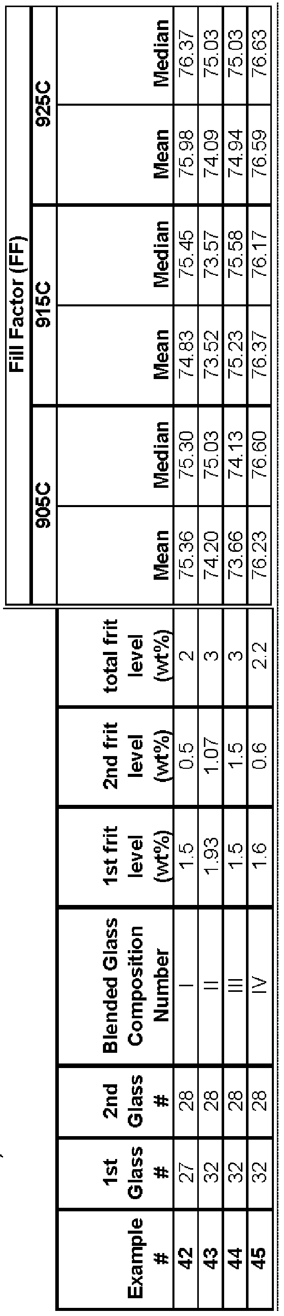
- Table 1 1 shows the combined frit composition of the examples of Table 1 2 and 1 3.
- the combined frit compositions shown in Table 1 1 are calculated using the frit compositions of Table 3 in the blending ratio of Tables 12 & 13.
- Solar cells for testing the performance of the thick-film paste were made from 175 micron thick Q.Cell multi-crystalline silicon wafers with a 65 ohm/sq phosphorous-doped emitter layer which had an acid-etched textured surface and 70 nm thick PECVD SiN x antireflective coating.
- the solar cells were supplied by Q-Cells SE, OT Thalheim, Germany.
- the wafers were cut into 28 mm x 28 mm wafers using a diamond wafering saw. Wafers were screen-printed after cut-down using an AMI-Presco MSP-485 screen printer to provide a bus-bar, eleven conductor lines at a 0.254 cm pitch, and a full ground-plane, screen-printed aluminum backside conductor. After printing and drying, cells were fired in a BTU
- the fired conductor line median line width was 120 microns and mean line height was 15 microns.
- the median line resistivity was 3.0E-6ohm cm. Performance of the 28 mm x 28 mm cells is expected to be impacted by edge effects that reduce the overall solar cell fill factor (FF) by - 5%.
- Pastes were applied to 1 .1 " x 1 .1 " dicing-saw-cut multi-crystalline silicon solar cells with a phosphorous-doped emitter on a p-type base.
- the paste from example #1 was applied to a DeutscheCell (DeutscheCell, Germany) multi-crystalline wafer with a 62 ⁇ / ⁇ emitter and pastes from examples #2 through #6 were applied to a Gintech (Gintech Energy Corporation, Taiwan) multi-crystalline wafer with a 55 ⁇ / ⁇ emitter.
- the solar cells used were textured by isotropic acid etching and had an anti- reflection coating (ARC) of SiNx:H. Efficiency and fill factor, as shown in Tables 9, 10, 1 2, & 13, were measured for each sample.
- each paste For each paste, the mean and median values of the efficiency and fill factor for 5 to 1 2 samples are shown. Each sample was made by screen-printing using a ETP model L555 printer set with a squeegee speed of 250 mm/sec. The screen used had a pattern of 1 1 finger lines with a 1 00 ⁇ opening and 1 bus bar with a 1 .5 mm opening on a 20 ⁇ emulsion in a screen with 325 mesh and 23 ⁇ wires. A commercially available Al paste, DuPont PV381 , was printed on the non-illuminated (back) side of the device. The device with the printed patterns on both sides was then dried for 10 minutes in a drying oven with a 250°C peak temperature.
- the substrates were then fired sun-side up with a CF7214 Despatch 6 zone IR furnace using a 560 cm/min belt speed and 550-600-650-700-800-905 to 945°C temperature set points.
- the actual temperature of the part was measured during processing.
- the estimated peak temperature of each part was 740-780°C and each part was above 650°C for a total time of 4 seconds.
- the fully processed samples were then tested for PV
- Solar cell performance was measured using a ST-1000, Telecom STV Co. I tester at 25 °C +/- 1 .0 °C.
- the Xe Arc lamp in the IV tester simulated sunlight with a known intensity, and irradiated the front surface of the cell.
- the tester used a four-contact method to measure current (I) and voltage (V) at approximately 400 load resistance settings to determine the cell's l-V curve.
- Solar cell efficiency (Eff), fill factor (FF), and series resistance (Rs) were calculated from the l-V curve. Rs is especially affected by contact resistivity (pc), conductor line resistance and emitter sheet resistance. Since conductor line resistances and sheet resistances were nominally equivalent for the various samples, the differences in Rs were primarily due to pc.
- Ideality factor was determined using the Suns- VOC technique. The ideality factor is reported at 0.1 sun irradiance.
- the solar cells built according to the method described herein were tested for conversion efficiency.
- An exemplary method of testing efficiency is provided below.
- the solar cells built according to the method described herein were placed in a commercial l-V tester for measuring efficiencies (Telecom STV, model ST-1000).
- the Xe Arc lamp in the l-V tester simulated the sunlight with a known intensity, AM 1 .5, and irradiated the front surface of the cell.
- the tester used a multi-point contact method to measure current (I) and voltage (V) at approximately 400 load resistance settings to determine the cell's l-V curve. Both fill factor (FF) and efficiency (Eff) were calculated from the l-V curve.
- Table 1 0 Paste fill factor (FF) data for the results of pastes using select frits of table 3
- Table 1 1 Combined frit composition resulting from the blended frit experiments of Tab es 12 and 13 using the frits from Table 3.
- Table 1 2 The paste efficiency (Eff%) results of paste using a blend of two different frits from table 3 (combined frit compositions given in Table 1 1 ).
- Table 1 3 The paste fill factor (FF) results of paste using a blend of two different frits from table 3 (combined frit compositions given in Table 1 1 ).
- a bismuth-tellurium-oxide (Bi-Te-O) containing composition as shown in table 14 was prepared using boron oxide (B2O3), zinc oxide
- Example I Lead-tellurium-oxide prepration of glass frits of Table 3.
- composition in the table are displayed as weight percent, based on the weight of the total glass composition
- Pastes using glass A were made by the following procedure.
- a paste was made by mixing the appropriate amount of organic vehicle (Table 4) and Ag powder.
- the Ag paste was passed through a 3-roll mill at progressively increasing pressures from 0 to 75 psi.
- the Ag paste viscosity was measured using a Brookfield viscometer and appropriate amounts of solvent and resin were added to adjust the paste viscosity toward a target of between 230 and 280 Pa-sec.
- Another paste was made by mixing the appropriate amount of organic vehicle (Table 4) and glass powder A.
- the frit paste was passed through a 3-roll mill at progressively increasing pressures from 0 to 250 psi.
- the degree of dispersion of each paste was measured by fineness of grind (FOG).
- a typical FOG value for a paste is less than 20 microns for the fourth longest, continuous scratch and less than 10 microns for the point at which 50% of the paste is scratched.
- the screen used had a pattern of 1 1 finger lines with a 1 00 ⁇ opening and 1 bus bar with a 1 .5 mm opening on a 20 ⁇ emulsion in a screen with 325 mesh and 23 ⁇ wires.
- a commercially available Al paste, DuPont PV381 was printed on the non-illuminated (back) side of the device.
- the device with the printed patterns on both sides was then dried for 10 minutes in a drying oven with a 250°C peak temperature.
- the actual temperature of the part was measured during processing.
- the estimated peak temperature of each part was 745-775°C and each part was above 650°C for a total time of 4 seconds.
- the fully processed samples were then tested for PV performance using a calibrated ST-1000 tester.
Abstract
Description


Claims
Priority Applications (8)
| Application Number | Priority Date | Filing Date | Title |
|---|---|---|---|
| KR1020127031582A KR20130016346A (en) | 2010-05-04 | 2011-05-04 | Thick-film pastes containing lead- and tellurium-oxides, and their use in the manufacture of semiconductor devices |
| CN201180031225.8A CN103038186B (en) | 2010-05-04 | 2011-05-04 | Include the thick film paste and its purposes in semiconductor device manufacture of lead oxides and tellurium oxide |
| JP2013509214A JP5782112B2 (en) | 2010-05-04 | 2011-05-04 | Thick film pastes containing lead and tellurium oxides and their use in the manufacture of semiconductor devices |
| KR1020157032496A KR20150133297A (en) | 2010-05-04 | 2011-05-04 | Thick-film pastes containing lead- and tellurium-oxides, and their use in the manufacture of semiconductor devices |
| ES11731163T ES2570133T3 (en) | 2010-05-04 | 2011-05-04 | Pastes in the form of a thick film containing lead and tellurium oxides and their use in the manufacture of semiconductor devices |
| KR1020187010658A KR102048388B1 (en) | 2010-05-04 | 2011-05-04 | Thick-film pastes containing lead- and tellurium-oxides, and their use in the manufacture of semiconductor devices |
| EP11731163.9A EP2566824B1 (en) | 2010-05-04 | 2011-05-04 | Thick-film pastes containing lead- and tellurium-oxides, and their use in the manufacture of semiconductor devices |
| KR1020197034102A KR102177050B1 (en) | 2010-05-04 | 2011-05-04 | Thick-film pastes containing lead- and tellurium-oxides, and their use in the manufacture of semiconductor devices |
Applications Claiming Priority (8)
| Application Number | Priority Date | Filing Date | Title |
|---|---|---|---|
| US33100610P | 2010-05-04 | 2010-05-04 | |
| US61/331,006 | 2010-05-04 | ||
| US201161440117P | 2011-02-07 | 2011-02-07 | |
| US61/440,117 | 2011-02-07 | ||
| US201161445508P | 2011-02-22 | 2011-02-22 | |
| US61/445,508 | 2011-02-22 | ||
| US201161467003P | 2011-03-24 | 2011-03-24 | |
| US61/467,003 | 2011-03-24 |
Publications (1)
| Publication Number | Publication Date |
|---|---|
| WO2011140197A1 true WO2011140197A1 (en) | 2011-11-10 |
Family
ID=44583755
Family Applications (5)
| Application Number | Title | Priority Date | Filing Date |
|---|---|---|---|
| PCT/US2011/035145 WO2011140192A1 (en) | 2010-05-04 | 2011-05-04 | Thick-film pastes containing lead-tellurium-lithium- oxides, and their use in the manufacture of semiconductor devices |
| PCT/US2011/035139 WO2011140189A1 (en) | 2010-05-04 | 2011-05-04 | Thick-film pastes containing lead-tellurium-boron-oxides, and their use in the manufacture of semiconductor devices |
| PCT/US2011/035167 WO2011140205A1 (en) | 2010-05-04 | 2011-05-04 | Thick-film pastes and solar cells made therefrom |
| PCT/US2011/035154 WO2011140197A1 (en) | 2010-05-04 | 2011-05-04 | Thick-film pastes containing lead- and tellurium-oxides, and their use in the manufacture of semiconductor devices |
| PCT/US2011/035131 WO2011140185A1 (en) | 2010-05-04 | 2011-05-04 | Thick-film pastes containing lead-tellurium-lithium-titanium-oxides, and their use in the manufacture of semiconductor devices |
Family Applications Before (3)
| Application Number | Title | Priority Date | Filing Date |
|---|---|---|---|
| PCT/US2011/035145 WO2011140192A1 (en) | 2010-05-04 | 2011-05-04 | Thick-film pastes containing lead-tellurium-lithium- oxides, and their use in the manufacture of semiconductor devices |
| PCT/US2011/035139 WO2011140189A1 (en) | 2010-05-04 | 2011-05-04 | Thick-film pastes containing lead-tellurium-boron-oxides, and their use in the manufacture of semiconductor devices |
| PCT/US2011/035167 WO2011140205A1 (en) | 2010-05-04 | 2011-05-04 | Thick-film pastes and solar cells made therefrom |
Family Applications After (1)
| Application Number | Title | Priority Date | Filing Date |
|---|---|---|---|
| PCT/US2011/035131 WO2011140185A1 (en) | 2010-05-04 | 2011-05-04 | Thick-film pastes containing lead-tellurium-lithium-titanium-oxides, and their use in the manufacture of semiconductor devices |
Country Status (9)
| Country | Link |
|---|---|
| US (12) | US8497420B2 (en) |
| EP (5) | EP2566824B1 (en) |
| JP (4) | JP5782112B2 (en) |
| KR (7) | KR101569567B1 (en) |
| CN (6) | CN103038186B (en) |
| ES (1) | ES2570133T3 (en) |
| HK (2) | HK1180295A1 (en) |
| TW (4) | TWI589649B (en) |
| WO (5) | WO2011140192A1 (en) |
Cited By (9)
| Publication number | Priority date | Publication date | Assignee | Title |
|---|---|---|---|---|
| JP2014028713A (en) * | 2012-07-31 | 2014-02-13 | Nippon Electric Glass Co Ltd | Glass for electrode formation and electrode formation material using the same |
| JP2014028740A (en) * | 2012-04-17 | 2014-02-13 | Heraeus Precious Metals North America Conshohocken Llc | Tellurium inorganic reaction system for thick electroconductive film paste for solar cell junction |
| CN103915127A (en) * | 2013-01-03 | 2014-07-09 | 上海匡宇电子技术有限公司 | Front silver paste for high sheet resistance silicon-based solar cell and preparing method of front silver paste |
| WO2014156964A1 (en) | 2013-03-29 | 2014-10-02 | 昭栄化学工業株式会社 | Conductive paste for solar cell element surface electrodes and method for manufacturing solar cell element |
| JP2014199926A (en) * | 2013-03-15 | 2014-10-23 | Dowaエレクトロニクス株式会社 | Calcination mold paste for solar cell electrode, solar cell, and silver powder |
| JP2014241348A (en) * | 2013-06-12 | 2014-12-25 | 株式会社ノリタケカンパニーリミテド | Paste composition for backside fire-through of solar battery, method for manufacturing solar battery, and solar battery |
| CN104756197A (en) * | 2012-12-21 | 2015-07-01 | 第一毛织株式会社 | Composition for forming solar cell electrode and electrode produced from same |
| KR101809698B1 (en) | 2009-07-03 | 2017-12-15 | 꼼미사리아 아 레네르지 아또미끄 에 오 에네르지 알떼르나띠브스 | Simplified copper-copper adhering method |
| US11464954B2 (en) | 2016-09-21 | 2022-10-11 | Cytrellis Biosystems, Inc. | Devices and methods for cosmetic skin resurfacing |
Families Citing this family (189)
| Publication number | Priority date | Publication date | Assignee | Title |
|---|---|---|---|---|
| JP5559510B2 (en) * | 2009-10-28 | 2014-07-23 | 昭栄化学工業株式会社 | Solar cell element and manufacturing method thereof |
| US8497420B2 (en) | 2010-05-04 | 2013-07-30 | E I Du Pont De Nemours And Company | Thick-film pastes containing lead- and tellurium-oxides, and their use in the manufacture of semiconductor devices |
| JP2013531894A (en) * | 2010-06-24 | 2013-08-08 | イー・アイ・デュポン・ドウ・ヌムール・アンド・カンパニー | Method for forming a silver back anode of a silicon solar cell |
| US9129725B2 (en) | 2010-12-17 | 2015-09-08 | E I Du Pont De Nemours And Company | Conductive paste composition containing lithium, and articles made therefrom |
| US8709862B2 (en) * | 2011-01-06 | 2014-04-29 | Heraeus Precious Metals North America Conshohocken Llc | Vanadium, cobalt and strontium additives for use in aluminum back solar cell contacts |
| US9680036B2 (en) * | 2011-01-06 | 2017-06-13 | Heraeus Precious Metals North America Conshohocken Llc | Organometallic and hydrocarbon additives for use with aluminum back solar cell contacts |
| US8815636B2 (en) * | 2011-01-06 | 2014-08-26 | Heraeus Precious Metals North America Conshohocken Llc | Oxides and glasses for use with aluminum back solar cell contacts |
| EP2689464A2 (en) * | 2011-03-24 | 2014-01-29 | E.I. Du Pont De Nemours And Company | Conductive paste composition and semiconductor devices made therewith |
| US8512463B2 (en) * | 2011-04-05 | 2013-08-20 | E I Du Pont De Nemours And Company | Thick film paste containing bismuth-tellurium-oxide and its use in the manufacture of semiconductor devices |
| JP5817827B2 (en) * | 2011-04-21 | 2015-11-18 | 昭栄化学工業株式会社 | Conductive paste |
| US8790550B2 (en) * | 2011-06-06 | 2014-07-29 | E I Du Pont De Nemours And Company | Low temperature fireable thick film silver paste |
| KR20140041865A (en) * | 2011-07-19 | 2014-04-04 | 히타치가세이가부시끼가이샤 | Composition that forms n-type diffusion layer, n-type diffusion layer manufacturing method and solar cell element manufacturing method |
| US8696948B2 (en) * | 2011-08-11 | 2014-04-15 | E I Du Pont De Nemours And Company | Thick film paste containing lead—tellurium—lithium—titanium—oxide and its use in the manufacture of semiconductor devices |
| US8691119B2 (en) * | 2011-08-11 | 2014-04-08 | E I Du Pont De Nemours And Company | Thick film paste containing lead-tellurium-lithium-titanium-oxide and its use in the manufacture of semiconductor devices |
| US8916069B2 (en) * | 2011-08-18 | 2014-12-23 | E I Du Pont De Nemours And Company | Conductive compositions containing rhodium and Pb-Te-O and their use in the manufacture of semiconductor devices |
| JP6068474B2 (en) * | 2011-09-09 | 2017-01-25 | ヘレウス プレシャス メタルズ ノース アメリカ コンショホーケン エルエルシー | Silver solar cell contacts |
| CN102315332B (en) * | 2011-09-29 | 2013-08-07 | 英利能源(中国)有限公司 | Heat treatment process of solar cell |
| US8771554B2 (en) * | 2011-10-20 | 2014-07-08 | E I Du Pont De Nemours And Company | Thick film silver paste containing Al2O3 and lead-tellurium—oxide and its use in the manufacture of semiconductor devices |
| EP2590177B1 (en) * | 2011-11-04 | 2015-08-12 | Heraeus Precious Metals North America Conshohocken LLC | Organic vehicle for electroconductive paste |
| US20130186463A1 (en) * | 2011-12-06 | 2013-07-25 | E I Du Pont De Nemours And Company | Conductive silver paste for a metal-wrap-through silicon solar cell |
| KR20130064659A (en) * | 2011-12-08 | 2013-06-18 | 제일모직주식회사 | Electrode paste composition for solar cell and electrode prepared using the same |
| KR101350960B1 (en) * | 2012-01-13 | 2014-01-16 | 한화케미칼 주식회사 | Glass frits, conductive paste composition comprising the same and solar cell |
| CN103204632B (en) * | 2012-01-14 | 2015-09-02 | 比亚迪股份有限公司 | Conductive glass powder and preparation method thereof, crystal silicon solar energy battery aluminum conductive electric slurry and preparation method |
| US20130180583A1 (en) * | 2012-01-17 | 2013-07-18 | E I Du Pont De Nemours And Company | Conductive paste for fine-line high-aspect-ratio screen printing in the manufacture of semiconductor devices |
| US8952245B2 (en) | 2012-01-23 | 2015-02-10 | Heraeus Precious Metals North America Conshohocken Llc | Conductive thick film paste for solar cell contacts |
| US8956557B2 (en) * | 2012-01-24 | 2015-02-17 | E I Du Pont De Nemours And Company | Thick film silver paste containing copper and lead—tellurium—oxide and its use in the manufacture of semiconductor devices |
| US9171972B2 (en) * | 2012-01-30 | 2015-10-27 | Kyocera Corporation | Method for producing photoelectric converter and phtotelectric converter |
| CN103377751B (en) * | 2012-04-17 | 2018-01-02 | 赫劳斯贵金属北美康舍霍肯有限责任公司 | Free conductive thick film paste for solar cell contact |
| CN103915128B (en) * | 2012-05-03 | 2016-06-08 | 苏州晶银新材料股份有限公司 | Photovoltaic cell back electrode electrocondution slurry |
| JP6359236B2 (en) * | 2012-05-07 | 2018-07-18 | トーカロ株式会社 | Electrostatic chuck |
| US9087937B2 (en) | 2012-05-10 | 2015-07-21 | E I Du Pont De Nemours And Company | Glass composition and its use in conductive silver paste |
| KR20150028811A (en) * | 2012-06-12 | 2015-03-16 | 헤레우스 프레셔스 메탈즈 노스 아메리카 콘쇼호켄 엘엘씨 | Electroconductive paste with adhesion enhancer |
| JP5937904B2 (en) * | 2012-06-26 | 2016-06-22 | 株式会社ノリタケカンパニーリミテド | Paste composition for solar cell electrode |
| JP5690780B2 (en) | 2012-07-18 | 2015-03-25 | 株式会社ノリタケカンパニーリミテド | Ag electrode forming paste composition, method for producing the same, and solar cell |
| US8652873B1 (en) | 2012-08-03 | 2014-02-18 | E I Du Pont De Nemours And Company | Thick-film paste containing lead-vanadium-based oxide and its use in the manufacture of semiconductor devices |
| KR20140022511A (en) * | 2012-08-13 | 2014-02-25 | 제일모직주식회사 | Electrode paste for solar cell, electrode prepared from the same and solar cell comprising the same |
| US8969709B2 (en) * | 2012-08-30 | 2015-03-03 | E I Du Pont De Nemours And Company | Use of a conductive composition containing lead—tellurium-based oxide in the manufacture of semiconductor devices with lightly doped emitters |
| US8900488B2 (en) * | 2012-09-06 | 2014-12-02 | E I Du Pont De Nemours And Company | Conductive paste composition and semiconductor devices made therewith |
| US9236161B2 (en) * | 2012-09-06 | 2016-01-12 | E I Du Pont De Nemours And Company | Conductive paste composition and semiconductor devices made therewith |
| JP2014060261A (en) * | 2012-09-18 | 2014-04-03 | Murata Mfg Co Ltd | Conductive paste, solar battery, and method for manufacturing solar battery |
| KR20160102091A (en) * | 2012-09-26 | 2016-08-26 | 헤레우스 프레셔스 메탈즈 노스 아메리카 콘쇼호켄 엘엘씨 | Conductive paste and solar cell |
| US10069021B2 (en) * | 2012-10-12 | 2018-09-04 | Heraeus Deutschland GmbH & Co. KG | Electro-conductive pastes with salts with an anion consisting of halogen and oxygen in solar cell applications |
| JP5756447B2 (en) * | 2012-10-31 | 2015-07-29 | 株式会社ノリタケカンパニーリミテド | Conductive paste composition for solar cell |
| KR101600652B1 (en) * | 2012-11-12 | 2016-03-07 | 제일모직주식회사 | Electrode paste for solar cell and electrode prepared thereof |
| KR101518500B1 (en) * | 2012-12-21 | 2015-05-11 | 제일모직주식회사 | Glass frit, electrode paste composition comprising the same, and electrode prepared using the same |
| WO2014146306A1 (en) * | 2013-03-22 | 2014-09-25 | 深圳首创光伏有限公司 | Conductive slurry of positive electrode of solar cell and preparing method thereof |
| JP5994650B2 (en) * | 2013-01-16 | 2016-09-21 | 昭栄化学工業株式会社 | Protective film forming glass composition and method for producing the same |
| JP6137852B2 (en) * | 2013-02-04 | 2017-05-31 | ナミックス株式会社 | Conductive paste for solar cell electrode formation |
| WO2014117409A1 (en) * | 2013-02-04 | 2014-08-07 | 深圳首创光伏有限公司 | Electrically conductive paste for positive electrode of crystalline silicon solar cell and preparation method thereof |
| US9236506B2 (en) * | 2013-02-05 | 2016-01-12 | E I Du Pont De Nemours And Company | Conductive silver paste for a metal-wrap-through silicon solar cell |
| KR101587683B1 (en) | 2013-02-15 | 2016-01-21 | 제일모직주식회사 | The composition for forming solar cell electrode comprising the same, and electrode prepared using the same |
| EP4092764A1 (en) | 2013-04-03 | 2022-11-23 | Lg Electronics Inc. | Solar cell |
| KR101882525B1 (en) | 2013-04-11 | 2018-07-26 | 삼성에스디아이 주식회사 | Composition for forming solar cell and electrode prepared using the same |
| KR101590224B1 (en) * | 2013-04-11 | 2016-01-29 | 제일모직주식회사 | Composition for forming solar cell electrode and electrode prepared using the same |
| KR101582374B1 (en) * | 2013-04-25 | 2016-01-04 | 제일모직주식회사 | Composition for forming solar cell electrode and electrode prepared using the same |
| KR101600659B1 (en) * | 2013-04-25 | 2016-03-07 | 제일모직주식회사 | Composition for forming solar cell electrode and electrode prepared using the same |
| KR101590226B1 (en) * | 2013-05-29 | 2016-01-29 | 제일모직주식회사 | Composition for forming solar cell electrode and electrode prepared using the same |
| US20140352768A1 (en) * | 2013-05-31 | 2014-12-04 | E I Du Pont De Nemours And Company | Method of manufacturing solar cell electrode |
| US9246027B2 (en) * | 2013-05-31 | 2016-01-26 | E I Du Pont De Nemours And Company | Method of manufacturing solar cell electrode |
| US9159864B2 (en) | 2013-07-25 | 2015-10-13 | First Solar, Inc. | Back contact paste with Te enrichment and copper doping control in thin film photovoltaic devices |
| KR101483875B1 (en) * | 2013-07-31 | 2015-01-16 | 삼성전기주식회사 | Glass core substrate and manufacturing method thereof |
| CN104347151A (en) * | 2013-08-02 | 2015-02-11 | 上海匡宇电子技术有限公司 | Conductive silver paste and preparation method thereof |
| CN103771715B (en) * | 2013-08-06 | 2017-09-05 | 浙江光达电子科技有限公司 | A kind of rear surface of solar cell silver paste glass dust and preparation method thereof |
| US8852995B1 (en) * | 2013-08-06 | 2014-10-07 | Atomic Energy Council-Institute Of Nuclear Energy Research | Preparation method for patternization of metal electrodes in silicon solar cells |
| KR101693070B1 (en) * | 2013-08-28 | 2017-01-04 | 제일모직주식회사 | Composition for forming solar cell electrode and electrode prepared using the same |
| US20150060742A1 (en) * | 2013-09-03 | 2015-03-05 | E I Du Pont De Nemours And Company | Conductive paste used for a solar cell electrode |
| KR101608123B1 (en) | 2013-09-13 | 2016-03-31 | 제일모직주식회사 | Composition for forming solar cell electrode and electrode prepared using the same |
| JP6142756B2 (en) * | 2013-10-02 | 2017-06-07 | セントラル硝子株式会社 | Glass powder material |
| CN103545015B (en) * | 2013-10-21 | 2016-08-24 | 深圳市首骋新材料科技有限公司 | Crystal silicon solar energy battery front electrode electrocondution slurry and preparation method thereof |
| CN103545016B (en) * | 2013-10-21 | 2016-06-29 | 深圳市首骋新材料科技有限公司 | Crystal silicon solar energy battery front electrode electrocondution slurry and preparation method thereof |
| CN104575661B (en) * | 2013-10-25 | 2017-09-12 | 硕禾电子材料股份有限公司 | Conductive paste and manufacturing method thereof |
| CN103545017B (en) * | 2013-10-25 | 2016-08-24 | 江苏昱星新材料科技有限公司 | A kind of conductive slurry for front electrode of solar battery and preparation method thereof |
| CN103606393B (en) * | 2013-11-08 | 2016-01-06 | 江苏科技大学 | A kind of solar battery back silver conductive silver paste composition and preparation method |
| KR101659131B1 (en) * | 2013-11-12 | 2016-09-22 | 제일모직주식회사 | Composition for forming solar cell electrode and electrode prepared using the same |
| KR101593754B1 (en) * | 2013-11-12 | 2016-02-12 | 제일모직주식회사 | Glass frit, composition for forming solar cell electrode comprising the same, and electrode prepared using the same |
| JP6114389B2 (en) * | 2013-11-20 | 2017-04-12 | 株式会社ノリタケカンパニーリミテド | Method for producing conductive composition |
| US9240515B2 (en) | 2013-11-25 | 2016-01-19 | E I Du Pont De Nemours And Company | Method of manufacturing a solar cell |
| CN103617843A (en) * | 2013-11-29 | 2014-03-05 | 江苏瑞德新能源科技有限公司 | Method for producing back silver paste |
| US9793025B2 (en) * | 2013-12-03 | 2017-10-17 | E I Du Pont De Nemours And Company | Conductive paste composition and semiconductor devices made therewith |
| JP6242198B2 (en) * | 2013-12-10 | 2017-12-06 | 京都エレックス株式会社 | Conductive paste for forming conductive film of semiconductor device, semiconductor device, and method for manufacturing semiconductor device |
| KR101780531B1 (en) * | 2013-12-17 | 2017-09-22 | 삼성에스디아이 주식회사 | Composition for forming solar cell electrode and electrode prepared using the same |
| US9039937B1 (en) | 2013-12-17 | 2015-05-26 | Samsung Sdi Co., Ltd. | Composition for solar cell electrodes and electrode fabricated using the same |
| KR20150072994A (en) * | 2013-12-20 | 2015-06-30 | 제일모직주식회사 | Composition for forming solar cell electrode and electrode prepared using the same |
| JP5903424B2 (en) * | 2013-12-21 | 2016-04-13 | 株式会社ノリタケカンパニーリミテド | Conductive paste composition for solar cell and method for producing the same |
| CN104751935A (en) * | 2013-12-26 | 2015-07-01 | 湖南利德电子浆料有限公司 | High-sheet-resistance efficient solar cell front silver paste and preparation method thereof |
| CN104751939B (en) * | 2013-12-31 | 2017-05-31 | 比亚迪股份有限公司 | A kind of crystal silicon solar energy battery aluminum conductive electric slurry |
| KR101696968B1 (en) * | 2014-01-09 | 2017-01-16 | 제일모직주식회사 | Composition for forming solar cell electrode and electrode prepared using the same |
| JP6046753B2 (en) * | 2014-01-17 | 2016-12-21 | ヘレウス プレシャス メタルズ ノース アメリカ コンショホーケン エルエルシー | Lead-bismuth-tellurium-silicate inorganic reaction system with improved adhesive properties |
| JP2015187063A (en) * | 2014-01-17 | 2015-10-29 | ヘレウス プレシャス メタルズ ノース アメリカ コンショホーケン エルエルシー | Lead-bismuth-tellurium inorganic reaction system for electroconductive paste composition |
| US20150206992A1 (en) * | 2014-01-17 | 2015-07-23 | Heraeus Precious Metals North America Conshohocken Llc | Lead-tellurium inorganic reaction systems |
| CN105939976A (en) * | 2014-01-28 | 2016-09-14 | 东进世美肯株式会社 | Glass composition and electrode composition for solar cell using same |
| US20150240099A1 (en) * | 2014-02-24 | 2015-08-27 | Xerox Corporation | Silver flake conductive paste ink with nickel particles |
| EP2913311B1 (en) * | 2014-02-26 | 2018-08-08 | Heraeus Precious Metals North America Conshohocken LLC | A glass comprising tungsten and lead in a solar cell paste |
| EP2913139B1 (en) * | 2014-02-26 | 2019-04-03 | Heraeus Precious Metals North America Conshohocken LLC | A glass comprising molybdenum and lead in a solar cell paste |
| US9761348B2 (en) | 2014-03-10 | 2017-09-12 | E I Du Pont De Nemours And Company | Conductive paste used for solar cell electrodes |
| CN103854721B (en) * | 2014-03-25 | 2016-04-13 | 中希集团有限公司 | A kind of solar battery front side metallization silver slurry and preparation method thereof |
| CN103951262B (en) * | 2014-04-15 | 2017-01-25 | 江苏欧耐尔新型材料有限公司 | Lead-tellurium-bismuth-containing glass paste for positive electrodes of solar cells as well as preparation and application methods of glass paste |
| GB201407418D0 (en) * | 2014-04-28 | 2014-06-11 | Johnson Matthey Plc | Conductive paste, electrode and solar cell |
| US9209323B2 (en) | 2014-05-05 | 2015-12-08 | E I Du Pont De Nemours And Company | Conductive paste used for solar cell electrodes and method of manufacturing the solar cell electrodes |
| CN105097067B (en) * | 2014-05-15 | 2017-11-14 | 三星Sdi株式会社 | For forming the composition of solar cel electrode and the electrode using its preparation |
| US9349883B2 (en) * | 2014-06-19 | 2016-05-24 | E I Du Pont De Nemours And Company | Conductor for a solar cell |
| CN104118992A (en) * | 2014-07-22 | 2014-10-29 | 江苏欧耐尔新型材料有限公司 | Glass powder for solar high-sheet-resistance paste and preparation method thereof |
| CN104150775A (en) * | 2014-08-01 | 2014-11-19 | 东华大学 | Low-melting-point tellurium glass used for photovoltaic cell conductive slurry and preparation method of low-melting-point tellurium glass |
| CN104193166B (en) * | 2014-09-05 | 2016-08-24 | 广东风华高新科技股份有限公司 | Frit and preparation method thereof |
| KR102219804B1 (en) | 2014-11-04 | 2021-02-24 | 엘지전자 주식회사 | Solar cell and the manufacturing mathod thereof |
| KR20160057583A (en) | 2014-11-13 | 2016-05-24 | 삼성에스디아이 주식회사 | Paste for forming solar cell electrode and electrode prepared using the same |
| JP5856277B1 (en) * | 2014-11-27 | 2016-02-09 | 株式会社ノリタケカンパニーリミテド | Solar cell electrode paste and solar cell |
| JP5816738B1 (en) * | 2014-11-27 | 2015-11-18 | 株式会社ノリタケカンパニーリミテド | Conductive composition |
| EP3509112B1 (en) | 2014-11-28 | 2020-10-14 | LG Electronics Inc. | Solar cell and method for manufacturing the same |
| TWI521546B (en) * | 2014-12-08 | 2016-02-11 | 碩禾電子材料股份有限公司 | A conductive paste containing lead-free glass frit |
| TWI521545B (en) * | 2014-12-08 | 2016-02-11 | 碩禾電子材料股份有限公司 | A conductive paste containing lead-free glass frit |
| CN104455923B (en) * | 2014-12-13 | 2016-10-05 | 常熟市华懋化工设备有限公司 | Enamel pipe fitting |
| JP2016115873A (en) * | 2014-12-17 | 2016-06-23 | 京都エレックス株式会社 | Conductive paste for forming solar cell electrode, and solar cell element and solar cell module using the same |
| CN104464884A (en) * | 2014-12-26 | 2015-03-25 | 常熟联茂电子科技有限公司 | Organic power resistance paste |
| CN104464890A (en) * | 2014-12-26 | 2015-03-25 | 常熟联茂电子科技有限公司 | Thick film circuit resistor paste |
| KR20160082468A (en) * | 2014-12-31 | 2016-07-08 | 헤레우스 프레셔스 메탈즈 노스 아메리카 콘쇼호켄 엘엘씨 | Glass compositions for electroconductive paste compositions |
| DE112016000610B4 (en) | 2015-02-04 | 2022-12-08 | Solar Paste, Llc | Electrically conductive paste composition, use of the same in a method of forming an electrically conductive structure, and an article, photovoltaic cell and semiconductor substrate comprising the paste composition |
| CN104692668B (en) * | 2015-02-11 | 2017-04-12 | 西北大学 | Rapid crystallization glass powder for positive electrode paste of solar cell |
| TWI532062B (en) * | 2015-04-27 | 2016-05-01 | Giga Solar Materials Corp | Conductive pulp and a method of manufacturing the same |
| JP2016213284A (en) * | 2015-05-01 | 2016-12-15 | 東洋アルミニウム株式会社 | Aluminum paste composition for PERC type solar cell |
| WO2016193209A1 (en) | 2015-06-02 | 2016-12-08 | Basf Se | Conductive paste and process for forming an electrode on a p-type emitter on an n-type base semiconductor substrate |
| JP6580383B2 (en) | 2015-06-17 | 2019-09-25 | ナミックス株式会社 | Conductive paste, solar cell, and method for manufacturing solar cell |
| KR102272433B1 (en) | 2015-06-30 | 2021-07-05 | 엘지전자 주식회사 | Solar cell and method of manufacturing the same |
| JP5990315B2 (en) * | 2015-09-17 | 2016-09-14 | 株式会社ノリタケカンパニーリミテド | Conductive composition |
| KR102507404B1 (en) * | 2015-09-25 | 2023-03-07 | 주식회사 엘지화학 | a crystallized powder for an electrode of a solar cell, a paste mixture and a solar cell thereof |
| KR101693840B1 (en) * | 2015-10-05 | 2017-01-09 | 대주전자재료 주식회사 | Paste composition for solar cell front electrode and solar cell using thereof |
| KR101940170B1 (en) * | 2015-10-22 | 2019-01-18 | 삼성에스디아이 주식회사 | Composition forforming electrode, electrode manufactured using the same and solar cell |
| US9741878B2 (en) | 2015-11-24 | 2017-08-22 | PLANT PV, Inc. | Solar cells and modules with fired multilayer stacks |
| CN105632589A (en) * | 2016-03-18 | 2016-06-01 | 苏州开元民生科技股份有限公司 | High heat storage crystal silicon solar back electrode silver paste and preparation method therefor |
| US20170291846A1 (en) * | 2016-04-07 | 2017-10-12 | Heraeus Precious Metals North America Conshohocken Llc | Halogenide containing glasses in metallization pastes for silicon solar cells |
| US10134925B2 (en) | 2016-04-13 | 2018-11-20 | E I Du Pont De Nemours And Company | Conductive paste composition and semiconductor devices made therewith |
| DE102017003604A1 (en) | 2016-04-13 | 2017-10-19 | E.I. Du Pont De Nemours And Company | Conductive paste composition and semiconductor devices made therewith |
| JP6830524B2 (en) | 2016-08-03 | 2021-02-17 | フエロ コーポレーション | Passivation glass for semiconductor devices |
| WO2018032351A1 (en) * | 2016-08-16 | 2018-02-22 | Zhejiang Kaiying New Materials Co., Ltd. | Thick-film paste for front-side metallization in silicon solar cells |
| US10741300B2 (en) | 2016-10-07 | 2020-08-11 | E I Du Pont De Nemours And Company | Conductive paste composition and semiconductor devices made therewith |
| US10593439B2 (en) | 2016-10-21 | 2020-03-17 | Dupont Electronics, Inc. | Conductive paste composition and semiconductor devices made therewith |
| KR20180046808A (en) * | 2016-10-28 | 2018-05-09 | 삼성에스디아이 주식회사 | Composition for forming solar cell electrode and electrode prepared using the same |
| KR101853417B1 (en) * | 2016-11-24 | 2018-05-02 | 엘에스니꼬동제련 주식회사 | Conductive paste composition for electrode of solar cell and solar cell comprising electrode manufactured using the same |
| MY190562A (en) | 2016-12-20 | 2022-04-27 | Zhejiang Kaiying New Mat Co Ltd | Interdigitated back contact metal-insulator-semiconductor solar cell with printed oxide tunnel junctions |
| CN108885917B (en) | 2016-12-20 | 2020-06-02 | 浙江凯盈新材料有限公司 | Silicone-containing solar cell metallization paste |
| WO2018149802A1 (en) | 2017-02-15 | 2018-08-23 | Basf Se | Glass frit, conductive paste and use of the conductive paste |
| US10115505B2 (en) * | 2017-02-23 | 2018-10-30 | E I Du Pont De Nemours And Company | Chip resistor |
| US9847437B1 (en) | 2017-03-21 | 2017-12-19 | Jiun Pyng You | Method of forming conductive electrode grids over silicon wafer surfaces |
| TWI745562B (en) * | 2017-04-18 | 2021-11-11 | 美商太陽帕斯特有限責任公司 | Conductive paste composition and semiconductor devices made therewith |
| KR102290565B1 (en) * | 2017-04-28 | 2021-08-18 | 한국전자기술연구원 | Multi-layer structure and manufacturing method thereof |
| TWI638793B (en) * | 2017-04-28 | 2018-10-21 | 碩禾電子材料股份有限公司 | Conductive paste for solar cell, solar cell and manufacturing method thereof, and solar cell module |
| CN107274963B (en) * | 2017-05-31 | 2019-05-24 | 深圳磐汩新能源有限公司 | Silicon solar cell front side conductive silver paste and preparation method thereof |
| KR101972384B1 (en) * | 2017-09-08 | 2019-08-19 | 대주전자재료 주식회사 | Paste composition of solar cell front electrode and manufacturing method thereof |
| US10040717B1 (en) * | 2017-09-18 | 2018-08-07 | Jiangxi Jiayin Science and Technology, Ltd. | Thick-film paste with multiple discrete frits and methods for contacting crystalline silicon solar cell emitter surfaces |
| CN107759092B (en) * | 2017-09-28 | 2020-12-22 | 浙江光达电子科技有限公司 | Lead-free glass powder for back passivation of crystalline silicon solar cell back silver paste and preparation method thereof |
| JP7103366B2 (en) * | 2017-10-03 | 2022-07-20 | 昭栄化学工業株式会社 | Conductive paste for forming solar cell electrodes |
| CN107746184B (en) * | 2017-10-20 | 2020-11-24 | 苏州晶银新材料股份有限公司 | Glass powder composition, conductive silver paste containing glass powder composition and preparation method of conductive silver paste |
| CN107759093B (en) * | 2017-10-23 | 2020-05-22 | 常州聚和新材料股份有限公司 | Glass material for high sheet resistance shallow crystalline silicon solar cell, preparation method thereof and slurry |
| CN107812527B (en) * | 2017-11-09 | 2020-08-07 | 南京大学(苏州)高新技术研究院 | Preparation and application of powder catalytic material and graphite-phase-containing carbon nitride composite nano catalytic material |
| CN110603648B (en) * | 2018-03-30 | 2022-06-17 | 深圳市首骋新材料科技有限公司 | Crystalline silicon solar cell front conductive paste and preparation method thereof and solar cell |
| CN112041994B (en) | 2018-03-30 | 2022-06-21 | 深圳市首骋新材料科技有限公司 | Crystalline silicon solar cell front conductive paste and preparation method thereof and solar cell |
| FR3080708B1 (en) * | 2018-04-27 | 2020-04-24 | Silec Cable | INSULATOR FOR A CABLE END |
| JP2019214494A (en) * | 2018-06-13 | 2019-12-19 | 国立大学法人 鹿児島大学 | Glass, glass paste, and manufacturing method of glass |
| CN110808304A (en) * | 2018-07-20 | 2020-02-18 | 张伟 | Photovoltaic module with pattern and preparation method thereof |
| US11152640B2 (en) * | 2018-10-05 | 2021-10-19 | University Of Maryland | Lithium bismuth oxide compounds as Li super-ionic conductor, solid electrolyte, and coating layer for Li metal battery and Li-ion battery |
| KR102316662B1 (en) * | 2018-10-10 | 2021-10-25 | 창저우 퓨전 뉴 머티리얼 씨오. 엘티디. | Method for forming solar cell electrode, solar cell electrode manufactured therefrom and solar cell |
| CN109336594B (en) * | 2018-10-26 | 2021-10-01 | 贵州振华电子信息产业技术研究有限公司 | Low-capacitance change rate piezoelectric ceramic element, piezoelectric ceramic and manufacturing method thereof |
| CN111302636A (en) * | 2018-12-11 | 2020-06-19 | 苏州晶银新材料股份有限公司 | Glass powder composition, conductive silver paste containing glass powder composition and solar cell |
| CN111302620A (en) * | 2018-12-11 | 2020-06-19 | 苏州晶银新材料股份有限公司 | Glass powder composition, conductive silver paste containing glass powder composition and solar cell |
| CN111354503A (en) * | 2018-12-24 | 2020-06-30 | 东泰高科装备科技有限公司 | Conductive silver paste for flexible thin-film solar cell module and preparation method thereof |
| TWI697015B (en) * | 2019-03-05 | 2020-06-21 | 南韓商大州電子材料股份有限公司 | Paste composition of solar cell front electrode and manufacturing method thereof |
| CN110002758A (en) * | 2019-04-17 | 2019-07-12 | 北京大学深圳研究生院 | For the glass powder of silver paste of solar cells, silver paste and its preparation method and application |
| CN110015851A (en) * | 2019-04-17 | 2019-07-16 | 北京大学深圳研究生院 | A kind of glass powder being used to prepare silver paste of solar cells and its application |
| CN109970347A (en) * | 2019-04-29 | 2019-07-05 | 齐鲁工业大学 | A kind of TeO improving performance of lithium ion battery2-V2O5- CuO devitrified glass negative electrode material |
| CN110092577B (en) * | 2019-05-21 | 2022-03-22 | 张学新 | Preparation method of high borosilicate red glass tube |
| US10622502B1 (en) | 2019-05-23 | 2020-04-14 | Zhejiang Kaiying New Materials Co., Ltd. | Solar cell edge interconnects |
| US10749045B1 (en) | 2019-05-23 | 2020-08-18 | Zhejiang Kaiying New Materials Co., Ltd. | Solar cell side surface interconnects |
| US11508862B2 (en) | 2019-05-29 | 2022-11-22 | Changzhou Fusion New Material Co., Ltd. | Thick-film conductive paste, and their use in the manufacture of solar cells |
| CN110342827A (en) * | 2019-06-21 | 2019-10-18 | 浙江中希电子科技有限公司 | A kind of low temperature modification glass powder and its application in the dual layer passivation Perc battery of front |
| CN110305523A (en) * | 2019-07-02 | 2019-10-08 | 黄山市晶特美新材料有限公司 | A kind of silk-screen impact-resistant glass ink and preparation method thereof |
| CN110451805B (en) * | 2019-09-19 | 2021-11-26 | 成都光明光电有限责任公司 | Sealing glass |
| CN110467448B (en) * | 2019-09-19 | 2021-12-07 | 安徽建筑大学 | Preparation method of nano NTC ceramic powder suitable for tape casting and tape casting film |
| KR102238252B1 (en) * | 2019-10-24 | 2021-04-09 | 주식회사 베이스 | Glass frit and electrode paste composition for solar cell comprising the same |
| KR102283727B1 (en) * | 2020-01-21 | 2021-08-02 | 박태호 | Glass frit and electrode paste composition for solar cell comprising the same |
| CN111768892B (en) * | 2020-07-21 | 2021-12-21 | 西安宏星电子浆料科技股份有限公司 | Acid-resistant electroplatable conductor paste for aluminum nitride matrix |
| CN111848165B (en) * | 2020-08-03 | 2021-04-09 | 深圳见炬科技有限公司 | P-type bismuth telluride thermoelectric material and preparation method thereof |
| CN112028487A (en) * | 2020-09-25 | 2020-12-04 | 广东四通集团股份有限公司 | Preparation method of wear-resistant glaze daily porcelain glaze |
| CN112635593B (en) * | 2020-12-22 | 2022-05-24 | 东北电力大学 | All-antimony-based thin film solar cell and preparation method thereof |
| CN113072303A (en) * | 2021-03-29 | 2021-07-06 | 浙江奕成科技有限公司 | Shape changing method of glass powder for solar cell conductive silver paste |
| CN112992401B (en) * | 2021-04-25 | 2021-09-03 | 西安宏星电子浆料科技股份有限公司 | Resistance paste capable of realizing lossless resistance adjustment |
| CN114133231A (en) * | 2021-11-05 | 2022-03-04 | 深圳顺络电子股份有限公司 | Nickel-zinc ferrite material and method for producing same |
| CN114409248B (en) * | 2022-01-06 | 2023-04-07 | 江苏日御光伏新材料科技有限公司 | Low-heat-loss tellurium-lithium-silicon-zirconium system glass material, and conductive paste and application thereof |
| CN115504769B (en) * | 2022-10-21 | 2023-11-03 | 无锡市高宇晟新材料科技有限公司 | Microwave dielectric ceramic material and preparation method and application thereof |
| CN116741431B (en) * | 2023-08-09 | 2023-11-14 | 常州聚和新材料股份有限公司 | Thin gate silver paste suitable for thin Poly layer on back of N-type TOPCO battery and preparation method thereof |
Citations (2)
| Publication number | Priority date | Publication date | Assignee | Title |
|---|---|---|---|---|
| EP0463826A1 (en) * | 1990-06-21 | 1992-01-02 | Johnson Matthey Inc. | Sealing glass composition and electrically conductive formulation containing same |
| WO1992000925A1 (en) * | 1990-07-09 | 1992-01-23 | Cookson Group Plc | Glass compositions |
Family Cites Families (91)
| Publication number | Priority date | Publication date | Assignee | Title |
|---|---|---|---|---|
| GB736073A (en) * | 1955-01-26 | 1955-08-31 | British Thomson Houston Co Ltd | Improvements in glass compositions |
| JPS5480596A (en) * | 1977-12-09 | 1979-06-27 | Matsushita Electric Ind Co Ltd | Varistor |
| US4293451A (en) | 1978-06-08 | 1981-10-06 | Bernd Ross | Screenable contact structure and method for semiconductor devices |
| US4401767A (en) * | 1981-08-03 | 1983-08-30 | Johnson Matthey Inc. | Silver-filled glass |
| JPS5933869A (en) | 1982-08-20 | 1984-02-23 | Hitachi Ltd | Electrode material for semiconductor device |
| JPS60140880A (en) | 1983-12-28 | 1985-07-25 | Hitachi Ltd | Manufacture of solar cell |
| JPS6236040A (en) * | 1985-08-08 | 1987-02-17 | Iwaki Glass Kk | Low-melting point sealing glass |
| JPH01138150A (en) | 1987-11-25 | 1989-05-31 | Ohara Inc | Low-melting glass |
| US4945071A (en) | 1989-04-19 | 1990-07-31 | National Starch And Chemical Investment Holding Company | Low softening point metallic oxide glasses suitable for use in electronic applications |
| US5245492A (en) * | 1989-11-28 | 1993-09-14 | Matsushita Electric Industrial Co., Ltd. | Magnetic head |
| JPH03218943A (en) * | 1989-11-28 | 1991-09-26 | Matsushita Electric Ind Co Ltd | Sealing glass |
| US5013697A (en) * | 1990-06-21 | 1991-05-07 | Johnson Matthey Inc. | Sealing glass compositions |
| US5066621A (en) * | 1990-06-21 | 1991-11-19 | Johnson Matthey Inc. | Sealing glass composition and electrically conductive formulation containing same |
| US5118362A (en) * | 1990-09-24 | 1992-06-02 | Mobil Solar Energy Corporation | Electrical contacts and methods of manufacturing same |
| JPH0762557B2 (en) | 1991-07-02 | 1995-07-05 | 株式会社ノーリツ | Air conditioner installation device |
| US5240884A (en) * | 1991-09-05 | 1993-08-31 | Johnson Matthey, Inc. | Silver-glass die attach paste |
| JP3148303B2 (en) | 1991-10-18 | 2001-03-19 | 株式会社住田光学ガラス | Manufacturing method of optical fiber bundle for heat and vacuum resistance |
| US5188990A (en) * | 1991-11-21 | 1993-02-23 | Vlsi Packaging Materials | Low temperature sealing glass compositions |
| JPH05175254A (en) | 1991-12-20 | 1993-07-13 | Nippon Electric Glass Co Ltd | Low melting point bonding composition |
| DE69326655T2 (en) * | 1992-02-25 | 2000-05-18 | Matsushita Electric Ind Co Ltd | ZINCOXIDE VARISTOR AND ITS PRODUCTION |
| JPH05259201A (en) * | 1992-03-11 | 1993-10-08 | Nec Corp | Semiconductor device and its production |
| US5334558A (en) | 1992-10-19 | 1994-08-02 | Diemat, Inc. | Low temperature glass with improved thermal stress properties and method of use |
| US5663109A (en) | 1992-10-19 | 1997-09-02 | Quantum Materials, Inc. | Low temperature glass paste with high metal to glass ratio |
| US5336644A (en) * | 1993-07-09 | 1994-08-09 | Johnson Matthey Inc. | Sealing glass compositions |
| JPH0897011A (en) * | 1994-09-26 | 1996-04-12 | Matsushita Electric Ind Co Ltd | Electrode material for zinc oxide varistor |
| JP3541070B2 (en) * | 1994-11-15 | 2004-07-07 | イー・アイ・デュポン・ドウ・ヌムール・アンド・カンパニー | Automotive glass thick film conductor paste |
| JP3624482B2 (en) * | 1995-09-22 | 2005-03-02 | 株式会社村田製作所 | Conductive paste and fluorescent display tube using the same |
| US5820639A (en) * | 1996-09-20 | 1998-10-13 | Bolder Technologies Corporation | Method of manufacturing lead acid cell paste having tin compounds |
| JPH10340621A (en) | 1997-06-05 | 1998-12-22 | Tanaka Kikinzoku Kogyo Kk | Conductive paste |
| JP3740251B2 (en) * | 1997-06-09 | 2006-02-01 | キヤノン株式会社 | Manufacturing method of solar cell module |
| US6350915B1 (en) | 1999-06-11 | 2002-02-26 | Merck & Co., Inc. | Process for the synthesis of 1-(3,5-bis(trifluoromethyl)-phenyl)ethan-1-one |
| JP2001284754A (en) | 2000-03-30 | 2001-10-12 | Kyocera Corp | Glass ceramic circuit board |
| JP2001313400A (en) | 2000-04-28 | 2001-11-09 | Kyocera Corp | Method for forming solar battery element |
| JP4487596B2 (en) | 2004-02-27 | 2010-06-23 | Tdk株式会社 | Method for manufacturing multilayer unit for multilayer ceramic electronic component |
| JP4846219B2 (en) | 2004-09-24 | 2011-12-28 | シャープ株式会社 | Method for manufacturing crystalline silicon solar cell |
| US20060102228A1 (en) | 2004-11-12 | 2006-05-18 | Ferro Corporation | Method of making solar cell contacts |
| US7462304B2 (en) | 2005-04-14 | 2008-12-09 | E.I. Du Pont De Nemours And Company | Conductive compositions used in the manufacture of semiconductor device |
| US7494607B2 (en) * | 2005-04-14 | 2009-02-24 | E.I. Du Pont De Nemours And Company | Electroconductive thick film composition(s), electrode(s), and semiconductor device(s) formed therefrom |
| US7556748B2 (en) * | 2005-04-14 | 2009-07-07 | E. I. Du Pont De Nemours And Company | Method of manufacture of semiconductor device and conductive compositions used therein |
| US7435361B2 (en) | 2005-04-14 | 2008-10-14 | E.I. Du Pont De Nemours And Company | Conductive compositions and processes for use in the manufacture of semiconductor devices |
| US8093491B2 (en) | 2005-06-03 | 2012-01-10 | Ferro Corporation | Lead free solar cell contacts |
| US7771623B2 (en) * | 2005-06-07 | 2010-08-10 | E.I. du Pont de Nemours and Company Dupont (UK) Limited | Aluminum thick film composition(s), electrode(s), semiconductor device(s) and methods of making thereof |
| KR100685845B1 (en) * | 2005-10-21 | 2007-02-22 | 삼성에스디아이 주식회사 | Organic eletroluminescence display device and method for fabricating of the same |
| JP5152518B2 (en) | 2006-03-10 | 2013-02-27 | 日産化学工業株式会社 | Substituted isoxazoline compounds and pest control agents |
| US20090095344A1 (en) | 2006-04-25 | 2009-04-16 | Tomohiro Machida | Conductive Paste for Solar Cell Electrode |
| US7783195B2 (en) * | 2006-07-07 | 2010-08-24 | Scientific-Atlanta, Llc | Format converter with smart multitap with digital forward and reverse |
| JP4918182B2 (en) | 2006-09-26 | 2012-04-18 | Hoya株式会社 | Manufacturing method and manufacturing apparatus for glass molded body, and manufacturing method for optical element |
| CN101164943A (en) * | 2006-10-19 | 2008-04-23 | 北京印刷学院 | Leadless tellurate low melting glass used as cementation phase in electronic slurry |
| CN100408256C (en) * | 2006-11-26 | 2008-08-06 | 常熟市华银焊料有限公司 | Cadmium-free silver solder containing gallium, indium and cerium |
| JP5091161B2 (en) | 2006-12-26 | 2012-12-05 | 京セラ株式会社 | Solar cell element and method for manufacturing solar cell element |
| KR100787463B1 (en) | 2007-01-05 | 2007-12-26 | 삼성에스디아이 주식회사 | A glass frit, a composition for preparing seal material and a light emitting device |
| JP5220335B2 (en) | 2007-04-11 | 2013-06-26 | 信越化学工業株式会社 | Manufacturing method of SOI substrate |
| US7731868B2 (en) * | 2007-04-12 | 2010-06-08 | E.I. Du Pont De Nemours And Company | Thick film conductive composition and process for use in the manufacture of semiconductor device |
| JP5530920B2 (en) | 2007-04-25 | 2014-06-25 | ヘレウス プレシャス メタルズ ノース アメリカ コンショホーケン エルエルシー | Formation of thick film conductor made of silver and nickel, or silver and nickel alloy, and solar cell made therefrom |
| JP5272373B2 (en) * | 2007-10-17 | 2013-08-28 | セントラル硝子株式会社 | Polycrystalline Si solar cell |
| JP2009099871A (en) * | 2007-10-18 | 2009-05-07 | Toppan Printing Co Ltd | Lead frame and manufacturing method thereof, and resin-sealed semiconductor device and manufacturing method thereof |
| WO2009052356A2 (en) | 2007-10-18 | 2009-04-23 | E. I. Du Pont De Nemours And Company | Conductive compositions and processes for use in the manufacture of semiconductor devices |
| US7736546B2 (en) | 2008-01-30 | 2010-06-15 | Basf Se | Glass frits |
| JP5525714B2 (en) | 2008-02-08 | 2014-06-18 | 日立粉末冶金株式会社 | Glass composition |
| CN101981630A (en) * | 2008-04-09 | 2011-02-23 | E.I.内穆尔杜邦公司 | Conductive compositions and processes for use in the manufacture of semiconductor devices |
| US7608206B1 (en) | 2008-04-18 | 2009-10-27 | E.I. Dupont De Nemours & Company | Non-lead resistor composition |
| US8158504B2 (en) * | 2008-05-30 | 2012-04-17 | E. I. Du Pont De Nemours And Company | Conductive compositions and processes for use in the manufacture of semiconductor devices—organic medium components |
| WO2010016186A1 (en) | 2008-08-07 | 2010-02-11 | 京都エレックス株式会社 | Conductive paste for formation of a solar cell element electrode, solar cell element, and manufacturing method for said solar cell element |
| JP5414409B2 (en) | 2009-01-16 | 2014-02-12 | 日立粉末冶金株式会社 | Low melting glass composition, low-temperature sealing material and electronic component using the same |
| WO2010109541A1 (en) | 2009-03-27 | 2010-09-30 | 株式会社日立製作所 | Conductive paste and electronic part equipped with electrode wiring formed from same |
| TWI391362B (en) | 2009-03-27 | 2013-04-01 | Hitachi Powdered Metals | A glass composition and a conductive mortar composition using the same, an electrode wire member, and an electronic component |
| JP5567785B2 (en) | 2009-03-31 | 2014-08-06 | 三菱マテリアル株式会社 | Conductive composition and method for producing solar cell using the same |
| JP2010251645A (en) | 2009-04-20 | 2010-11-04 | Namics Corp | Solar cell, and conductive paste for forming electrode of the same |
| WO2010123967A2 (en) | 2009-04-22 | 2010-10-28 | E. I. Du Pont De Nemours And Company | Glass compositions used in conductors for photovoltaic cells |
| US7910393B2 (en) | 2009-06-17 | 2011-03-22 | Innovalight, Inc. | Methods for forming a dual-doped emitter on a silicon substrate with a sub-critical shear thinning nanoparticle fluid |
| JP2011018425A (en) | 2009-07-10 | 2011-01-27 | Showa Denko Kk | Method for manufacturing magnetic recording medium, and magnetic recording and playback device |
| JP5559509B2 (en) * | 2009-10-28 | 2014-07-23 | 昭栄化学工業株式会社 | Conductive paste for solar cell electrode formation |
| JP5559510B2 (en) | 2009-10-28 | 2014-07-23 | 昭栄化学工業株式会社 | Solar cell element and manufacturing method thereof |
| CN102770963B (en) | 2010-02-08 | 2016-02-03 | E·I·内穆尔杜邦公司 | For the preparation of the method for MWT silicon solar cell |
| US8497420B2 (en) | 2010-05-04 | 2013-07-30 | E I Du Pont De Nemours And Company | Thick-film pastes containing lead- and tellurium-oxides, and their use in the manufacture of semiconductor devices |
| WO2012099877A1 (en) | 2011-01-18 | 2012-07-26 | Heraeus Precious Metals North America Conshohocken Llc | Electroconductive paste compositions and solar cell electrodes and contacts made therefrom |
| US20130049148A1 (en) | 2011-02-22 | 2013-02-28 | E I Du Pont De Nemours And Company | Conductive paste composition and semiconductor devices made therewith |
| JP5048142B2 (en) | 2011-03-04 | 2012-10-17 | 日本電産コパル株式会社 | Camera device |
| EP2689464A2 (en) | 2011-03-24 | 2014-01-29 | E.I. Du Pont De Nemours And Company | Conductive paste composition and semiconductor devices made therewith |
| US8512463B2 (en) | 2011-04-05 | 2013-08-20 | E I Du Pont De Nemours And Company | Thick film paste containing bismuth-tellurium-oxide and its use in the manufacture of semiconductor devices |
| US8696948B2 (en) | 2011-08-11 | 2014-04-15 | E I Du Pont De Nemours And Company | Thick film paste containing lead—tellurium—lithium—titanium—oxide and its use in the manufacture of semiconductor devices |
| US9023254B2 (en) | 2011-10-20 | 2015-05-05 | E I Du Pont De Nemours And Company | Thick film silver paste and its use in the manufacture of semiconductor devices |
| US8771554B2 (en) | 2011-10-20 | 2014-07-08 | E I Du Pont De Nemours And Company | Thick film silver paste containing Al2O3 and lead-tellurium—oxide and its use in the manufacture of semiconductor devices |
| US20130186463A1 (en) | 2011-12-06 | 2013-07-25 | E I Du Pont De Nemours And Company | Conductive silver paste for a metal-wrap-through silicon solar cell |
| CN102496404B (en) | 2011-12-27 | 2013-10-30 | 华东理工大学 | Electrode silver paste used by high efficiency crystal silicon solar cell |
| US9087937B2 (en) | 2012-05-10 | 2015-07-21 | E I Du Pont De Nemours And Company | Glass composition and its use in conductive silver paste |
| US8969709B2 (en) | 2012-08-30 | 2015-03-03 | E I Du Pont De Nemours And Company | Use of a conductive composition containing lead—tellurium-based oxide in the manufacture of semiconductor devices with lightly doped emitters |
| JP5756447B2 (en) | 2012-10-31 | 2015-07-29 | 株式会社ノリタケカンパニーリミテド | Conductive paste composition for solar cell |
| JP2015216355A (en) | 2014-04-23 | 2015-12-03 | 日東電工株式会社 | Wavelength conversion member and method of manufacturing the same |
| CN104726085A (en) | 2014-07-02 | 2015-06-24 | 济南大学 | Core-shell structured quantum dot composite nanocrystalline fluorescence probe and preparation method thereof |
| TWI745562B (en) | 2017-04-18 | 2021-11-11 | 美商太陽帕斯特有限責任公司 | Conductive paste composition and semiconductor devices made therewith |
-
2011
- 2011-05-04 US US13/100,533 patent/US8497420B2/en active Active
- 2011-05-04 ES ES11731163T patent/ES2570133T3/en active Active
- 2011-05-04 US US13/100,540 patent/US8889979B2/en active Active
- 2011-05-04 KR KR1020127031580A patent/KR101569567B1/en active IP Right Grant
- 2011-05-04 EP EP11731163.9A patent/EP2566824B1/en active Active
- 2011-05-04 KR KR1020197034102A patent/KR102177050B1/en active IP Right Grant
- 2011-05-04 TW TW100115700A patent/TWI589649B/en active
- 2011-05-04 WO PCT/US2011/035145 patent/WO2011140192A1/en active Application Filing
- 2011-05-04 CN CN201180031225.8A patent/CN103038186B/en active Active
- 2011-05-04 US US13/100,563 patent/US8889980B2/en active Active
- 2011-05-04 CN CN201180032359.1A patent/CN102958861B/en active Active
- 2011-05-04 EP EP11731539.0A patent/EP2566826B1/en active Active
- 2011-05-04 EP EP11731537.4A patent/EP2566825B1/en active Active
- 2011-05-04 CN CN201180031184.2A patent/CN102947235B/en active Active
- 2011-05-04 CN CN201710681515.6A patent/CN107424662B/en active Active
- 2011-05-04 KR KR1020127031579A patent/KR101569566B1/en active IP Right Grant
- 2011-05-04 EP EP11731162.1A patent/EP2566823B1/en active Active
- 2011-05-04 TW TW100115704A patent/TWI611428B/en active
- 2011-05-04 JP JP2013509214A patent/JP5782112B2/en active Active
- 2011-05-04 CN CN201180032701.8A patent/CN102971268B/en active Active
- 2011-05-04 JP JP2013509212A patent/JP5480448B2/en active Active
- 2011-05-04 US US13/100,619 patent/US20110232747A1/en not_active Abandoned
- 2011-05-04 JP JP2013509210A patent/JP5746325B2/en active Active
- 2011-05-04 JP JP2013509209A patent/JP5711359B2/en active Active
- 2011-05-04 KR KR1020187010658A patent/KR102048388B1/en active IP Right Grant
- 2011-05-04 KR KR1020127031582A patent/KR20130016346A/en not_active Application Discontinuation
- 2011-05-04 WO PCT/US2011/035139 patent/WO2011140189A1/en active Application Filing
- 2011-05-04 WO PCT/US2011/035167 patent/WO2011140205A1/en active Application Filing
- 2011-05-04 TW TW100115703A patent/TWI564351B/en active
- 2011-05-04 EP EP16154516.5A patent/EP3070062A1/en active Pending
- 2011-05-04 US US13/100,550 patent/US8895843B2/en active Active
- 2011-05-04 TW TW100115705A patent/TWI498308B/en active
- 2011-05-04 WO PCT/US2011/035154 patent/WO2011140197A1/en active Application Filing
- 2011-05-04 KR KR1020157032496A patent/KR20150133297A/en not_active Application Discontinuation
- 2011-05-04 CN CN201811172520.5A patent/CN109014180B/en active Active
- 2011-05-04 WO PCT/US2011/035131 patent/WO2011140185A1/en active Application Filing
- 2011-05-04 KR KR1020127031581A patent/KR101569568B1/en active IP Right Grant
-
2013
- 2013-03-13 US US13/801,036 patent/US20130255769A1/en not_active Abandoned
- 2013-03-13 US US13/801,248 patent/US9722100B2/en active Active
- 2013-03-13 US US13/800,592 patent/US10069020B2/en active Active
- 2013-03-13 US US13/800,861 patent/US10559703B2/en active Active
- 2013-06-25 HK HK13107433.5A patent/HK1180295A1/en unknown
- 2013-07-09 HK HK13107991.9A patent/HK1180672A1/en unknown
-
2017
- 2017-06-23 US US15/631,005 patent/US10468542B2/en active Active
-
2018
- 2018-02-13 US US15/895,067 patent/US11043605B2/en active Active
-
2019
- 2019-09-20 US US16/577,602 patent/US11158746B2/en active Active
Patent Citations (2)
| Publication number | Priority date | Publication date | Assignee | Title |
|---|---|---|---|---|
| EP0463826A1 (en) * | 1990-06-21 | 1992-01-02 | Johnson Matthey Inc. | Sealing glass composition and electrically conductive formulation containing same |
| WO1992000925A1 (en) * | 1990-07-09 | 1992-01-23 | Cookson Group Plc | Glass compositions |
Non-Patent Citations (2)
| Title |
|---|
| See also references of EP2566824A1 * |
| ZHANG Y ET AL: "Effect of the interface glass on electrical performance of screen printed Ag thick-film contacts of Si solar cells", THIN SOLID FILMS, ELSEVIER-SEQUOIA S.A. LAUSANNE, CH, vol. 518, no. 24, 2 April 2010 (2010-04-02), pages E111 - E113, XP027388132, ISSN: 0040-6090, [retrieved on 20101001] * |
Cited By (10)
| Publication number | Priority date | Publication date | Assignee | Title |
|---|---|---|---|---|
| KR101809698B1 (en) | 2009-07-03 | 2017-12-15 | 꼼미사리아 아 레네르지 아또미끄 에 오 에네르지 알떼르나띠브스 | Simplified copper-copper adhering method |
| JP2014028740A (en) * | 2012-04-17 | 2014-02-13 | Heraeus Precious Metals North America Conshohocken Llc | Tellurium inorganic reaction system for thick electroconductive film paste for solar cell junction |
| JP2014028713A (en) * | 2012-07-31 | 2014-02-13 | Nippon Electric Glass Co Ltd | Glass for electrode formation and electrode formation material using the same |
| CN104756197A (en) * | 2012-12-21 | 2015-07-01 | 第一毛织株式会社 | Composition for forming solar cell electrode and electrode produced from same |
| US9748417B2 (en) | 2012-12-21 | 2017-08-29 | Cheil Industries, Inc. | Composition for forming solar cell electrode and electrode produced from same |
| CN103915127A (en) * | 2013-01-03 | 2014-07-09 | 上海匡宇电子技术有限公司 | Front silver paste for high sheet resistance silicon-based solar cell and preparing method of front silver paste |
| JP2014199926A (en) * | 2013-03-15 | 2014-10-23 | Dowaエレクトロニクス株式会社 | Calcination mold paste for solar cell electrode, solar cell, and silver powder |
| WO2014156964A1 (en) | 2013-03-29 | 2014-10-02 | 昭栄化学工業株式会社 | Conductive paste for solar cell element surface electrodes and method for manufacturing solar cell element |
| JP2014241348A (en) * | 2013-06-12 | 2014-12-25 | 株式会社ノリタケカンパニーリミテド | Paste composition for backside fire-through of solar battery, method for manufacturing solar battery, and solar battery |
| US11464954B2 (en) | 2016-09-21 | 2022-10-11 | Cytrellis Biosystems, Inc. | Devices and methods for cosmetic skin resurfacing |
Also Published As
Similar Documents
| Publication | Publication Date | Title |
|---|---|---|
| US11043605B2 (en) | Thick-film pastes containing lead- and tellurium-oxides, and their use in the manufacture of semiconductor devices |
Legal Events
| Date | Code | Title | Description |
|---|---|---|---|
| WWE | Wipo information: entry into national phase |
Ref document number: 201180031225.8 Country of ref document: CN |
|
| 121 | Ep: the epo has been informed by wipo that ep was designated in this application |
Ref document number: 11731163 Country of ref document: EP Kind code of ref document: A1 |
|
| WWE | Wipo information: entry into national phase |
Ref document number: 2011731163 Country of ref document: EP |
|
| ENP | Entry into the national phase |
Ref document number: 2013509214 Country of ref document: JP Kind code of ref document: A |
|
| NENP | Non-entry into the national phase |
Ref country code: DE |
|
| ENP | Entry into the national phase |
Ref document number: 20127031582 Country of ref document: KR Kind code of ref document: A |