WO2011136167A1 - 光電変換装置 - Google Patents
光電変換装置 Download PDFInfo
- Publication number
- WO2011136167A1 WO2011136167A1 PCT/JP2011/060043 JP2011060043W WO2011136167A1 WO 2011136167 A1 WO2011136167 A1 WO 2011136167A1 JP 2011060043 W JP2011060043 W JP 2011060043W WO 2011136167 A1 WO2011136167 A1 WO 2011136167A1
- Authority
- WO
- WIPO (PCT)
- Prior art keywords
- layer
- intermediate layer
- type
- refractive index
- type layer
- Prior art date
- Legal status (The legal status is an assumption and is not a legal conclusion. Google has not performed a legal analysis and makes no representation as to the accuracy of the status listed.)
- Ceased
Links
Images


Classifications
-
- H—ELECTRICITY
- H10—SEMICONDUCTOR DEVICES; ELECTRIC SOLID-STATE DEVICES NOT OTHERWISE PROVIDED FOR
- H10F—INORGANIC SEMICONDUCTOR DEVICES SENSITIVE TO INFRARED RADIATION, LIGHT, ELECTROMAGNETIC RADIATION OF SHORTER WAVELENGTH OR CORPUSCULAR RADIATION
- H10F10/00—Individual photovoltaic cells, e.g. solar cells
- H10F10/10—Individual photovoltaic cells, e.g. solar cells having potential barriers
- H10F10/17—Photovoltaic cells having only PIN junction potential barriers
- H10F10/172—Photovoltaic cells having only PIN junction potential barriers comprising multiple PIN junctions, e.g. tandem cells
-
- Y—GENERAL TAGGING OF NEW TECHNOLOGICAL DEVELOPMENTS; GENERAL TAGGING OF CROSS-SECTIONAL TECHNOLOGIES SPANNING OVER SEVERAL SECTIONS OF THE IPC; TECHNICAL SUBJECTS COVERED BY FORMER USPC CROSS-REFERENCE ART COLLECTIONS [XRACs] AND DIGESTS
- Y02—TECHNOLOGIES OR APPLICATIONS FOR MITIGATION OR ADAPTATION AGAINST CLIMATE CHANGE
- Y02E—REDUCTION OF GREENHOUSE GAS [GHG] EMISSIONS, RELATED TO ENERGY GENERATION, TRANSMISSION OR DISTRIBUTION
- Y02E10/00—Energy generation through renewable energy sources
- Y02E10/50—Photovoltaic [PV] energy
- Y02E10/548—Amorphous silicon PV cells
Definitions
- the present invention relates to a photoelectric conversion device, and particularly to a photoelectric conversion device including an intermediate layer.
- Solar cells using polycrystalline, microcrystalline, or amorphous silicon are known.
- a photoelectric conversion device having a structure in which thin films of microcrystalline silicon or amorphous silicon are stacked is attracting attention from the viewpoint of resource consumption, cost reduction, and efficiency.
- a photoelectric conversion device is formed by sequentially laminating a first electrode layer, one or more semiconductor thin film photoelectric conversion units, and a second electrode layer on a substrate having an insulating surface.
- Each photoelectric conversion unit is configured by stacking a p-type layer, an i-type layer, and an n-type layer from the light incident side.
- As a method for improving the conversion efficiency of the photoelectric conversion device it is known to stack two or more photoelectric conversion units in the light incident direction.
- a first photoelectric conversion unit including a photoelectric conversion layer having a wide band gap is disposed on the light incident side of the photoelectric conversion device, and then a second photoelectric conversion layer including a photoelectric conversion layer having a narrower band gap than the first photoelectric conversion unit is disposed.
- a photoelectric conversion unit is arranged. Thereby, photoelectric conversion can be performed over a wide wavelength range of incident light, and the conversion efficiency of the entire apparatus can be improved.
- the amorphous silicon photoelectric conversion unit (a-Si unit) 14 is used as the top cell, and the microcrystalline photoelectric conversion unit ( ⁇ c-Si unit).
- a-Si unit amorphous silicon photoelectric conversion unit 14
- ⁇ c-Si unit microcrystalline photoelectric conversion unit
- the intermediate layer 20 is provided between the a-Si unit 14 and the ⁇ c-Si unit 16 .
- zinc oxide (ZnO) or silicon oxide (SiOx) is used for the intermediate layer 20.
- the intermediate layer 20 may also be made of a silicon oxide material, a silicon carbide material, a silicon nitride material, a carbon material such as diamond-like carbon, or the like.
- the intermediate layer 20 has a refractive index of light lower than that of the a-Si unit 14, and reflection of light to the a-Si unit 14 occurs between the a-Si unit 14 on the light incident side and the intermediate layer 20. ing.
- the a-Si unit 14 when light is reflected from the intermediate layer 20 to the a-Si unit 14 on the light incident side, the a-Si unit 14, the transparent electrode layer 12, the substrate 10, air, and the refractive index are small, so the a-Si unit 14. The light reflected to the side escapes from the substrate 10, causing a problem that the light cannot be used sufficiently.
- One aspect of the present invention is a photoelectric conversion device in which a semiconductor film which is a p-type layer, an i-type layer, and an n-type layer is stacked, and is in contact with the i-type layer and within a refractive index range smaller than that of the i-type layer.
- the photoelectric conversion device includes an intermediate layer whose refractive index increases from a side in contact with the i-type layer toward a side not in contact with the i-type layer.
- the light utilization rate in the photoelectric conversion device can be increased, and the photoelectric conversion efficiency can be improved.
- FIG. 1 is a cross-sectional view illustrating a structure of a photoelectric conversion device 200 according to the first embodiment.
- the photoelectric conversion device 200 in the present embodiment has an amorphous silicon photoelectric conversion unit (a-Si unit) having a wide band gap as a transparent conductive layer 32 and a top cell from the light incident side with the transparent insulating substrate 30 as the light incident side.
- 202 has a structure in which a microcrystalline silicon photoelectric conversion unit ( ⁇ c-Si unit) 204 having a narrower band gap than the a-Si unit 202 and a back electrode layer 34 are stacked as a bottom cell.
- ⁇ c-Si unit microcrystalline silicon photoelectric conversion unit
- a material having transparency in at least a visible light wavelength region such as a glass substrate or a plastic substrate, can be applied.
- a transparent conductive layer 32 is formed on the transparent insulating substrate 30.
- the transparent conductive layer 32 is doped with tin oxide (SnO 2 ), zinc oxide (ZnO), indium tin oxide (ITO), etc. with tin (Sn), antimony (Sb), fluorine (F), aluminum (Al), etc. It is preferable to use at least one or a combination of a plurality of transparent conductive oxides (TCO).
- zinc oxide (ZnO) is preferable because it has high translucency, low resistivity, and excellent plasma resistance.
- the transparent conductive layer 32 can be formed by, for example, a sputtering method or a CVD method.
- the film thickness of the transparent conductive layer 32 is preferably in the range of 0.5 ⁇ m to 5 ⁇ m. Moreover, it is preferable to provide unevenness having a light confinement effect on the surface of the transparent conductive layer 32.
- An a-Si unit 202 is formed on the transparent conductive layer 32 by sequentially stacking a silicon-based thin film of a p-type layer 36, an i-type layer 38, and an n-type layer 40.
- the a-Si unit 202 includes silicon-containing gas such as silane (SiH 4 ), disilane (Si 2 H 6 ), dichlorosilane (SiH 2 Cl 2 ), carbon hydrogen gas such as methane (CH 4 ), diborane (B 2 H 6 )
- Plasma is formed from a mixed gas obtained by selecting a gas from a p-type dopant containing gas such as phosphine (PH 3 ), a n-type dopant containing gas such as phosphine (PH 3 ), and a diluting gas such as hydrogen (H 2 ). It can be formed by a plasma CVD method. Specific film formation conditions are shown in Table 1.
- an RF plasma CVD method of 13.56 MHz is preferably applied.
- the RF plasma CVD method can be a parallel plate type.
- the p-type layer 36, the i-type layer 38, and the n-type layer 40 are formed in separate film formation chambers.
- the film formation chamber can be evacuated by a vacuum pump, and has an electrode for RF plasma CVD.
- a transfer device for the transparent insulating substrate 30, a power source and matching device for the RF plasma CVD method, a pipe for supplying gas, and the like are attached.
- the p-type layer 36 is formed on the transparent conductive layer 32.
- the p-type layer 36 is a p-type amorphous silicon layer (p-type a-Si: H) or p-type amorphous silicon carbide layer (p-type a-SiC) having a thickness of 10 nm to 100 nm doped with a p-type dopant (boron or the like). : H) is preferred.
- the film quality of the p-type layer 36 can be changed by adjusting the mixing ratio of silicon-containing gas, hydrocarbon gas, p-type dopant-containing gas and dilution gas, pressure, and high-frequency power for plasma generation.
- the i-type layer 38 is an undoped amorphous layer formed on the p-type layer 36 and having a thickness of 50 nm to 500 nm.
- the film quality of the i-type layer 38 can be changed by adjusting the mixing ratio of the silicon-containing gas and the dilution gas, the pressure, and the high frequency power for plasma generation.
- the i-type layer 38 becomes a power generation layer of the a-Si unit 202.
- the n-type layer 40 is an n-type amorphous silicon layer (n-type a-Si: H) having a thickness of 10 nm or more and 100 nm or less doped with an n-type dopant (such as phosphorus) formed on the i-type layer 38 or an n-type fine layer.
- n-type dopant such as phosphorus
- a crystalline silicon layer (n-type ⁇ c-Si: H) is used.
- the film quality of the n-type layer 40 can be changed by adjusting the mixing ratio of the silicon-containing gas, the hydrocarbon gas, the n-type dopant-containing gas and the dilution gas, the pressure, and the high frequency power for plasma generation.
- the ⁇ c-Si unit 204 includes a silicon-containing gas such as silane (SiH 4 ), disilane (Si 2 H 6 ), dichlorosilane (SiH 2 Cl 2 ), a carbon hydrogen gas such as methane (CH 4 ), diborane (B 2 H 6 ) Select a gas from a p-type dopant containing gas such as phosphine (PH 3 ), an n-type dopant containing gas such as phosphine (PH 3 ), an oxygen containing gas such as carbon dioxide (CO 2 ), and a diluent gas such as hydrogen (H 2 ). It can be formed by a plasma CVD method in which a mixed gas mixture is turned into plasma to form a film. Specific film forming conditions are shown in
- the plasma CVD method it is preferable to apply, for example, the 13.56 MHz RF plasma CVD method, as with the a-Si unit 202.
- the p-type layer 42, the i-type layer 46, and the n-type layer 50 are formed in separate film formation chambers.
- the first intermediate layer 44 and the second intermediate layer 48 may be formed using any one of the deposition chambers of the p-type layer 36, the n-type layer 40, the p-type layer 42, and the n-type layer 50. .
- the p-type layer 42 is formed on the n-type layer 40 of the a-Si unit 202.
- the p-type layer 42 is preferably a microcrystalline silicon layer, an amorphous silicon layer, or a combination thereof.
- the film quality of the p-type layer 42 can be changed by adjusting the mixing ratio of silicon-containing gas, hydrocarbon gas, p-type dopant-containing gas and dilution gas, pressure, and high-frequency power for plasma generation.
- the first intermediate layer 44 is formed on the p-type layer 40.
- the first intermediate layer 44 plays a role of confining light in the i-type layer 46 that is the power generation layer of the ⁇ c-Si unit 204 together with the second intermediate layer 48 described later.
- the first intermediate layer 44 is preferably a layer containing silicon oxide doped with a p-type dopant (such as boron).
- the first intermediate layer 44 is preferably formed by a plasma CVD method using a mixed gas in which an oxygen-containing gas such as carbon dioxide (CO 2 ) is mixed into a silicon-containing gas, a p-type dopant-containing gas, and a diluent gas. It is.
- the film quality of the first intermediate layer 44 can be changed by adjusting the additive gas species, the gas mixture ratio, the pressure, and the high frequency power for plasma generation.
- FIG. 2 shows the refractive index of each layer of the photoelectric conversion device 200 in this embodiment.
- the refractive index n 1 of the first intermediate layer 44 is made smaller than the refractive index n i of the i-type layer 46 of the ⁇ c-Si unit 204 to be optically confined.
- the refractive index n 1 of the first intermediate layer 44 is set to be equal to or lower than the refractive index n p of the adjacent p-type layer 42.
- the refractive index of the first intermediate layer 44 is changed in the film thickness direction.
- the first intermediate layer 44 is formed so that the refractive index n 1 gradually increases from the i-type layer 46 side toward the p-type layer 42 side.
- the refractive index n 1 of the first intermediate layer 44 be substantially equal to the refractive index n p of the p-type layer 42 at the interface with the p-type layer 42. Specifically, since the refractive index n p of the p-type layer 42 is about 3.6, the refractive index n 1 of the first intermediate layer 44 is about 3.6 at the interface with the p-type layer 42. It is preferable to do.
- the refractive index n 1 of the first intermediate layer 44 is preferably as small as possible so that the film quality does not deteriorate at the interface with the i-type layer 46. Specifically, the refractive index n 1 of the first intermediate layer 44 is preferably about 2.1 at the interface with the i-type layer 46.
- the refractive index n 1 of the first intermediate layer 44 In order to change the refractive index n 1 of the first intermediate layer 44 in the film thickness direction, oxygen content such as carbon dioxide (CO 2 ) with respect to a mixed gas of a silicon-containing gas, a dopant-containing gas, and a dilution gas is formed during film formation. What is necessary is just to change the mixing ratio of gas continuously. That is, in order to lower the refractive index n 1 , the mixing ratio of oxygen-containing gas such as carbon dioxide (CO 2 ) may be adjusted to be higher. Also, the refractive index n 1 of the first intermediate layer 44 can be changed by adjusting the film forming conditions such as the pressure at the time of film formation of the first intermediate layer 44 by plasma CVD and the high frequency power for generating plasma.
- the film forming conditions such as the pressure at the time of film formation of the first intermediate layer 44 by plasma CVD and the high frequency power for generating plasma.
- the i-type layer 46 is formed on the first intermediate layer 44.
- the i-type layer 46 is an undoped microcrystalline silicon film having a thickness of 0.5 ⁇ m to 5 ⁇ m.
- the i-type layer 46 is a layer that becomes a power generation layer of the ⁇ c-Si unit 204.
- the i-type layer 46 preferably has a laminated structure in which a buffer layer is first formed and a main power generation layer is formed on the buffer layer.
- the buffer layer is formed under a film formation condition that provides a higher crystallization rate than that of the main power generation layer.
- the buffer layer is formed under a film forming condition in which the crystallization rate is higher than that of the main power generation layer.
- the film quality of the i-type layer 46 can be changed by adjusting the mixing ratio of the silicon-containing gas and the dilution gas, the pressure, and the high frequency power for plasma generation.
- the second intermediate layer 48 is formed on the i-type layer 46.
- the second intermediate layer 48 is preferably a layer containing silicon oxide doped with an n-type dopant (such as phosphorus).
- the second intermediate layer 48 is preferably formed by a plasma CVD method using a mixed gas in which an oxygen-containing gas such as carbon dioxide (CO 2 ) is mixed into a silicon-containing gas, an n-type dopant-containing gas, and a diluent gas. It is.
- the film quality of the second intermediate layer 48 can be changed by adjusting the additive gas species, the gas mixing ratio, the pressure, and the high frequency power for plasma generation.
- the refractive index n 2 of the second intermediate layer 48 is made smaller than the refractive index n i of the i-type layer 46 of the ⁇ c-Si unit 204 to be optically confined.
- the refractive index n 2 of the second intermediate layer 48 is set to be equal to or lower than the refractive index nn of the adjacent n-type layer 50.
- the second intermediate layer 48 is formed such that its refractive index n 2 changes along the film thickness direction. As shown in FIG. 2, the second intermediate layer 48 is formed so that the refractive index n 2 gradually increases from the i-type layer 46 side toward the n-type layer 50 side.
- the refractive index n 2 of the second intermediate layer 48 be substantially equal to the refractive index n n of the n-type layer 50 at the interface with the n-type layer 50. Specifically, since the refractive index n n of the n-type layer 50 is about 3.6, the refractive index n 2 of the second intermediate layer 48 at the interface with the n-type layer 50 is about 3.6. It is preferable to do.
- the refractive index n 2 of the second intermediate layer 48 is preferably as small as possible so that the film quality does not deteriorate at the interface with the i-type layer 46. Specifically, the refractive index n 2 of the second intermediate layer 48 is preferably about 2.1 at the interface with the i-type layer 46.
- oxygen content such as carbon dioxide (CO 2 ) with respect to a mixed gas of a silicon-containing gas, a dopant-containing gas, and a dilution gas is formed during film formation.
- CO 2 carbon dioxide
- What is necessary is just to change the mixing ratio of gas continuously. That may be adjusted to be higher the mixing ratio of the oxygen-containing gas such as carbon dioxide (CO 2) and more reduce the refractive index n 2.
- the refractive index n 2 of the second intermediate layer 48 can be changed even by adjusting the film forming conditions such as the pressure at the time of film formation of the second intermediate layer 48 by plasma CVD and the high frequency power for plasma generation.
- the n-type layer 50 is formed on the second intermediate layer 48.
- the n-type layer 50 is an n-type microcrystalline silicon layer (n-type ⁇ c-Si: H) doped with an n-type dopant (such as phosphorus) and having a thickness of 5 nm to 50 nm.
- the film quality of the n-type layer 50 can be changed by adjusting the mixing ratio of silicon-containing gas, hydrocarbon gas, n-type dopant-containing gas and dilution gas, pressure, and high-frequency power for plasma generation.
- the ⁇ c-Si unit 204 is not limited to this, and an i-type microcrystalline silicon layer (i-type ⁇ c-Si: H) is used for the i-type layer 46 serving as a power generation layer. What is necessary is just to provide the 1st intermediate
- a back electrode layer 34 is formed on the ⁇ c-Si unit 204.
- the back electrode layer 34 preferably has a laminated structure of a reflective metal and a transparent conductive oxide (TCO).
- TCO transparent conductive oxide
- tin oxide (SnO 2 ), zinc oxide (ZnO), indium tin oxide (ITO), or the like, or those doped with impurities is used.
- zinc oxide (ZnO) doped with aluminum (Al) as an impurity may be used.
- metals, such as silver (Ag) and aluminum (Al) are used.
- the transparent conductive oxide (TCO) and the reflective metal can be formed by, for example, a sputtering method or a CVD method. It is preferable that at least one of the transparent conductive oxide (TCO) and the reflective metal is provided with unevenness for enhancing the light confinement effect.
- the back electrode layer 34 may be covered with a protective film (not shown).
- the protective film may be a resin material such as EVA or polyimide, and may be bonded so as to cover the back electrode layer 34 with a filler that is a similar resin material. This can prevent moisture from entering the power generation layer of the photoelectric conversion device 200.
- the transparent conductive layer 32, the a-Si unit 202, the ⁇ c-Si unit 204, and the back electrode layer 34 are separated, so that a plurality of You may make it the structure which connected the cell in series.
- the operation of the first intermediate layer 44 and the second intermediate layer 48 will be described.
- the light that has passed through the interface between the p-type layer 42 and the first intermediate layer 44 and entered the i-type layer 46 is transmitted to the i-type layer 46, the second intermediate layer 48, and the like.
- the light reflected at the interface between the i-type layer 46 and the second intermediate layer 48 reaches the interface between the i-type layer 46 and the first intermediate layer 44, it is reflected again by the difference in refractive index between the i-type layer 46 and the second intermediate layer 48.
- the first intermediate layer 44 and the second intermediate layer 48 can provide a light confinement effect on the i-type layer 46 of the ⁇ c-Si unit 204 serving as a bottom cell.
- a part of the light is transmitted through the interface between the i-type layer 46 and the second intermediate layer 48, but the light passes through the n-type layer 50 and n It reaches the mold layer 50 and the back electrode layer 34, is reflected by the refractive index difference between the n-type layer 50 and the back electrode layer 34, passes through the n-type layer 50 and the second intermediate layer 48, and returns to the i-type layer 46. Returned.
- the light reflected by the back electrode layer 34 is also confined in the i-type layer 46 by the first intermediate layer 44 and the second intermediate layer 48.
- the refractive index difference (n p ⁇ n 1 ) at the interface between the p-type layer 42 and the first intermediate layer 44 is changed between the i-type layer 46 and the first intermediate layer 44.
- the refractive index difference (n i ⁇ n 1 ) at the interface is smaller, and the light transmittance can be further improved with respect to light incident from the p-type layer 42 side.
- the light once incident on the i-type layer 46 is reflected at some place such as between the n-type layer 50 and the back electrode layer 34 and reaches the interface between the i-type layer 46 and the first intermediate layer 44.
- the reflectance to the i-type layer 46 can be increased by the refractive index difference (n i ⁇ n 1 ) at the interface between the i-type layer 46 and the first intermediate layer 44.
- the refractive index difference (n n ⁇ n 2 ) at the interface between the n-type layer 50 and the second intermediate layer 48 is changed between the i-type layer 46 and the second intermediate layer 48.
- the light transmittance can be improved with respect to light that becomes smaller than the refractive index difference (n i ⁇ n 2 ) at the interface and is incident on the n-type layer 50 after being reflected by the back electrode layer 34 or the like. .
- the reflectance to the i-type layer 46 can be increased by -n 2 ).
- the refractive index n 1 of the first intermediate layer 44 at the interface with the p-type layer 42 is preferably larger than the refractive index n 2 of the second intermediate layer 48 at the interface with the n-type layer 50. Since the refractive index n n of the refractive index n p and n-type layer 50 of p-type layer 42 is approximately the same size, the p-type layer 42 at the interface between the first intermediate layer 44, the n-type layer 50 The light introduction rate into the i-type layer 46 can be increased more than the interface with the second intermediate layer 48.
- the film thickness d 1 of the first intermediate layer 44 is preferably set to be equal to or less than the film thickness d 2 of the second intermediate layer 48.
- the reflectance at the interface between the first intermediate layer 44 and the i-type layer 46 is slightly lower than the reflectance at the interface between the i-type layer 46 and the second intermediate layer 48, but the light from the transparent insulating substrate 30 is reduced.
- Light absorption in the first intermediate layer 44 on the incident side is suppressed, the amount of light reaching the i-type layer 46 can be increased, and the power generation efficiency of the entire photoelectric conversion device 200 can be increased.
- the light absorption amount in the second intermediate layer 48 is larger than the light absorption amount in the first intermediate layer 44, but the light reflected from the back electrode layer 34 and incident on the second intermediate layer 48 is transparent.
- Light confinement to the i-type layer 46 is smaller than the light incident on the first intermediate layer 44 from the insulating substrate 30 side and increases the reflectance at the interface between the i-type layer 46 and the second intermediate layer 48. The effect is enhanced, and the power generation efficiency of the entire photoelectric conversion device 200 can be increased.
- the film thicknesses d 1 and d 2 of the first intermediate layer 44 and the second intermediate layer 48 are preferably 30 nm or more and 100 nm or less.
- the film thickness d 2 of the second intermediate layer 48 is 50nm or more there is a thickness d 1 or more first intermediate layer 44 A range of 100 nm or less is preferable.
- the refractive indexes n 1 and n 2 of the first intermediate layer 44 and the second intermediate layer 48 are not limited to being continuously inclined in the film thickness direction, but as shown in FIG. It may be changed to.
- the refractive index of each layer can be known by performing component analysis by energy dispersive X-ray analysis (EDX) on the cross section of the photoelectric conversion device 200.
- EDX energy dispersive X-ray analysis
- the configuration of the photoelectric conversion device 200 according to the present embodiment is as long as layers having a higher oxygen content of oxygen (O) than the i-type layer 46 are provided on both sides of the i-type layer 46 of the ⁇ c-Si unit 204. It can be determined that it has.
- the refractive index relationship between the first intermediate layer 44 and the second intermediate layer 48 and the p-type layer 42 and the n-type layer 50 can be similarly determined.
- the relationship between the refractive indexes of the layers can be similarly determined in other embodiments and modifications described later.
- the first intermediate layer 44 and the second intermediate layer 48 include layers containing silicon oxide doped with impurities.
- the present invention is not limited to this.
- the first intermediate layer 44 and the second intermediate layer 48 may be a transparent conductive oxide (TCO) such as zinc oxide (ZnO).
- TCO transparent conductive oxide
- ZnO zinc oxide
- Mg magnesium
- the transparent conductive oxide (TCO) can be formed by, for example, a sputtering method or a CVD method.
- the photoelectric conversion device 206 in the second embodiment is provided with only the first intermediate layer 44 of the photoelectric conversion device 200 in the first embodiment and not the second intermediate layer 48.
- the configuration As shown in FIG. 4, the photoelectric conversion device 206 in the second embodiment is provided with only the first intermediate layer 44 of the photoelectric conversion device 200 in the first embodiment and not the second intermediate layer 48. The configuration.
- the function of the first intermediate layer 44 is the same as that of the photoelectric conversion device 200 in the first embodiment.
- the second intermediate layer 48 since the second intermediate layer 48 is not provided, the light transmitted through the interface between the p-type layer 42 and the first intermediate layer 44 and incident on the i-type layer 46 is the n-type layer 50 and the back electrode layer 34. And is returned to the i-type layer 46.
- the reflected light reaches the interface between the i-type layer 46 and the first intermediate layer 44, it is reflected again by the difference in refractive index between the i-type layer 46 and the i-type layer 46.
- the first intermediate layer 44 and the back electrode layer 34 provide a light confinement effect on the i-type layer 46 of the ⁇ c-Si unit 204 serving as the bottom cell.
- the second intermediate layer 48 may be provided without providing the first intermediate layer 44.
- the function of the second intermediate layer 48 is the same as that of the photoelectric conversion device 200 in the first embodiment. Since the first intermediate layer 44 is not provided, the light confinement effect on the i-type layer 46 is reduced, but the reflection effect by the second intermediate layer 48 is obtained.
- FIG. 5 is a cross-sectional view illustrating the structure of the photoelectric conversion device 300 according to the third embodiment.
- the photoelectric conversion device 300 according to the present embodiment instead of providing the first intermediate layer 44 and the second intermediate layer 48 in the ⁇ c-Si unit 204 like the photoelectric conversion device 200 according to the first embodiment,
- the unit 202 is provided with a first intermediate layer 52 and a second intermediate layer 54.
- the method for forming each layer is the same as that in the first embodiment, and thus the description thereof is omitted.
- FIG. 6 shows the refractive index of each layer of the photoelectric conversion device 300 in this embodiment.
- the refractive index n 2 of the refractive index n 1 and a second intermediate layer 54 of the first intermediate layer 52, the refractive index of the i-type layer 38 of a-Si unit 202 as a target of optical confinement n make it smaller than ai .
- the refractive index n 1 of the first intermediate layer 52 is set to be equal to or lower than the refractive index n ap of the adjacent p-type layer 36.
- the refractive index n 2 of the second intermediate layer 54 is set to be equal to or lower than the refractive index n an of the adjacent n-type layer 40.
- the refractive index of the first intermediate layer 52 is changed in the film thickness direction.
- the first intermediate layer 52 is formed so that the refractive index n 1 gradually increases from the i-type layer 38 side to the p-type layer 36 side.
- the second intermediate layer 54 is formed such that its refractive index n 2 changes along the film thickness direction.
- the second intermediate layer 54 is formed so that the refractive index n 2 gradually increases from the i-type layer 38 side to the n-type layer 40 side.
- the refractive index n 1 of the first intermediate layer 52 is preferably substantially equal to the refractive index n ap of the p-type layer 36 at the interface with the p-type layer 36. Specifically, since the refractive index n ap of the p-type layer 36 is about 3.6, the refractive index n 1 of the first intermediate layer 52 at the interface with the p-type layer 36 is about 3.6. It is preferable to do.
- the refractive index n 1 of the first intermediate layer 52 is preferably as small as possible so that the film quality does not deteriorate at the interface with the i-type layer 38. Specifically, the refractive index n 1 of the first intermediate layer 52 is preferably about 2.1 at the interface with the i-type layer 38.
- the refractive index n 2 of the second intermediate layer 54 is preferably made substantially equal to the refractive index n an of the n-type layer 40 at the interface with the n-type layer 40. Specifically, since the refractive index n an of the n-type layer 40 is about 3.6, the refractive index n 2 of the second intermediate layer 54 at the interface with the n-type layer 40 is about 3.6. It is preferable to do.
- the refractive index n 2 of the second intermediate layer 54 is preferably as small as possible so that the film quality does not deteriorate at the interface with the i-type layer 38. Specifically, the refractive index n 2 of the second intermediate layer 54 is preferably about 2.1 at the interface with the i-type layer 38.
- the operation of the first intermediate layer 52 and the second intermediate layer 54 will be described.
- the light that has passed through the interface between the p-type layer 36 and the first intermediate layer 52 and entered the i-type layer 38 is reflected by the i-type layer 38, the second intermediate layer 54, and Are reflected by the difference in refractive index of each other and returned to the i-type layer 38.
- the first intermediate layer 52 and the second intermediate layer 54 can provide an optical confinement effect to the i-type layer 38 of the a-Si unit 202 serving as the top cell.
- a part of light is transmitted through the interface between the i-type layer 38 and the second intermediate layer 54, but the light is transmitted through the n-type layer 40 and the p-type layer 42.
- the n-type layer 46 and the n-type layer 50 are passed through to reach the n-type layer 50 and the back electrode layer 34, and are reflected by the difference in refractive index between the n-type layer 50 and the back electrode layer 34, and then the i-type layer again.
- the light reflected by the back electrode layer 34 is confined in the i-type layer 38 by the first intermediate layer 52 and the second intermediate layer 54.
- the refractive index difference (n ap ⁇ n 1 ) at the interface between the p-type layer 36 and the first intermediate layer 52 is changed between the i-type layer 38 and the first intermediate layer 52.
- the refractive index difference (n ai ⁇ n 1 ) at the interface is smaller, and the light transmittance can be further improved for light incident from the p-type layer 36 side.
- the reflectance to the i-type layer 38 can be increased by the refractive index difference (n ai ⁇ n 1 ) at the interface between the layer 38 and the first intermediate layer 52.
- the refractive index difference (n an ⁇ n 2 ) at the interface between the n-type layer 40 and the second intermediate layer 54 is changed between the i-type layer 38 and the second intermediate layer 54.
- the light transmittance can be improved with respect to light that is smaller than the refractive index difference (n ai ⁇ n 2 ) at the interface and that is reflected by the back electrode layer 34 or the like and incident from the n-type layer 40 side. .
- the refractive index difference ( nai) at the interface between the i-type layer 38 and the second intermediate layer 54 can be increased by -n 2 ).
- the light use efficiency in the i-type layer 38 of the a-Si unit 202 serving as the top cell can be increased.
- the refractive index n 1 of the first intermediate layer 52 at the interface with the p-type layer 36 is preferably larger than the refractive index n 2 of the second intermediate layer 54 at the interface with the n-type layer 40. Since the refractive index n an, the refractive index n ap and n-type layer 40 of p-type layer 36 is approximately the same size, the p-type layer 36 at the interface between the first intermediate layer 52, the n-type layer 40 The light introduction rate into the i-type layer 38 can be increased more than the interface with the second intermediate layer 54.
- the film thickness d 1 of the first intermediate layer 52 is preferably set to be equal to or less than the film thickness d 2 of the second intermediate layer 54.
- the reflectance at the interface between the first intermediate layer 52 and the i-type layer 38 is somewhat lower than the reflectance at the interface between the i-type layer 38 and the second intermediate layer 54, but the light from the transparent insulating substrate 30
- Light absorption in the first intermediate layer 52 on the incident side is suppressed, the amount of light reaching the i-type layer 38 can be increased, and the power generation efficiency of the entire photoelectric conversion device 300 can be increased.
- the light absorption amount in the second intermediate layer 54 is larger than the light absorption amount in the first intermediate layer 52, but the light reflected and incident on the second intermediate layer 54 is from the transparent insulating substrate 30 side.
- the reflectance at the interface between the i-type layer 38 and the second intermediate layer 54 that is smaller than the light incident on the first intermediate layer 52 the light confinement effect on the i-type layer 38 is increased, and the photoelectric The power generation efficiency of the conversion device 300 as a whole can be increased.
- the film thicknesses d 1 and d 2 of the first intermediate layer 52 and the second intermediate layer 54 are preferably 30 nm or more and 100 nm or less.
- the film thickness d 1 of the first intermediate layer 52 is in the range of 30 nm or more and 50 nm or less
- the film thickness d 2 of the second intermediate layer 54 is greater than or equal to the film thickness d 1 of the first intermediate layer 52 and is 50 nm or more.
- a range of 100 nm or less is preferable.
- the refractive indexes n 1 and n 2 of the first intermediate layer 52 and the second intermediate layer 54 are not limited to being continuously inclined in the film thickness direction, but are stepped as shown in FIG. It may be changed to.
- the first intermediate layer 52 and the second intermediate layer 54 include layers containing silicon oxide doped with impurities.
- the present invention is not limited to this.
- the first intermediate layer 52 and the second intermediate layer 54 may be a transparent conductive oxide (TCO) such as zinc oxide (ZnO).
- TCO transparent conductive oxide
- ZnO zinc oxide
- Mg magnesium
- the transparent conductive oxide (TCO) can be formed by, for example, a sputtering method or a CVD method.
- the photoelectric conversion device 302 according to the fourth embodiment is provided with only the second intermediate layer 54 of the photoelectric conversion device 300 according to the third embodiment, and is not provided with the first intermediate layer 52.
- the function of the second intermediate layer 54 is the same as that of the photoelectric conversion device 300 in the third embodiment.
- the reflection of light to the i-type layer 38 can be enhanced, and the power generation efficiency in the a-Si unit 202 serving as the top cell can be enhanced.
- the first intermediate layer 52 may be provided without providing the second intermediate layer 54.
- the function of the first intermediate layer 52 is the same as that of the photoelectric conversion device 300 in the third embodiment.
- the second intermediate layer 54 since the second intermediate layer 54 is not provided, the light that has not been absorbed by the i-type layer 38 reaches the back electrode layer 34 through the n-type layer 40 and the ⁇ c-Si unit 204 serving as a bottom cell. When it is reflected and is not absorbed by the ⁇ c-Si unit 204 serving as a bottom cell, it is returned to the i-type layer 38.
- the reflected light When the reflected light reaches the interface between the i-type layer 38 and the first intermediate layer 52, the reflected light is reflected again by the difference in refractive index between them and returned to the i-type layer 38.
- the first intermediate layer 52 and the back electrode layer 34 provide an optical confinement effect on the a-Si unit 202 serving as the top cell and the ⁇ c-Si unit 204 serving as the bottom cell.
- the configuration in the first to fourth embodiments may be appropriately combined. Thereby, effects, such as optical confinement in each, can be synergistically obtained, and the power generation efficiency of the photoelectric conversion device can be further increased.
- FIG. 9 is a schematic cross-sectional view illustrating the structure of a photoelectric conversion device 400 including the single crystal silicon layer 60.
- the photoelectric conversion device 400 sequentially forms the first intermediate layer 62, the intrinsic semiconductor layer 64, and the conductive semiconductor layer 66 on the surface (first surface) of the single crystal silicon layer 60, and the back surface (second surface) of the single crystal silicon layer 60.
- the second intermediate layer 68, the intrinsic semiconductor layer 70, and the conductive semiconductor layer 72 are formed on the surface).
- the single crystal silicon layer 60 is preferably a 100 mm square and a thickness of about 100 to 500 ⁇ m.
- a first intermediate layer 62 is formed on the surface (first surface) of the single crystal silicon layer 60.
- the first intermediate layer 62 can be formed in the same manner as the first intermediate layer 44 in the first embodiment.
- an intrinsic semiconductor layer 64 film thickness: about 50 to 200 mm
- a p-type amorphous silicon layer to which a p-type dopant is added.
- a conductive semiconductor layer 66 (film thickness: about 50 to 150 mm) is formed. Note that although the intrinsic semiconductor layer 64 and the conductive semiconductor layer 66 are amorphous silicon, microcrystalline silicon may be used.
- a second intermediate layer 68 is formed on the back surface (second surface) of the single crystal silicon layer 60.
- the second intermediate layer 68 can be formed in the same manner as the second intermediate layer 48 in the first embodiment.
- an intrinsic semiconductor layer 70 film thickness: about 50 to 200 mm
- an n-type amorphous silicon layer to which an n-type dopant is added.
- a conductive semiconductor layer 72 (film thickness: about 100 to 500 mm) is formed. Note that although the intrinsic semiconductor layer 70 and the conductive semiconductor layer 72 are amorphous silicon, microcrystalline silicon may be used.
- transparent conductive layers 74 and 76 having substantially the same area as these are formed. Further, collector electrodes 78 and 80 made of silver paste or the like are formed on the transparent conductive layers 74 and 76.
- the transparent conductive layer 76 is also used on the back surface (second surface) side, even if light enters the back surface side, it contributes to power generation.
- FIG. 10 shows the refractive index of each layer of the photoelectric conversion device 400.
- the refractive index n 2 of the refractive index n 1 and the second intermediate layer 68 of the first intermediate layer 62 is smaller than the refractive index n ci of the target optical confinement single crystal silicon layer 60 .
- the refractive index n 1 of the first intermediate layer 62 is set to be equal to or lower than the refractive index n pi of the adjacent intrinsic semiconductor layer 64 and conductive semiconductor layer 66.
- the refractive index n 1 of the first intermediate layer 62 is changed in the film thickness direction. As shown in FIG. 10, the first intermediate layer 62 is formed so that the refractive index n 1 gradually increases from the single crystal silicon layer 60 side toward the intrinsic semiconductor layer 64 side.
- the refractive index n 2 of the second intermediate layer 68 is set to be equal to or lower than the refractive index n ni of the adjacent intrinsic semiconductor layer 70 and conductive semiconductor layer 72. Furthermore, in the present embodiment, it is assumed that the refractive index n 2 of the second intermediate layer 68 is changed in the film thickness direction. The second intermediate layer 68 is formed so that the refractive index n 2 gradually increases from the single crystal silicon layer 60 side toward the intrinsic semiconductor layer 70 side.
- the light incident on the single crystal silicon layer 60 through the interface between the intrinsic semiconductor layer 64 and the first intermediate layer 62 is transmitted to the single crystal silicon layer 60 and the first crystal layer 60. Reflected by the difference in refractive index between the two intermediate layers 68 and returned to the single crystal silicon layer 60. Furthermore, when the light reflected at the interface between the single crystal silicon layer 60 and the second intermediate layer 68 reaches the interface between the single crystal silicon layer 60 and the first intermediate layer 62, it is reflected again due to the difference in refractive index between them. Returned to the crystalline silicon layer 60. Further, as indicated by an arrow (broken line) in FIG.
- the light that has entered the single crystal silicon layer 60 through the interface between the intrinsic semiconductor layer 70 and the second intermediate layer 68 is transmitted to the single crystal silicon layer 60 and the first crystal layer 60. Reflected by the difference in refractive index between each other at the interface with the intermediate layer 62 and returned to the single crystal silicon layer 60. Further, when reaching the interface between the single crystal silicon layer 60 and the second intermediate layer 68, it is reflected again by the difference in refractive index and returned to the single crystal silicon layer 60. In this manner, the first intermediate layer 62 and the second intermediate layer 68 can provide an optical confinement effect on the single crystal silicon layer 60.
- the refractive index difference (n pi -n 1 ) at the interface between the intrinsic semiconductor layer 64 and the first intermediate layer 62 can be reduced between the single crystal silicon layer 60 and the first intermediate layer 62.
- the refractive index difference (n ci ⁇ n 1 ) at the interface of the first semiconductor layer 64 is smaller, and the light transmittance can be further improved with respect to light incident from the intrinsic semiconductor layer 64 side.
- the light once incident on the single crystal silicon layer 60 is reflected at some place such as between the intrinsic semiconductor layer 70 and the back electrode layer 76 and is reflected at the interface between the single crystal silicon layer 60 and the first intermediate layer 62.
- the reflectance to the single crystal silicon layer 60 can be increased by the refractive index difference (n ci ⁇ n 1 ) at the interface between the single crystal silicon layer 60 and the first intermediate layer 62.
- the refractive index difference (n ni ⁇ n 2 ) at the interface between the intrinsic semiconductor layer 70 and the second intermediate layer 68 can be reduced between the single crystal silicon layer 60 and the second intermediate layer 68.
- the refractive index difference (n ci ⁇ n 2 ) at the interface of the first semiconductor layer is smaller, and the light transmittance can be improved for light incident from the intrinsic semiconductor layer 70 side.
- the refractive index difference at the interface between the single crystal silicon layer 60 and the second intermediate layer 68 With (n ci ⁇ n 2 ), the reflectance to the single crystal silicon layer 60 can be increased.
- the first intermediate layer 62 and the second intermediate layer 68 the light confinement effect in the single crystal silicon layer 60 can be obtained, and the light utilization efficiency can be increased.
- the refractive index n 1 of the first intermediate layer 62 be substantially equal to the refractive index n pi of the intrinsic semiconductor layer 64 at the interface with the intrinsic semiconductor layer 64.
- the refractive index n 2 of the second intermediate layer 68 is preferably substantially equal to the refractive index n ni of the intrinsic semiconductor layer 70 at the interface with the intrinsic semiconductor layer 70.
- the refractive index n 2 of the refractive index n 1 and the second intermediate layer 68 of the first intermediate layer 62, the film quality at the interface between the single crystal silicon layer 60 is preferable to be as small as possible so as not to decrease.
- the film thickness d 1 of the first intermediate layer 62 is preferably set to be equal to or less than the film thickness d 2 of the second intermediate layer 68.
- the reflectance at the interface between the first intermediate layer 62 and the single crystal silicon layer 60 is somewhat lower than the reflectance at the interface between the single crystal silicon layer 60 and the second intermediate layer 68, but the main light is incident.
- Light absorption in the first intermediate layer 62 disposed on the side is suppressed, the amount of light reaching the single crystal silicon layer 60 can be increased, and the power generation efficiency of the entire photoelectric conversion device 400 can be increased.
- the light absorption amount in the second intermediate layer 68 is larger than the light absorption amount in the first intermediate layer 62, but the light that passes through the second intermediate layer 68 and reaches the single crystal silicon layer 60 is the first amount. It is smaller than the light that passes through the intermediate layer 62 and reaches the single crystal silicon layer 60, and increases the reflectivity at the interface between the single crystal silicon layer 60 and the second intermediate layer 68, thereby improving the single crystal silicon layer 60.
- the light confinement effect is enhanced, and the power generation efficiency of the entire photoelectric conversion device 400 can be increased.
- the refractive indexes n 1 and n 2 of the first intermediate layer 62 and the second intermediate layer 68 are not limited to being continuously inclined in the film thickness direction, but as shown in FIG. It may be changed to.
- the power generation efficiency of the photoelectric conversion device can be improved. Further, even in a photoelectric conversion device in which two or more single crystal silicon layers 60 as power generation layers are stacked, a light confinement effect can be obtained by providing the first intermediate layer 62 or the second intermediate layer 68 for each single crystal silicon layer 60. Can do.
Landscapes
- Photovoltaic Devices (AREA)
Abstract
【課題】光電変換装置における光電変換効率を向上させる。 【解決手段】p型層42、i型層46、n型層50である半導体層を積層した光電変換装置400において、i型層46に接し、i型層46より小さい屈折率の範囲内においてi型層46に接する側からi型層46に接しない側に向かって屈折率が大きくなる第1中間層44又は第2中間層48を備える。
Description
本発明は、光電変換装置に関し、特に中間層を備える光電変換装置に関する。
多結晶、微結晶またはアモルファスシリコンを用いた太陽電池が知られている。特に、微結晶シリコン又はアモルファスシリコンの薄膜を積層した構造を有する光電変換装置は、資源消費の観点、コストの低下の観点および効率化の観点から注目されている。
一般的に、光電変換装置は、表面が絶縁性の基板上に第1電極層、1以上の半導体薄膜光電変換ユニット及び第2電極層を順に積層して形成される。それぞれの光電変換ユニットは、光入射側からp型層、i型層及びn型層を積層して構成される。光電変換装置の変換効率を向上させる方法として、2以上の光電変換ユニットを光入射方向に積層することが知られている。光電変換装置の光入射側にはバンドギャップが広い光電変換層を含む第1の光電変換ユニットを配置し、その後に第1の光電変換ユニットよりもバンドギャップの狭い光電変換層を含む第2の光電変換ユニットを配置する。これにより、入射光の広い波長範囲に亘って光電変換を可能にし、装置全体として変換効率の向上を図ることができる。
例えば、図12に示すように、基板10上に透明電極層12を形成した後、アモルファスシリコン光電変換ユニット(a-Siユニット)14をトップセルとし、微結晶光電変換ユニット(μc-Siユニット)16をボトムセルとしたタンデム構造とし、その上に裏面電極層18を形成した光電変換装置100が知られている。
このようなタンデム型光電変換装置100において、a-Siユニット14とμc-Siユニット16との間に中間層20を設ける構成が知られている(特許文献1参照)。中間層20には、例えば、酸化亜鉛(ZnO)や酸化シリコン(SiOx)等が用いられている。また、中間層20には、シリコン酸化物材料、シリコン炭化物材料、シリコン窒化物材料、ダイヤモンドライクカーボン等の炭素材料等も用いることができる。中間層20はa-Siユニット14よりも光の屈折率が低く、光入射側であるa-Siユニット14と中間層20との間でa-Siユニット14への光の反射が起こるようにしている。
ところが、中間層20で光入射側のa-Siユニット14へ光を反射させた場合、a-Siユニット14、透明電極層12、基板10及び空気と屈折率が小さくなるのでa-Siユニット14側へ反射させた光が基板10から抜けてしまい、十分に光を利用できないという問題が生ずる。
本発明の1つの態様は、p型層、i型層、n型層である半導体膜を積層した光電変換装置であって、i型層に接し、i型層より小さい屈折率の範囲内においてi型層に接する側からi型層に接しない側に向かって屈折率が大きくなる中間層を備える、光電変換装置である。
本発明によれば、光電変換装置における光の利用率を高め、光電変換効率を向上させることができる。
<第1の実施の形態>
図1は、第1の実施の形態における光電変換装置200の構造を示す断面図である。本実施の形態における光電変換装置200は、透明絶縁基板30を光入射側として、光入射側から、透明導電層32、トップセルとして広いバンドギャップを有するアモルファスシリコン光電変換ユニット(a-Siユニット)202、ボトムセルとしてa-Siユニット202よりバンドギャップの狭い微結晶シリコン光電変換ユニット(μc-Siユニット)204及び裏面電極層34を積層した構造を有している。
図1は、第1の実施の形態における光電変換装置200の構造を示す断面図である。本実施の形態における光電変換装置200は、透明絶縁基板30を光入射側として、光入射側から、透明導電層32、トップセルとして広いバンドギャップを有するアモルファスシリコン光電変換ユニット(a-Siユニット)202、ボトムセルとしてa-Siユニット202よりバンドギャップの狭い微結晶シリコン光電変換ユニット(μc-Siユニット)204及び裏面電極層34を積層した構造を有している。
透明絶縁基板30は、例えば、ガラス基板、プラスチック基板等の少なくとも可視光波長領域において透過性を有する材料を適用することができる。透明絶縁基板30上に透明導電層32が形成される。透明導電層32は、酸化錫(SnO2)、酸化亜鉛(ZnO)、インジウム錫酸化物(ITO)等に錫(Sn)、アンチモン(Sb)、フッ素(F)、アルミニウム(Al)等をドープした透明導電性酸化物(TCO)のうち少なくとも一種類又は複数種を組み合わせて用いることが好適である。特に、酸化亜鉛(ZnO)は、透光性が高く、抵抗率が低く、耐プラズマ特性にも優れているので好適である。透明導電層32は、例えば、スパッタリング法やCVD法等により形成することができる。透明導電層32の膜厚は0.5μm以上5μm以下の範囲とすることが好適である。また、透明導電層32の表面には光閉じ込め効果を有する凹凸を設けることが好適である。
透明導電層32上に、p型層36、i型層38、n型層40のシリコン系薄膜を順に積層してa-Siユニット202を形成する。a-Siユニット202は、シラン(SiH4)、ジシラン(Si2H6)、ジクロルシラン(SiH2Cl2)等のシリコン含有ガス、メタン(CH4)等の炭素水素ガス、ジボラン(B2H6)等のp型ドーパント含有ガス、フォスフィン(PH3)等のn型ドーパント含有ガス及び水素(H2)等の希釈ガスからガスを選択して混合した混合ガスをプラズマ化して成膜を行うプラズマCVD法により形成することができる。具体的な成膜条件を表1に示す。

プラズマCVD法は、例えば、13.56MHzのRFプラズマCVD法を適用することが好適である。RFプラズマCVD法は平行平板型とすることができる。一般的に、p型層36、i型層38、n型層40はそれぞれ別の成膜室において成膜される。成膜室は、真空ポンプによって真空排気可能であり、RFプラズマCVD法のための電極が内蔵される。また、透明絶縁基板30の搬送装置、RFプラズマCVD法のための電源及びマッチング装置、ガス供給用の配管等が付設される。
p型層36は、透明導電層32上に形成される。p型層36は、p型ドーパント(ボロン等)をドープした膜厚10nm以上100nm以下のp型アモルファスシリコン層(p型a-Si:H)又はp型アモルファス炭化シリコン層(p型a-SiC:H)とすることが好適である。p型層36の膜質は、シリコン含有ガス、炭化水素ガス、p型ドーパント含有ガス及び希釈ガスの混合比、圧力及びプラズマ発生用高周波パワーを調整することによって変化させることができる。i型層38は、p型層36上に形成されたドープされていない膜厚50nm以上500nm以下のアモルファス層とする。i型層38の膜質は、シリコン含有ガス及び希釈ガスの混合比、圧力及びプラズマ発生用高周波パワーを調整することによって変化させることができる。i型層38は、a-Siユニット202の発電層となる。n型層40は、i型層38上に形成されたn型ドーパント(リン等)をドープした膜厚10nm以上100nm以下のn型アモルファスシリコン層(n型a-Si:H)又はn型微結晶シリコン層(n型μc-Si:H)とする。n型層40の膜質は、シリコン含有ガス、炭化水素ガス、n型ドーパント含有ガス及び希釈ガスの混合比、圧力及びプラズマ発生用高周波パワーを調整することによって変化させることができる。
次に、p型層42、第1中間層44、i型層46、第2中間層48及びn型層50を順に積層してμc-Siユニット204を形成する。μc-Siユニット204は、シラン(SiH4)、ジシラン(Si2H6)、ジクロルシラン(SiH2Cl2)等のシリコン含有ガス、メタン(CH4)等の炭素水素ガス、ジボラン(B2H6)等のp型ドーパント含有ガス、フォスフィン(PH3)等のn型ドーパント含有ガス、二酸化炭素(CO2)等の酸素含有ガス及び水素(H2)等の希釈ガスからガスを選択して混合した混合ガスをプラズマ化して成膜を行うプラズマCVD法により形成することができる。具体的な成膜条件を表2に示す。
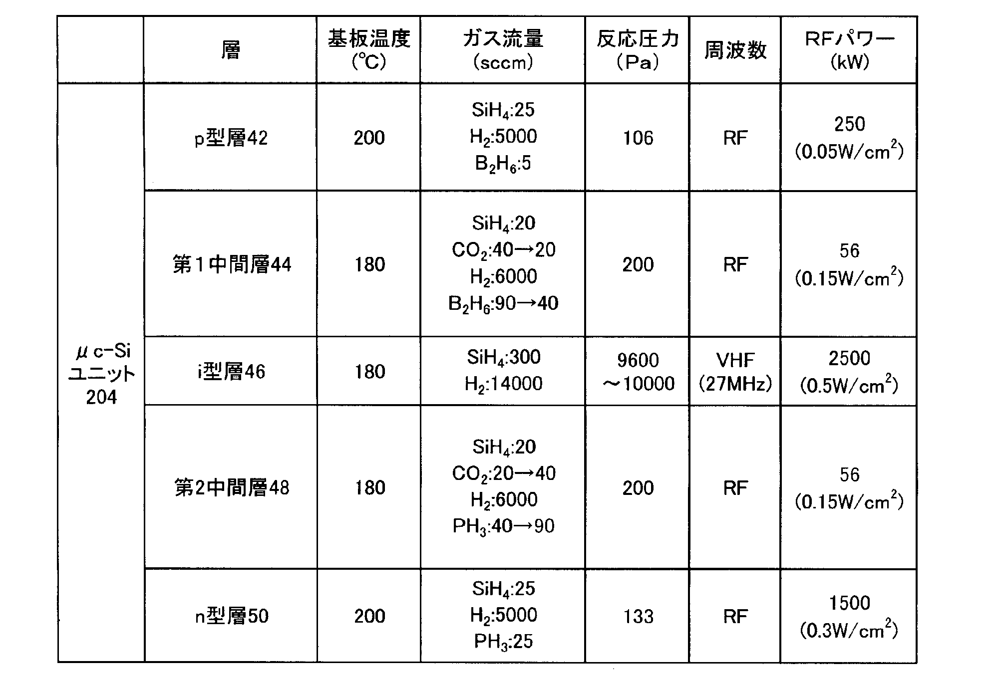
プラズマCVD法は、a-Siユニット202と同様に、例えば、13.56MHzのRFプラズマCVD法を適用することが好適である。一般的に、p型層42、i型層46及びn型層50はそれぞれ別の成膜室において成膜される。また、第1中間層44及び第2中間層48は、p型層36、n型層40、p型層42及びn型層50のいずれかの成膜室を用いて成膜してもよい。
p型層42は、a-Siユニット202のn型層40上に形成される。p型層42は、微結晶シリコン層若しくはアモルファスシリコン層又はそれらの組み合わせとすることが好適である。p型層42の膜質は、シリコン含有ガス、炭化水素ガス、p型ドーパント含有ガス及び希釈ガスの混合比、圧力及びプラズマ発生用高周波パワーを調整することによって変化させることができる。
第1中間層44は、p型層40上に形成される。第1中間層44は、後述する第2中間層48と共に、μc-Siユニット204の発電層であるi型層46に光を閉じ込める役割を果たす。第1中間層44は、p型ドーパント(ボロン等)をドープした酸化シリコンを含む層とすることが好適である。例えば、第1中間層44は、シリコン含有ガス、p型ドーパント含有ガス及び希釈ガスに二酸化炭素(CO2)等の酸素含有ガスを混合した混合ガスを用いてプラズマCVD法により形成することが好適である。第1中間層44の膜質は、添加ガス種、ガスの混合比、圧力及びプラズマ発生用高周波パワーを調整することによって変化させることができる。
図2は、本実施の形態における光電変換装置200の各層の屈折率を示す。図2に示すように、第1中間層44の屈折率n1は、光閉じ込めの対象となるμc-Siユニット204のi型層46の屈折率niよりも小さくする。また、第1中間層44の屈折率n1は、隣接するp型層42の屈折率np以下とする。さらに、本実施の形態では、第1中間層44の屈折率を膜厚方向に変化させたものとする。第1中間層44は、図2に示すように、i型層46側からp型層42側に向けて徐々に屈折率n1が大きくなるように形成される。
第1中間層44の屈折率n1は、p型層42との界面においてp型層42の屈折率npと略等しくなるようにすることが好適である。具体的には、p型層42の屈折率npは3.6程度であるので、p型層42との界面において第1中間層44の屈折率n1は3.6程度になるようにすることが好適である。また、第1中間層44の屈折率n1は、i型層46との界面において膜質が低下しない程度にできるだけ小さくすることが好適である。具体的には、i型層46との界面において第1中間層44の屈折率n1は2.1程度にすることが好適である。
第1中間層44の屈折率n1を膜厚方向で変化させるためには、成膜中において、シリコン含有ガス、ドーパント含有ガス、希釈ガスの混合ガスに対する二酸化炭素(CO2)等の酸素含有ガスの混合比を連続的に変化させればよい。すなわち、屈折率n1をより低下させるには二酸化炭素(CO2)等の酸素含有ガスの混合比をより高くなるように調整すればよい。また、第1中間層44のプラズマCVD法による成膜時の圧力及びプラズマ発生用高周波パワー等の成膜条件を調整しても第1中間層44の屈折率n1を変化させることができる。
第1中間層44上にはi型層46が形成される。i型層46は、ドープされていない膜厚0.5μm以上5μm以下の微結晶シリコン膜とする。i型層46は、μc-Siユニット204の発電層となる層である。i型層46は、まずバッファ層を形成し、バッファ層上に主発電層を形成した積層構造とすることが好適である。バッファ層は、主発電層の成膜条件よりも高い結晶化率となる成膜条件で成膜する。すなわち、ガラス基板等に単膜として成膜したときにバッファ層は主発電層よりも結晶化率が高くなる成膜条件で形成する。i型層46の膜質は、シリコン含有ガス及び希釈ガスの混合比、圧力及びプラズマ発生用高周波パワーを調整することによって変化させることができる。
第2中間層48は、i型層46上に形成される。第2中間層48は、n型ドーパント(リン等)をドープした酸化シリコンを含む層とすることが好適である。例えば、第2中間層48は、シリコン含有ガス、n型ドーパント含有ガス及び希釈ガスに二酸化炭素(CO2)等の酸素含有ガスを混合した混合ガスを用いてプラズマCVD法により形成することが好適である。第2中間層48の膜質は、添加ガス種、ガスの混合比、圧力及びプラズマ発生用高周波パワーを調整することによって変化させることができる。
図2に示すように、第2中間層48の屈折率n2は、光閉じ込めの対象となるμc-Siユニット204のi型層46の屈折率niよりも小さくする。また、第2中間層48の屈折率n2は、隣接するn型層50の屈折率nn以下とする。さらに、本実施の形態では、第2中間層48は、その屈折率n2が膜厚方向に沿って変化するように形成される。第2中間層48は、図2に示すように、i型層46側からn型層50側に向けて徐々に屈折率n2が大きくなるように形成される。
第2中間層48の屈折率n2は、n型層50との界面においてn型層50の屈折率nnと略等しくなるようにすることが好適である。具体的には、n型層50の屈折率nnは3.6程度であるので、n型層50との界面において第2中間層48の屈折率n2は3.6程度になるようにすることが好適である。また、第2中間層48の屈折率n2は、i型層46との界面において膜質が低下しない程度にできるだけ小さくすることが好適である。具体的には、i型層46との界面において第2中間層48の屈折率n2は2.1程度にすることが好適である。
第2中間層48の屈折率n2を膜厚方向で変化させるためには、成膜中において、シリコン含有ガス、ドーパント含有ガス、希釈ガスの混合ガスに対する二酸化炭素(CO2)等の酸素含有ガスの混合比を連続的に変化させればよい。すなわち、屈折率n2をより低下させるには二酸化炭素(CO2)等の酸素含有ガスの混合比をより高くなるように調整すればよい。また、第2中間層48のプラズマCVD法による成膜時の圧力及びプラズマ発生用高周波パワー等の成膜条件を調整しても第2中間層48の屈折率n2を変化させることができる。
n型層50は、第2中間層48上に形成される。n型層50は、n型ドーパント(リン等)をドープした膜厚5nm以上50nm以下n型微結晶シリコン層(n型μc-Si:H)とする。n型層50の膜質は、シリコン含有ガス、炭化水素ガス、n型ドーパント含有ガス及び希釈ガスの混合比、圧力及びプラズマ発生用高周波パワーを調整することによって変化させることができる。
ただし、本実施の形態においてμc-Siユニット204はこれに限定されるものではなく、発電層となるi型層46にi型微結晶シリコン層(i型μc-Si:H)が用いられ、i型層46を挟み込むように第1中間層44及び第2中間層48を備えるものであればよい。
μc-Siユニット204上に、裏面電極層34が形成される。裏面電極層34は、反射性金属と透明導電性酸化物(TCO)との積層構造をすることが好適である。透明導電性酸化物(TCO)としては、酸化錫(SnO2)、酸化亜鉛(ZnO)、インジウム錫酸化物(ITO)等、又は、これらに不純物をドープしたものが用いられる。例えば、酸化亜鉛(ZnO)にアルミニウム(Al)を不純物としてドープしたものでもよい。また、反射性金属としては、銀(Ag)、アルミニウム(Al)等の金属が用いられる。透明導電性酸化物(TCO)及び反射性金属は、例えば、スパッタリング法又はCVD法等により形成することができる。透明導電性酸化物(TCO)と反射性金属の少なくとも一方には、光閉じ込め効果を高めるための凹凸が設けることが好適である。
さらに、裏面電極層34を保護膜(図示しない)で被ってもよい。保護膜は、EVA、ポリイミド等の樹脂材料とし、同様の樹脂材料である充填材により裏面電極層34上を被うように接着すればよい。これによって、光電変換装置200の発電層への水分の侵入等を防ぐことができる。
なお、YAGレーザ(基本波1064nm、2倍高調波532nm)を用いて、透明導電層32、a-Siユニット202、μc-Siユニット204、裏面電極層34の分離加工を行うことによって、複数のセルを直列に接続した構成にしてもよい。
以下、第1中間層44及び第2中間層48の作用について説明する。図2の矢印(実線)で示すように、p型層42と第1中間層44との界面を透過してi型層46に入射した光は、i型層46と第2中間層48との界面において互いの屈折率差によって反射されてi型層46へ戻される。さらに、i型層46と第2中間層48との界面において反射された光は、i型層46と第1中間層44との界面に到達すると互いの屈折率差によって再び反射されi型層46へ戻される。このようにして、第1中間層44及び第2中間層48によって、ボトムセルとなるμc-Siユニット204のi型層46への光閉じ込め効果が得られる。
また、図2の矢印(破線)で示すように、i型層46と第2中間層48との界面では一部の光が透過するが、その光は、n型層50を通って、n型層50と裏面電極層34とに到達し、n型層50と裏面電極層34との屈折率差によって反射されてn型層50及び第2中間層48を通って再びi型層46へ戻される。そして、上記と同様に、裏面電極層34で反射された光も第1中間層44と第2中間層48とによってi型層46へ閉じ込められる。
ここで、屈折率n1に傾斜を設けることによって、p型層42と第1中間層44との界面の屈折率差(np-n1)はi型層46と第1中間層44との界面の屈折率差(ni-n1)より小さくなり、p型層42側から入射してくる光に対しては光の透過率をより向上させることができる。一方、i型層46に一旦入射した光がn型層50と裏面電極層34との間等のいずれかの場所で反射してi型層46と第1中間層44との界面に到達した場合、i型層46と第1中間層44との界面の屈折率差(ni-n1)によって、i型層46への反射率を高めることができる。
また、屈折率n2に傾斜を設けることによって、n型層50と第2中間層48との界面の屈折率差(nn-n2)はi型層46と第2中間層48との界面の屈折率差(ni-n2)より小さくなり、裏面電極層34等で反射してn型層50側から入射してくる光に対しては光の透過率を向上させることができる。一方、i型層46に一旦入射した光がi型層46と第2中間層48との界面に到達した場合、i型層46と第2中間層48との界面の屈折率差(ni-n2)によって、i型層46への反射率を高めることができる。
このようにして、ボトムセルとなるμc-Siユニット204のi型層46での光の利用効率を高めることができる。
ここで、p型層42との界面における第1中間層44の屈折率n1はn型層50との界面における第2中間層48の屈折率n2よりも大きくすることが好適である。p型層42の屈折率npとn型層50の屈折率nnとは同程度の大きさであるので、p型層42と第1中間層44との界面では、n型層50と第2中間層48との界面よりもi型層46への光の導入率を高めることができる。
また、第1中間層44の膜厚d1は第2中間層48の膜厚d2以下とすることが好適である。これにより、第1中間層44とi型層46との界面における反射率はi型層46と第2中間層48との界面における反射率よりも多少低下するが、透明絶縁基板30からの光入射側である第1中間層44における光の吸収が抑制され、i型層46へ到達する光量を増加させることができ、光電変換装置200全体としての発電効率を高めることができる。一方、第2中間層48における光の吸収量は第1中間層44における光の吸収量よりも大きくなるが、裏面電極層34から反射されて第2中間層48へ入射してくる光は透明絶縁基板30側から第1中間層44へ入射してくる光よりも小さく、i型層46と第2中間層48との界面における反射率をより高めることによって、i型層46への光閉じ込め効果が高まり、光電変換装置200全体としての発電効率を高めることができる。
具体的には、第1中間層44及び第2中間層48の膜厚d1,d2は、30nm以上100nm以下とすることが好適である。特に、第1中間層44の膜厚d1は、30nm以上50nm以下の範囲とし、第2中間層48の膜厚d2は、第1中間層44の膜厚d1以上であって50nm以上100nm以下の範囲とすることが好適である。
また、第1中間層44及び第2中間層48の屈折率n1,n2は、膜厚方向に連続的に傾斜させることに限定されるものではなく、図3に示すように、階段状に変化させてもよい。
各層の屈折率は、光電変換装置200の断面に対してエネルギー分散型X線分析(EDX)による成分分析を行うことで知ることができる。EDXによる成分分析において、着目する断面領域の酸素(O)の含有量が他の断面領域よりも高い場合、着目する断面領域は当該他の断面領域よりも屈折率が低いと判定できる。例えば、μc-Siユニット204のi型層46の両側にi型層46よりも酸素(O)の酸素含有量が多い層が設けられていれば本実施の形態における光電変換装置200の構成を有するものと判定できる。また、第1中間層44及び第2中間層48とp型層42及びn型層50との屈折率の関係も同様に判定できる。
各層の屈折率の関係については、後述する他の実施の形態及び変形例においても同様に判定することができる。
なお、本実施の形態では第1中間層44及び第2中間層48として不純物をドープした酸化シリコンを含む層を適用したが、これに限定されるものではない。例えば、第1中間層44及び第2中間層48は、酸化亜鉛(ZnO)等の透明導電性酸化物(TCO)としてもよい。特に、マグネシウム(Mg)がドープされた酸化亜鉛(ZnO)を用いることが好適である。透明導電性酸化物(TCO)は、例えば、スパッタリング法やCVD法等により形成することができる。
<第2の実施の形態>
第2の実施の形態における光電変換装置206は、図4に示すように、第1の実施の形態における光電変換装置200の第1中間層44のみを設けて、第2中間層48を設けない構成とする。
第2の実施の形態における光電変換装置206は、図4に示すように、第1の実施の形態における光電変換装置200の第1中間層44のみを設けて、第2中間層48を設けない構成とする。
この場合、第1中間層44の働きは、第1の実施の形態における光電変換装置200と同様である。一方、第2中間層48が設けられていないので、p型層42と第1中間層44との界面を透過してi型層46に入射した光は、n型層50と裏面電極層34との界面において反射されてi型層46へ戻される。その反射された光は、i型層46と第1中間層44との界面に到達すると互いの屈折率差によって再び反射されi型層46へ戻される。このようにして、第1中間層44及び裏面電極層34によって、ボトムセルとなるμc-Siユニット204のi型層46への光閉じ込め効果が得られる。
なお、第1中間層44を設けず、第2中間層48のみを設ける構成としてもよい。この場合、第2中間層48の働きは、第1の実施の形態における光電変換装置200と同様である。第1中間層44が設けられていないので、i型層46に対する光閉じ込め効果は低減するが、第2中間層48による反射の効果は得られる。
<第3の実施の形態>
図5は、第3の実施の形態における光電変換装置300の構造を示す断面図である。本実施の形態における光電変換装置300は、第1の実施の形態における光電変換装置200のようにμc-Siユニット204に第1中間層44及び第2中間層48を設ける代りに、a-Siユニット202に第1中間層52及び第2中間層54を設けている。各層の成膜方法は、第1の実施の形態と同様であるので説明を省略する。
図5は、第3の実施の形態における光電変換装置300の構造を示す断面図である。本実施の形態における光電変換装置300は、第1の実施の形態における光電変換装置200のようにμc-Siユニット204に第1中間層44及び第2中間層48を設ける代りに、a-Siユニット202に第1中間層52及び第2中間層54を設けている。各層の成膜方法は、第1の実施の形態と同様であるので説明を省略する。
図6は、本実施の形態における光電変換装置300の各層の屈折率を示す。図6に示すように、第1中間層52の屈折率n1及び第2中間層54の屈折率n2は、光閉じ込めの対象となるa-Siユニット202のi型層38の屈折率naiよりも小さくする。また、第1中間層52の屈折率n1は、隣接するp型層36の屈折率nap以下とする。また、第2中間層54の屈折率n2は、隣接するn型層40の屈折率nan以下とする。
さらに、本実施の形態では、第1中間層52の屈折率を膜厚方向に変化させたものとする。第1中間層52は、図6に示すように、i型層38側からp型層36側に向けて徐々に屈折率n1が大きくなるように形成される。さらに、第2中間層54は、その屈折率n2が膜厚方向に沿って変化するように形成される。第2中間層54は、図6に示すように、i型層38側からn型層40側に向けて徐々に屈折率n2が大きくなるように形成される。
第1中間層52の屈折率n1は、p型層36との界面においてp型層36の屈折率napと略等しくなるようにすることが好適である。具体的には、p型層36の屈折率napは3.6程度であるので、p型層36との界面において第1中間層52の屈折率n1は3.6程度になるようにすることが好適である。また、第1中間層52の屈折率n1は、i型層38との界面において膜質が低下しない程度にできるだけ小さくすることが好適である。具体的には、i型層38との界面において第1中間層52の屈折率n1は2.1程度にすることが好適である。
第2中間層54の屈折率n2は、n型層40との界面においてn型層40の屈折率nanと略等しくなるようにすることが好適である。具体的には、n型層40の屈折率nanは3.6程度であるので、n型層40との界面において第2中間層54の屈折率n2は3.6程度になるようにすることが好適である。また、第2中間層54の屈折率n2は、i型層38との界面において膜質が低下しない程度にできるだけ小さくすることが好適である。具体的には、i型層38との界面において第2中間層54の屈折率n2は2.1程度にすることが好適である。
以下、第1中間層52及び第2中間層54の作用について説明する。図6の矢印(実線)で示すように、p型層36と第1中間層52との界面を透過してi型層38に入射した光は、i型層38と第2中間層54との界面において互いの屈折率差によって反射されてi型層38へ戻される。さらに、i型層38と第2中間層54との界面において反射された光は、i型層38と第1中間層52との界面に到達すると互いの屈折率差によって再び反射されi型層38へ戻される。このようにして、第1中間層52及び第2中間層54によって、トップセルとなるa-Siユニット202のi型層38への光閉じ込め効果が得られる。
また、図6の矢印(破線)で示すように、i型層38と第2中間層54との界面では一部の光が透過するが、その光は、n型層40、p型層42、i型層46、n型層50を通って、n型層50と裏面電極層34とに到達し、n型層50と裏面電極層34との屈折率差によって反射されて再びi型層38へ戻される。そして、上記と同様に、裏面電極層34で反射された光も第1中間層52と第2中間層54とによってi型層38へ閉じ込められる。
ここで、屈折率n1に傾斜を設けることによって、p型層36と第1中間層52との界面の屈折率差(nap-n1)はi型層38と第1中間層52との界面の屈折率差(nai-n1)より小さくなり、p型層36側から入射してくる光に対しては光の透過率をより向上させることができる。一方、i型層38に一旦入射した光が第2中間層54とn型層40との界面等で反射してi型層38と第1中間層52との界面に到達した場合、i型層38と第1中間層52との界面の屈折率差(nai-n1)によって、i型層38への反射率を高めることができる。
また、屈折率n2に傾斜を設けることによって、n型層40と第2中間層54との界面の屈折率差(nan-n2)はi型層38と第2中間層54との界面の屈折率差(nai-n2)より小さくなり、裏面電極層34等で反射してn型層40側から入射してくる光に対しては光の透過率を向上させることができる。一方、i型層38に一旦入射した光がi型層38と第2中間層54との界面に到達した場合、i型層38と第2中間層54との界面の屈折率差(nai-n2)によって、i型層46への反射率を高めることができる。
このようにして、トップセルとなるa-Siユニット202のi型層38での光の利用効率を高めることができる。
ここで、p型層36との界面における第1中間層52の屈折率n1はn型層40との界面における第2中間層54の屈折率n2よりも大きくすることが好適である。p型層36の屈折率napとn型層40の屈折率nanとは同程度の大きさであるので、p型層36と第1中間層52との界面では、n型層40と第2中間層54との界面よりもi型層38への光の導入率を高めることができる。
また、第1中間層52の膜厚d1は第2中間層54の膜厚d2以下とすることが好適である。これにより、第1中間層52とi型層38との界面における反射率はi型層38と第2中間層54との界面における反射率よりも多少低下するが、透明絶縁基板30からの光入射側である第1中間層52における光の吸収が抑制され、i型層38へ到達する光量を増加させることができ、光電変換装置300全体としての発電効率を高めることができる。一方、第2中間層54における光の吸収量は第1中間層52における光の吸収量よりも大きくなるが、反射されて第2中間層54へ入射してくる光は透明絶縁基板30側から第1中間層52へ入射してくる光よりも小さく、i型層38と第2中間層54との界面における反射率をより高めることによって、i型層38への光閉じ込め効果が高まり、光電変換装置300全体としての発電効率を高めることができる。
具体的には、第1中間層52及び第2中間層54の膜厚d1,d2は、30nm以上100nm以下とすることが好適である。特に、第1中間層52の膜厚d1は、30nm以上50nm以下の範囲とし、第2中間層54の膜厚d2は、第1中間層52の膜厚d1以上であって50nm以上100nm以下の範囲とすることが好適である。
また、第1中間層52及び第2中間層54の屈折率n1,n2は、膜厚方向に連続的に傾斜させることに限定されるものではなく、図7に示すように、階段状に変化させてもよい。
なお、本実施の形態では第1中間層52及び第2中間層54として不純物をドープした酸化シリコンを含む層を適用したが、これに限定されるものではない。例えば、第1中間層52及び第2中間層54は、酸化亜鉛(ZnO)等の透明導電性酸化物(TCO)としてもよい。特に、マグネシウム(Mg)がドープされた酸化亜鉛(ZnO)を用いることが好適である。透明導電性酸化物(TCO)は、例えば、スパッタリング法やCVD法等により形成することができる。
<第4の実施の形態>
第4の実施の形態における光電変換装置302は、図8に示すように、第3の実施の形態における光電変換装置300の第2中間層54のみを設けて、第1中間層52を設けない構成とする。
第4の実施の形態における光電変換装置302は、図8に示すように、第3の実施の形態における光電変換装置300の第2中間層54のみを設けて、第1中間層52を設けない構成とする。
この場合、第2中間層54の働きは、第3の実施の形態における光電変換装置300と同様である。第2中間層54を設けることによりi型層38への光の反射を高めることができ、トップセルとなるa-Siユニット202での発電効率を高めることができる。
なお、第2中間層54を設けず、第1中間層52のみを設ける構成としてもよい。この場合、第1中間層52の働きは、第3の実施の形態における光電変換装置300と同様である。一方、第2中間層54が設けられていないので、i型層38で吸収されなかった光は、n型層40、ボトムセルとなるμc-Siユニット204を通って裏面電極層34まで到達して反射され、さらにボトムセルとなるμc-Siユニット204で吸収されなかったときにi型層38へ戻される。その反射された光は、i型層38と第1中間層52との界面に到達すると互いの屈折率差によって再び反射されi型層38へ戻される。このようにして、第1中間層52及び裏面電極層34によって、トップセルとなるa-Siユニット202及びボトムセルとなるμc-Siユニット204への光閉じ込め効果が得られる。
さらに、第1~第4の実施の形態における構成を適宜組み合わせた構成としてもよい。これにより、それぞれにおける光閉じ込め等の効果を相乗的に得ることができ、光電変換装置の発電効率をより高めることができる。
<第5の実施の形態>
本願発明は、結晶系の光電変換装置に対して適用することができる。図9は、単結晶シリコン層60を備える光電変換装置400の構造を示す断面模式図である。
本願発明は、結晶系の光電変換装置に対して適用することができる。図9は、単結晶シリコン層60を備える光電変換装置400の構造を示す断面模式図である。
光電変換装置400は、単結晶シリコン層60の表面(第1面)に第1中間層62、真性半導体層64及び導電型半導体層66を順次形成し、単結晶シリコン層60の裏面(第2面)に第2中間層68、真性半導体層70及び導電型半導体層72を形成した構造を有する。
単結晶シリコン層60は、n型の単結晶シリコン(抵抗率=約0.5~4Ωcm)とすることが好適である。例えば、単結晶シリコン層60は、100mm角の正方形で、厚さ約100~500μmとすることが好適である。
単結晶シリコン層60の表面(第1面)には第1中間層62を形成する。第1中間層62は、第1の実施の形態における第1中間層44と同様に形成することができる。第1中間層62上にはプラズマCVD法を用いてドープされていないアモルファスシリコン層である真性半導体層64(膜厚:約50~200Å)及びp型ドーパントが添加されたp型アモルファスシリコン層である導電型半導体層66(膜厚:約50~150Å)を形成する。なお、真性半導体層64及び導電型半導体層66は、アモルファスシリコンとしたが、微結晶シリコンを用いてもよい。
単結晶シリコン層60の裏面(第2面)には第2中間層68を形成する。第2中間層68は、第1の実施の形態における第2中間層48と同様に形成することができる。第2中間層68上にはプラズマCVD法を用いてドープされていないアモルファスシリコン層である真性半導体層70(膜厚:約50~200Å)及びn型ドーパントが添加されたn型アモルファスシリコン層である導電型半導体層72(膜厚:約100~500Å)を形成する。なお、真性半導体層70及び導電型半導体層72は、アモルファスシリコンとしたが、微結晶シリコンを用いてもよい。
導電型半導体層66及び72上には、これらと略同面積の透明導電層74及び76を形成する。さらに、透明導電層74及び76の上に、銀ペースト等からなる集電極78及び80を形成する。なお、光電変換装置400では、裏面(第2面)側においても透明導電層76を採用しているので、裏面側に光が入射しても発電に寄与する。
図10は、光電変換装置400の各層の屈折率を示す。図10に示すように、第1中間層62の屈折率n1及び第2中間層68の屈折率n2は、光閉じ込めの対象となる単結晶シリコン層60の屈折率nciよりも小さくする。また、第1中間層62の屈折率n1は、隣接する真性半導体層64及び導電型半導体層66の屈折率npi以下とする。さらに、本実施の形態では、第1中間層62の屈折率n1を膜厚方向に変化させたものとする。第1中間層62は、図10に示すように、単結晶シリコン層60側から真性半導体層64側に向けて徐々に屈折率n1が大きくなるように形成される。
また、第2中間層68の屈折率n2は、隣接する真性半導体層70及び導電型半導体層72の屈折率nni以下とする。さらに、本実施の形態では、第2中間層68の屈折率n2を膜厚方向に変化させたものとする。第2中間層68は、単結晶シリコン層60側から真性半導体層70側に向けて徐々に屈折率n2が大きくなるように形成される。
これにより、図10の矢印(実線)で示すように、真性半導体層64と第1中間層62との界面を透過して単結晶シリコン層60に入射した光は、単結晶シリコン層60と第2中間層68との界面において互いの屈折率差によって反射されて単結晶シリコン層60へ戻される。さらに、単結晶シリコン層60と第2中間層68との界面において反射された光は、単結晶シリコン層60と第1中間層62との界面に到達すると互いの屈折率差によって再び反射され単結晶シリコン層60へ戻される。また、図10の矢印(破線)で示すように、真性半導体層70と第2中間層68との界面を透過して単結晶シリコン層60に入射した光は、単結晶シリコン層60と第1中間層62との界面において互いの屈折率差によって反射されて単結晶シリコン層60へ戻される。さらに、単結晶シリコン層60と第2中間層68との界面に到達すると互いの屈折率差によって再び反射され単結晶シリコン層60へ戻される。このようにして、第1中間層62及び第2中間層68によって、単結晶シリコン層60への光閉じ込め効果が得られる。
ここで、屈折率n1に傾斜を設けることによって、真性半導体層64と第1中間層62との界面の屈折率差(npi-n1)は単結晶シリコン層60と第1中間層62との界面の屈折率差(nci-n1)より小さくなり、真性半導体層64側から入射してくる光に対しては光の透過率をより向上させることができる。一方、単結晶シリコン層60に一旦入射した光が真性半導体層70と裏面電極層76との間等のいずれかの場所で反射して単結晶シリコン層60と第1中間層62との界面に到達した場合、単結晶シリコン層60と第1中間層62との界面の屈折率差(nci-n1)によって、単結晶シリコン層60への反射率を高めることができる。
また、屈折率n2に傾斜を設けることによって、真性半導体層70と第2中間層68との界面の屈折率差(nni-n2)は単結晶シリコン層60と第2中間層68との界面の屈折率差(nci-n2)より小さくなり、真性半導体層70側から入射してくる光に対しては光の透過率を向上させることができる。一方、単結晶シリコン層60に一旦入射した光が単結晶シリコン層60と第2中間層68との界面に到達した場合、単結晶シリコン層60と第2中間層68との界面の屈折率差(nci-n2)によって、単結晶シリコン層60への反射率を高めることができる。
以上のように、第1中間層62及び第2中間層68を設けることによって、単結晶シリコン層60への光閉じ込め効果を得ることができ、光の利用効率を高めることができる。
なお、第1中間層62の屈折率n1は、真性半導体層64との界面において真性半導体層64の屈折率npiと略等しくなるようにすることが好適である。第2中間層68の屈折率n2は、真性半導体層70との界面において真性半導体層70の屈折率nniと略等しくなるようにすることが好適である。また、第1中間層62の屈折率n1及び第2中間層68の屈折率n2は、単結晶シリコン層60との界面において膜質が低下しない程度にできるだけ小さくすることが好適である。
また、第1中間層62の膜厚d1は第2中間層68の膜厚d2以下とすることが好適である。これにより、第1中間層62と単結晶シリコン層60との界面における反射率は単結晶シリコン層60と第2中間層68との界面における反射率よりも多少低下するが、主な光の入射側に配置される第1中間層62における光の吸収が抑制され、単結晶シリコン層60へ到達する光量を増加させることができ、光電変換装置400全体としての発電効率を高めることができる。一方、第2中間層68における光の吸収量は第1中間層62における光の吸収量よりも大きくなるが、第2中間層68を透過して単結晶シリコン層60へ到達する光は第1中間層62を透過して単結晶シリコン層60へ到達する光よりも小さく、単結晶シリコン層60と第2中間層68との界面における反射率をより高めることによって、単結晶シリコン層60への光閉じ込め効果が高まり、光電変換装置400全体としての発電効率を高めることができる。
また、第1中間層62及び第2中間層68の屈折率n1,n2は、膜厚方向に連続的に傾斜させることに限定されるものではなく、図11に示すように、階段状に変化させてもよい。
第1中間層62及び第2中間層68は少なくとも一方を設けることによって光電変換装置の発電効率を向上させる効果を奏することができる。また、発電層である単結晶シリコン層60を2層以上積層した光電変換装置においても単結晶シリコン層60毎に第1中間層62又は第2中間層68を設けることによって光閉じ込め効果を得ることができる。
10 基板、12 透明導電層、14 アモルファスシリコン光電変換ユニット(a-Siユニット)、16 微結晶シリコン光電変換ユニット(μc-Siユニット)、20 中間層、30 透明絶縁基板、32 透明導電層、34 裏面電極層、36 p型層(a-Si)、38 i型層(a-Si)、40 n型層(a-Si)、42 p型層(μc-Si)、44,56,62 第1中間層、46 i型層(μc-Si)、48,58,68 第2中間層、50 n型層(μc-Si)、60 単結晶シリコン層、64 真性半導体層、66 導電型半導体層、70 真性半導体層、72 導電型半導体層、74,76 透明導電層、78,80 集電極、100,200,206,300,302,400 光電変換装置、202 アモルファスシリコン光電変換ユニット(a-Siユニット)、204 微結晶シリコン光電変換ユニット(μc-Siユニット)。
Claims (4)
- p型層、i型層、n型層である半導体膜を積層した光電変換装置であって、
前記i型層に接し、前記i型層より小さい屈折率の範囲内において前記i型層に接する側から前記i型層に接しない側に向かって屈折率が大きくなる中間層を備えることを特徴とする光電変換装置。 - 請求項1に記載の光電変換装置であって、
前記中間層は、前記i型層を挟むように配置された第1中間層及び第2中間層を備えることを特徴とする光電変換装置。 - 請求項2に記載の光電変換装置であって、
前記第1中間層は、前記第2中間層より光入射面に近く配置され、
前記第2中間層の前記i型層に接する側の屈折率より前記第1中間層の前記i型層に接する側の屈折率が大きいことを特徴とする光電変換装置。 - 請求項2又は3に記載の光電変換装置であって、
前記第1中間層は、前記第2中間層より光入射面に近く配置され、前記第2中間層以下の膜厚であることを特徴とする光電変換装置。
Priority Applications (1)
| Application Number | Priority Date | Filing Date | Title |
|---|---|---|---|
| US13/614,788 US20130014810A1 (en) | 2010-04-28 | 2012-09-13 | Photoelectric conversion device |
Applications Claiming Priority (2)
| Application Number | Priority Date | Filing Date | Title |
|---|---|---|---|
| JP2010-104455 | 2010-04-28 | ||
| JP2010104455A JP4940328B2 (ja) | 2010-04-28 | 2010-04-28 | 光電変換装置 |
Related Child Applications (1)
| Application Number | Title | Priority Date | Filing Date |
|---|---|---|---|
| US13/614,788 Continuation US20130014810A1 (en) | 2010-04-28 | 2012-09-13 | Photoelectric conversion device |
Publications (1)
| Publication Number | Publication Date |
|---|---|
| WO2011136167A1 true WO2011136167A1 (ja) | 2011-11-03 |
Family
ID=44861466
Family Applications (1)
| Application Number | Title | Priority Date | Filing Date |
|---|---|---|---|
| PCT/JP2011/060043 Ceased WO2011136167A1 (ja) | 2010-04-28 | 2011-04-25 | 光電変換装置 |
Country Status (3)
| Country | Link |
|---|---|
| US (1) | US20130014810A1 (ja) |
| JP (1) | JP4940328B2 (ja) |
| WO (1) | WO2011136167A1 (ja) |
Cited By (1)
| Publication number | Priority date | Publication date | Assignee | Title |
|---|---|---|---|---|
| WO2013065538A1 (ja) * | 2011-11-03 | 2013-05-10 | 三洋電機株式会社 | 光電変換装置 |
Families Citing this family (2)
| Publication number | Priority date | Publication date | Assignee | Title |
|---|---|---|---|---|
| US8904876B2 (en) * | 2012-09-29 | 2014-12-09 | Stryker Corporation | Flexible piezocapacitive and piezoresistive force and pressure sensors |
| JP6306411B2 (ja) * | 2014-04-17 | 2018-04-04 | 株式会社日立国際電気 | 半導体装置の製造方法、基板処理装置およびプログラム |
Citations (2)
| Publication number | Priority date | Publication date | Assignee | Title |
|---|---|---|---|---|
| JP2009290115A (ja) * | 2008-05-30 | 2009-12-10 | Kaneka Corp | シリコン系薄膜太陽電池 |
| JP2010123944A (ja) * | 2008-11-21 | 2010-06-03 | Ind Technol Res Inst | 反射構造を有する太陽電池 |
Family Cites Families (1)
| Publication number | Priority date | Publication date | Assignee | Title |
|---|---|---|---|---|
| US8207010B2 (en) * | 2007-06-05 | 2012-06-26 | Semiconductor Energy Laboratory Co., Ltd. | Method for manufacturing photoelectric conversion device |
-
2010
- 2010-04-28 JP JP2010104455A patent/JP4940328B2/ja not_active Expired - Fee Related
-
2011
- 2011-04-25 WO PCT/JP2011/060043 patent/WO2011136167A1/ja not_active Ceased
-
2012
- 2012-09-13 US US13/614,788 patent/US20130014810A1/en not_active Abandoned
Patent Citations (2)
| Publication number | Priority date | Publication date | Assignee | Title |
|---|---|---|---|---|
| JP2009290115A (ja) * | 2008-05-30 | 2009-12-10 | Kaneka Corp | シリコン系薄膜太陽電池 |
| JP2010123944A (ja) * | 2008-11-21 | 2010-06-03 | Ind Technol Res Inst | 反射構造を有する太陽電池 |
Cited By (1)
| Publication number | Priority date | Publication date | Assignee | Title |
|---|---|---|---|---|
| WO2013065538A1 (ja) * | 2011-11-03 | 2013-05-10 | 三洋電機株式会社 | 光電変換装置 |
Also Published As
| Publication number | Publication date |
|---|---|
| JP4940328B2 (ja) | 2012-05-30 |
| US20130014810A1 (en) | 2013-01-17 |
| JP2011233786A (ja) | 2011-11-17 |
Similar Documents
| Publication | Publication Date | Title |
|---|---|---|
| JP2010283161A (ja) | 太陽電池及びその製造方法 | |
| WO2013002102A1 (ja) | 光電変換装置 | |
| WO2011065343A1 (ja) | 光電変換装置及びその製造方法 | |
| JP2016029675A (ja) | 薄膜太陽電池用透光性絶縁基板、及び集積型薄膜シリコン太陽電池 | |
| US8759667B2 (en) | Photoelectric conversion device | |
| JP5291633B2 (ja) | シリコン系薄膜光電変換装置およびその製造方法 | |
| JP4940328B2 (ja) | 光電変換装置 | |
| JP4940327B2 (ja) | 光電変換装置 | |
| JP4945686B2 (ja) | 光電変換装置 | |
| JP2011014619A (ja) | 太陽電池及びその製造方法 | |
| JP5420628B2 (ja) | 光電変換装置 | |
| JP2011014618A (ja) | 太陽電池及びその製造方法 | |
| JP2012060167A (ja) | 光電変換装置 | |
| WO2011105166A1 (ja) | 光電変換モジュール及びその製造方法 | |
| JP2010283162A (ja) | 太陽電池及びその製造方法 | |
| US20100307573A1 (en) | Solar cell and manufacturing method thereof | |
| JP2011216586A (ja) | 積層型光電変換装置および積層型光電変換装置の製造方法 | |
| WO2011148724A1 (ja) | 積層型光電変換装置用中間層、積層型光電変換装置および積層型光電変換装置の製造方法 | |
| JP2011077220A (ja) | 太陽電池 | |
| US8367453B2 (en) | Method of manufacturing solar battery | |
| JP2013026602A (ja) | 光電変換装置 | |
| US20100330266A1 (en) | Method of manufacturing solar battery | |
| JP2010283160A (ja) | 太陽電池及びその製造方法 | |
| JP2010283159A (ja) | 太陽電池及びその製造方法 | |
| WO2013065538A1 (ja) | 光電変換装置 |
Legal Events
| Date | Code | Title | Description |
|---|---|---|---|
| 121 | Ep: the epo has been informed by wipo that ep was designated in this application |
Ref document number: 11774948 Country of ref document: EP Kind code of ref document: A1 |
|
| NENP | Non-entry into the national phase |
Ref country code: DE |
|
| 122 | Ep: pct application non-entry in european phase |
Ref document number: 11774948 Country of ref document: EP Kind code of ref document: A1 |