WO2011132384A1 - 電子装置の製造方法および装置、その一対の挟圧部材 - Google Patents
電子装置の製造方法および装置、その一対の挟圧部材 Download PDFInfo
- Publication number
- WO2011132384A1 WO2011132384A1 PCT/JP2011/002184 JP2011002184W WO2011132384A1 WO 2011132384 A1 WO2011132384 A1 WO 2011132384A1 JP 2011002184 W JP2011002184 W JP 2011002184W WO 2011132384 A1 WO2011132384 A1 WO 2011132384A1
- Authority
- WO
- WIPO (PCT)
- Prior art keywords
- laminate
- terminal
- groove
- electronic component
- manufacturing
- Prior art date
- Legal status (The legal status is an assumption and is not a legal conclusion. Google has not performed a legal analysis and makes no representation as to the accuracy of the status listed.)
- Ceased
Links
Images




Classifications
-
- B—PERFORMING OPERATIONS; TRANSPORTING
- B23—MACHINE TOOLS; METAL-WORKING NOT OTHERWISE PROVIDED FOR
- B23K—SOLDERING OR UNSOLDERING; WELDING; CLADDING OR PLATING BY SOLDERING OR WELDING; CUTTING BY APPLYING HEAT LOCALLY, e.g. FLAME CUTTING; WORKING BY LASER BEAM
- B23K35/00—Rods, electrodes, materials, or media, for use in soldering, welding, or cutting
- B23K35/22—Rods, electrodes, materials, or media, for use in soldering, welding, or cutting characterised by the composition or nature of the material
- B23K35/36—Selection of non-metallic compositions, e.g. coatings or fluxes; Selection of soldering or welding materials, conjoint with selection of non-metallic compositions, both selections being of interest
- B23K35/3612—Selection of non-metallic compositions, e.g. coatings or fluxes; Selection of soldering or welding materials, conjoint with selection of non-metallic compositions, both selections being of interest with organic compounds as principal constituents
- B23K35/3613—Polymers, e.g. resins
-
- C—CHEMISTRY; METALLURGY
- C08—ORGANIC MACROMOLECULAR COMPOUNDS; THEIR PREPARATION OR CHEMICAL WORKING-UP; COMPOSITIONS BASED THEREON
- C08L—COMPOSITIONS OF MACROMOLECULAR COMPOUNDS
- C08L63/00—Compositions of epoxy resins; Compositions of derivatives of epoxy resins
-
- H—ELECTRICITY
- H05—ELECTRIC TECHNIQUES NOT OTHERWISE PROVIDED FOR
- H05K—PRINTED CIRCUITS; CASINGS OR CONSTRUCTIONAL DETAILS OF ELECTRIC APPARATUS; MANUFACTURE OF ASSEMBLAGES OF ELECTRICAL COMPONENTS
- H05K2201/00—Indexing scheme relating to printed circuits covered by H05K1/00
- H05K2201/02—Fillers; Particles; Fibers; Reinforcement materials
- H05K2201/0203—Fillers and particles
- H05K2201/0206—Materials
- H05K2201/0209—Inorganic, non-metallic particles
-
- H—ELECTRICITY
- H05—ELECTRIC TECHNIQUES NOT OTHERWISE PROVIDED FOR
- H05K—PRINTED CIRCUITS; CASINGS OR CONSTRUCTIONAL DETAILS OF ELECTRIC APPARATUS; MANUFACTURE OF ASSEMBLAGES OF ELECTRICAL COMPONENTS
- H05K2201/00—Indexing scheme relating to printed circuits covered by H05K1/00
- H05K2201/10—Details of components or other objects attached to or integrated in a printed circuit board
- H05K2201/10613—Details of electrical connections of non-printed components, e.g. special leads
- H05K2201/10954—Other details of electrical connections
- H05K2201/10977—Encapsulated connections
-
- H—ELECTRICITY
- H05—ELECTRIC TECHNIQUES NOT OTHERWISE PROVIDED FOR
- H05K—PRINTED CIRCUITS; CASINGS OR CONSTRUCTIONAL DETAILS OF ELECTRIC APPARATUS; MANUFACTURE OF ASSEMBLAGES OF ELECTRICAL COMPONENTS
- H05K3/00—Apparatus or processes for manufacturing printed circuits
- H05K3/30—Assembling printed circuits with electric components, e.g. with resistors
- H05K3/303—Assembling printed circuits with electric components, e.g. with resistors with surface mounted components
- H05K3/305—Affixing by adhesive
-
- H—ELECTRICITY
- H05—ELECTRIC TECHNIQUES NOT OTHERWISE PROVIDED FOR
- H05K—PRINTED CIRCUITS; CASINGS OR CONSTRUCTIONAL DETAILS OF ELECTRIC APPARATUS; MANUFACTURE OF ASSEMBLAGES OF ELECTRICAL COMPONENTS
- H05K3/00—Apparatus or processes for manufacturing printed circuits
- H05K3/30—Assembling printed circuits with electric components, e.g. with resistors
- H05K3/32—Assembling printed circuits with electric components, e.g. with resistors electrically connecting electric components or wires to printed circuits
- H05K3/34—Assembling printed circuits with electric components, e.g. with resistors electrically connecting electric components or wires to printed circuits by soldering
- H05K3/341—Surface mounted components
- H05K3/3431—Leadless components
- H05K3/3436—Leadless components having an array of bottom contacts, e.g. pad grid array or ball grid array components
-
- H—ELECTRICITY
- H10—SEMICONDUCTOR DEVICES; ELECTRIC SOLID-STATE DEVICES NOT OTHERWISE PROVIDED FOR
- H10W—GENERIC PACKAGES, INTERCONNECTIONS, CONNECTORS OR OTHER CONSTRUCTIONAL DETAILS OF DEVICES COVERED BY CLASS H10
- H10W72/00—Interconnections or connectors in packages
- H10W72/01—Manufacture or treatment
- H10W72/016—Manufacture or treatment of strap connectors
-
- H—ELECTRICITY
- H10—SEMICONDUCTOR DEVICES; ELECTRIC SOLID-STATE DEVICES NOT OTHERWISE PROVIDED FOR
- H10W—GENERIC PACKAGES, INTERCONNECTIONS, CONNECTORS OR OTHER CONSTRUCTIONAL DETAILS OF DEVICES COVERED BY CLASS H10
- H10W72/00—Interconnections or connectors in packages
- H10W72/071—Connecting or disconnecting
- H10W72/0711—Apparatus therefor
-
- H—ELECTRICITY
- H10—SEMICONDUCTOR DEVICES; ELECTRIC SOLID-STATE DEVICES NOT OTHERWISE PROVIDED FOR
- H10W—GENERIC PACKAGES, INTERCONNECTIONS, CONNECTORS OR OTHER CONSTRUCTIONAL DETAILS OF DEVICES COVERED BY CLASS H10
- H10W72/00—Interconnections or connectors in packages
- H10W72/071—Connecting or disconnecting
- H10W72/0711—Apparatus therefor
- H10W72/07125—Means for controlling the bonding environment, e.g. valves or vacuum pumps
-
- H—ELECTRICITY
- H10—SEMICONDUCTOR DEVICES; ELECTRIC SOLID-STATE DEVICES NOT OTHERWISE PROVIDED FOR
- H10W—GENERIC PACKAGES, INTERCONNECTIONS, CONNECTORS OR OTHER CONSTRUCTIONAL DETAILS OF DEVICES COVERED BY CLASS H10
- H10W72/00—Interconnections or connectors in packages
- H10W72/071—Connecting or disconnecting
- H10W72/0711—Apparatus therefor
- H10W72/07141—Means for applying energy, e.g. ovens or lasers
-
- H—ELECTRICITY
- H10—SEMICONDUCTOR DEVICES; ELECTRIC SOLID-STATE DEVICES NOT OTHERWISE PROVIDED FOR
- H10W—GENERIC PACKAGES, INTERCONNECTIONS, CONNECTORS OR OTHER CONSTRUCTIONAL DETAILS OF DEVICES COVERED BY CLASS H10
- H10W72/00—Interconnections or connectors in packages
- H10W72/071—Connecting or disconnecting
- H10W72/0711—Apparatus therefor
- H10W72/07188—Apparatus chuck
-
- H—ELECTRICITY
- H10—SEMICONDUCTOR DEVICES; ELECTRIC SOLID-STATE DEVICES NOT OTHERWISE PROVIDED FOR
- H10W—GENERIC PACKAGES, INTERCONNECTIONS, CONNECTORS OR OTHER CONSTRUCTIONAL DETAILS OF DEVICES COVERED BY CLASS H10
- H10W72/00—Interconnections or connectors in packages
- H10W72/071—Connecting or disconnecting
- H10W72/072—Connecting or disconnecting of bump connectors
-
- H—ELECTRICITY
- H10—SEMICONDUCTOR DEVICES; ELECTRIC SOLID-STATE DEVICES NOT OTHERWISE PROVIDED FOR
- H10W—GENERIC PACKAGES, INTERCONNECTIONS, CONNECTORS OR OTHER CONSTRUCTIONAL DETAILS OF DEVICES COVERED BY CLASS H10
- H10W72/00—Interconnections or connectors in packages
- H10W72/071—Connecting or disconnecting
- H10W72/072—Connecting or disconnecting of bump connectors
- H10W72/07211—Treating the bond pad before connecting, e.g. by applying flux or cleaning
-
- H—ELECTRICITY
- H10—SEMICONDUCTOR DEVICES; ELECTRIC SOLID-STATE DEVICES NOT OTHERWISE PROVIDED FOR
- H10W—GENERIC PACKAGES, INTERCONNECTIONS, CONNECTORS OR OTHER CONSTRUCTIONAL DETAILS OF DEVICES COVERED BY CLASS H10
- H10W72/00—Interconnections or connectors in packages
- H10W72/071—Connecting or disconnecting
- H10W72/072—Connecting or disconnecting of bump connectors
- H10W72/07231—Techniques
-
- H—ELECTRICITY
- H10—SEMICONDUCTOR DEVICES; ELECTRIC SOLID-STATE DEVICES NOT OTHERWISE PROVIDED FOR
- H10W—GENERIC PACKAGES, INTERCONNECTIONS, CONNECTORS OR OTHER CONSTRUCTIONAL DETAILS OF DEVICES COVERED BY CLASS H10
- H10W72/00—Interconnections or connectors in packages
- H10W72/071—Connecting or disconnecting
- H10W72/072—Connecting or disconnecting of bump connectors
- H10W72/07231—Techniques
- H10W72/07232—Compression bonding, e.g. thermocompression bonding
-
- H—ELECTRICITY
- H10—SEMICONDUCTOR DEVICES; ELECTRIC SOLID-STATE DEVICES NOT OTHERWISE PROVIDED FOR
- H10W—GENERIC PACKAGES, INTERCONNECTIONS, CONNECTORS OR OTHER CONSTRUCTIONAL DETAILS OF DEVICES COVERED BY CLASS H10
- H10W72/00—Interconnections or connectors in packages
- H10W72/071—Connecting or disconnecting
- H10W72/072—Connecting or disconnecting of bump connectors
- H10W72/07231—Techniques
- H10W72/07234—Using a reflow oven
-
- H—ELECTRICITY
- H10—SEMICONDUCTOR DEVICES; ELECTRIC SOLID-STATE DEVICES NOT OTHERWISE PROVIDED FOR
- H10W—GENERIC PACKAGES, INTERCONNECTIONS, CONNECTORS OR OTHER CONSTRUCTIONAL DETAILS OF DEVICES COVERED BY CLASS H10
- H10W72/00—Interconnections or connectors in packages
- H10W72/071—Connecting or disconnecting
- H10W72/072—Connecting or disconnecting of bump connectors
- H10W72/07231—Techniques
- H10W72/07236—Soldering or alloying
-
- H—ELECTRICITY
- H10—SEMICONDUCTOR DEVICES; ELECTRIC SOLID-STATE DEVICES NOT OTHERWISE PROVIDED FOR
- H10W—GENERIC PACKAGES, INTERCONNECTIONS, CONNECTORS OR OTHER CONSTRUCTIONAL DETAILS OF DEVICES COVERED BY CLASS H10
- H10W72/00—Interconnections or connectors in packages
- H10W72/071—Connecting or disconnecting
- H10W72/073—Connecting or disconnecting of die-attach connectors
-
- H—ELECTRICITY
- H10—SEMICONDUCTOR DEVICES; ELECTRIC SOLID-STATE DEVICES NOT OTHERWISE PROVIDED FOR
- H10W—GENERIC PACKAGES, INTERCONNECTIONS, CONNECTORS OR OTHER CONSTRUCTIONAL DETAILS OF DEVICES COVERED BY CLASS H10
- H10W72/00—Interconnections or connectors in packages
- H10W72/20—Bump connectors, e.g. solder bumps or copper pillars; Dummy bumps; Thermal bumps
- H10W72/241—Dispositions, e.g. layouts
-
- H—ELECTRICITY
- H10—SEMICONDUCTOR DEVICES; ELECTRIC SOLID-STATE DEVICES NOT OTHERWISE PROVIDED FOR
- H10W—GENERIC PACKAGES, INTERCONNECTIONS, CONNECTORS OR OTHER CONSTRUCTIONAL DETAILS OF DEVICES COVERED BY CLASS H10
- H10W72/00—Interconnections or connectors in packages
- H10W72/20—Bump connectors, e.g. solder bumps or copper pillars; Dummy bumps; Thermal bumps
- H10W72/251—Materials
- H10W72/252—Materials comprising solid metals or solid metalloids, e.g. PbSn, Ag or Cu
-
- H—ELECTRICITY
- H10—SEMICONDUCTOR DEVICES; ELECTRIC SOLID-STATE DEVICES NOT OTHERWISE PROVIDED FOR
- H10W—GENERIC PACKAGES, INTERCONNECTIONS, CONNECTORS OR OTHER CONSTRUCTIONAL DETAILS OF DEVICES COVERED BY CLASS H10
- H10W72/00—Interconnections or connectors in packages
- H10W72/30—Die-attach connectors
- H10W72/351—Materials of die-attach connectors
- H10W72/353—Materials of die-attach connectors not comprising solid metals or solid metalloids, e.g. ceramics
- H10W72/354—Materials of die-attach connectors not comprising solid metals or solid metalloids, e.g. ceramics comprising polymers
-
- H—ELECTRICITY
- H10—SEMICONDUCTOR DEVICES; ELECTRIC SOLID-STATE DEVICES NOT OTHERWISE PROVIDED FOR
- H10W—GENERIC PACKAGES, INTERCONNECTIONS, CONNECTORS OR OTHER CONSTRUCTIONAL DETAILS OF DEVICES COVERED BY CLASS H10
- H10W72/00—Interconnections or connectors in packages
- H10W72/90—Bond pads, in general
- H10W72/951—Materials of bond pads
- H10W72/952—Materials of bond pads comprising metals or metalloids, e.g. PbSn, Ag or Cu
-
- H—ELECTRICITY
- H10—SEMICONDUCTOR DEVICES; ELECTRIC SOLID-STATE DEVICES NOT OTHERWISE PROVIDED FOR
- H10W—GENERIC PACKAGES, INTERCONNECTIONS, CONNECTORS OR OTHER CONSTRUCTIONAL DETAILS OF DEVICES COVERED BY CLASS H10
- H10W74/00—Encapsulations, e.g. protective coatings
-
- H—ELECTRICITY
- H10—SEMICONDUCTOR DEVICES; ELECTRIC SOLID-STATE DEVICES NOT OTHERWISE PROVIDED FOR
- H10W—GENERIC PACKAGES, INTERCONNECTIONS, CONNECTORS OR OTHER CONSTRUCTIONAL DETAILS OF DEVICES COVERED BY CLASS H10
- H10W74/00—Encapsulations, e.g. protective coatings
- H10W74/10—Encapsulations, e.g. protective coatings characterised by their shape or disposition
- H10W74/15—Encapsulations, e.g. protective coatings characterised by their shape or disposition on active surfaces of flip-chip devices, e.g. underfills
-
- H—ELECTRICITY
- H10—SEMICONDUCTOR DEVICES; ELECTRIC SOLID-STATE DEVICES NOT OTHERWISE PROVIDED FOR
- H10W—GENERIC PACKAGES, INTERCONNECTIONS, CONNECTORS OR OTHER CONSTRUCTIONAL DETAILS OF DEVICES COVERED BY CLASS H10
- H10W99/00—Subject matter not provided for in other groups of this subclass
Definitions
- the present invention relates to a method and apparatus for manufacturing an electronic device in which opposing terminals are joined by solder, and a pair of pinching members thereof.
- the electronic device performs, for example, a step of bonding a terminal of a semiconductor element and a terminal of another semiconductor element, a terminal of the semiconductor element and a terminal of a substrate, or a terminal of the substrate and a terminal of another substrate using solder. It is manufactured by.
- the gap is filled with a cured resin.
- Patent Document 1 discloses a method and apparatus for disposing a film-like underfill resin on a substrate surface and then mounting a semiconductor element on the underfill resin.
- the semiconductor element is pressed against a substrate to form a laminate of the semiconductor element and the substrate, and then the underfill resin is cured in a high-pressure atmosphere. .
- the present inventors have considered the following method for mass production of electronic devices. First, a plurality of substrates each provided with a thermosetting resin layer are arranged on a hot plate. Then, a semiconductor element is arrange
- thermosetting resin layer a load is applied to the semiconductor element on the thermosetting resin layer so that the terminal of the semiconductor element penetrates the thermosetting resin layer and comes into contact with the terminal of the substrate, thereby forming a laminate.
- This operation is repeated to obtain a plurality of laminated bodies. Then, while joining the terminal of the semiconductor element of a laminated body, and the terminal of a board
- thermosetting resin layer is heated by the hot plate, curing proceeds gradually. While the substrate of the first laminate and the semiconductor element are in pressure contact with each other, curing of the thermosetting resin layer on another substrate different from the substrate proceeds.
- the force that presses the first substrate and the semiconductor element and the force that presses the last substrate and the semiconductor element are greatly different.
- the present invention has been made in view of the above-described problems, and provides a method and apparatus for manufacturing an electronic device and a pinching member thereof that can stably manufacture a highly reliable electronic device. is there.
- an electronic device comprising: a first electronic component having a first terminal having a solder layer on the surface; and a second electronic component having a second terminal joined to the first terminal of the first electronic component. And a resin layer containing a flux active compound and a thermosetting resin is disposed between the first terminal of the first electronic component and the second terminal of the second electronic component to obtain a laminate.
- the first terminals of the plurality of first electronic components and the second terminals of the plurality of second electronic components are arranged to face each other, and between each first terminal and each second terminal.
- a plurality of laminates are formed by arranging resin layers, and a plurality of products are heated while heating the plurality of laminates.
- the plurality of laminates are simultaneously pressed from the stacking direction of the laminates while heating the plurality of laminates.
- curing of the thermosetting resin constituting the other laminate proceeds. Is suppressed. Therefore, a highly reliable electronic device can be manufactured stably.
- an apparatus used in the above-described electronic device manufacturing method can also be provided. That is, according to the present invention, the first terminal of the first electronic component having the first terminal having the solder layer on the surface, and the second terminal having the second terminal joined to the first terminal of the first electronic component. A resin layer containing a flux active compound and a thermosetting resin is disposed between the second terminals of the two electronic components to form a laminate, and then the first terminal and the second terminal are brought into contact with each other. It is an apparatus for carrying out, Comprising: The apparatus provided with the clamping member which clamps a some laminated body simultaneously can also be provided.
- a pinching member for the electronic device manufacturing apparatus described above. That is, according to the present invention, it is possible to provide a pressing member in which grooves of a pair of pressing members are formed and at least one of them is formed vertically symmetrical.
- an electronic device manufacturing method and apparatus capable of stably manufacturing a highly reliable electronic device are provided.
- the electronic device manufacturing method of the present embodiment includes a first electronic component 1 having a first terminal 11 having a solder layer 112 on the surface, and a second terminal 21 joined to the first terminal 11 of the first electronic component 1. And a second electronic component 2 having an electronic device manufacturing method.
- a resin layer 3 containing a flux active compound and a thermosetting resin is disposed between a first terminal 11 of a first electronic component 1 and a second terminal 21 of a second electronic component 2.
- a resin layer 3 containing a flux active compound and a thermosetting resin is disposed between a first terminal 11 of a first electronic component 1 and a second terminal 21 of a second electronic component 2.
- the first terminals 11 of the plurality of first electronic components 1 and the second terminals 21 of the plurality of second electronic components 2 are arranged to face each other, and each first terminal 11 and each second
- the resin layer 3 is disposed between the two terminals 21 to form a plurality of stacked bodies 4, and the plurality of stacked bodies 4 are simultaneously pressed from the stacking direction of the stacked bodies 4 while heating the plurality of stacked bodies 4.
- the first electronic component 1 is prepared.
- the first electronic component 1 is, for example, a substrate (flexible substrate, rigid substrate, ceramic substrate, etc.), a semiconductor chip, a semiconductor element mounting substrate, or the like.
- the first electronic component 1 has a first terminal 11, and the first terminal 11 includes a first terminal body 111 and a solder layer 112 provided on the surface of the first terminal body 111.
- the shape of the first terminal body 111 is not particularly limited, and examples thereof include a convex shape and a concave shape.
- the material in particular of the 1st terminal main body 111 is not restrict
- the material of the solder layer 112 is not particularly limited, and examples thereof include an alloy including at least two selected from the group consisting of tin, silver, lead, zinc, bismuth, indium, and copper. Among these, an alloy containing at least two selected from the group consisting of tin, silver, lead, zinc, and copper is preferable.
- the melting point of the solder layer 112 is 110 to 250 ° C., preferably 170 to 230 ° C.
- the solder layer 112 may be solder-plated with respect to the first terminal main body 111, and is configured by solder balls or solder paste disposed on the first terminal main body 111 to form solder bumps or the like. There may be.
- a plurality of first electronic components 1 are formed in series.
- the substrates are connected to form a single large substrate.
- disconnecting the 1st electronic components 1 is formed in the large sized board
- the second electronic component 2 is prepared (see FIG. 1).
- the second electronic component 2 is, for example, a semiconductor chip or a semiconductor element mounting substrate.
- the second electronic component 2 has a second terminal 21.
- the shape of the second terminal 21 is not particularly limited as long as it can be soldered to the first terminal 11, and examples thereof include a convex shape and a concave shape. Moreover, the material in particular of the 2nd terminal 21 is not restrict
- the plurality of first electronic components 1 and the plurality of second electronic components 2 are aligned.
- a plurality of laminated bodies 4 in which the resin layer 3 is disposed between the first electronic component 1 and the second electronic component 2 are obtained.
- the some laminated body 4 is arranged in an in-plane direction, for example.
- the second terminal 21 of the second electronic component 2 does not bite into the resin layer 3 and is not in contact with the first terminal 11.
- the first terminal 11 and the second terminal 21 may be in contact with each other in a state where the resin is interposed between the first terminal 11 and the second terminal 21.
- the resin layer 3 includes a thermosetting resin that can fill a gap between the first electronic component 1 and the second electronic component 2.
- a thermosetting resin contained in the resin layer 3 for example, epoxy resin, oxetane resin, phenol resin, (meth) acrylate resin, unsaturated polyester resin, diallyl phthalate resin, maleimide resin, and the like can be used. These can be used individually or in mixture of 2 or more types.
- the minimum melt viscosity at 100 to 200 ° C. of the resin layer 3 is preferably 1 to 1000 Pa ⁇ s, particularly preferably 1 to 500 Pa ⁇ s.
- the minimum melt viscosity at 100 to 200 ° C. of the resin layer 3 is in the above range, voids (voids) are hardly generated in the cured product.
- the minimum melt viscosity is measured, for example, using a rheometer, which is a viscoelasticity measuring device, by applying shear shear with a frequency of 1 Hz to a sample in a film state at a heating rate of 10 ° C./min.
- the resin layer 3 is a resin layer having an action of removing an oxide film on the surface of the solder layer 112 during solder joining. Since the resin layer 3 has a flux action, the oxide film covering the surface of the solder layer 112 is removed, so that solder bonding can be performed.
- the resin layer 3 In order for the resin layer 3 to have a flux action, the resin layer 3 needs to contain a flux active compound.
- the flux active compound contained in the resin layer 3 is not particularly limited as long as it is used for solder bonding, but includes any of a carboxyl group, a phenol hydroxyl group, a compound having both a carboxyl group and a phenol hydroxyl group, and the like. preferable.
- the blending amount of the flux active compound in the resin layer 3 is preferably 1 to 30% by weight, particularly preferably 3 to 20% by weight.
- the flux activity of the resin layer 3 can be improved, and the thermosetting resin and unreacted flux activity in the resin layer 3 can be improved. The compound is prevented from remaining.
- phenol novolak resin cresol novolak resin, aliphatic dicarboxylic acid, aromatic dicarboxylic acid and the like that act as a curing agent for epoxy resin also have a flux action.
- the resin layer 3 containing the flux active curing agent that acts as a flux active compound and also acts as a curing agent for the thermosetting resin as a curing agent for the thermosetting resin has a flux effect.
- Resin layer 3 is formed.
- the flux active compound having a carboxyl group means a compound having one or more carboxyl groups in the molecule, and may be liquid or solid.
- the flux active compound having a phenolic hydroxyl group means a compound having one or more phenolic hydroxyl groups in the molecule, and may be liquid or solid.
- the flux active compound having a carboxyl group and a phenolic hydroxyl group means a compound having one or more carboxyl groups and phenolic hydroxyl groups in the molecule, and may be liquid or solid.
- examples of the flux active compound having a carboxyl group include aliphatic acid anhydrides, alicyclic acid anhydrides, aromatic acid anhydrides, aliphatic carboxylic acids, and aromatic carboxylic acids.
- Examples of the aliphatic acid anhydride related to the flux active compound having a carboxyl group include succinic anhydride, polyadipic acid anhydride, polyazeline acid anhydride, polysebacic acid anhydride, and the like.
- Examples of alicyclic acid anhydrides related to flux active compounds having a carboxyl group include methyltetrahydrophthalic anhydride, methylhexahydrophthalic anhydride, methylhymic anhydride, hexahydrophthalic anhydride, tetrahydrophthalic anhydride, trialkyltetrahydro Examples thereof include phthalic anhydride and methylcyclohexene dicarboxylic acid anhydride.
- aromatic acid anhydride related to the flux active compound having a carboxyl group phthalic anhydride, trimellitic anhydride, pyromellitic anhydride, benzophenone tetracarboxylic anhydride, ethylene glycol bistrimellitate, glycerol tris trimellitate, Etc.
- Examples of the aliphatic carboxylic acid related to the flux active compound having a carboxyl group include compounds represented by the following general formula (1), formic acid, acetic acid, propionic acid, butyric acid, valeric acid, pivalic acid caproic acid, caprylic acid, and lauric acid. , Myristic acid, palmitic acid, stearic acid, acrylic acid, methacrylic acid, crotonic acid, oleic acid, fumaric acid, maleic acid, oxalic acid, malonic acid, oxalic acid, and the like.
- general formula (1) formic acid, acetic acid, propionic acid, butyric acid, valeric acid, pivalic acid caproic acid, caprylic acid, and lauric acid.
- n a natural number of 20 or less.
- Aromatic carboxylic acids related to flux active compounds with carboxyl groups include benzoic acid, phthalic acid, isophthalic acid, terephthalic acid, hemimellitic acid, trimellitic acid, trimesic acid, merophanic acid, planitic acid, pyromellitic acid, merit Acid, triyl acid, xylyl acid, hemelic acid, mesitylene acid, prenylic acid, toluic acid, cinnamic acid, salicylic acid, 2,3-dihydroxybenzoic acid, 2,4-dihydroxybenzoic acid, gentisic acid (2,5-dihydroxy) Benzoic acid), 2,6-dihydroxybenzoic acid, 3,5-dihydroxybenzoic acid, gallic acid (3,4,5-trihydroxybenzoic acid), 1,4-dihydroxy-2-naphthoic acid, 3,5 -Naphthoic acid derivatives such as dihydroxy-2-naphthoic acid, phenolphthaline
- the compound represented by the general formula (1) is preferable.
- the compound in which n in the formula (1) is 3 to 10 can suppress an increase in elastic modulus in the resin layer after curing. It is particularly preferable in that the adhesion between the first electronic component 1 and the second electronic component 2 can be improved.
- Examples of the flux active compound having a phenolic hydroxyl group include phenols. Specifically, for example, phenol, o-cresol, 2,6-xylenol, p-cresol, m-cresol, o-ethylphenol, 2 , 4-xylenol, 2,5 xylenol, m-ethylphenol, 2,3-xylenol, meditol, 3,5-xylenol, p-tertiarybutylphenol, catechol, p-tertiaryamylphenol, resorcinol, p-octylphenol, Monomers containing phenolic hydroxyl groups such as p-phenylphenol, bisphenol A, bisphenol F, bisphenol AF, biphenol, diallyl bisphenol F, diallyl bisphenol A, trisphenol, tetrakisphenol , Phenol novolak resins, o- cresol novolak resin, bisphenol F novo
- the above-described carboxyl group or phenol hydroxyl group, or a compound having both a carboxyl group and a phenol hydroxyl group is taken in three-dimensionally by reaction with a thermosetting resin such as an epoxy resin.
- the flux active compound there is a flux active curing agent having a flux action and acting as a curing agent for the epoxy resin. preferable.
- Examples of the flux active curing agent include, in one molecule, two or more phenolic hydroxyl groups that can be added to an epoxy resin, and one or more carboxyls directly bonded to an aromatic group that exhibits a flux action (reduction action). And a compound having a group.
- flux active curing agents examples include 2,3-dihydroxybenzoic acid, 2,4-dihydroxybenzoic acid, gentisic acid (2,5-dihydroxybenzoic acid), 2,6-dihydroxybenzoic acid, 3,4- Benzoic acid derivatives such as dihydroxybenzoic acid and gallic acid (3,4,5-trihydroxybenzoic acid); 1,4-dihydroxy-2-naphthoic acid, 3,5-dihydroxy-2-naphthoic acid, 3,7- Examples thereof include naphthoic acid derivatives such as dihydroxy-2-naphthoic acid; phenolphthaline; and diphenolic acid. These may be used alone or in combination of two or more.
- phenolphthaline it is estimated that the epoxy resin can be cured after removing the oxide on the surface of the solder layer 112.
- the amount of the flux active curing agent in the resin layer 3 is preferably 1 to 30% by weight, and particularly preferably 3 to 20% by weight.
- the blending amount of the flux active curing agent in the resin layer 3 is in the above range, the flux activity of the resin layer can be improved, and the resin layer has a flux active curing that has not reacted with the thermosetting resin. The agent is prevented from remaining.
- the resin layer 3 may contain the inorganic filler.
- the minimum melt viscosity of the resin layer 3 can be increased and the formation of a gap between the first terminal 11 and the second terminal 21 can be suppressed.
- the fluidity of the resin layer 3 becomes very high, the resin layer 3 enters between the first terminal 11 and the second terminal 21, and the first The one terminal 11 and the second terminal 21 may be separated from each other.
- examples of the inorganic filler include silica and alumina.
- the resin layer 3 may contain a curing catalyst.
- a curing catalyst can be suitably selected according to the kind of thermosetting resin in the resin layer 3, an imidazole compound can be used from a viewpoint of a coating-film moldability improvement, for example.
- imidazole compound examples include 2-phenylhydroxyimidazole and 2-phenyl-4-methylhydroxyimidazole.
- the blending ratio of the curing catalyst is, for example, 0.01% by weight or more and 5% by weight or less when the total of the constituent components of the resin layer 3 is 100.
- the blending ratio of the curing catalyst is set to 0.01% by weight or more, the function as the curing catalyst can be exhibited more effectively and the curability of the resin layer 3 can be improved.
- the preservability of the resin layer 3 can further be improved by setting the blending ratio of the curing catalyst to 5% by weight or less.
- a method of arranging the resin layer 3 between the first electronic component 1 and the second electronic component 2 for example, (1) A method of preparing a resin film obtained by forming a resin composition containing a flux active compound into a film, and laminating the resin film on the first electronic component 1 or the second electronic component 2; (2) A method of preparing a liquid resin composition containing a flux active compound and applying the liquid resin composition to the surface of the first electronic component 1 or the second electronic component 2; (3) A resin varnish in which a resin composition containing a flux active compound is dissolved or dispersed in a solvent is prepared, and this resin varnish is applied to the surface of the first electronic component 1 or the second electronic component 2 Applying, and then volatilizing the solvent in the resin varnish, Is mentioned.
- the liquid resin composition which concerns on the method (2) does not contain a solvent.
- a plurality of resin layers 3 are connected to each other to constitute one resin sheet straddling the plurality of first electronic components 1. If it demonstrates in detail, the resin sheet will be comprised by the some resin layer 3, and the connection part which has connected resin layers 3, and resin layers 3 are connected via the connection part.
- the second terminals are pressed in the stacking direction of the stacked bodies 4 so that the first terminals 11 and the second terminals 21 are in contact with each other as shown in FIG. 3. 21 is embedded in the resin layer 3.
- the first terminal 11 and the second terminal 21 are not soldered by the solder layer 112 of the first terminal 11.
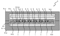
- the apparatus 5 shown in FIGS. 4 to 5 is used.
- the device 5 includes a first terminal 11 of the first electronic component 1 having a first terminal 11 having a solder layer 112 on the surface, and a second terminal 21 joined to the first terminal 11 of the first electronic component 1.
- the resin layer 3 including the flux active compound and the thermosetting resin is disposed between the second terminal 21 of the second electronic component 2 and the laminate 4 is formed, the first terminal 11, This is a device for contacting the two terminals 21.
- the apparatus 5 includes a jig 53 that is a clamping member that simultaneously clamps the plurality of stacked bodies 4. More specifically, the apparatus 5 includes a furnace (heating furnace) 51 in which a plurality of laminated bodies 4 are disposed, an upper heating plate 521 and a lower heating plate 522 that are press members disposed in the furnace 51. And a jig 53.
- the furnace 51 includes an upper mold 511 and a lower mold 512, and an upper heating plate 521 and a lower heating plate 522 are arranged in a space formed by the upper mold 511 and the lower mold 512.
- the upper heating plate 521 and the lower heating plate 522 are arranged to face each other, and the jig 53 and the plurality of laminated bodies 4 are arranged between the upper heating plate 521 and the lower heating plate 522.
- the pair of hot plates 521 and 522 are at a temperature lower than the melting point of the solder layer 112.
- the jig 53 includes an upper pressure member 531 having a groove and a flat plate-like lower pressure member 532.
- a plurality of stacked bodies 4 are arranged between the upper pressure member 531 and the lower pressure member 532.
- the upper pressure member 531 has a plate shape and a planar rectangular shape.
- the upper pressure member 531 is formed with a plurality of grooves 531A, and some of the grooves 531A intersect each other.
- the grooves 531A are formed in a lattice shape.
- the region 531B partitioned by the groove 531A comes into contact with the second electronic component 2 of the laminate 4.
- the second electronic component 2 of one stacked body 4 comes into contact with one region 531B.
- the lower pressure member 532 has a planar rectangular shape, and no groove is formed in the lower pressure member 532, and the lower pressure member 532 is made of a plate material having a flat surface.
- the lower pressure member 532 and the surface of the upper pressure member 531 on which the groove 531A is formed are opposed to each other.
- the first electronic component 1 of the stacked body 4 is in contact with the lower pressure member 532.
- the material of the lower pressure member 532 and the upper pressure member 531 is not particularly limited, and examples thereof include a metal plate and a ceramic plate.
- Examples of the metal plate include a stainless plate, a titanium plate, and a lead plate.
- Examples of the ceramic plate include a glass plate, an alumina plate, a silicon nitride plate, and a zirconia plate. However, those having good thermal conductivity are preferred.
- a plurality of laminated bodies 4 are arranged between the upper pressure member 531 and the lower pressure member 532 of the jig 53, and the upper pressure member 531 and the lower pressure member 532.
- a plurality of laminates 4 are sandwiched between members 532.
- the width W1 of the groove 531A (the length in the direction orthogonal to the extending direction of the groove 531A) is larger than the gap W2 between the adjacent stacked bodies 4.
- the end surface (side surface) of the second electronic component 2 that abuts on the region 531B defined by the groove 531A protrudes inside the groove 531A from the side surface 531C of the groove 531A.
- the region 531 ⁇ / b> B defined by the groove 531 ⁇ / b> A having the width W ⁇ b> 1 of the upper pressure member 531 is formed in a shape located outside the second terminal 21 of the second electronic component 2.
- the resin layers 3 of the adjacent laminates 4 are formed continuously, but since a gap is formed between the adjacent second electronic components 2, the resin layer 3 is connected from the gap. A part of the resin sheet constituted by is exposed. The exposed portion of the resin sheet faces the groove 531A.
- FIG. 6 is a view showing a state in which a plurality of stacked bodies 4 are sandwiched between the upper pressure member 531 and the lower pressure member 532.
- the jig 53 and the plurality of stacked bodies 4 are transported into the furnace 51.
- a transport film or the like may be used.
- the upper heating plate 521 and the lower heating plate 522 are in a heated state in advance. Thereafter, the upper mold 511 is moved to the lower mold 512 side, and the gap between the upper mold 511 and the lower mold 512 is closed. The lower heat plate 522 comes into contact with the lower pressure member 532 of the jig 53 (see FIG. 4).
- the upper heating plate 521 is moved downward, and the upper heating plate 521 comes into contact with the upper pressure member 531 of the jig 53.
- the upper pressing member 531 of the jig 53 is pushed downward by the upper heating plate 521, the jig 53 is clamped by the lower heating plate 522 and the upper heating plate 521, and the upper pressing members 531, 532 of the jig 53 A plurality of laminated bodies 4 will be pinched.
- the plurality of laminates 4 are less than the melting point of the solder layer 112 and less than the curing temperature of the resin layer 3, that is, less than the curing temperature of the thermosetting resin of the resin layer 3 (the thermosetting resin contained in the resin layer 3
- the second terminal 21 is made of resin so that the first terminal 11 and the second terminal 21 come into contact with each other while being heated at a temperature lower than the C-stage in accordance with JISK6900). It will sink into layer 3.
- the upper mold 511 and the lower mold 512 are separated from each other, and the plurality of stacked bodies 4 are carried out from the furnace 51.
- the plurality of stacked bodies 4 may be clamped under a vacuum. Thereby, generation
- the plurality of stacked bodies 4 are heated to the melting point or higher of the solder layer 112 of the first terminal 11, and the first terminal 11 and the second terminal 21 are soldered. .
- the apparatus 6 can heat the laminated body 4 in a pressurized atmosphere.
- the structure of the apparatus 6 includes, for example, a container 61 that houses the laminated body 4 and a fluid for introducing the fluid into the container 61. And a pipe 62.
- the container 61 is characterized by being a pressure vessel. After the laminated body 4 is installed in the container 61, the laminated body 4 is heated by heating from the pipe 62 and flowing a pressurized fluid into the container 61. Pressurize.
- the laminated body 4 can also be heated by flowing the fluid from the pipe 62 into the container 61 and heating the container 61 in a pressurized atmosphere.
- the material of the container 61 include metals, such as stainless steel, titanium, copper, and alloys thereof.
- the pressure applied when the laminate 4 is pressurized with a fluid is 0.1 to 10 MPa, preferably 0.5 to 5 MPa. By doing in this way, it becomes difficult to generate voids in the cured resin layer 3.
- pressurizing with a fluid refers to making the pressure of the atmosphere of the laminated body 4 higher than atmospheric pressure by the applied pressure. That is, the applied pressure of 10 MPa indicates that the pressure acting on the laminate is 10 MPa greater than the atmospheric pressure.
- the laminated body 4 After installing the laminated body 4 in the container 61, the laminated body 4 is heated and the laminated body 4 is pressurized.
- the fluid that pressurizes the stacked body 4 is introduced into the container 61 from the pipe 62 and pressurizes the stacked body 4.
- a non-oxidizing gas such as nitrogen gas or argon gas, or a gas such as air is preferable.
- a non-oxidizing gas By using a non-oxidizing gas, the first terminal 11 and the second terminal 21 can be joined better.
- the non-oxidizing gas means inert gas or nitrogen gas.
- the laminated body 4 After the temperature of the laminated body 4 reaches the melting point of the solder layer 112, the laminated body 4 is heated and pressurized for a predetermined time while maintaining the temperature and pressure in the container 61. Thereby, the resin layer 3 in the laminated body 4 will harden
- the laminate 4 is taken out from the apparatus 6 and the laminate 4 is cured again as necessary.
- an electronic device can be obtained (see FIG. 9).
- the first terminal 11 and the second terminal 21 are joined by the solder layer 112, and the tip of the second terminal 21 is in a state of being bitten into the solder layer 112.
- a plurality of separated electronic devices can be obtained by cutting between the first electronic components 1 and between the resin layers 3 according to the dotted cutting line shown in FIG.
- the plurality of stacked bodies 4 are simultaneously pressed from the stacking direction of the stacked bodies 4 while heating the plurality of stacked bodies 4. Thereby, while the 1st electronic component 1 and the 2nd electronic component 2 of the 1st laminated body 4 are clamped, it is suppressed that hardening of the resin layer 3 of the other laminated body 4 advances. Is done. Therefore, a highly reliable electronic device can be manufactured stably.
- the laminated body 4 is pressurized with the pressurized fluid and the resin layer 3 is cured, the generation of voids such as bubbles in the cured product of the resin layer 3 can be suppressed. Furthermore, when soldering the first terminal 11 and the second terminal 21, if the laminate 4 is pressurized with a fluid, the density of the resin layer 3 is increased and the volume is reduced. A force can be applied in the direction in which the second terminal 21 is crimped.
- the laminate 4 is pressurized with a fluid, the resin flow due to foaming of the resin layer 3 can be suppressed, and the first terminal 11 and the second terminal 21 The deviation can be reliably reduced.
- the groove 531A is formed in the upper pressure member 531 that sandwiches the stacked body 4.
- the resin layer 3 of the laminate 4 may protrude from the laminate 4, but the protruded resin layer 3 can escape into the groove 531 ⁇ / b> A. Thereby, it is possible to prevent the resin from entering between the second electronic component 2 and the upper pressure member 531.
- the end surface of the second electronic component 2 that abuts on the region 531B defined by the groove 531A protrudes inside the groove 531A from the side surface 531C of the groove 531A.
- the resin protruding from the laminated body 4 may crawl up along the end surface of the second electronic component 2 of the laminated body 4. Since the side surface 531C of the groove 531A does not protrude to the inside of the groove 531A from the end surface of the second electronic component 2, the resin scooping up the end surface of the second electronic component 2 adheres to the upper pressure member 531. This can be suppressed. Therefore, contamination of the upper pressure member 531 with the resin can be prevented.
- the groove 531A is not formed in the upper pressure member 531, there is a possibility that the resin protruding from the laminate 4 adheres to the member and the surface of the member on the laminate 4 side is not flat. is there. Therefore, the load acting on the laminate 4 may vary.
- the adhesion of the resin to the upper pressure member 531 can be prevented as described above, it is possible to suppress the occurrence of variations in the load acting on the laminate 4.
- the present invention is not limited to the above-described embodiment, and modifications, improvements, and the like within the scope that can achieve the object of the present invention are included in the present invention.
- the jig 53 is used in the device 5, but the present invention is not limited to this, and the jig 53 may not be used.
- the first electronic components 1 and the resin layers 3 were connected, it is not restricted to this.
- the first electronic components 1 and the resin layers 3 may be separated in advance, and there may be a gap (gap) between the first electronic components 1 and between the resin layers 3.
- the upper pressure member 531 is brought into contact with the second electronic component 2, but the present invention is not limited to this, and the upper pressure member 531 may be brought into contact with the first electronic component 1. Good.
- the upper pressure member 531 is in contact with the first electronic component 1, and in the other laminate 4, the upper pressure member 531 is in contact with the second electronic component 2. It may be. However, from the viewpoint of the stability of bonding between the terminals, it is preferable that the parts contacting the upper pressure member 531 are the same parts as in the above embodiment.
- the groove 531A that divides the region 531B in contact with the second electronic component 2 of the laminate 4 is formed only on the lower surface, and the upper pressure member 531 having a flat upper surface is illustrated.
- the groove 533A identical to the groove 531A on the lower surface is also formed on the upper surface, and the region 533B is partitioned, so that the upper and lower symmetrical upper pressure members are formed.
- the member 533 and the like can also be implemented.
- the up-down direction here corresponds to the up-down direction in FIG. That is, it coincides with the stacking direction of the stacked body 4.
- the upper pressing member 533 is symmetrical in the vertical direction, it is possible to prevent the bending due to the pressing well, and to press the plurality of second electronic components 2 to the first electronic component 1 more evenly.
- the upper pressure member 533 as described above is vertically symmetric, it can be prevented from being bent in the vertical direction due to pressure during manufacturing.
- a laminated body is heated by the hot plates 521 and 522 which are press members, heating the laminated body 4 at the temperature below the curing temperature of the resin layer 3. Only the pressurization of the laminate 4 along the four lamination directions is illustrated.
- the laminate 4 when the laminate 4 is mechanically pressurized in this manner, the laminate 4 may be further pressurized by a fluid such as air (not shown). In this case, not only can the laminated body 4 be pressed uniformly, but also the expansion of bubbles generated in the resin layer 3 can be prevented.
- a fluid such as air
- the laminate 4 may be heated at a temperature that is lower than the curing temperature of the resin layer 3 and the viscosity of the resin layer 3 is 1 Pa ⁇ s or more and 10,000 Pa ⁇ s or less. Moreover, in the process of obtaining the above-mentioned laminated body 4, the laminated body 4 may be arrange
- the pressure of the fluid that pressurizes the stacked body 4 is an internal pressure that opens the upper mold 511 and the lower mold 512 of the furnace 51. Therefore, as shown in FIG. 11, the pressure for closing the upper mold 511 and the lower mold 512 of the furnace 51, the pressure of the hot plates 521 and 522 that directly pressurize the stacked body 4, and the furnace that pressurizes the stacked body 4. It is preferable that the air pressure in 51 can be controlled separately.
Landscapes
- Chemical & Material Sciences (AREA)
- Engineering & Computer Science (AREA)
- Mechanical Engineering (AREA)
- Health & Medical Sciences (AREA)
- Chemical Kinetics & Catalysis (AREA)
- Medicinal Chemistry (AREA)
- Polymers & Plastics (AREA)
- Organic Chemistry (AREA)
- Electric Connection Of Electric Components To Printed Circuits (AREA)
- Wire Bonding (AREA)
Abstract
Description
HOOC-(CH2)n-COOH (1)
式(1)中、nは、20以下の自然数を表す。
(1)フラックス活性化合物を含有する樹脂組成物をフィルム状に成形した樹脂フィルムを用意し、この樹脂フィルムを、第一電子部品1、または、第二電子部品2にラミネートする方法、
(2)フラックス活性化合物を含有する液状の樹脂組成物を用意し、この液状の樹脂組成物を、第一電子部品1、または、第二電子部品2の表面に塗布する方法、
(3)フラックス活性化合物を含有する樹脂組成物が溶剤に溶解、または、分散されている樹脂ワニスを用意し、この樹脂ワニスを、第一電子部品1、または、第二電子部品2の表面に塗布し、次いで、樹脂ワニス中の溶剤を揮発させる方法、
が挙げられる。なお、方法(2)に係る液状の樹脂組成物は、溶剤を含有しない。
Claims (20)
- 表面に半田層を有する第一端子を有する第一電子部品と、この第一電子部品の前記第一端子に接合される第二端子を有する第二電子部品とを備える電子装置の製造方法であって、
前記第一電子部品の第一端子と、前記第二電子部品の第二端子との間にフラックス活性化合物と、熱硬化性樹脂とを含む樹脂層を配置して積層体を得る工程と、
前記積層体を前記第一端子の前記半田層の融点以上に加熱して、前記第一端子と、前記第二端子とを半田接合させる工程と、
流体により前記積層体を加圧しながら、前記樹脂層を硬化させる工程とを含み、
前記積層体を得る前記工程では、
複数の第一電子部品の第一端子と、複数の第二電子部品の第二端子とをそれぞれ対向配置させ、各第一端子と各第二端子との間に前記樹脂層を配置して複数の積層体を形成し、複数の積層体を加熱しながら、前記複数の積層体を同時に前記積層体の積層方向から挟圧する電子装置の製造方法。 - 請求項1に記載の電子装置の製造方法において、
前記複数の積層体は面内方向に配列されている電子装置の製造方法。 - 請求項1または2に記載の電子装置の製造方法において、
積層体を得る前記工程では、
前記複数の積層体を一対の挟圧部材で挟圧し、
前記一対の挟圧部材のうち、一方の挟圧部材は、溝が形成された部材であり、
溝が形成された前記部材を前記積層体に当接させた際に、
一方の挟圧部材の前記溝で区画された各領域がそれぞれ前記積層体の第一電子部品または第二電子部品に当接し、かつ、前記溝で区画された前記領域に当接する第一電子部品または第二電子部品の端面が、前記溝の側面よりも溝内側に突出する電子装置の製造方法。 - 請求項3に記載の電子装置の製造方法において、
溝が形成された前記部材を前記積層体に当接させた際に、
前記溝で区画された前記領域には、各積層体の第一電子部品および第二電子部品のうち一方の部品が当接し、
複数の積層体の各樹脂層は連なって、樹脂シートを構成し、
前記積層体の積層方向からみて、隣接する積層体の前記一方の部品間から前記樹脂シートの一部が露出し、
溝が形成された前記部材を前記積層体に当接させた際に、露出した前記樹脂シートの一部が前記溝と対向する電子装置の製造方法。 - 請求項1ないし4の何れか一項に記載の電子装置の製造方法において、
積層体を得る前記工程では、
前記樹脂層の硬化温度未満の温度で前記積層体を加熱しながら、プレス部材により前記積層体の積層方向に沿って前記積層体を加圧するとともに、流体により前記積層体を加圧する電子装置の製造方法。 - 請求項5に記載の電子装置の製造方法において、
前記積層体を得る前記工程において、
前記プレス部材は、熱板であり、前記熱板を積層体に当接させることで、前記積層体が加熱される電子装置の製造方法。 - 請求項5または6に記載の電子装置の製造方法において、
前記積層体を得る前記工程において、容器内に前記積層体を配置し、前記容器内に前記流体を導入して、前記流体により前記積層体を加圧する電子装置の製造方法。 - 請求項1または2に記載の電子装置の製造方法において、
積層体を得る前記工程は、
前記複数の積層体を一対の挟圧部材で挟圧する工程と、
前記樹脂層の硬化温度未満の温度で前記積層体を加熱しながら、前記一対の狭圧部材をプレス部材によって前記積層体の積層方向から狭圧することにより、前記積層体の積層方向に沿って前記積層体を加圧するとともに、流体により前記積層体を加圧する工程と、
を含み、
前記一対の挟圧部材のうち、一方の挟圧部材は、溝が形成された部材であり、
溝が形成された前記部材を前記積層体に当接させた際に、
一方の挟圧部材の前記溝で区画された各領域がそれぞれ前記積層体の第一電子部品または第二電子部品に当接し、かつ、前記溝で区画された前記領域に当接する第一電子部品または第二電子部品の端面が、前記溝の側面よりも溝内側に突出する電子装置の製造方法。 - 請求項1ないし8の何れか一項に記載の電子装置の製造方法において、
前記積層体を得る前記工程では、
前記樹脂層の粘度が1Pa・s以上、10000Pa・s以下となる温度で前記積層体を加熱する電子装置の製造方法。 - 表面に半田層を有する第一端子を有する第一電子部品の前記第一端子と、この第一電子部品の前記第一端子に接合される第二端子を有する第二電子部品の前記第二端子との間に、フラックス活性化合物と、熱硬化性樹脂とを含む樹脂層を配置して、積層体を形成した後、前記第一端子と、前記第二端子とを接触させるための装置であって、
複数の積層体を同時に挟圧する挟圧部材を備える装置。 - 請求項10に記載の装置であって、
前記狭圧部材は、面内方向に配列された前記複数の積層体を同時に狭圧する装置。 - 請求項10または11に記載の装置であって、
前記挟圧部材は、前記複数の積層体を挟圧する一対の挟圧部材を有し、
前記一対の挟圧部材のうち、少なくとも一方の挟圧部材は、溝が形成された部材であり、
溝が形成された前記部材を前記積層体に当接させた際に、
一方の挟圧部材の前記溝で区画された各領域をそれぞれ前記積層体の第一電子部品または第二電子部品に当接し、かつ、前記溝で区画された前記領域に当接する第一電子部品または第二電子部品の端面が、前記溝の側面よりも溝内側に突出するように構成されている装置。 - 請求項10ないし12の何れか一項に記載の装置において、
前記樹脂層の硬化温度未満の温度で前記積層体を加熱しながら、プレス部材により前記積層体の積層方向に沿って前記積層体を加圧するとともに、流体により前記積層体を加圧するように構成されている装置。 - 請求項13に記載の装置において、
前記プレス部材は、熱板であり、前記熱板を積層体に当接させることで、前記積層体を加熱するように構成されている装置。 - 請求項13または14に記載の装置において、
容器内に前記積層体を配置し、前記容器内に前記流体を導入して、前記流体により前記積層体を加圧するように構成されている装置。 - 請求項10ないし15の何れか一項に記載の装置において、
前記積層体の前記樹脂層の粘度が1Pa・s以上、10000Pa・s以下となる温度で前記積層体を加熱するように構成されている装置。 - 請求項12に記載の装置であって、
一対の前記挟圧部材のうち前記溝が形成されている少なくとも一方の前記狭圧部材は、上下対称に形成されている装置。 - 請求項17に記載の装置であって、
前記一対の狭圧部材のうち少なくとも一方の狭圧部材は、前記第二電子部品に当接する下面に形成されている前記溝と上下対称に上面にも溝が形成されている装置。 - 請求項17または18に記載された装置の一対の挟圧部材であって、
前記溝が形成されている少なくとも一方の狭圧部材は、上下対称に形成されている一対の挟圧部材。 - 請求項19に記載の一対の挟圧部材であって、
少なくとも一方の狭圧部材は、前記第二電子部品に当接する下面に形成されている前記溝と上下対称に上面にも溝が形成されている一対の挟圧部材。
Priority Applications (3)
| Application Number | Priority Date | Filing Date | Title |
|---|---|---|---|
| CN2011800204408A CN102859674A (zh) | 2010-04-23 | 2011-04-13 | 电子装置的制造方法和装置及其一对夹压构件 |
| KR1020127030656A KR20130054283A (ko) | 2010-04-23 | 2011-04-13 | 전자 장치의 제조 방법 및 장치, 그 1 쌍의 협압 부재 |
| JP2012511532A JPWO2011132384A1 (ja) | 2010-04-23 | 2011-04-13 | 電子装置の製造方法および装置、その一対の挟圧部材 |
Applications Claiming Priority (6)
| Application Number | Priority Date | Filing Date | Title |
|---|---|---|---|
| JP2010099553 | 2010-04-23 | ||
| JP2010-099553 | 2010-04-23 | ||
| JP2010150827 | 2010-07-01 | ||
| JP2010-150827 | 2010-07-01 | ||
| JP2010186870 | 2010-08-24 | ||
| JP2010-186870 | 2010-08-24 |
Publications (1)
| Publication Number | Publication Date |
|---|---|
| WO2011132384A1 true WO2011132384A1 (ja) | 2011-10-27 |
Family
ID=44833928
Family Applications (1)
| Application Number | Title | Priority Date | Filing Date |
|---|---|---|---|
| PCT/JP2011/002184 Ceased WO2011132384A1 (ja) | 2010-04-23 | 2011-04-13 | 電子装置の製造方法および装置、その一対の挟圧部材 |
Country Status (5)
| Country | Link |
|---|---|
| JP (1) | JPWO2011132384A1 (ja) |
| KR (1) | KR20130054283A (ja) |
| CN (1) | CN102859674A (ja) |
| TW (1) | TW201222689A (ja) |
| WO (1) | WO2011132384A1 (ja) |
Cited By (2)
| Publication number | Priority date | Publication date | Assignee | Title |
|---|---|---|---|---|
| JP2013222859A (ja) * | 2012-04-17 | 2013-10-28 | Sumitomo Bakelite Co Ltd | 積層体の製造方法 |
| JP2014127477A (ja) * | 2012-12-25 | 2014-07-07 | Sumitomo Bakelite Co Ltd | 半導体装置の製造方法 |
Families Citing this family (2)
| Publication number | Priority date | Publication date | Assignee | Title |
|---|---|---|---|---|
| CN111876580B (zh) * | 2016-02-09 | 2022-04-29 | 阿尔卑斯阿尔派株式会社 | 非晶态合金薄带的层叠体的热处理装置 |
| KR102539717B1 (ko) * | 2021-06-29 | 2023-06-05 | (주)나노테크 | 압력분포 조절이 가능한 브레이징 용접용 지그 |
Citations (2)
| Publication number | Priority date | Publication date | Assignee | Title |
|---|---|---|---|---|
| JP2004311709A (ja) * | 2003-04-07 | 2004-11-04 | Renesas Technology Corp | 半導体装置の製造方法および半導体製造装置 |
| WO2006082744A1 (ja) * | 2005-02-02 | 2006-08-10 | Sony Chemical & Information Device Corporation | 電気部品の実装装置 |
Family Cites Families (8)
| Publication number | Priority date | Publication date | Assignee | Title |
|---|---|---|---|---|
| JP2903697B2 (ja) * | 1990-11-06 | 1999-06-07 | セイコーエプソン株式会社 | 半導体装置の製造方法及び半導体装置の製造装置 |
| JPH06349892A (ja) * | 1993-06-10 | 1994-12-22 | Matsushita Electric Ind Co Ltd | 半導体装置の製造方法 |
| JP3301075B2 (ja) * | 1999-04-20 | 2002-07-15 | ソニーケミカル株式会社 | 半導体装置の製造方法 |
| JP3537400B2 (ja) * | 2000-03-17 | 2004-06-14 | 松下電器産業株式会社 | 半導体内蔵モジュール及びその製造方法 |
| JP2002110744A (ja) * | 2000-09-26 | 2002-04-12 | Matsushita Electric Ind Co Ltd | 半導体実装装置、および半導体実装方法 |
| JP3921459B2 (ja) * | 2003-07-11 | 2007-05-30 | ソニーケミカル&インフォメーションデバイス株式会社 | 電気部品の実装方法及び実装装置 |
| JP4692101B2 (ja) * | 2005-06-27 | 2011-06-01 | ソニー株式会社 | 部品接合方法 |
| JP2008147601A (ja) * | 2006-12-13 | 2008-06-26 | Yoshihiro Shimada | フリップチップ接合方法及び半導体装置の製造方法 |
-
2011
- 2011-04-13 WO PCT/JP2011/002184 patent/WO2011132384A1/ja not_active Ceased
- 2011-04-13 JP JP2012511532A patent/JPWO2011132384A1/ja active Pending
- 2011-04-13 KR KR1020127030656A patent/KR20130054283A/ko not_active Withdrawn
- 2011-04-13 CN CN2011800204408A patent/CN102859674A/zh active Pending
- 2011-04-21 TW TW100113854A patent/TW201222689A/zh unknown
Patent Citations (2)
| Publication number | Priority date | Publication date | Assignee | Title |
|---|---|---|---|---|
| JP2004311709A (ja) * | 2003-04-07 | 2004-11-04 | Renesas Technology Corp | 半導体装置の製造方法および半導体製造装置 |
| WO2006082744A1 (ja) * | 2005-02-02 | 2006-08-10 | Sony Chemical & Information Device Corporation | 電気部品の実装装置 |
Cited By (2)
| Publication number | Priority date | Publication date | Assignee | Title |
|---|---|---|---|---|
| JP2013222859A (ja) * | 2012-04-17 | 2013-10-28 | Sumitomo Bakelite Co Ltd | 積層体の製造方法 |
| JP2014127477A (ja) * | 2012-12-25 | 2014-07-07 | Sumitomo Bakelite Co Ltd | 半導体装置の製造方法 |
Also Published As
| Publication number | Publication date |
|---|---|
| TW201222689A (en) | 2012-06-01 |
| CN102859674A (zh) | 2013-01-02 |
| JPWO2011132384A1 (ja) | 2013-07-18 |
| KR20130054283A (ko) | 2013-05-24 |
Similar Documents
| Publication | Publication Date | Title |
|---|---|---|
| JP5780228B2 (ja) | 半導体装置の製造方法 | |
| JP5533663B2 (ja) | 電子装置の製造方法 | |
| WO2013027832A1 (ja) | 半導体装置の製造方法、ブロック積層体及び逐次積層体 | |
| CN102668051A (zh) | 电子装置的制造方法、电子装置以及制造电子装置的设备 | |
| JP2012104782A (ja) | 半導体装置の製造方法および装置 | |
| CN101960932A (zh) | 焊料连接的方法、电子器件及其制造方法 | |
| JP5853754B2 (ja) | 半導体装置の製造方法 | |
| JP2013033952A (ja) | 半導体装置の製造方法 | |
| JP6032345B2 (ja) | 接着フィルム | |
| JP5948723B2 (ja) | 電子装置の製造方法 | |
| WO2012026091A1 (ja) | 電子装置の製造方法 | |
| JPWO2011132384A1 (ja) | 電子装置の製造方法および装置、その一対の挟圧部材 | |
| JP6226106B2 (ja) | 電子装置の製造方法 | |
| JP2014056954A (ja) | 半導体装置の製造方法および半導体装置 | |
| JP2012160668A (ja) | 電子部品の製造方法 | |
| JP2011228620A (ja) | 電子装置の製造方法および電子装置の製造装置 | |
| JP2013045945A (ja) | 半導体装置の製造方法 | |
| JP2017028067A (ja) | 回路部材の接続方法 | |
| JP2016036041A (ja) | 半導体装置の製造方法 | |
| JP5853944B2 (ja) | 半導体装置の製造方法 | |
| JP2017038081A (ja) | 半導体装置 | |
| JP2011159859A (ja) | 電子部品の製造方法及び電子部品 | |
| JP2011187489A (ja) | 電子部品の製造方法、電子部品、および電子装置の製造方法および電子装置 |
Legal Events
| Date | Code | Title | Description |
|---|---|---|---|
| WWE | Wipo information: entry into national phase |
Ref document number: 201180020440.8 Country of ref document: CN |
|
| 121 | Ep: the epo has been informed by wipo that ep was designated in this application |
Ref document number: 11771727 Country of ref document: EP Kind code of ref document: A1 |
|
| WWE | Wipo information: entry into national phase |
Ref document number: 2012511532 Country of ref document: JP |
|
| NENP | Non-entry into the national phase |
Ref country code: DE |
|
| ENP | Entry into the national phase |
Ref document number: 20127030656 Country of ref document: KR Kind code of ref document: A |
|
| 122 | Ep: pct application non-entry in european phase |
Ref document number: 11771727 Country of ref document: EP Kind code of ref document: A1 |