WO2011132288A1 - 光電変換素子用電極の製造方法 - Google Patents
光電変換素子用電極の製造方法 Download PDFInfo
- Publication number
- WO2011132288A1 WO2011132288A1 PCT/JP2010/057145 JP2010057145W WO2011132288A1 WO 2011132288 A1 WO2011132288 A1 WO 2011132288A1 JP 2010057145 W JP2010057145 W JP 2010057145W WO 2011132288 A1 WO2011132288 A1 WO 2011132288A1
- Authority
- WO
- WIPO (PCT)
- Prior art keywords
- film
- electrode
- photocatalyst film
- photoelectric conversion
- conversion element
- Prior art date
- Legal status (The legal status is an assumption and is not a legal conclusion. Google has not performed a legal analysis and makes no representation as to the accuracy of the status listed.)
- Ceased
Links
Images

Classifications
-
- H—ELECTRICITY
- H01—ELECTRIC ELEMENTS
- H01G—CAPACITORS; CAPACITORS, RECTIFIERS, DETECTORS, SWITCHING DEVICES, LIGHT-SENSITIVE OR TEMPERATURE-SENSITIVE DEVICES OF THE ELECTROLYTIC TYPE
- H01G9/00—Electrolytic capacitors, rectifiers, detectors, switching devices, light-sensitive or temperature-sensitive devices; Processes of their manufacture
- H01G9/20—Light-sensitive devices
- H01G9/2027—Light-sensitive devices comprising an oxide semiconductor electrode
- H01G9/2031—Light-sensitive devices comprising an oxide semiconductor electrode comprising titanium oxide, e.g. TiO2
-
- H—ELECTRICITY
- H01—ELECTRIC ELEMENTS
- H01M—PROCESSES OR MEANS, e.g. BATTERIES, FOR THE DIRECT CONVERSION OF CHEMICAL ENERGY INTO ELECTRICAL ENERGY
- H01M14/00—Electrochemical current or voltage generators not provided for in groups H01M6/00 - H01M12/00; Manufacture thereof
-
- H—ELECTRICITY
- H10—SEMICONDUCTOR DEVICES; ELECTRIC SOLID-STATE DEVICES NOT OTHERWISE PROVIDED FOR
- H10F—INORGANIC SEMICONDUCTOR DEVICES SENSITIVE TO INFRARED RADIATION, LIGHT, ELECTROMAGNETIC RADIATION OF SHORTER WAVELENGTH OR CORPUSCULAR RADIATION
- H10F10/00—Individual photovoltaic cells, e.g. solar cells
-
- H—ELECTRICITY
- H01—ELECTRIC ELEMENTS
- H01G—CAPACITORS; CAPACITORS, RECTIFIERS, DETECTORS, SWITCHING DEVICES, LIGHT-SENSITIVE OR TEMPERATURE-SENSITIVE DEVICES OF THE ELECTROLYTIC TYPE
- H01G9/00—Electrolytic capacitors, rectifiers, detectors, switching devices, light-sensitive or temperature-sensitive devices; Processes of their manufacture
- H01G9/20—Light-sensitive devices
- H01G9/2059—Light-sensitive devices comprising an organic dye as the active light absorbing material, e.g. adsorbed on an electrode or dissolved in solution
-
- Y—GENERAL TAGGING OF NEW TECHNOLOGICAL DEVELOPMENTS; GENERAL TAGGING OF CROSS-SECTIONAL TECHNOLOGIES SPANNING OVER SEVERAL SECTIONS OF THE IPC; TECHNICAL SUBJECTS COVERED BY FORMER USPC CROSS-REFERENCE ART COLLECTIONS [XRACs] AND DIGESTS
- Y02—TECHNOLOGIES OR APPLICATIONS FOR MITIGATION OR ADAPTATION AGAINST CLIMATE CHANGE
- Y02E—REDUCTION OF GREENHOUSE GAS [GHG] EMISSIONS, RELATED TO ENERGY GENERATION, TRANSMISSION OR DISTRIBUTION
- Y02E10/00—Energy generation through renewable energy sources
- Y02E10/50—Photovoltaic [PV] energy
- Y02E10/542—Dye sensitized solar cells
-
- Y—GENERAL TAGGING OF NEW TECHNOLOGICAL DEVELOPMENTS; GENERAL TAGGING OF CROSS-SECTIONAL TECHNOLOGIES SPANNING OVER SEVERAL SECTIONS OF THE IPC; TECHNICAL SUBJECTS COVERED BY FORMER USPC CROSS-REFERENCE ART COLLECTIONS [XRACs] AND DIGESTS
- Y02—TECHNOLOGIES OR APPLICATIONS FOR MITIGATION OR ADAPTATION AGAINST CLIMATE CHANGE
- Y02P—CLIMATE CHANGE MITIGATION TECHNOLOGIES IN THE PRODUCTION OR PROCESSING OF GOODS
- Y02P70/00—Climate change mitigation technologies in the production process for final industrial or consumer products
- Y02P70/50—Manufacturing or production processes characterised by the final manufactured product
Definitions
- a transparent conductive film and an electrode having a photocatalytic film thereon are disposed on a transparent substrate, and a counter electrode having at least a conductive member is disposed on the counter substrate at a predetermined interval, and an electrolyte is disposed between the electrodes. More specifically, the present invention relates to a method for manufacturing the electrode.
- a photoelectric conversion element such as a dye-sensitized solar cell is formed by forming a transparent conductive film on a transparent substrate such as a glass plate and forming a photocatalytic film made of a metal oxide such as titanium oxide on the transparent conductive film.
- An electrode formed by adsorbing a photosensitizing dye such as a ruthenium complex on the film and a counter electrode formed by forming a transparent conductive film on a counter electrode transparent substrate are arranged opposite to each other.
- the thing which intervened the electrolyte layer which becomes is known (patent document 1).
- the photocatalyst film made of a metal oxide such as titanium oxide has a problem that if it contains moisture, the adsorption of the photosensitizing dye is inhibited and the photoelectric conversion efficiency is lowered. Therefore, before adsorption of the photosensitizing dye, the photocatalyst film is placed in a chamber containing a dehydrating agent and a desiccant and the atmosphere in the chamber is circulated, or the photocatalyst film is placed in the chamber and the inside of the chamber is depressurized. It has been proposed to increase the adsorptivity of the photosensitizing dye by dehydrating the photocatalyst film by such a method (Patent Document 2).
- an object of the present invention is to provide a method for producing an electrode for a photoelectric conversion element that can dehydrate the photocatalyst film at a low cost in a short time without requiring a large-scale apparatus.
- the invention according to claim 1 is an electrode manufacturing method in which a transparent conductive film is formed on a transparent substrate, a photocatalyst film is formed thereon, and a photosensitizing dye is adsorbed on the photocatalyst film. Before the photosensitizing dye is adsorbed, the photocatalyst film is immersed in an alcohol having an azeotropic temperature of 150 ° C. or less with water and then heated to dehydrate the photocatalyst film by azeotropy of water and alcohol. It is the manufacturing method of the electrode for photoelectric conversion elements characterized by the above-mentioned.
- the invention according to claim 2 is the method for producing an electrode for a photoelectric conversion element according to claim 1, wherein the alcohol is 1-propanol or 1-butanol.
- the transparent substrate is in the form of a film or sheet, and the photocatalyst film is formed, the photocatalyst film is dehydrated, and the photosensitizing dye is adsorbed onto the photocatalyst film continuously. It is a manufacturing method of the electrode for photoelectric conversion elements of description.
- the transparent substrate having the photocatalytic film is immersed in an alcohol having an azeotropic temperature of 150 ° C. or lower and then heated before the photosensitizing dye is adsorbed on the photocatalytic film.
- the photocatalyst film can be dehydrated in a short time at a low cost without requiring a large apparatus such as a chamber as in the prior art.
- the method for producing the electrode including the dehydration step can be continuously performed by continuously supplying a film or sheet-like transparent substrate.
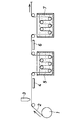
- FIG. 3 is a flow sheet schematically showing a method for producing the photoelectric conversion element electrode of Example 1.
- FIG. 5 is a vertical longitudinal sectional view showing a photoelectric conversion element of Reference Example 1.
- a transparent conductive film is formed on a transparent substrate, and a photocatalytic film is formed thereon.
- the transparent substrate a synthetic resin plate, a glass plate or the like is appropriately used, but a thermoplastic resin film such as a PEN (polyethylene naphthalate) film is preferable.
- the synthetic resin may be polyethylene terephthalate, polyester, polycarbonate, polyolefin, or the like.
- the thickness of the transparent substrate is preferably several tens of ⁇ m to 1 mm.
- the transparent conductive film there are various methods for forming the transparent conductive film, such as ionization vapor deposition and CVD, but it is particularly preferable to use sputtering.
- a metal target in the sputtering method materials of tin-doped indium oxide (ITO), fluorine-doped tin oxide (FTO), tin oxide (SnO2), indium zinc oxide (IZO), and zinc oxide (ZnO) for transparent conductive films In—Sn alloy, Zn, In—Zn alloy, Sn, Ga—Zn alloy, Al—Zn alloy, and the like are preferably used.
- the thickness of the transparent conductive film is preferably several tens to several hundreds nm.
- the metal oxide layer (photocatalytic film) formed on the transparent conductive film is preferably titanium oxide or zinc oxide.
- the method of forming the photocatalyst film is not particularly limited, but a method of applying a paste-like mixed solution of metal oxide particles having a particle diameter of 20 to 60 ⁇ m dispersed in a solvent such as alcohol onto a transparent conductive film with a squeegee, A method of electrostatically applying a metal oxide sol can be applied.
- the electrostatic coating device is on the negative side and the transparent conductive film of the transparent electrode that is the object to be coated is on the positive side.
- the metal oxide sprayed from the spray nozzle of the coating device is charged to the negative side and applied to the surface of the transparent conductive film.
- metal compound used as a starting material for the metal oxide sol examples include metal alkoxides, metal acetylacetonates, metal carboxylates, and metal inorganic compounds such as metal nitrates, oxychlorides, and chlorides. Can be mentioned.
- titanium oxide is preferable, and other examples include tin oxide, tungsten oxide, zinc oxide, and niobium oxide.
- titanium oxide as metal alkoxide, titanium tetramethoxide, titanium ethoxide, titanium isopropoxide, titanium butoxide, etc.
- metal acetylacetonate as titanium acetylacetonate
- metal carboxylate Titanium carboxylate, titanium nitrate, titanium oxychloride, titanium tetrachloride and the like.
- the above metal compounds include water, methanol, ethanol, 1-propanol, isopropyl alcohol, 1-butanol, 2-butanol, isobutanol, t-butanol, 1-pentanol, 2-pentanol, 3-pentanol, etc.
- a solvent, acid or ammonia, and other additives sol-formation and gelation are performed.
- the metal alkoxide when used, includes the metal oxide particles having a particle size of 20 to 60 nm, and optionally, metal oxide particles having a particle size of 100 to 400 ⁇ m as light scattering particles. Is preferred.
- the above application or electrostatic application After the above application or electrostatic application, it is dried and / or baked. Drying is preferably performed at room temperature for about 5 to 15 minutes. Firing is preferably performed at 120 to 150 ° C. for about 10 to 30 minutes. The thickness of the photocatalyst film formed by the above method is preferably 5 to 20 ⁇ m.
- the photocatalyst film is immersed in an alcohol having an azeotropic temperature of 150 ° C. or less with water and then heated to dehydrate the photocatalyst film by azeotropy of water and alcohol.
- the transparent substrate on which the photocatalytic film is formed is immersed in the alcohol, and then dried and fired to dehydrate the photocatalytic film.
- the immersion temperature in the alcohol is preferably room temperature, but the alcohol may be heated to such an extent that the transparent substrate is not thermally deformed.
- the immersion time is preferably about 30 seconds to 10 minutes.
- the alcohol preferably has an azeotropic point (150 ° C. or less) with water that does not cause thermal deformation even when a synthetic resin or the like is used for the transparent substrate, and more preferably has a large azeotropic amount with water.
- azeotropic point 150 ° C. or less
- alcohols shown in Table 1 are used.
- Drying is preferably performed at room temperature for about 5 to 15 minutes. Firing is preferably performed at 120 to 150 ° C. for about 5 to 10 minutes.
- the dye is adsorbed on the photocatalytic film.
- the time from the dehydration to the adsorption of the dye is preferably as short as possible. This is to prevent moisture from being absorbed again into the photocatalyst film and to prevent the temperature of the photocatalyst film from decreasing.
- the adsorption of the dye is performed, for example, by immersing the photocatalyst film in an immersion liquid containing a photosensitizing dye (30 to 60 minutes) to adsorb the dye on the surface of the photocatalyst film. After immersion, it is preferable to perform drying and further firing.
- Photosensitizing dyes include, for example, ruthenium complexes and iron complexes having a ligand containing a bipyridine structure, a terpyridine structure, etc., porphyrin-based and phthalocyanine-based metal complexes, and organic dyes such as eosin, rhodamine, merocyanine, and coumarin. It may be. In this way, an electrode having a photocatalytic film formed on a transparent substrate is completed.
- the photoelectric conversion element to which the electrode is applied is mainly composed of, for example, a transparent electrode provided with a photocatalytic film on which the dye is adsorbed, a counter electrode facing the transparent electrode, and an electrolyte layer disposed between both electrodes.
- an iodine-based electrolyte for example, an iodine-based electrolyte is used. Specifically, an electrolyte component such as iodine, iodide ion, or tertiary butyl pyridine is dissolved in an organic solvent such as ethylene carbonate or methoxyacetonitrile. Is exemplified.
- the electrolyte is not limited to an electrolyte and may be a solid electrolyte. Examples of the solid electrolyte include DMPImI (dimethylpropylimidazolium iodide).
- metal iodides such as LiI, NaI, KI, CsI, and CaI2
- quaternary ammonium compounds such as tetraalkylammonium iodide
- iodide such as iodine salt and I2
- bromide such as bromide
- bromide of quaternary ammonium compound such as metal bromide such as LiBr, NaBr, KBr, CsBr and CaBr2
- tetraalkylammonium bromide and Br2 can be used suitably.
- the counter electrode may be one in which a transparent conductive film is formed on a transparent substrate for a counter electrode, or one in which a sheet of metal such as aluminum, copper, or tin is provided on the same substrate.
- a counter electrode may be configured by holding a gel-like solid electrolyte on a mesh electrode made of metal (aluminum, copper, tin, etc.) or carbon, and conductive adhesion on one side of the counter electrode substrate.
- the counter electrode may be configured by forming an agent layer so as to cover the substrate and transferring a separately formed group of brush-like carbon nanotubes to the substrate via the adhesive layer.
- a photoelectric conversion element for example, an electrode provided with a photocatalyst film on which a dye is adsorbed and a counter electrode are aligned to face each other, and a gap between both electrodes is sealed with a heat-sealing film or a sealing material, and the counter electrode or electrode
- the electrolyte is injected from holes or gaps provided in advance.
- both electrodes are overlapped so that the photocatalyst film and the electrolyte layer are sandwiched therebetween, and the peripheral portions thereof are heat bonded. Heating may be performed by a mold, or may be performed by irradiation with an energy beam such as plasma (having a long wavelength), microwave, visible light (600 nm or more), or infrared light.
- a transparent conductive film for electrodes, a transparent conductive film for counter electrodes, a collector electrode, an electrolyte layer, and a photocatalyst film are arranged at predetermined intervals between a transparent electrode substrate and a transparent substrate for a counter electrode.
- the connection between the electrode and the counter electrode at this time may be in series or in parallel.
- the electrolyte layer and the photocatalyst film are separated from each other by the sealing material.
- a gap is formed between adjacent transparent conductive films for electrodes, transparent conductive films for counter electrodes, and current collecting electrodes, and the transparent conductive films for electrodes adjacent to each other are conductors. Connected by.
- the transparent conductive film for electrode, the transparent conductive film for counter electrode, and the current collecting electrode are formed such that there is no gap between adjacent ones.
- Example 1 In FIG. 1, a transparent conductive film (ITO) having a thickness (150) nm was formed on a transparent substrate (polyethylene naphthalate) film (thickness 100 ⁇ m).
- the transparent substrate (2) with the conductive film is fed out from the roll (1) obtained by winding the transparent substrate with the conductive film, and a paste containing a titanium oxide-containing paste composed of 20 to 50 nm anatase type titanium oxide, ethanol and water is applied ( From 3), it was supplied onto the transparent conductive film of the transparent substrate (2) and applied in a thickness (10) ⁇ m. After coating, the coating film was dried at room temperature for 10 minutes, and further baked at 150 ° C. for 10 minutes with a heater (4) to form a photocatalytic film on the transparent conductive film.
- the transparent substrate (2) on which the photocatalytic film was formed was immersed in propanol (5) for 10 minutes, dried at room temperature for 10 minutes, and further baked at 150 ° C. for 10 minutes with a heater (6). After dehydrating the photocatalyst film in this way, the photocatalyst film was immersed in an immersion liquid (7) containing the dye (N719) for 45 minutes to adsorb the dye to the photocatalyst film.
- Comparative Example 1 An electrode was fabricated by operating in the same manner as in Example except that the photocatalyst film was not dehydrated by propanol immersion and firing.
- the photoelectric conversion element is mainly composed of a transparent electrode provided with a photocatalyst film on which a dye is adsorbed, a counter electrode facing the transparent electrode, and an electrolyte layer disposed between both electrodes.
- (21) is a transparent substrate
- (22) is a transparent conductive film formed on the transparent substrate (21)
- (24) is a counter electrode substrate
- (25) is provided on the substrate (24).
- the counter electrode is made of platinum.
- (26) is a plurality of sealing materials and separators provided between both electrodes, and a plurality of sections are formed between these electrodes.
- (23) is a photocatalytic film formed on the transparent conductive film (22) in each section, on which a photosensitizing dye is adsorbed. An electrolyte is injected into each compartment.
- (27) is a plurality of interelectrodes passed to both electrodes
- (28) is a sealing material for interelectrode protection.
- Reference example 2 A photoelectric conversion element was configured in the same manner as in Reference Example 1 except that the electrode prepared in Comparative Example 1 was used as the electrode.
- the present invention relates to a method for producing an electrode for a photoelectric conversion element, and does not require a large-scale apparatus, and can dehydrate a photocatalyst film at a low cost in a short time. It is preferably used as an electrode of a photoelectric conversion element such as a solar cell.
Landscapes
- Engineering & Computer Science (AREA)
- Power Engineering (AREA)
- Chemical & Material Sciences (AREA)
- Chemical Kinetics & Catalysis (AREA)
- Electrochemistry (AREA)
- General Chemical & Material Sciences (AREA)
- Microelectronics & Electronic Packaging (AREA)
- Hybrid Cells (AREA)
- Photovoltaic Devices (AREA)
Abstract
Description
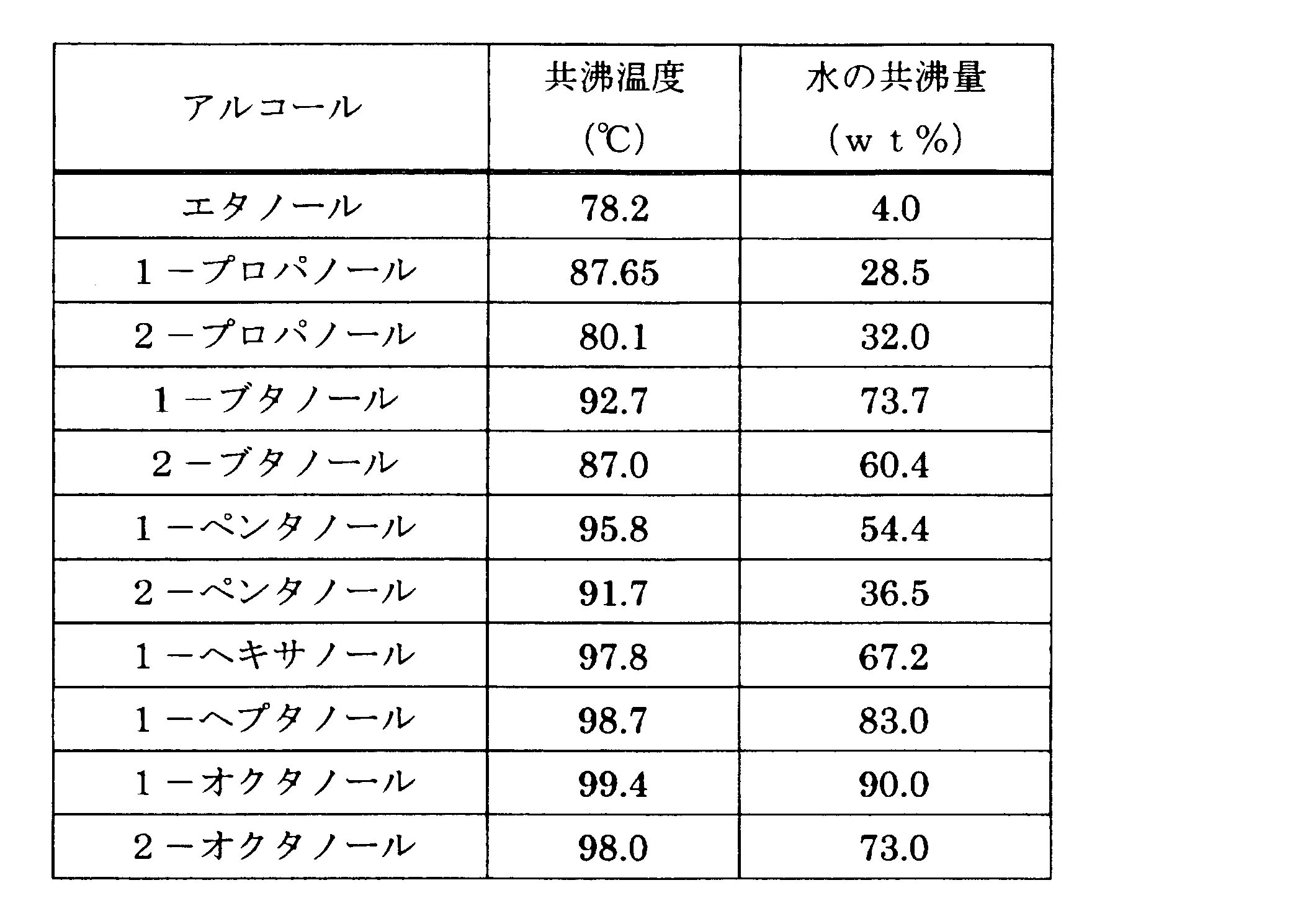
図1において、透明基板(ポリエチレン・ナフタレート)フィルム(厚み100μm)の上に透明導電膜(ITO)を厚み(150)nmで形成した。この導電膜付き透明基板を巻き取ってなるロール(1)から導電膜付き透明基板(2)を繰り出し、20~50nmのアナターゼ型酸化チタン、エタノールおよび水からなる酸化チタン含有ペーストをペースト塗布装置(3)から透明基板(2)の透明導電膜上に供給し、厚み(10)μmで塗布した。塗布後、塗膜を室温で10分間乾燥させ、さらに加熱器(4)で150℃で10分間焼成し、透明導電膜上に光触媒膜を形成した。
プロパノール浸漬および焼成による光触媒膜の脱水処理を行わなかった以外、実施例と同じ要領で操作を行って、電極を作製した。
図2に、実施例1で作製した透明電極を用いて構成した光電変換素子の例を示す。光電変換素子は、色素を吸着させた光触媒膜を備えた透明電極と、これに対向する対極と、両極間に配される電解質層とから主として構成されている。
電極として、比較例1で作製したものを用いた以外、参考例1と同様にして、光電変換素子を構成した。
(2) 透明基板
(3) ペースト塗布装置
(4),(6) 加熱器
(5) プロパノール
(7) 浸漬液
Claims (3)
- 透明基板上に透明導電膜を形成し、その上に光触媒膜を形成し、この光触媒膜に光増感色素を吸着させる電極の製造方法であって、光触媒膜への光増感色素の吸着の前に、透明基板の光触媒膜を、水との共沸温度が150℃以下のアルコールに浸漬し次いで加熱することで、水とアルコールの共沸により光触媒膜を脱水しておくことを特徴とする光電変換素子用電極の製造方法。
- アルコールが1-プロパノールまたは1-ブタノールであることを特徴とする請求項1記載の光電変換素子用電極の製造方法。
- 基板がフィルム又はシート状のものであり、光触媒膜の形成、光触媒膜の脱水、光触媒膜への光増感色素の吸着を連続的に行う請求項1または2記載の光電変換素子用電極の製造方法。
Priority Applications (3)
| Application Number | Priority Date | Filing Date | Title |
|---|---|---|---|
| PCT/JP2010/057145 WO2011132288A1 (ja) | 2010-04-22 | 2010-04-22 | 光電変換素子用電極の製造方法 |
| KR1020127030249A KR20130060195A (ko) | 2010-04-22 | 2010-04-22 | 광전 변환 소자용 전극의 제조방법 |
| CN2010800663368A CN102859786A (zh) | 2010-04-22 | 2010-04-22 | 光电转换元件用电极的制备方法 |
Applications Claiming Priority (1)
| Application Number | Priority Date | Filing Date | Title |
|---|---|---|---|
| PCT/JP2010/057145 WO2011132288A1 (ja) | 2010-04-22 | 2010-04-22 | 光電変換素子用電極の製造方法 |
Publications (1)
| Publication Number | Publication Date |
|---|---|
| WO2011132288A1 true WO2011132288A1 (ja) | 2011-10-27 |
Family
ID=44833844
Family Applications (1)
| Application Number | Title | Priority Date | Filing Date |
|---|---|---|---|
| PCT/JP2010/057145 Ceased WO2011132288A1 (ja) | 2010-04-22 | 2010-04-22 | 光電変換素子用電極の製造方法 |
Country Status (3)
| Country | Link |
|---|---|
| KR (1) | KR20130060195A (ja) |
| CN (1) | CN102859786A (ja) |
| WO (1) | WO2011132288A1 (ja) |
Cited By (1)
| Publication number | Priority date | Publication date | Assignee | Title |
|---|---|---|---|---|
| JP2013178929A (ja) * | 2012-02-28 | 2013-09-09 | Sekisui Chem Co Ltd | 色素増感太陽電池の製造方法及び電解質 |
Families Citing this family (1)
| Publication number | Priority date | Publication date | Assignee | Title |
|---|---|---|---|---|
| CN106471594A (zh) * | 2014-08-19 | 2017-03-01 | 积水化学工业株式会社 | 多孔质体的染色方法、光电极及光电模块 |
Citations (3)
| Publication number | Priority date | Publication date | Assignee | Title |
|---|---|---|---|---|
| JP2001076776A (ja) * | 1999-09-09 | 2001-03-23 | Tdk Corp | 色素増感型太陽電池 |
| JP2005251591A (ja) * | 2004-03-04 | 2005-09-15 | Toyo Seikan Kaisha Ltd | 色素増感型太陽電池における負極の製造方法 |
| JP2007242544A (ja) * | 2006-03-10 | 2007-09-20 | Sony Corp | 光電変換装置及びその製造方法、並びに金属酸化物多孔質層の表面処理液 |
Family Cites Families (2)
| Publication number | Priority date | Publication date | Assignee | Title |
|---|---|---|---|---|
| CN100340488C (zh) * | 2005-07-12 | 2007-10-03 | 武汉大学 | 一种制备高分散性掺锑氢氧化锡纳米微粉的方法 |
| CN101226966B (zh) * | 2008-01-22 | 2010-07-28 | 西安交通大学 | 染料敏化TiO2纳米晶太阳能电池的定制化导电薄膜及其制备 |
-
2010
- 2010-04-22 WO PCT/JP2010/057145 patent/WO2011132288A1/ja not_active Ceased
- 2010-04-22 CN CN2010800663368A patent/CN102859786A/zh active Pending
- 2010-04-22 KR KR1020127030249A patent/KR20130060195A/ko not_active Withdrawn
Patent Citations (3)
| Publication number | Priority date | Publication date | Assignee | Title |
|---|---|---|---|---|
| JP2001076776A (ja) * | 1999-09-09 | 2001-03-23 | Tdk Corp | 色素増感型太陽電池 |
| JP2005251591A (ja) * | 2004-03-04 | 2005-09-15 | Toyo Seikan Kaisha Ltd | 色素増感型太陽電池における負極の製造方法 |
| JP2007242544A (ja) * | 2006-03-10 | 2007-09-20 | Sony Corp | 光電変換装置及びその製造方法、並びに金属酸化物多孔質層の表面処理液 |
Cited By (1)
| Publication number | Priority date | Publication date | Assignee | Title |
|---|---|---|---|---|
| JP2013178929A (ja) * | 2012-02-28 | 2013-09-09 | Sekisui Chem Co Ltd | 色素増感太陽電池の製造方法及び電解質 |
Also Published As
| Publication number | Publication date |
|---|---|
| CN102859786A (zh) | 2013-01-02 |
| KR20130060195A (ko) | 2013-06-07 |
Similar Documents
| Publication | Publication Date | Title |
|---|---|---|
| JP4635473B2 (ja) | 光電変換素子の製造方法及び半導体電極の製造方法 | |
| JP2007194075A (ja) | 機能デバイス | |
| JP5070704B2 (ja) | 光電変換装置 | |
| JP2012059599A (ja) | カーボン系電極及び電気化学装置 | |
| WO2006095520A1 (ja) | 色素増感光電変換素子およびその製造方法ならびに電子装置およびその製造方法ならびに電子機器 | |
| US20120288978A1 (en) | Method for forming buffer layer in dye-sensitized solar cell | |
| JP2005158380A (ja) | 光電変換素子およびその製造方法ならびに電子装置およびその製造方法 | |
| US20120288977A1 (en) | Method for manufacturing dye-sensitized solar cell | |
| WO2011132288A1 (ja) | 光電変換素子用電極の製造方法 | |
| JP4963165B2 (ja) | 色素増感型太陽電池及び色素増感型太陽電池モジュール | |
| JP5452037B2 (ja) | 光電変換素子用電極の製造方法 | |
| JP5508730B2 (ja) | 透明電極上における光触媒膜の形成方法 | |
| JP5303298B2 (ja) | 透明電極上における光触媒膜の形成方法 | |
| JP2010205581A (ja) | 導電性メッシュを用いた光電変換素子の製造方法 | |
| KR20130051946A (ko) | 투명 전극 상에서의 광촉매막의 형성 방법 | |
| KR20120119073A (ko) | 염료 감응형 태양 전지의 제조 방법 | |
| JP5160045B2 (ja) | 光電変換素子 | |
| JP2007242544A (ja) | 光電変換装置及びその製造方法、並びに金属酸化物多孔質層の表面処理液 | |
| JP2010037138A (ja) | 酸化チタン膜の形成方法および光電変換素子 | |
| JP5530648B2 (ja) | 光電変換素子の製造方法 | |
| WO2011132287A1 (ja) | 透明電極上における光触媒膜の形成方法 | |
| JP2014063677A (ja) | 色素増感太陽電池における光触媒膜の形成方法、並びにその光触媒膜を具備した色素増感太陽電池およびその連続製造装置 | |
| KR101600786B1 (ko) | 염료감응형 태양전지 서브모듈의 제조방법 | |
| JP2012212539A (ja) | 色素増感太陽電池における対向電極の製造方法および色素増感太陽電池 | |
| WO2014041999A1 (ja) | 色素増感太陽電池における光触媒膜の形成方法 |
Legal Events
| Date | Code | Title | Description |
|---|---|---|---|
| WWE | Wipo information: entry into national phase |
Ref document number: 201080066336.8 Country of ref document: CN |
|
| 121 | Ep: the epo has been informed by wipo that ep was designated in this application |
Ref document number: 10850229 Country of ref document: EP Kind code of ref document: A1 |
|
| NENP | Non-entry into the national phase |
Ref country code: DE |
|
| ENP | Entry into the national phase |
Ref document number: 20127030249 Country of ref document: KR Kind code of ref document: A |
|
| 122 | Ep: pct application non-entry in european phase |
Ref document number: 10850229 Country of ref document: EP Kind code of ref document: A1 |
|
| NENP | Non-entry into the national phase |
Ref country code: JP |