WO2011122368A1 - 単結晶3C-SiC基板の製造方法およびそれによって得られた単結晶3C-SiC基板 - Google Patents
単結晶3C-SiC基板の製造方法およびそれによって得られた単結晶3C-SiC基板 Download PDFInfo
- Publication number
- WO2011122368A1 WO2011122368A1 PCT/JP2011/056518 JP2011056518W WO2011122368A1 WO 2011122368 A1 WO2011122368 A1 WO 2011122368A1 JP 2011056518 W JP2011056518 W JP 2011056518W WO 2011122368 A1 WO2011122368 A1 WO 2011122368A1
- Authority
- WO
- WIPO (PCT)
- Prior art keywords
- single crystal
- sic
- substrate
- growth
- layer
- Prior art date
Links
Images


Classifications
-
- C—CHEMISTRY; METALLURGY
- C30—CRYSTAL GROWTH
- C30B—SINGLE-CRYSTAL GROWTH; UNIDIRECTIONAL SOLIDIFICATION OF EUTECTIC MATERIAL OR UNIDIRECTIONAL DEMIXING OF EUTECTOID MATERIAL; REFINING BY ZONE-MELTING OF MATERIAL; PRODUCTION OF A HOMOGENEOUS POLYCRYSTALLINE MATERIAL WITH DEFINED STRUCTURE; SINGLE CRYSTALS OR HOMOGENEOUS POLYCRYSTALLINE MATERIAL WITH DEFINED STRUCTURE; AFTER-TREATMENT OF SINGLE CRYSTALS OR A HOMOGENEOUS POLYCRYSTALLINE MATERIAL WITH DEFINED STRUCTURE; APPARATUS THEREFOR
- C30B29/00—Single crystals or homogeneous polycrystalline material with defined structure characterised by the material or by their shape
- C30B29/10—Inorganic compounds or compositions
- C30B29/36—Carbides
-
- H—ELECTRICITY
- H01—ELECTRIC ELEMENTS
- H01L—SEMICONDUCTOR DEVICES NOT COVERED BY CLASS H10
- H01L21/00—Processes or apparatus adapted for the manufacture or treatment of semiconductor or solid state devices or of parts thereof
- H01L21/02—Manufacture or treatment of semiconductor devices or of parts thereof
- H01L21/02104—Forming layers
- H01L21/02365—Forming inorganic semiconducting materials on a substrate
- H01L21/02612—Formation types
- H01L21/02617—Deposition types
- H01L21/0262—Reduction or decomposition of gaseous compounds, e.g. CVD
-
- C—CHEMISTRY; METALLURGY
- C30—CRYSTAL GROWTH
- C30B—SINGLE-CRYSTAL GROWTH; UNIDIRECTIONAL SOLIDIFICATION OF EUTECTIC MATERIAL OR UNIDIRECTIONAL DEMIXING OF EUTECTOID MATERIAL; REFINING BY ZONE-MELTING OF MATERIAL; PRODUCTION OF A HOMOGENEOUS POLYCRYSTALLINE MATERIAL WITH DEFINED STRUCTURE; SINGLE CRYSTALS OR HOMOGENEOUS POLYCRYSTALLINE MATERIAL WITH DEFINED STRUCTURE; AFTER-TREATMENT OF SINGLE CRYSTALS OR A HOMOGENEOUS POLYCRYSTALLINE MATERIAL WITH DEFINED STRUCTURE; APPARATUS THEREFOR
- C30B25/00—Single-crystal growth by chemical reaction of reactive gases, e.g. chemical vapour-deposition growth
- C30B25/02—Epitaxial-layer growth
- C30B25/16—Controlling or regulating
-
- C—CHEMISTRY; METALLURGY
- C30—CRYSTAL GROWTH
- C30B—SINGLE-CRYSTAL GROWTH; UNIDIRECTIONAL SOLIDIFICATION OF EUTECTIC MATERIAL OR UNIDIRECTIONAL DEMIXING OF EUTECTOID MATERIAL; REFINING BY ZONE-MELTING OF MATERIAL; PRODUCTION OF A HOMOGENEOUS POLYCRYSTALLINE MATERIAL WITH DEFINED STRUCTURE; SINGLE CRYSTALS OR HOMOGENEOUS POLYCRYSTALLINE MATERIAL WITH DEFINED STRUCTURE; AFTER-TREATMENT OF SINGLE CRYSTALS OR A HOMOGENEOUS POLYCRYSTALLINE MATERIAL WITH DEFINED STRUCTURE; APPARATUS THEREFOR
- C30B25/00—Single-crystal growth by chemical reaction of reactive gases, e.g. chemical vapour-deposition growth
- C30B25/02—Epitaxial-layer growth
- C30B25/18—Epitaxial-layer growth characterised by the substrate
- C30B25/20—Epitaxial-layer growth characterised by the substrate the substrate being of the same materials as the epitaxial layer
-
- H—ELECTRICITY
- H01—ELECTRIC ELEMENTS
- H01L—SEMICONDUCTOR DEVICES NOT COVERED BY CLASS H10
- H01L21/00—Processes or apparatus adapted for the manufacture or treatment of semiconductor or solid state devices or of parts thereof
- H01L21/02—Manufacture or treatment of semiconductor devices or of parts thereof
- H01L21/02104—Forming layers
- H01L21/02365—Forming inorganic semiconducting materials on a substrate
- H01L21/02367—Substrates
- H01L21/0237—Materials
-
- H—ELECTRICITY
- H01—ELECTRIC ELEMENTS
- H01L—SEMICONDUCTOR DEVICES NOT COVERED BY CLASS H10
- H01L21/00—Processes or apparatus adapted for the manufacture or treatment of semiconductor or solid state devices or of parts thereof
- H01L21/02—Manufacture or treatment of semiconductor devices or of parts thereof
- H01L21/02104—Forming layers
- H01L21/02365—Forming inorganic semiconducting materials on a substrate
- H01L21/02436—Intermediate layers between substrates and deposited layers
- H01L21/02439—Materials
- H01L21/02441—Group 14 semiconducting materials
- H01L21/02447—Silicon carbide
-
- H—ELECTRICITY
- H01—ELECTRIC ELEMENTS
- H01L—SEMICONDUCTOR DEVICES NOT COVERED BY CLASS H10
- H01L21/00—Processes or apparatus adapted for the manufacture or treatment of semiconductor or solid state devices or of parts thereof
- H01L21/02—Manufacture or treatment of semiconductor devices or of parts thereof
- H01L21/02104—Forming layers
- H01L21/02365—Forming inorganic semiconducting materials on a substrate
- H01L21/02436—Intermediate layers between substrates and deposited layers
- H01L21/02494—Structure
-
- H—ELECTRICITY
- H01—ELECTRIC ELEMENTS
- H01L—SEMICONDUCTOR DEVICES NOT COVERED BY CLASS H10
- H01L21/00—Processes or apparatus adapted for the manufacture or treatment of semiconductor or solid state devices or of parts thereof
- H01L21/02—Manufacture or treatment of semiconductor devices or of parts thereof
- H01L21/02104—Forming layers
- H01L21/02365—Forming inorganic semiconducting materials on a substrate
- H01L21/02518—Deposited layers
- H01L21/02521—Materials
- H01L21/02524—Group 14 semiconducting materials
- H01L21/02529—Silicon carbide
-
- H—ELECTRICITY
- H01—ELECTRIC ELEMENTS
- H01L—SEMICONDUCTOR DEVICES NOT COVERED BY CLASS H10
- H01L21/00—Processes or apparatus adapted for the manufacture or treatment of semiconductor or solid state devices or of parts thereof
- H01L21/02—Manufacture or treatment of semiconductor devices or of parts thereof
- H01L21/02104—Forming layers
- H01L21/02365—Forming inorganic semiconducting materials on a substrate
- H01L21/02612—Formation types
- H01L21/02614—Transformation of metal, e.g. oxidation, nitridation
-
- H—ELECTRICITY
- H01—ELECTRIC ELEMENTS
- H01L—SEMICONDUCTOR DEVICES NOT COVERED BY CLASS H10
- H01L21/00—Processes or apparatus adapted for the manufacture or treatment of semiconductor or solid state devices or of parts thereof
- H01L21/02—Manufacture or treatment of semiconductor devices or of parts thereof
- H01L21/02104—Forming layers
- H01L21/02365—Forming inorganic semiconducting materials on a substrate
- H01L21/02656—Special treatments
- H01L21/02658—Pretreatments
- H01L21/02661—In-situ cleaning
-
- H—ELECTRICITY
- H01—ELECTRIC ELEMENTS
- H01L—SEMICONDUCTOR DEVICES NOT COVERED BY CLASS H10
- H01L21/00—Processes or apparatus adapted for the manufacture or treatment of semiconductor or solid state devices or of parts thereof
- H01L21/02—Manufacture or treatment of semiconductor devices or of parts thereof
- H01L21/04—Manufacture or treatment of semiconductor devices or of parts thereof the devices having at least one potential-jump barrier or surface barrier, e.g. PN junction, depletion layer or carrier concentration layer
- H01L21/18—Manufacture or treatment of semiconductor devices or of parts thereof the devices having at least one potential-jump barrier or surface barrier, e.g. PN junction, depletion layer or carrier concentration layer the devices having semiconductor bodies comprising elements of Group IV of the Periodic System or AIIIBV compounds with or without impurities, e.g. doping materials
- H01L21/20—Deposition of semiconductor materials on a substrate, e.g. epitaxial growth solid phase epitaxy
-
- Y—GENERAL TAGGING OF NEW TECHNOLOGICAL DEVELOPMENTS; GENERAL TAGGING OF CROSS-SECTIONAL TECHNOLOGIES SPANNING OVER SEVERAL SECTIONS OF THE IPC; TECHNICAL SUBJECTS COVERED BY FORMER USPC CROSS-REFERENCE ART COLLECTIONS [XRACs] AND DIGESTS
- Y10—TECHNICAL SUBJECTS COVERED BY FORMER USPC
- Y10T—TECHNICAL SUBJECTS COVERED BY FORMER US CLASSIFICATION
- Y10T428/00—Stock material or miscellaneous articles
- Y10T428/24—Structurally defined web or sheet [e.g., overall dimension, etc.]
- Y10T428/24355—Continuous and nonuniform or irregular surface on layer or component [e.g., roofing, etc.]
Definitions
- the present invention relates to a method of manufacturing a single crystal 3C (cubic system) -SiC substrate capable of significantly reducing surface defects and a single crystal 3C-SiC substrate obtained thereby.
- Single crystal SiC (silicon carbide) is noted as a next-generation semiconductor device material because it is superior in thermal and chemical stability to Si, has high mechanical strength, and is not easily damaged by radiation. Are collecting In addition, single crystal SiC can also be used as a base substrate for growing GaN because the lattice constant is close to that of GaN. Conventionally, as a method of obtaining single crystal SiC, a method of obtaining a SiC bulk substrate by sublimation method, and a method of heteroepitaxial growth of single crystal 3C-SiC on a Si substrate or an SOI substrate are performed.
- the epitaxial growth method on a Si substrate or SOI substrate is performed by carbonizing the Si substrate or SOI substrate to transform it into thin film SiC, and growing single crystal 3C-SiC using a silane gas and a hydrocarbon gas.
- Methods have been devised to suppress the amorphization and polycrystallization of SiC.
- the presence of defects in single crystal SiC lowers the performance of the semiconductor device, and causes the quality of the GaN layer to deteriorate even when used as a base substrate of the GaN layer. Therefore, a high quality single crystal SiC substrate with as few defects as possible is required.
- FIG. 1 is a diagram showing the relationship of the growth rate depending on temperature when the flow rate of reaction gas and the reaction pressure are generally the same in an epitaxial growth reaction.
- the horizontal axis is the reciprocal of the absolute temperature
- the right side of the drawing is the low temperature side
- the left side of the drawing is the high temperature side.
- the vertical axis is the epitaxial growth rate
- the lower side of the figure is the low speed side
- the upper side of the figure is the high speed side.
- the surface condition becomes rough, and again, it is not possible to obtain a quality suitable for manufacturing a semiconductor device. Therefore, by setting the flow rate condition of the supply gas and the film forming pressure constant and adjusting the film forming temperature up and down, it is possible to arbitrarily select the rate-limiting step of the film forming.
- the rate-determining step is from the reaction rate control to the transport rate control, and the desorption rate limit as in the case of increasing the film deposition temperature. It is also known to change into the above (Non-Patent Document 1).
- the rate-limiting step of the film formation by making the film formation temperature and the film formation pressure constant and adjusting the flow rate of the supplied gas up and down using this. Furthermore, in the 3C-SiC growth, when the film forming temperature and the flow rate condition of the supplied gas are made constant and the film forming pressure is lowered, the rate-limiting is the same as in the case of increasing the film forming temperature. It has been found that the stage changes from reaction-limited to transport-limited and then to desorption-limited. It is also possible to arbitrarily select the rate-limiting step of the film formation by making the film formation temperature and the flow rate condition of the supplied gas constant and adjusting the film formation pressure up and down using this.
- the above-described transport-limited area has to be used as a condition for epitaxial growth.
- surface roughness due to crystallinity does not occur as in the surface reaction-limited area, and although surface protrusions like the desorption-limited area do not occur, fine pits are formed on the surface. The problem of many defects being formed was inevitable.
- the present invention has been made in view of the above-described circumstances, and can significantly reduce surface defects generated in an epitaxial growth process, and can maintain the quality as a semiconductor device while simplifying the subsequent steps. It aims at provision of the manufacturing method of a SiC substrate, and the single crystal 3C-SiC substrate obtained by it.
- the method for producing a single crystal 3C-SiC substrate of the present invention is a method for producing a single crystal 3C-SiC substrate in which a single crystal 3C-SiC layer is formed on a base substrate by epitaxial growth.
- the gist is to perform the second growth step of further epitaxially growing the single crystal 3C-SiC layer obtained in the first growth step so as to fill the surface pits.
- a single crystal 3C-SiC substrate of the present invention is a single crystal 3C-SiC substrate in which a single crystal 3C-SiC layer is formed by epitaxial growth on a base substrate, and a single crystal 3C-SiC layer
- the gist of the present invention is that the number of defects due to surface pits present on the surface of the semiconductor device is 8 ⁇ 10 6 / cm 2 or less immediately after the epitaxial growth.
- the first single crystal 3C-SiC layer is epitaxially grown to have a surface state in which surface pits are formed in the surface with high flatness.
- a growth step and a second growth step of further epitaxially growing the single crystal 3C-SiC layer obtained in the first growth step so as to fill the surface pits on the surface are performed.
- surface pits are formed in the first growth stage, a portion other than the surface pits forms a single crystal 3C-SiC layer of the surface property which secures flatness, and in the second growth stage, the surface is formed.
- the number of defects due to surface pits present on the surface of the single crystal 3C-SiC layer is 8 ⁇ 10 6 / cm 2 or less immediately after epitaxial growth.
- the post-process is simplified, the cost is reduced accordingly, and the factors affecting quality are reduced, quality stability and It is advantageous also in terms of yield etc., and the quality can be secured as the application of semiconductor devices etc.
- the first growth step is epitaxial growth in a transport-limited area
- the second growth step in the case of epitaxial growth in the desorption-limited region, In the transport-limited area, abnormal growth of crystal nuclei causing defects is suppressed, and a single crystal 3C-SiC layer with good surface crystallinity and good crystallinity can be stably obtained at a high growth rate with surface pits scattered in a flat surface. be able to.
- single crystal 3C-SiC is grown so that the surface pits formed by transport limited growth are filled instead of conventional growth of protrusions, and the flatness of the flat surface is also maintained. Ru.
- the present invention when switching from the first growth stage to the second growth stage is performed by at least one of reduction of the flow rate of the source gas, reduction of the film forming pressure, and increase of the substrate temperature, By switching from the first growth stage to the second growth stage by reducing the flow rate of the source gas, it is possible to quickly switch only by reducing the flow rate without changing the pressure or temperature which takes a relatively long time for setting change. It can be performed.
- the switching from the first growth stage to the second growth stage is performed by reducing the film forming pressure, so that the temperature change which takes a relatively long time for the setting change can be performed only by reducing the pressure without changing the temperature. it can. Further, since the flow rate of the source gas is not changed, the atmosphere for performing the epitaxial growth is more stable, and the growth of the single crystal 3C-SiC layer is stably performed. By switching from the first growth step to the second growth step by raising the substrate temperature, the flow rate of the source gas is not changed, so the atmosphere for performing epitaxial growth becomes more stable, and single crystal 3C-SiC layer Growth is stable.
- the Si in the present invention in the case of using a base substrate composed of a semiconductor crystal at least the surface layer of which contains Si, Single crystal 3C with good crystallinity and sufficient quality as a semiconductor device by forming a single crystal 3C-SiC layer with good crystallinity and significantly reduced surface defects with respect to a base substrate consisting of a semiconductor crystal containing at least the surface layer of Si.
- the SiC substrate can be manufactured inexpensively.
- using the base substrate in which at least the surface layer portion is made of Si the Si in the surface layer portion of the base substrate is carbonized to transform it into a SiC layer, and the SiC layer is used as a seed layer.
- a single-crystal 3C-SiC substrate is obtained which has a good crystallinity and significantly reduced surface defects with respect to a base substrate of which at least the surface layer is made of Si, and secures the quality as a semiconductor device. Can be manufactured.
- the thickness of the single crystal 3C-SiC layer formed in the first growth step is 500 nm or more, and the thickness of the single crystal 3C-SiC layer formed in the second growth step is 500 nm or more. If the thickness of the single crystal 3C-SiC layer formed in the first growth step is less than 500 nm, 3C-SiC is not sufficiently formed in the portion of the surface pits formed to be scattered in the flat surface. As a result, the base substrate is exposed, and even after the subsequent second growth step, the surface pits can not be filled with 3C-SiC.
- the thickness of the single crystal 3C-SiC layer formed in the first growth step is set to 500 nm or more, surface pits are buried in the subsequent second growth step to eliminate defects and ensure flatness.
- a single crystal 3C-SiC layer with few defects can be obtained. If the thickness of the single crystal 3C-SiC layer formed in the second growth step is less than 500 nm, the surface pits formed to be scattered in the flat surface in the first growth step in the second growth step It can not be filled enough. Therefore, by setting the thickness of the single crystal 3C-SiC layer formed in the second growth step to 500 nm or more, the surface pits formed in the first growth step are filled to eliminate defects and ensure flatness.
- the thickness of the single crystal 3C-SiC layer formed in the first growth step is 900 to 2900 nm
- the thickness of the single crystal 3C-SiC layer formed in the second growth step is 700 to 3700 nm
- a single crystal 3C—SiC layer can be formed so that surface pits that can disappear in the second growth stage are scattered in a sufficiently flat surface, and single crystal with few defects while securing flatness A 3C-SiC layer is obtained.
- the surface pits formed in the first growth step are buried to eliminate defects, and a single crystal 3C-SiC layer with few defects is obtained while securing flatness.
- the main component of the raw material gas in forming a single crystal 3C-SiC layer by epitaxial growth on the base substrate is monomethylsilane
- Monomethylsilane is a gas with little risk of explosion, etc., and is extremely excellent in that there is less risk when operating the gas supply valve, operating the exhaust valve, or operating the heater output during film formation.
- the substrate temperature is 970 ° C. or more and 1120 ° C.
- the flow rate of monomethylsilane per wafer contained in the raw material gas is 1.0 sccm or more and 30.0 sccm or less, and the film forming pressure Is more than 9 ⁇ 10 ⁇ 6 Torr and not more than 4 ⁇ 10 ⁇ 1 Torr,
- the flow rate of monomethylsilane per wafer contained in the raw material gas is 6.0 sccm or less, the substrate temperature is 1100 ° C. or more, and less than the melting point of the base substrate, and the deposition pressure is 1 ⁇ 10 ⁇ 7.
- the flow rate of monomethylsilane per wafer is 2.0 sccm or more and 10.0 sccm or less, and the film forming pressure is 3 ⁇ 10 ⁇ 5 Torr or more 1 ⁇ 10 -1 Torr or less,
- the flow rate of monomethylsilane per wafer is 3.0 sccm or less, The growth efficiency of epitaxial growth can be secured, and a single crystal 3C-SiC layer with significantly reduced surface defects can be produced with high productivity.
- the deposition pressure is 1 ⁇ 10 ⁇ 4 Torr or less.
- the deposition pressure is 1 ⁇ 10 ⁇ 1 Torr or higher.
- the switching from the first growth stage to the second growth stage is performed at least by reducing the film forming pressure, The growth efficiency of epitaxial growth can be secured, and a single crystal 3C-SiC layer with significantly reduced surface defects can be produced with high productivity.
- transport-limited A substrate temperature range where a deposition rate of 90% or more of the maximum deposition rate obtained in epitaxial growth under the same conditions of source gas, atmosphere, flow rate, and pressure is obtained.
- Desorption rate limiting Of the substrate temperature range where a deposition rate of less than 90% of the maximum deposition rate obtained in epitaxial growth under the same conditions of source gas, atmosphere, flow rate, and pressure is obtained, higher temperature side than transport limited Substrate temperature range. Reaction-limited: A substrate at a temperature lower than transport-limited in a substrate temperature range where a deposition rate of less than 90% of the maximum deposition rate obtained in epitaxial growth under the same conditions of source gas, atmosphere, flow rate and pressure is obtained. Temperature range.
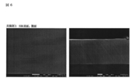
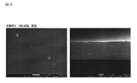
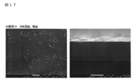
- Example 1 surface, cross-sectional SEM photograph.
- Example 2 surface, cross-sectional SEM photograph.
- Example 3 Surface, cross-sectional SEM photograph.
- Example 4 Surface, cross-sectional SEM photograph.
- Example 5 Surface, cross-sectional SEM photograph.
- Example 6 surface, cross-sectional SEM photograph.
- Example 7 Surface, cross-sectional SEM photograph.
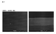
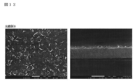
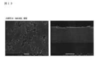
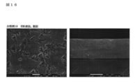
- Comparative Example 8 Surface, cross-sectional SEM photograph. Comparative example 9 surface, cross section SEM photograph. Comparative example 10 Surface, cross-sectional SEM photograph.
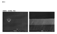
- Comparative example 11 Surface, cross-sectional SEM photograph. Comparative example 12 surface, cross-sectional SEM photograph. Comparative example 13 Surface, cross-sectional SEM photograph. Comparative example 14 Surface, cross-sectional SEM photograph. Comparative example 15 Surface, cross-sectional SEM photograph. Comparative example 16 surface, section SEM photograph. Example 17 surface, sectional SEM photograph. Example 18 Surface, cross-sectional SEM photograph. Example 19 surface, sectional SEM photograph. It is a calibration curve which shows change of processing chamber pressure to source gas flow rate.
- FIG. 2 is a process diagram showing an embodiment of a method of manufacturing a single crystal 3C-SiC substrate according to the present invention.
- a single-crystal 3C-C is prepared by preparing a base substrate as a base for forming a single-crystal 3C-SiC layer by epitaxial growth, and forming a single-crystal 3C-SiC layer by epitaxial growth on the base substrate. It is a manufacturing method of a SiC substrate.
- the epitaxial growth is performed by epitaxially growing the single crystal 3C—SiC layer into a surface state consisting of a surface having high flatness and surface pits scattered therein;
- the single crystal 3C-SiC layer obtained in the first growth step is further epitaxially grown to fill the surface pits on the surface, and a second growth step is performed.
- the base substrate is not particularly limited as long as the 3C-SiC layer can be formed by epitaxial growth, and various substrates can be used. In the present invention, when a single crystal Si substrate or an SOI substrate is used as the base substrate, particularly great effects can be obtained.
- a MgO substrate, a hexagonal SiC bulk substrate by sublimation, a BP substrate, a sapphire substrate, a 3C-SiC free-standing substrate, a GaN substrate, a GaAs substrate, an AlN substrate, an InN substrate, a SiGe substrate, a SiGe on Insulator substrate etc. are used as a base substrate. Even when used, the effects of the present invention can be obtained.
- the substrate surface is cleaned by appropriately combining known cleaning such as cleaning, ultrasonic acetone cleaning, ultrasonic methanol cleaning and the like.
- the surface oxide film is removed.
- the above-mentioned cleaning step is usually unnecessary, but it may be performed as needed. Good.
- a vacuum of a substrate temperature of 1000 ° C. or more and a pressure of less than 1 Torr in an epitaxial growth furnace for example, a vacuum of a substrate temperature of 1000 ° C. or more and a pressure of less than 1 Torr in an epitaxial growth furnace. Anneal for about 10 minutes in an atmosphere. Alternatively, for example, annealing is performed for about 10 minutes in a hydrogen atmosphere under normal pressure or reduced pressure at a substrate temperature of 1000 ° C. or higher.
- the adjustment process of the base substrate is completed, and the first film forming process is subsequently performed in the epitaxial growth furnace.
- the substrate temperature is 1000 in the epitaxial growth furnace.
- Anneal for about 10 minutes in a vacuum atmosphere at a temperature of 1 ° C. or higher and a pressure of less than 1 Torr.
- annealing is performed for about 10 minutes in a hydrogen atmosphere under normal pressure or reduced pressure at a substrate temperature of 1100 ° C. or higher.
- the adjustment process of the base substrate may be completed, and the first film forming process may be performed in the epitaxial growth furnace.
- the substrate temperature is about 6 to 40 nm on the surface of the base substrate in a silane gas atmosphere or a mixed atmosphere of silane gas and hydrogen at a substrate temperature of 700 ° C. or more, less than the melting point of the base substrate, normal pressure or reduced pressure.
- a single crystal silicon layer is grown.
- the single crystal silicon layer formed on the surface of the substrate is transformed into a single crystal 3C-SiC layer by the same process as in the case of using an SOI substrate described later.
- the adjustment process of the base substrate is completed, and the first film forming process is subsequently performed in the epitaxial growth furnace.
- a semiconductor substrate in which at least a surface layer portion of Si substrate, SOI substrate, SiGe substrate, SiGe on Insulator substrate, etc. is made of Si or whose main component is Si is used as the base substrate
- a semiconductor crystal containing Si or Si as a main component is carbonized to be transformed into a 3C-SiC layer, and the epitaxial growth is performed in the first and second growth stages using the 3C-SiC layer as a seed layer.
- a single crystal 3C-SiC layer is formed which has good crystallinity and significantly reduced surface defects with respect to a base substrate of which at least the surface layer is made of Si, thereby securing the quality as a semiconductor device.
- a crystalline 3C-SiC substrate can be manufactured inexpensively. More specifically, a Si substrate or an SOI substrate can be used as a base substrate of which at least the surface layer portion is made of Si.
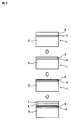
- FIG. 3 is a diagram for explaining a process of adjusting a base substrate when an SOI substrate is used as the base substrate. First, an SOI substrate 1 having a surface Si layer 3 of a predetermined thickness and a buried insulating layer 4 is prepared. Then, the thickness of the surface Si layer 3 of the SOI substrate 1 is reduced to a predetermined thickness of 6 nm or more according to the target substrate structure. Note that this thinning step may not be performed.
- the SOI substrate 1 is heated in a hydrocarbon gas atmosphere to transform the surface Si layer 3 into a single crystal 3C—SiC layer 5. Then, an epitaxial growth step is performed using the single crystal 3C-SiC layer 5 as the seed layer 5.
- an SiO 2 layer of a predetermined thickness is formed as the embedded insulating layer 4 in the vicinity of the surface of the Si base material 2, and a surface Si layer 3 of a predetermined thickness is formed on the surface.
- the thickness of the buried insulating layer 4 is set to be about 1 to 200 nm.
- the thickness of the surface Si layer 3 of the SOI substrate 1 is reduced to a predetermined thickness of 6 nm or more according to the target substrate structure.
- This thinning is performed, for example, by heating the SOI substrate 1 in an oxidizing atmosphere to leave a predetermined thickness of Si layer in the vicinity of the interface with the buried insulating layer 4 by a predetermined depth from the surface of the surface Si layer 3. After oxidation, the oxide layer formed on the surface is removed by etching with hydrofluoric acid or the like. Note that this thinning step may not be performed.
- the thickness of the thinned surface Si layer 3 is preferably 6 nm or more. It is practically difficult to make the thickness of the thinned surface Si layer 3 less than 6 nm over the entire surface of the base substrate having a diameter of 2 inches or more, leading to a defect of the surface Si layer 3 in part of the substrate.
- the SOI substrate 1 is heated in a hydrocarbon gas atmosphere to transform the surface Si layer 3 into a single crystal 3C—SiC layer 5.
- the transformation step can be performed, for example, in a heating furnace capable of atmosphere control, by controlling the temperature while switching the atmosphere gas (hydrogen gas and hydrocarbon gas) introduced into the heating furnace.
- the SOI substrate 1 is installed in a heating furnace, and while the mixed gas of hydrogen gas and hydrocarbon gas is supplied into the heating furnace, the ambient temperature in the heating furnace is raised.
- the surface Si layer 3 of the SOI substrate 1 is transformed into a single crystal 3C-SiC layer 5.
- the SOI substrate 1 is placed in a heating furnace, and a mixed gas in which a hydrocarbon-based gas is mixed at a ratio of 1% by volume to hydrogen gas is supplied into the heating furnace.
- a mixed gas in which a hydrocarbon-based gas is mixed at a ratio of 1% by volume to hydrogen gas is supplied into the heating furnace.
- the atmosphere temperature in the heating furnace is heated to 1100 to 1405.degree. It is more preferably heated to 1150 to 1300 ° C.
- the surface Si layer 3 of the SOI substrate 1 is transformed into the single crystal 3C—SiC layer 5.
- the hydrogen gas is a carrier gas, and for example, propane gas can be used as the hydrocarbon gas.
- the thickness of the single crystal 3C-SiC layer 5 formed by the above transformation step is preferably set to about 3 nm to 20 nm in order to reduce defect defects in the same layer and to suppress deterioration of crystallinity due to three-dimensional growth. It is more preferably 4 to 10 nm, and even more preferably about 5 to 7 nm.
- the thickness of the transformed single crystal 3C-SiC layer 5 exceeds 20 nm, the upper part of the single crystal 3C-SiC layer 5 locally causes nuclear growth to form grain agglomerates, and the surface condition becomes rough, which is not preferable. It becomes a state. Therefore, in order to prevent deterioration of the quality of the single crystal 3C-SiC film due to the epitaxial growth after the metamorphosis due to the effect of the surface roughness, it is essential to set the thickness of the single crystal 3C-SiC layer 5 to 20 nm or less It is more preferably 10 nm or less, and still more preferably 7 nm or less.
- the thickness of the transformed single crystal 3C-SiC layer 5 is set to 3 nm, the single crystal 3C-SiC layer 5 is sublimated in the initial stage of epitaxial growth of the single crystal SiC layer 5 after the transformation treatment . Therefore, in order to prevent the quality of the single crystal 3C-SiC film from being degraded due to the epitaxial growth after the metamorphosis due to the influence of the sublimation, it is essential to set the thickness of the single crystal 3C-SiC layer 5 to 3 nm or more. 4 nm or more is more preferable, and 5 nm or more is more preferable.
- a single crystal 3C-SiC layer is grown on the seed layer by epitaxially growing the single crystal 3C-SiC layer 5 on the SOI substrate 1 subjected to the carbonization treatment as the seed layer.
- a single crystal 3C-SiC layer to be a seed layer is formed in the surface layer portion, and It is also possible to grow a single crystal 3C-SiC layer by epitaxial growth.
- the base substrate on which the single crystal 3C-SiC layer 5 is formed is disposed in the processing chamber, and the source gas containing monomethylsilane gas is flowed in the processing chamber at a predetermined flow rate (for example, about 1 sccm).
- a predetermined flow rate for example, about 1 sccm.
- the surface having high flatness is a smooth surface excluding surface pits in the surface of the single crystal 3C-SiC layer obtained by epitaxial growth, and is a gentle surface of 10 ° or less with respect to the least square plane of the substrate surface. It is a purport that you may include the undulation comprised by the various inclination.
- the above-mentioned least squares plane is used as a reference plane obtained by performing atomic force microscope (AFM) measurement on a single crystal 3C-SiC surface and performing least squares fitting on the obtained surface shape data.
- AFM measurement is performed in the range of 1 to 50 ⁇ m square.
- the first single crystal 3C-SiC layer 6 is formed on the seed layer 5
- the second single crystal 3C-SiC layer 7 is further formed.
- epitaxial growth is performed in a transport-limited region in epitaxial growth
- epitaxial growth is performed in a desorption-limited region in epitaxial growth. More specifically, as described with reference to FIG.
- the growth rate has a temperature-dependent relationship. That is, in the epitaxial growth, if the flow rate and pressure conditions are constant, the temperature in the surface reaction limited area where the growth rate becomes rapidly faster as the temperature rises in the low temperature area and the temperature on the higher temperature side than the area Growth rate decreases sharply with temperature rise in the transport-limited area where the growth rate increase with the increase is extremely small (in other words, less temperature-dependent) and on the higher temperature side than the transport-limited area There is a rate-limiting area. In the above-described surface reaction-limited region, the chemical reaction rate governs the growth rate.
- the surface condition becomes rough, and again, it is not possible to obtain a quality suitable for manufacturing a semiconductor device. Therefore, as described above, conventionally, when manufacturing a single crystal 3C-SiC substrate as a base device for semiconductor devices or GaN, it is necessary to use only the above-described transport-limited region as a condition for epitaxial growth. However, in the above transport-limited area, surface roughness due to crystallinity does not occur as in the surface reaction-limited area, and surface protrusions such as the desorption-limited area do not occur, but the surface is minute A large number of surface pits were formed, and surface defects due to the surface pits were unavoidable.
- the inventors have confirmed that epitaxial growth can not be sufficiently performed to reduce surface pits simply by raising the substrate temperature stepwise from conventional low temperature to high temperature. Then, intensive studies were conducted on the existence of a special condition setting of epitaxial growth that reduces surface pits generated on the surface in the process of single crystal 3C-SiC layer growth. In the process, repeated tests were conducted based on the idea that surface pits could be reduced by combining epitaxial growth, which was conventionally performed only in the transport-limited area, with epitaxial growth in other controlled areas. .
- the planar shape of the surface pits formed in the first growth step is determined by the relationship between the crystal structure of the single crystal 3C-SiC layer to be grown and the crystal plane (ie, crystal orientation) disposed on the surface.
- the main surface orientation of single crystal 3C-SiC to be grown is (111)
- surface pits having a triangular shape in plan view are formed.
- the main surface orientation of the grown single crystal 3C-SiC is (100)
- surface pits having a square shape in plan view are formed.
- the thickness of the single crystal 3C-SiC layer formed in the first growth step is preferably 500 nm or more, and the thickness of the single crystal 3C-SiC layer formed in the second growth step is 500 nm or more Is preferred. That is, if the thickness of the single crystal 3C—SiC layer formed in the first growth step is less than 500 nm, 3C— in the portion of the surface pits formed so as to be scattered in the highly flat surface. Since the base substrate is exposed without forming SiC, the surface pits can not be filled with 3C-SiC even after the subsequent second growth step.
- the thickness of the single crystal 3C-SiC layer formed in the first growth step is set to 500 nm or more, surface pits are buried in the subsequent second growth step to eliminate defects and ensure flatness.
- a single crystal 3C-SiC layer with few defects can be obtained.
- the thickness of the single crystal 3C-SiC layer formed in the second growth step is less than 500 nm, the surface pits formed to be scattered in the highly flat surface in the first growth step are It will not be possible to fully fill in the growth phase of 2. Therefore, by setting the thickness of the single crystal 3C-SiC layer formed in the second growth step to 500 nm or more, the surface pits formed in the first growth step are filled to eliminate defects and ensure flatness.
- a single crystal 3C-SiC layer with few defects can be obtained.
- the main surface orientation of single crystal 3C-SiC to be grown is (111)
- a surface pit having a triangular shape in plan view is formed, and a 3C-SiC layer having a sufficient surface flatness is formed with a thickness of less than 500 nm. It tends not to be possible to sufficiently fill the surface pits in the second growth stage.
- the thickness of the single crystal 3C-SiC layer formed in the first growth step is preferably 900 to 2900 nm, and the thickness of the single crystal 3C-SiC layer formed in the second growth step is 700 to 3700 nm It is preferable to That is, in the first growth stage, a single crystal 3C-SiC layer can be formed so that surface pits that can disappear in the second growth stage are scattered in a surface with high enough flatness, and the height of the flatness can be increased. While securing, a single crystal 3C-SiC layer with few defects is obtained.
- the surface pits formed in the first growth step are buried to eliminate defects, and a single crystal 3C-SiC layer with few defects is obtained while securing the height of flatness.
- epitaxial growth may be performed in the above-described transport-limited region. In order to epitaxially grow in the transport-limited area as the first growth stage, it is not intended to limit various conditions including the source gas, atmosphere, flow rate, pressure, temperature, etc., but the treatment under the following conditions is generally adopted can do.
- Atmosphere Raw material gas whose main component is monomethylsilane Substrate temperature: 970 to 1120 ° C.
- Flow rate 1.0 to 30.0 sccm (flow rate of monomethylsilane per wafer contained in the above source gas)
- Pressure 1 ⁇ 10 ⁇ 4 to 4 ⁇ 10 ⁇ 1 Torr
- the pressure conditions after calibration according to FIG. 24 described later have the following values.
- Pressure 9 ⁇ 10 ⁇ 6 to 4 ⁇ 10 ⁇ 1 Torr
- the second growth step is not intended to limit various conditions including the source gas, atmosphere, flow rate, pressure, and temperature, as long as epitaxial growth can be performed in the above-described desorption-limited region. In order to epitaxially grow in the desorption-limited area as the growth stage, the process under the following conditions can be employed.
- Atmosphere Raw material gas whose main component is monomethylsilane Substrate temperature: 1100 ° C. or more and below melting point of base substrate Flow rate: 0.1 to 6.0 sccm (flow rate of monomethylsilane per wafer contained in the above raw material gas) Pressure: 1 ⁇ 10 ⁇ 5 to 5 ⁇ 10 ⁇ 4 Torr
- Pressure 1 ⁇ 10 ⁇ 7 to 6 ⁇ 10 ⁇ 5 Torr
- the lower limit value of the film forming pressure 1 ⁇ 10 ⁇ 5 Torr (1 ⁇ 10 ⁇ 7 Torr after calibration described later), is the maximum capacity of the turbo molecular pump for exhausting the growth chamber used in the experiment.
- the effect of the present invention can be obtained even when the film formation is performed in the desorption controlled area where the film formation pressure is lowered.
- monomethylsilane is a gas that is less likely to cause an explosion, and particularly, as in the present invention, it is necessary to operate the gas supply valve, operate the exhaust valve, or operate the heater output during film formation.
- the membrane is extremely excellent in that the risk is small.
- the SiC quality improvement effect itself of the present invention can be similarly obtained when other source gases such as silane gas and propane gas are used.
- the thickness of the single crystal 3C-SiC to be epitaxially grown can be adjusted by the length of the processing time. The switching from the first growth stage to the second growth stage can be performed by reducing the source gas flow rate, reducing the deposition pressure, and / or raising the substrate temperature, and simply low temperature growth as in the prior art.
- the film forming pressure is lowered, and the transport limitation in the first growth stage is eliminated from the second growth stage. It is also possible to switch to rate-limiting.
- switching from the first growth step to the second growth step is performed by lowering the film forming pressure, so that the temperature change that takes a relatively long time for setting change is not changed, and switching is performed only by reducing the pressure. It can be performed.
- the flow rate of the source gas is not changed, the atmosphere for performing the epitaxial growth is more stable, and the growth of the single crystal 3C-SiC layer is stably performed.
- the transport limitation in the first growth stage to the desorption rate limitation in the second growth stage by keeping the composition of the source gas or the composition and mixing ratio of the source gas and the carrier gas, the flow rate, and the pressure constant, and raising the substrate temperature, the transport limitation in the first growth stage to the desorption rate limitation in the second growth stage.
- the switching from the transport limited in the first stage to the desorption limited in the second stage may be performed by combining the flow rate change of the source gas, the change of the film forming pressure, and the change of the substrate temperature.
- a single crystal 3C-SiC layer is formed by epitaxial growth on the base substrate, and the number of surface pit defects present on the surface of the single crystal 3C-SiC layer is epitaxially grown. In the state immediately after, it can be 8 ⁇ 10 6 / cm 2 or less. For this reason, since there are few surface pit defects generated on the surface of the single crystal 3C-SiC layer in the process of epitaxial growth, the post-process is simplified, the cost is reduced by that amount, the factors affecting the quality are reduced, quality stability and yield It is advantageous also in terms of etc., and the quality can be secured as the application of semiconductor devices etc.
- another semiconductor film such as a GaN layer is further formed by epitaxial growth on the single crystal 3C-SiC layer formed by epitaxial growth. That is, for example, a single crystal 3C-SiC substrate obtained by epitaxial growth is disposed in a processing chamber, ammonia gas is supplied into the processing chamber at a gas flow rate of about 100 to 10000 sccm, and organic such as triethylgallium or trimethylgallium By processing at a temperature of 800 to 1405 ° C.
- the single crystal 3C-SiC layer has a surface state including a surface with high flatness and surface pits scattered therein.
- a first growth step of forming and a second growth step of further epitaxially growing the single crystal 3C-SiC layer obtained in the first growth step so as to fill the surface pits are performed.
- an apparatus capable of epitaxially growing one base substrate per processing was used in the above epitaxial growth.
- the present invention is not limited to such a single wafer type epitaxial device.
- Table 1 below is a list of processing conditions under which the single crystal 3C-SiC layer is grown by epitaxial growth for the base substrate prepared as described above.
- the SOI substrate is used as the base substrate, the pressure condition and the flow rate of monomethylsilane per wafer are made constant, and the temperature condition is changed to perform the first growth step (transport limited) ⁇ second growth step. They are epitaxially grown by switching (desorption-limited rate).
- the SOI substrate is used as the base substrate, the pressure condition is kept constant, and the temperature condition and the flow rate of monomethylsilane per wafer are changed to perform the first growth step (transport limited) ⁇ the second growth step (desorption)
- the epitaxial growth is performed by switching the switching rate.
- the Si substrate is used as the base substrate, the pressure condition and the flow rate of monomethylsilane per wafer are made constant, and the temperature condition is changed to perform the first growth step (transport limited) ⁇ second growth step. They are epitaxially grown by switching (desorption-limited rate).
- the Si substrate is used as the base substrate, the pressure condition is kept constant, and the temperature condition and the flow rate of monomethylsilane per wafer are changed to perform the first growth step (transport limited) ⁇ the second growth step (desorption)
- the epitaxial growth is performed by switching the switching rate.
- Example 17 uses an SOI substrate as a base substrate, constant temperature conditions, and 5 ⁇ 10 -4 to 9 ⁇ 10 -4 Torr pressure conditions (3 ⁇ 10 -5 to 1 ⁇ 10 -4 Torr after calibration described later) And the first growth stage (transport-limited) ⁇ the second growth stage (desorption-limited) by changing the flow rate of monomethylsilane per wafer, and making epitaxial growth. It is.
- Example 18 uses the SOI substrate as a base substrate, keeps the temperature conditions constant, changes the pressure and the flow rate of monomethylsilane per wafer, and performs the first growth step (transport limited) ⁇ second growth step (desorption) The epitaxial growth is performed by switching the rate-limiting).
- Example 19 is based on a Si substrate, and the pressure condition is substantially constant at 2 ⁇ 10 ⁇ 4 to 5 ⁇ 10 ⁇ 4 Torr (which is 1 ⁇ 10 ⁇ 5 to 3 ⁇ 10 ⁇ 5 Torr after calibration described later). Then, by changing the temperature condition and the flow rate of monomethylsilane per wafer, the first growth stage (transport limited) ⁇ the second growth stage (desorption limited) is switched to perform epitaxial growth.
- the film forming pressure is 9 ⁇ 10 ⁇ 4 Torr (1 ⁇ 10 ⁇ 4 Torr after calibration described later) or less
- the first growth step to the second growth Switching to the stage was performed by reducing the flow rate of the source gas and / or raising the substrate temperature.
- the film formation pressure is 1 ⁇ 10 ⁇ 1 Torr or more
- switching from the first growth step to the second growth step is performed by at least reducing the film formation pressure.
- the rate-limiting step was determined as follows. That is, the source gas, atmosphere, flow rate, pressure and temperature were fixed on the 3C-SiC seed layer to grow a 3C-SiC epitaxial layer about 1 ⁇ m thick.
- the source gas, atmosphere, flow rate, and pressure are the conditions used in the first growth stage and the second growth stage described in the Examples and Comparative Examples, respectively, and grown at various substrate temperatures every 10 to 50 ° C. Did. Then, for each film forming condition, the average growth rate was calculated by dividing the thickness of the SiC layer by the holding time.
- the substrate temperature calibration curves of the substrate temperature and the heater temperature were obtained in advance using a substrate with a thermocouple or the like, and each growth condition was determined from the heater temperature at the time of growth using the above calibration curve. From the data of the average growth rate and the substrate temperature obtained, a curve for determining the rate-limiting step as shown in FIG. 1 was created.
- Comparative Example 8 is obtained by performing epitaxial growth only in the first step of transport limitation. In Comparative Example 9, epitaxial growth was performed only in the first step of desorption limited rate. Comparative Example 10 is obtained by epitaxially growing the first step in a reaction-limited manner and the second step in a desorption-limited manner.
- Comparative Example 11 is obtained by epitaxially growing the first step in the transport-limited manner by changing the flow rate of monomethylsilane after epitaxially growing the transport-limited in the first step.
- Comparative Example 12 epitaxial growth is performed with the first stage being rate-limited and the second stage being transport-limited, and the thickness of the single crystal 3C-SiC layer after the first stage is less than 500 nm.
- Comparative Example 13 epitaxial growth was performed under high pressure conditions only in the first step of transport limitation.
- epitaxial growth is performed with the first step being rate-limited and the second step being transport-limited, and the thickness of the single crystal 3C-SiC layer after the end of the first step is less than 500 nm.
- the comparative example 15 and the comparative example 16 are epitaxially grown only at the desorption rate limit.
- the film forming pressure in Table 1 above is a reading by a Baratron vacuum gauge, and it seems that the accuracy reliability is not so high, and the tendency is particularly strong on the low pressure side. Therefore, a calibration curve was obtained for the deposition pressure, and the value was calibrated.
- the calibration curve measures the pressure at the outlet of the processing chamber when the source gas is supplied at each flow rate into the processing chamber at a predetermined temperature of 950 ° C to 1100 ° C using a hot cathode vacuum gauge with high reliability of measured values. Each temperature was taken as a substrate temperature, and it acquired by plotting the pressure change with respect to the flow volume of source gas.
- FIGS. 4 to 10 show cross-sectional SEM photographs of the surface state of the single crystal 3C-SiC substrate obtained in Examples 1, 2, 3, 4, 5, 6, and 7 and the 3C-SiC layer in the surface layer portion, respectively.
- . 11 to 19 show the surface state of the single crystal 3C-SiC substrate obtained in Comparative Examples 8, 9, 10, 11, 12, 13, 14, 15, 16 and the cross-sectional SEM of the 3C-SiC layer in the surface layer portion. Show a picture.
- the film thickness of the single-crystal 3C-SiC layer was measured and calculated
- the surface pit density of the single crystal 3C-SiC layer was obtained by measuring the number of pits per unit area from the surface SEM photograph. As seen from the results of Examples 1 to 7 and 17 to 19, the number of surface pits, the surface pit density, and the crystallinity are good both when using an SOI substrate and when using an Si substrate as a base substrate. It can be seen that a single-crystal 3C-SiC layer with a sufficient film thickness is obtained. On the other hand, when looking at the results of Comparative Examples 8 to 16, it can be seen that there are many surface pits and protrusions on the surface, the surface condition is clearly worse, and the crystallinity is also a SiC layer.
- the present invention can be applied to the manufacture of a semiconductor substrate used for large scale integrated circuits and the like.
Abstract
Description
従来、単結晶SiCを得る方法として、昇華法によるSiCバルク基板を得る方法や、Si基板やSOI基板上に単結晶3C−SiCをヘテロエピタキシャル成長させる方法が行われている。Si基板やSOI基板上にエピタキシャル成長させる方法は、Si基板やSOI基板を炭化処理して薄膜のSiCに変成させ、シラン系ガスと炭化水素ガスを用いて単結晶3C−SiCを成長することにより、SiCのアモルファス化や多結晶化を抑制する手法が考案されている。
単結晶SiCに欠陥が存在すると、半導体デバイスとしたときの性能を低下させ、GaN層の下地基板とした場合にもGaN層の品質を低下させる原因となる。このため、欠陥のできるだけ少ない高品質の単結晶SiC基板が要求されている。
図1は、一般にエピタキシャル成長反応において、反応ガスの流量や反応圧力を同一の条件としたときに成長速度が温度に依存する関係を表す線図である。なお、図では、横軸を絶対温度の逆数としており、図の右側が低温側、図の左側が高温側である。また、縦軸をエピタキシャル成長速度としており、図の下側が低速側、図の上側が高速側である。
この図からわかるように、エピタキシャル成長は、流量および圧力の条件が一定であれば、低温領域において温度上昇に伴って成長速度が急激に速くなる表面反応律速の領域と、表面反応律速の領域よりも高温側で、温度上昇に伴う成長速度の増加が極めて小さい(言い換えれば温度依存性の少ない)輸送律速の領域と、上記輸送律速の領域よりも高温側で、温度上昇に伴って成長速度が急激に減少する脱離律速の領域が存在する(上記非特許文献1)。
上述した表面反応律速の領域では、化学反応速度が成長速度を支配する。単結晶3C−SiCを反応律速で成長させた場合には、単結晶3C−SiCの結晶性が悪く、表面状態も極めて粗になり、現実問題として半導体デバイスの製造に適した品質を得ることができなかった。また、脱離律速の領域では、原料分子が基板以外の場所に付着して原料供給効率が低下したり、基板表面に到達した原料分子が結晶化せずに脱離する率が高くなったりする。このため、単結晶3C−SiCを脱離律速で成長させた場合には、表面反応律速の領域よりも結晶性は改善されるものの、結晶核の一部が異常成長して表面に多数の突起が成長してしまい、結果として表面状態が粗となり、やはり半導体デバイスの製造に適した品質を得ることができなかった。
したがって、供給ガスの流量条件および成膜圧力を一定とし、成膜温度を上下に調整することで、成膜の律速段階を任意に選択することが可能である。
また、成膜温度および成膜圧力を一定として供給ガスの流量を下げていくと、上記成膜温度を上げていく場合と同様に、律速段階は反応律速から輸送律速へ、さらには脱離律速へと変化することも知られている(上記非特許文献1)。これを利用して、成膜温度および成膜圧力を一定とし、供給ガスの流量を上下に調整することで、成膜の律速段階を任意に選択することも可能である。
さらに、本発明者らは、3C−SiC成長において、成膜温度および供給ガスの流量条件を一定にし、成膜圧力を下げていくと、上記成膜温度を上げていく場合と同様に、律速段階は反応律速から輸送律速へ、さらには脱離律速へと変化することを見出している。これを利用して、成膜温度および供給ガスの流量条件を一定とし、成膜圧力を上下に調整することで、成膜の律速段階を任意に選択することも可能である。
一方、中温域の輸送律速の領域では、原料分子が拡散する過程が支配的となって成長が進行し、反応速度が十分に速い一方、成長速度の温度依存性は小さくなる。
したがって、半導体デバイスやGaNの下地基板として単結晶3C−SiC基板を製造する場合、エピタキシャル成長の条件としては、これまで、上記輸送律速の領域を用いざるをえなかった。
ところが、上記輸送律速の領域では、表面反応律速の領域のように結晶性に起因する表面荒れが生じることはなく、脱離律速の領域のような表面突起も発生しないものの、表面に微小なピット欠陥が多数形成されてしまう問題が避けられなかった。
このように、エピタキシャル成長の過程で単結晶3C−SiC層の表面に微小なピット欠陥が生じると、場合によってはそれを除去する研磨工程のような後工程が必要となる。工程が増えれば、その分のコストアップは避けられず、品質への影響要因が増えることとなり、品質安定性や歩留まり等の面でも不利となる。
上記各特許文献は、複数段階の温度でエピタキシャル成長をさせることが開示されているものの、いずれも、上述したようなエピタキシャル成長の過程において生じるピットについての言及はなく、ピットによる表面欠陥を十分に防止しうるものではなかった。
本発明は、上記のような事情に鑑みなされたもので、エピタキシャル成長過程において発生する表面欠陥を大幅に減少させることができ、後工程を簡略化しながら半導体デバイスとしての品質を確保できる単結晶3C−SiC基板の製造方法およびそれによって得られた単結晶3C−SiC基板の提供を目的とする。
上記単結晶3C−SiC層を、平坦性の高い表面とその中に点在する表面ピットからなる表面状態となるよう形成する第1の成長段階と、
上記第1の成長段階で得られた単結晶3C−SiC層を、上記表面ピットを埋めるようさらにエピタキシャル成長させる第2の成長段階とを行うことを要旨とする。
上記目的を達成するため、本発明の単結晶3C−SiC基板は、ベース基板上にエピタキシャル成長によって単結晶3C−SiC層が形成された単結晶3C−SiC基板であって、単結晶3C−SiC層の表面に存在する表面ピットによる欠陥の数が、エピタキシャル成長直後の状態で8×10⁶個/cm2以下であることを要旨とする。
また、本発明の単結晶3C−SiC基板は、単結晶3C−SiC層の表面に存在する表面ピットによる欠陥の数が、エピタキシャル成長直後の状態で8×10⁶個/cm2以下である。このため、エピタキシャル成長の過程で単結晶3C−SiC層の表面に生じる表面ピットによる欠陥が少ないため、後工程を簡略化し、その分コストダウンを図り、品質への影響要因を減らして品質安定性や歩留まり等の面でも有利となり、半導体デバイス等の用途として品質を確保できる。
本発明において、上記第1の成長段階は輸送律速の領域でエピタキシャル成長させ、
上記第2の成長段階は脱離律速の領域でエピタキシャル成長させる場合には、
輸送律速の領域では、欠陥原因となる結晶核の異常成長を抑え、平坦面の中に表面ピットが散在した表面性状で結晶性のよい単結晶3C−SiC層を高い成長速度で安定的に得ることができる。そして、脱離律速では、従来のように突起が成長する代わりに、輸送律速の成長で形成された表面ピットが埋まるように単結晶3C−SiCが成長するとともに、平坦面の平坦性も維持される。このように、表面ピットを埋めながら平坦性を維持した成長を行うことができ、表面ピットを大幅に減少させて平坦性のよい単結晶3C−SiC層を得ることができる。
本発明において、上記第1の成長段階から第2の成長段階への切り替えを、原料ガス流量の引き下げ、成膜圧力の引き下げ、基板温度の引き上げの少なくともいずれかによって行う場合には、
上記第1の成長段階から第2の成長段階への切り替えを原料ガス流量の引き下げによって行なうことにより、設定変更に比較的時間のかかる圧力や温度を変化させず、流量の引き下げだけで速やかに切り替えを行うことができる。
上記第1の成長段階から第2の成長段階への切り替えを成膜圧力の引き下げによって行なうことにより、設定変更に比較的時間のかかる温度を変化させず、圧力の引き下げだけで切り替えを行うことができる。また、原料ガスの流量を変化させないことから、エピタキシャル成長を行う雰囲気がより安定し、単結晶3C−SiC層の成長が安定的に行われる。
上記第1の成長段階から第2の成長段階への切り替えを基板温度の引き上げによって行なうことにより、原料ガスの流量を変化させないことから、エピタキシャル成長を行う雰囲気がより安定し、単結晶3C−SiC層の成長が安定的に行われる。
本発明において、少なくとも表層部分がSiを含有する半導体結晶からなるベース基板を用いる場合には、
少なくとも表層部分がSiを含有する半導体結晶からなるベース基板に対し、結晶性がよく、表面欠陥を大幅に減少した単結晶3C−SiC層を形成し、半導体デバイスとしての品質を確保した単結晶3C−SiC基板を安価に製造することができる。
本発明において、少なくとも表層部分がSiからなるベース基板を用い、上記ベース基板の表層部のSiを炭化処理してSiC層に変成させ、上記SiC層をシード層として、上記第1の成長段階および第2の成長段階のエピタキシャル成長を行なう場合には、
少なくとも表層部分がSiからなるベース基板に対し、結晶性がよく、表面欠陥を大幅に減少した単結晶3C−SiC層を形成し、半導体デバイスとしての品質を確保した単結晶3C−SiC基板を安価に製造することができる。
本発明において、上記第1の成長段階で形成される単結晶3C−SiC層の厚みが500nm以上であり、上記第2の成長段階で形成される単結晶3C−SiC層の厚みが500nm以上である場合には、
第1の成長段階で形成する単結晶3C−SiC層の厚みが500nm未満であると、平坦面の中に散在するように形成される表面ピットの部分において、十分に3C−SiCが形成されずにベース基板が露出する状態となり、その後の第2の成長段階を経ても3C−SiCで表面ピットを埋めることができなくなる。したがって、上記第1の成長段階で形成する単結晶3C−SiC層の厚みを500nm以上とすることにより、その後の第2の成長段階で表面ピットを埋めて欠陥を消失させ、平坦性を確保しながら欠陥の少ない単結晶3C−SiC層が得られるようになる。
第2の成長段階で形成する単結晶3C−SiC層の厚みが500nm未満であると、第1の成長段階で平坦面の中に散在するように形成された表面ピットを第2の成長段階で十分に埋めることができなくなる。したがって、上記第2の成長段階で形成する単結晶3C−SiC層の厚みを500nm以上とすることにより、第1の成長段階で形成された表面ピットを埋めて欠陥を消失させ、平坦性を確保しながら欠陥の少ない単結晶3C−SiC層が得られるようになる。
本発明において、上記第1の成長段階で形成される単結晶3C−SiC層の厚みが900~2900nmであり、
上記第2の成長段階で形成される単結晶3C−SiC層の厚みが700~3700nmである場合には、
第1の成長段階において、十分な平坦面の中に、第2の成長段階で消失できる表面ピットが散在するよう単結晶3C−SiC層を形成でき、平坦性を確保しながら欠陥の少ない単結晶3C−SiC層が得られる。
第2の成長段階において、第1の成長段階で形成された表面ピットを埋めて欠陥を消失させ、平坦性を確保しながら欠陥の少ない単結晶3C−SiC層が得られる。
本発明において、上記ベース基板上に、エピタキシャル成長によって単結晶3C−SiC層を形成する際の原料ガスの主成分がモノメチルシランである場合には、
モノメチルシランは、爆発などの危険性が少ないガスであり、成膜中にガス供給バルブの操作、排気バルブの操作、あるいはヒータ出力の操作を行う際にも危険性が少ない点で極めて優れている。
本発明において、上記第1の成長段階において、基板温度が970℃以上1120℃以下、上記原料ガス中に含めるウエハ1枚あたりのモノメチルシランの流量が1.0sccm以上30.0sccm以下、成膜圧力が9×10⁻⁶Torrを超え4×10⁻¹Torr以下であり、
上記第2の成長段階において、上記原料ガス中に含めるウエハ1枚あたりのモノメチルシランの流量が6.0sccm以下、基板温度が1100℃以上ベース基板の融点未満、成膜圧力が1×10⁻⁷Torr以上、6×10⁻⁵Torr以下である場合には、
エピタキシャル成長の成長効率を確保し、表面欠陥を大幅に減少した単結晶3C−SiC層を生産性よく製造することができる。また、第1の成長段階における成膜圧力を上記のように4×10⁻¹Torr以下とすることで、成長室を加熱する抵抗型ヒータの放電劣化を抑制できる。
本発明において、上記ベース基板上にエピタキシャル成長によって単結晶3C−SiC層を形成する際に供給する原料ガスがモノメチルシランのみであり、
上記第1の成長段階において、基板温度が990℃以上1100℃以下、ウエハ1枚あたりのモノメチルシランの流量が2.0sccm以上10.0sccm以下、成膜圧力が3×10⁻⁵Torr以上1×10⁻¹Torr以下であり、
上記第2の成長段階において、ウエハ1枚あたりのモノメチルシランの流量が3.0sccm以下である場合には、
エピタキシャル成長の成長効率を確保し、表面欠陥を大幅に減少した単結晶3C−SiC層を生産性よく製造することができる。
本発明において、上記第1の成長段階において、成膜圧力が1×10⁻⁴Torr以下であり、
上記第1の成長段階から第2の成長段階への切り替えを、原料ガス流量の引き下げ、基板温度の引き上げの少なくともいずれかによって行う場合には、
エピタキシャル成長の成長効率を確保し、表面欠陥を大幅に減少した単結晶3C−SiC層を生産性よく製造することができる。
本発明において、上記第1の成長段階において、成膜圧力が1×10⁻¹Torr以上であり、
上記第1の成長段階から第2の成長段階への切り替えを、少なくとも成膜圧力の引き下げによって行う場合には、
エピタキシャル成長の成長効率を確保し、表面欠陥を大幅に減少した単結晶3C−SiC層を生産性よく製造することができる。
本発明において、ベース基板上にエピタキシャル成長によって形成された単結晶3C−SiC層の主面方位が(111)である場合には、
主面方位が(111)面で平坦性を確保しながら欠陥の少ない単結晶3C−SiC層を得ることができ、半導体デバイスとしての品質を確保した単結晶3C−SiC基板を安価に製造することができる。
ここで、本発明ならびにその説明において、「輸送律速」「脱離律速」「反応律速」は、それぞれつぎのように定義する。
輸送律速:原料ガス、雰囲気、流量、圧力の条件を同一としたエピタキシャル成長において得られる最大成膜速度の90%以上の成膜速度が得られる基板温度領域。
脱離律速:原料ガス、雰囲気、流量、圧力の条件を同一としたエピタキシャル成長において得られる最大成膜速度の90%未満の成膜速度が得られる基板温度領域のうち、輸送律速よりも高温側の基板温度領域。
反応律速:原料ガス、雰囲気、流量、圧力の条件を同一としたエピタキシャル成長において得られる最大成膜速度の90%未満の成膜速度が得られる基板温度領域のうち、輸送律速よりも低温側の基板温度領域。
図2は、本発明の単結晶3C−SiC基板の製造方法の一実施の形態を示す工程図である。
本発明の方法は、まず、エピタキシャル成長によって単結晶3C−SiC層を形成するためのベースとなるベース基板を調整し、上記ベース基板上にエピタキシャル成長によって単結晶3C−SiC層を形成させる単結晶3C−SiC基板の製造方法である。
そして、上記エピタキシャル成長は、単結晶3C−SiC層を、平坦性の高い表面とその中に点在する表面ピットからなる表面状態となるようにエピタキシャル成長させる第1の成長段階と、
上記第1の成長段階で得られた単結晶3C−SiC層を、表面の上記表面ピットを埋めるようさらにエピタキシャル成長させる第2の成長段階とを行う。
ベース基板としては、エピタキシャル成長によって3C−SiC層を形成させうるものであれば特に限定するものではなく、各種のものを用いることができる。本発明においては、ベース基板として、単結晶Si基板、SOI基板を用いた場合に、特に大きな効果を得ることができる。また、ベース基板としてMgO基板、昇華法による六方晶SiCバルク基板、BP基板、サファイア基板、3C−SiC自立基板、GaN基板、GaAs基板、AlN基板、InN基板、SiGe基板、SiGe on Insulator基板等を用いた場合にも、本発明の効果を得ることができる。
ベース基板の調整工程の際、後述の変成工程、アニール工程、エピタキシャル工程の前には、必要に応じ、例えばベース基板に対してアンモニア過水洗浄、塩酸過水洗浄、硫酸過水洗浄、希釈HF洗浄、超音波アセトン洗浄、超音波メタノール洗浄等の公知の洗浄を適宜組み合わせて行ない、基板表面を清浄化する。また、表層部分に、Siを含有するベース基板については、表面酸化膜を除去する。ベース基板としてMgO基板、サファイア基板、BP基板、GaN基板、GaAs基板、AlN基板、InN基板等を用いる場合は、通常は上記のような洗浄工程は不要であるが、必要に応じて行ってもよい。
ベース基板として、昇華法による六方晶SiCバルク基板や3C−SiC自立基板を用いる場合、ベース基板の調整工程においては、例えば、ベース基板をエピタキシャル成長炉内において基板温度1000℃以上、圧力1Torr未満の真空雰囲気で10分程度アニールする。あるいは、例えば、基板温度1000℃以上、常圧または減圧下の水素雰囲気中で10分程度アニールする。これにより、ベース基板の調整工程は完了し、引き続きエピタキシャル成長炉内において第1の成膜工程が行われる。
ベース基板としてMgO基板、サファイア基板、BP基板、GaN基板、GaAs基板、AlN基板、InN基板等を用いる場合、ベース基板の調整工程においては、例えば、まず、ベース基板をエピタキシャル成長炉内において基板温度1000℃以上、圧力1Torr未満の真空雰囲気で10分程度アニールする。あるいは、例えば、基板温度1100℃以上、常圧または減圧下の水素雰囲気中で10分程度アニールする。ここで、ベース基板の調整工程を終了し、引き続きエピタキシャル成長炉内において第1の成膜工程を行ってもよい。あるいは、例えば引き続き、基板温度700℃以上、ベース基板融点未満、常圧または減圧下にてシラン系ガス雰囲気、あるいはシラン系ガスと水素の混合雰囲気中で、ベース基板表面に6~40nm厚程度の単結晶シリコン層を成長させる。引き続き、後述のSOI基板を用いた場合と同様の工程によって、基板表面に形成した単結晶シリコン層を、単結晶3C−SiC層に変成させる。ここでベース基板の調整工程を終了し、引き続きエピタキシャル成長炉内において第1の成膜工程を行う。
例えば、上記ベース基板として、Si基板、SOI基板、SiGe基板、SiGe on Insulator基板等の少なくとも表層部分がSiからなる、あるいはSiを主成分とする半導体基板を用いる場合、上記ベース基板の表層部のSiあるいはSiを主成分とする半導体結晶を炭化処理して3C−SiC層に変成させ、上記3C−SiC層をシード層として、上記第1の成長段階および第2の成長段階のエピタキシャル成長を行なうようにすることができる。このようにすることにより、少なくとも表層部分がSiからなるベース基板に対し、結晶性がよく、表面欠陥を大幅に減少した単結晶3C−SiC層を形成し、半導体デバイスとしての品質を確保した単結晶3C−SiC基板を安価に製造することができる。
より具体的には、少なくとも表層部分がSiからなるベース基板としてSi基板またはSOI基板を用いることができる。
図3は、ベース基板としてSOI基板を用いたときのベース基板の調整工程について説明する図である。
まず、所定厚さの表面Si層3と埋め込み絶縁層4とを有するSOI基板1を準備する。ついで、目標とする基板構造に応じ、上記SOI基板1の表面Si層3の厚みを6nm以上の所定厚みまで薄膜化する。なお、この薄膜化工程は行わなくてもよい。つぎに、上記SOI基板1を炭化水素系ガス雰囲気中で加熱して上記表面Si層3を単結晶3C−SiC層5に変成させる。そして、上記単結晶3C−SiC層5をシード層5として、エピタキシャル成長工程を行う。
上記SOI基板1は、Si母材2の表面近傍に、埋め込み絶縁層4として所定厚みのSiO2層が形成され、表面に所定厚さの表面Si層3が形成されたものである。上記埋め込み絶縁層4の厚みは、約1~200nm程度の厚みになるよう設定されている。
ついで、目標とする基板構造に応じ、上記SOI基板1の表面Si層3の厚みを6nm以上の所定の膜厚まで薄膜化する。この薄膜化は、例えば、SOI基板1を酸化雰囲気で加熱処理することにより、埋め込み絶縁層4との界面近傍に所望厚みのSi層を残存させるよう、表面Si層3の表面から所定深さを酸化させたのち、表面に生成した酸化物層をフッ化水素酸等でエッチングして除去することにより行われる。なお、この薄膜化工程は行わなくてもよい。
このとき、薄膜化した表面Si層3の厚みは、6nm以上にするのが好ましい。これは、2インチ口径以上のベース基板全面にわたって上記薄膜化した表面Si層3の厚みを6nm未満とすることが現実的に困難であり、基板の一部で表面Si層3の欠損をまねくことが多いからである。
ついで、SOI基板1を、炭化水素系ガス雰囲気中で加熱して上記表面Si層3を単結晶3C−SiC層5に変成させる。
上記変成工程は、例えば、雰囲気制御が可能な加熱炉において、加熱炉内に導入される雰囲気ガス(水素ガスおよび炭化水素ガス)を切り換えながら温度調節することにより行うことができる。
上記のような装置により、上記SOI基板1を加熱炉内に設置し、上記加熱炉内に水素ガスと炭化水素系ガスとの混合ガスを供給しながら、加熱炉内の雰囲気温度を上昇させて、上記SOI基板1の表面Si層3を単結晶3C−SiC層5に変成させることが行われる。
具体的には、上記SOI基板1を加熱炉内に設置して、加熱炉内に水素ガスに対して炭化水素系ガスを1体積%の割合で混合した混合ガスを供給する。また、この混合ガスの供給と同じくして、加熱炉内の雰囲気温度を1100~1405℃に加熱する。より好ましくは1150~1300℃に加熱する。この加熱によって、SOI基板1の表面Si層3を単結晶3C−SiC層5に変成させる。
ここで、前記水素ガスはキャリアガスであり、炭化水素ガスとしては例えばプロパンガスを使用することができる。例えば、水素ガスのボンベからの供給量が1000cc/分であったならば、炭化水素ガスのボンベからの供給量を10cc/分とする。
上記変成工程によって形成される単結晶3C−SiC層5の厚みは、同層の欠損欠陥の低減ならびに3次元成長による結晶性の劣化を抑制するため、3nm~20nm程度に設定するのが好ましく、より好ましいのは、4~10nmであり、さらに好ましいのは5nm~7nm程度である。
変成された単結晶3C−SiC層5の厚みが、20nmを超えると、単結晶3C−SiC層5の上部が局所的に核成長を起こして粒塊が形成され、表面状態が荒れて好ましくない状態となる。従って、上記表面荒れの影響により、変成処理後のエピタキシャル成長による単結晶3C−SiC膜の品質が劣化するのを防ぐために、単結晶3C−SiC層5の厚みは、20nm以下に設定するのが必須となり、より好ましいのは10nm以下であり、さらに好ましいのは7nm以下である。
一方、変成された単結晶3C−SiC層5の厚みを3nmに設定すると、変成処理後の単結晶SiC層5のエピタキシャル成長の初期に単結晶3C−SiC層5を昇華して好ましくない状況となる。従って、上記昇華の影響により、変成処理後のエピタキシャル成長による単結晶3C−SiC膜の品質が劣化するのを防ぐために、単結晶3C−SiC層5の厚みは、3nm以上に設定するのが必須となり、より好ましいのは4nm以上であり、さらに好ましいのは5nm以上である。
上記炭化処理を行ったSOI基板1に対し、上記単結晶3C−SiC層5をシード層としてエピタキシャル成長させることにより、上記シード層の上に単結晶3C−SiC層を成長させる。
また、ベース基板としてSOI基板ではなくSi基板を使用し、上述したような炭化処理を行うことにより、その表層部にシード層となる単結晶3C−SiC層を形成し、上記シード層の上にエピタキシャル成長により単結晶3C−SiC層を成長させるようにすることもできる。
上記エピタキシャル成長工程は、例えば、単結晶3C−SiC層5が形成されたベース基板を処理チャンバー内に配置し、上記処理チャンバー内にモノメチルシランガスを含む原料ガスを所定の流量(例えば約1sccm程度)のガス流量で供給しながら、所定の成長温度で処理することにより、上記単結晶3C−SiC層5をシード層として単結晶3C−SiCをエピタキシャル成長させる。なお、シランガスおよびプロパンなどの原料ガスを供給した場合、あるいは更に水素などをキャリアガスとして加えた場合にも全く同様に本発明の効果を得ることができる。
このとき、本発明では、上記エピタキシャル成長を、成長する単結晶3C−SiC層が、平坦性の高い表面とその中に点在する表面ピットからなる表面状態となるようにエピタキシャル成長させる第1の成長段階と、上記第1の成長段階で得られた単結晶3C−SiC層における上記表面ピットを埋めるようさらにエピタキシャル成長させる第2の成長段階とを行う。
ここで、上記平坦性の高い表面とは、エピタキシャル成長で得られる単結晶3C−SiC層の表面のうち表面ピットを除く滑らかな表面であり、基板表面の最小二乗平面に対して10°以下の緩やかな傾斜によって構成されるうねりを含んでもよい趣旨である。上記最小二乗平面は、単結晶3C−SiC表面をAFM(atomic force microscope)測定し、得られた面の形状データを最小二乗フィッティングして得られる基準平面とする。AFM測定は、1~50μm角の範囲で行うこととする。
上記第1の成長段階により、シード層5の上に第1の単結晶3C−SiC層6を形成し、上記第2の成長段階でさらに第2の単結晶3C−SiC層7を形成する。
具体的には、上記第1の成長段階は、エピタキシャル成長における輸送律速の領域でエピタキシャル成長させ、上記第2の成長段階は、エピタキシャル成長における脱離律速の領域でエピタキシャル成長させる。
より詳しく説明すると、図1で説明したように、一般にエピタキシャル成長反応において、反応ガスの流量や反応圧力を同一の条件としたときに、成長速度は温度に依存する関係を示す。
すなわち、エピタキシャル成長は、流量および圧力の条件が一定であれば、低温領域において温度上昇に伴って成長速度が急激に速くなる表面反応律速の領域と、表面反応律速の領域よりも高温側で、温度上昇に伴う成長速度の増加が極めて小さい(言い換えれば温度依存性の少ない)輸送律速の領域と、上記輸送律速の領域よりも高温側で、温度上昇に伴って成長速度が急激に減少する脱離律速の領域が存在する。
上述した表面反応律速の領域では、化学反応速度が成長速度を支配する。単結晶3C−SiCを反応律速で成長させた場合には、単結晶3C−SiCの結晶性が悪く、表面状態も極めて粗になり、現実問題として半導体デバイスの製造に適した品質を得ることができなかった。また、脱離律速の領域では、原料分子が基板以外の場所に付着して原料供給効率が低下したり、基板表面に到達した原料分子が結晶化せずに脱離する率が高くなったりする。このため、単結晶3C−SiCを脱離律速で成長させた場合には、表面反応律速の領域よりも結晶性は改善されるものの、結晶核の一部が異常成長して表面に多数の突起が成長してしまい、結果として表面状態が粗となり、やはり半導体デバイスの製造に適した品質を得ることができなかった。
したがって、上述したように、従来は、半導体デバイスやGaNの下地基板として単結晶3C−SiC基板を製造する場合、エピタキシャル成長の条件としては、上記輸送律速の領域のみを用いざるをえなかった。
ところが、上記輸送律速の領域では、表面反応律速の領域のように結晶性に起因する表面粗れが生じることはなく、脱離律速の領域のような表面突起も発生しないものの、表面に微小な表面ピットが多数形成されてしまい、表面ピットによる表面欠陥が避けられなかった。
本発明者らは、従来行われていた単純に低温から高温に段階的に基板温度を上げるだけでは、表面ピットを減少させるようにエピタキシャル成長させることが十分にできないことを確認した。そして、単結晶3C−SiC層成長の過程で表面に生じる表面ピットを減少させるようなエピタキシャル成長の特別な条件設定が存在するのではないかと鋭意研究を重ねた。その過程で、従来、輸送律速の領域だけで行われていたエピタキシャル成長を、他の律速領域におけるエピタキシャル成長と複合することによって表面ピットの減少が図れるのではないかという着想に基づき、繰り返し試験を実施した。
その結果、第1段階としてエピタキシャル成長における輸送律速の領域でエピタキシャル成長させ、単結晶3C−SiC層の表面が、上述した平坦性の高い表面とその中に点在する表面ピットからなる表面状態とし、その後、第2段階として、エピタキシャル成長における脱離律速の領域を利用することにより、上記表面ピットを埋めるよう単結晶3C−SiCがさらにエピタキシャル成長し、その結果、表面が平坦でかつ表面ピットが少なく、しかも結晶性のよい単結晶3C−SiC層が得られることを見出し、本発明を完成した。
ここで、第1の成長段階で形成される表面ピットの平面形状は、成長させる単結晶3C−SiC層の結晶構造と、表面に配置する結晶面(すなわち結晶の方位)との関係で決定する。例えば、成長させる単結晶3C−SiCの主面方位が(111)である場合、平面視三角形状の表面ピットが形成される。あるいは、例えば、成長させる単結晶3C−SiCの主面方位が(100)である場合、平面視四角形状の表面ピットが形成される。
また、上記第1の成長段階で形成する単結晶3C−SiC層の厚みは500nm以上とするのが好ましく、上記第2の成長段階で形成する単結晶3C−SiC層の厚みを500nm以上とするのが好ましい。
すなわち、第1の成長段階で形成する単結晶3C−SiC層の厚みが500nm未満であると、平坦性の高い面の中に散在するように形成される表面ピットの部分において、十分に3C−SiCが形成されずにベース基板が露出する状態となり、その後の第2の成長段階を経ても3C−SiCで表面ピットを埋めることができなくなる。したがって、上記第1の成長段階で形成する単結晶3C−SiC層の厚みを500nm以上とすることにより、その後の第2の成長段階で表面ピットを埋めて欠陥を消失させ、平坦性を確保しながら欠陥の少ない単結晶3C−SiC層が得られるようになる。
また、第2の成長段階で形成する単結晶3C−SiC層の厚みが500nm未満であると、第1の成長段階で平坦性の高い面の中に散在するように形成された表面ピットを第2の成長段階で十分に埋めることができなくなる。したがって、上記第2の成長段階で形成する単結晶3C−SiC層の厚みを500nm以上とすることにより、第1の成長段階で形成された表面ピットを埋めて欠陥を消失させ、平坦性を確保しながら欠陥の少ない単結晶3C−SiC層が得られるようになる。
特に、成長させる単結晶3C−SiCの主面方位が(111)である場合、平面視三角形状の表面ピットが形成され、500nm未満の厚みで十分に表面平坦性のよい3C−SiC層が形成されず、第2の成長段階で表面ピットを十分に埋めることができなくなる傾向がある。
さらに、上記第1の成長段階で形成する単結晶3C−SiC層の厚みは900~2900nmとするのが好ましく、上記第2の成長段階で形成する単結晶3C−SiC層の厚みを700~3700nmとするのが好ましい。
すなわち、第1の成長段階において、十分な平坦性の高い面の中に、第2の成長段階で消失できる表面ピットが散在するよう単結晶3C−SiC層を形成でき、平坦性の高さを確保しながら欠陥の少ない単結晶3C−SiC層が得られる。
また、第2の成長段階において、第1の成長段階で形成された表面ピットを埋めて欠陥を消失させ、平坦性の高さを確保しながら欠陥の少ない単結晶3C−SiC層が得られる。
ここで、第1の成長段階は、上述した輸送律速の領域でエピタキシャル成長させることができればよい。第1の成長段階として輸送律速の領域でエピタキシャル成長させるには、原料ガス、雰囲気、流量、圧力、温度をはじめとする諸条件を限定する趣旨ではないが、おおむね下記の条件下での処理を採用することができる。
雰囲気 :主成分がモノメチルシランである原料ガス
基板温度:970~1120℃
流量 :1.0~30.0sccm(上記原料ガスに含めるウエハ1枚あたりのモノメチルシランの流量)
圧力 :1×10⁻⁴~4×10⁻¹Torr
後述する図24による校正後の圧力条件は、下記の値となる。
圧力 :9×10⁻⁶~4×10⁻¹Torr
また、第2の成長段階も、上述した脱離律速の領域でエピタキシャル成長させることができれば、原料ガス、雰囲気、流量、圧力、温度をはじめとする諸条件を限定する趣旨ではないが、第2の成長段階として脱離律速の領域でエピタキシャル成長させるには、おおむね下記の条件下での処理を採用することができる。
雰囲気 :主成分がモノメチルシランである原料ガス
基板温度:1100℃以上ベース基板の融点未満
流量 :0.1~6.0sccm(上記原料ガスに含めるウエハ1枚あたりのモノメチルシランの流量)
圧力 :1×10⁻⁵~5×10⁻⁴Torr
後述する図24による校正後の圧力条件は、下記の値となる。
圧力 :1×10⁻⁷~6×10⁻⁵Torr
なお、第1の成長段階における成膜圧力を上記のように4×10⁻¹Torr以下とすることで、成長室を加熱する抵抗型ヒータの放電劣化を抑制できる。しかしながら、誘導加熱など他の加熱方式を採用する場合は、この制約は取り除くことが可能であり、さらに成膜圧力を上げ、かつ輸送律速の領域で成膜した場合にも、本発明の効果を得ることができる。
ここで、上記成膜圧力の下限値である1×10⁻⁵Torr(後述する校正後は1×10⁻⁷Torrである)は、実験に使用した成長室排気用のターボ分子ポンプの最大能力を記しただけであり、さらに成膜圧力を下げた脱離律速の領域で成膜した場合にも、本発明の効果を得ることができる。
ここで、モノメチルシランは、爆発などの危険性が少ないガスであり、特に本発明のように、成膜中にガス供給バルブの操作、排気バルブの操作、あるいはヒータ出力の操作を必要とする成膜においては、危険性が少ない点で極めて優れている。しかしながら、本発明のSiC品質改善効果自体は、シランガスおよびプロパンガスなどの他の原料ガスを使用した場合にも、同様に得ることができる。
第1の成長段階および第2の成長段階において、それぞれエピタキシャル成長させる単結晶3C−SiCの厚みは、処理時間の長短によって調節することができる。
第1成長段階から第2成長段階への切り換えは、原料ガス流量の引き下げ、成膜圧力の引き下げ、基板温度の引き上げの少なくともいずれかによって行うことができ、従来技術のように、単純に低温成長から高温成長に切り換えるものではない。
すなわち、原料ガスの組成または原料ガスとキャリアガスの組成と混合比率、圧力、温度を一定にしておき、原料ガスの流量を引き下げることで、第1成長段階の輸送律速から第2成長段階の脱離律速へ切り換えることができる。
このように、上記第1の成長段階から第2の成長段階への切り替えを原料ガス流量の引き下げによって行なうことにより、設定変更に比較的時間のかかる圧力や温度を変化させず、流量の引き下げだけで速やかに切り替えを行うことができる。
また、原料ガスの組成または原料ガスとキャリアガスの組成と混合比率、流量、温度を一定にしておき、成膜圧力を引き下げることで、第1成長段階の輸送律速から第2成長段階の脱離律速へ切り換えることもできる。
このように、上記第1の成長段階から第2の成長段階への切り替えを成膜圧力の引き下げによって行なうことにより、設定変更に比較的時間のかかる温度を変化させず、圧力の引き下げだけで切り替えを行うことができる。また、原料ガスの流量を変化させないことから、エピタキシャル成長を行う雰囲気がより安定し、単結晶3C−SiC層の成長が安定的に行われる。
また、原料ガスの組成または原料ガスとキャリアガスの組成と混合比率、流量、圧力を一定にしておき、基板温度を引き上げることで、第1成長段階の輸送律速から第2成長段階の脱離律速へ切り換えることもできる。
このように、上記第1の成長段階から第2の成長段階への切り替えを基板温度の引き上げによって行なうことにより、原料ガスの流量を変化させないことから、エピタキシャル成長を行う雰囲気がより安定し、単結晶3C−SiC層の成長が安定的に行われる。なお、第1段階の輸送律速から第2段階の脱離律速への切り替えを、上記原料ガスの流量変更、成膜圧力の変更、基板温度の変更を組み合わせることによって行ってもよい。
このようにして得られた単結晶3C−SiC基板は、ベース基板上にエピタキシャル成長によって単結晶3C−SiC層が形成され、単結晶3C−SiC層の表面に存在する表面ピット欠陥の数を、エピタキシャル成長直後の状態で8×10⁶個/cm2以下とすることができる。
このため、エピタキシャル成長の過程で単結晶3C−SiC層の表面に生じる表面ピット欠陥が少ないため、後工程を簡略化し、その分コストダウンを図り、品質への影響要因を減らして品質安定性や歩留まり等の面でも有利となり、半導体デバイス等の用途として品質を確保できる。
そして、必要に応じて、エピタキシャル成長によって形成された単結晶3C−SiC層の上に、さらにエピタキシャル成長によりGaN層等の他の半導体膜を形成させることが行われる。すなわち、例えば、エピタキシャル成長で得られた単結晶3C−SiC基板を処理チャンバー内に配置し、上記処理チャンバー内にアンモニアガスを100~10000sccm程度のガス流量で供給し、トリエチルガリウムやトリメチルガリウム等の有機Ga系ガス、あるいは有機Al系ガスを約1sccm程度のガス流量で供給しながら、温度800~1405℃で処理することにより、上記単結晶3C−SiC層の上にAlN層、GaN層、AlGaN層等のいずれかもしくはそれらの積層構造の窒化物半導体層を形成させることができる。
以上のように、本実施形態の単結晶3C−SiC基板の製造方法は、上記単結晶3C−SiC層を、平坦性の高い表面とその中に点在する表面ピットからなる表面状態となるよう形成する第1の成長段階と、上記第1の成長段階で得られた単結晶3C−SiC層を、上記表面ピットを埋めるようさらにエピタキシャル成長させる第2の成長段階とを行う。このように、第1の成長段階では表面ピットが形成されるものの、表面ピット以外の部分は平坦性を確保した表面性状の単結晶3C−SiC層を形成し、第2の成長段階では、表面の平坦性を維持しながら上記表面ピットを埋めて表面ピットを減少させて表面の平坦な単結晶3C−SiC層を形成する。このようにすることにより、エピタキシャル成長の過程で単結晶3C−SiC層の表面に生じる表面ピットによる欠陥が少なくなるため、後工程を簡略化し、その分コストダウンを図り、品質への影響要因を減らして品質安定性や歩留まり等の面でも有利となり、半導体デバイス等の用途として品質を確保できる。
ベース基板としてSOI基板およびSi基板を準備し、それぞれ下記の条件で処理を行ってベース基板の調整を行った。
◆SOI基板
基板厚み:725μm
表面Si層厚み:11~25μm
埋め込み絶縁層厚み:100~200nm
炭化処理条件:雰囲気ガス プロパン、水素(キャリアガス)
温度 1200~1405℃、時間 10~30分
単結晶3C−SiCシード層厚み:5~7nm
◆Si基板
基板厚み:500~1000μm
炭化処理条件:雰囲気ガス プロパン、水素(キャリアガス)
プロパン:水素=1:100
温度 1200~1405℃、時間 10~30分
単結晶3C−SiCシード層厚み:5~7nm
引き続き、上記のようにして調整したベース基板にエピタキシャル成長により単結晶3C−SiC層を成長させた。本実施例では、上記エピタキシャル成長において、1回の処理につきベース基板を1枚エピタキシャル成長できる装置を用いた。ただし、本発明は、このような枚葉タイプのエピタキシャル装置に限るものではない。
下記の表1は、上記のようにして調整したベース基板について、エピタキシャル成長により単結晶3C−SiC層を成長させた処理条件の一覧である。
実施例1~3は、SOI基板をベース基板とし、圧力条件およびウエハ1枚あたりのモノメチルシランの流量を一定にし、温度条件を変化させることで第1成長段階(輸送律速)→第2成長段階(脱離律速)の切り替えを行ってそれぞれエピタキシャル成長させたものである。
実施例4は、SOI基板をベース基板とし、圧力条件を一定にし、温度条件およびウエハ1枚あたりのモノメチルシランの流量を変化させることで第1成長段階(輸送律速)→第2成長段階(脱離律速)の切り替えを行ってそれぞれエピタキシャル成長させたものである。
実施例5~6は、Si基板をベース基板とし、圧力条件およびウエハ1枚あたりのモノメチルシランの流量を一定にし、温度条件を変化させることで第1成長段階(輸送律速)→第2成長段階(脱離律速)の切り替えを行ってそれぞれエピタキシャル成長させたものである。
実施例7は、Si基板をベース基板とし、圧力条件を一定にし、温度条件およびウエハ1枚あたりのモノメチルシランの流量を変化させることで第1成長段階(輸送律速)→第2成長段階(脱離律速)の切り替えを行ってそれぞれエピタキシャル成長させたものである。
実施例17は、SOI基板をベース基板とし、温度条件は一定、圧力条件は5×10⁻⁴~9×10⁻⁴Torr(後述する校正後は3×10⁻⁵~1×10⁻⁴Torrである)とほぼ一定にし、ウエハ1枚あたりのモノメチルシランの流量を変化させることで第1成長段階(輸送律速)→第2成長段階(脱離律速)の切り替えを行ってそれぞれエピタキシャル成長させたものである。
実施例18は、SOI基板をベース基板とし、温度条件を一定にし、圧力およびウエハ1枚あたりのモノメチルシランの流量を変化させることで第1成長段階(輸送律速)→第2成長段階(脱離律速)の切り替えを行ってそれぞれエピタキシャル成長させたものである。
実施例19は、Si基板をベースとし、圧力条件を2×10⁻⁴~5×10⁻⁴Torr(後述する校正後は1×10⁻⁵~3×10⁻⁵Torrである)とほぼ一定にし、温度条件およびウエハ1枚あたりのモノメチルシランの流量を変化させることで第1成長段階(輸送律速)→第2成長段階(脱離律速)の切り替えを行ってそれぞれエピタキシャル成長させたものである。
すなわち、上記第1の成長段階において、成膜圧力が9×10⁻⁴Torr(後述する校正後は1×10⁻⁴Torrである)以下であり、上記第1の成長段階から第2の成長段階への切り替えを、原料ガス流量の引き下げ、基板温度の引き上げの少なくともいずれかによって行った。
また、上記第1の成長段階において、成膜圧力が1×10⁻¹Torr以上であり、上記第1の成長段階から第2の成長段階への切り替えを、少なくとも成膜圧力の引き下げによって行った。
なお、律速段階はつぎのようにして決定した。
すなわち、3C−SiCシード層上に、原料ガス、雰囲気、流量、圧力、温度を固定して約1μm厚の3C−SiCエピタキシャル層を成長させた。この際、原料ガス、雰囲気、流量、圧力は、実施例および比較例に記載の第1成長段階および第2成長段階で使用した各々の条件とし、10~50℃刻みの様々な基板温度で成長を行った。
ついで、各々の成膜条件について、SiC層の厚みを保持時間で割ることにより平均成長速度を算出した。基板温度については、あらかじめ熱電対つきの基板などを用いて基板温度とヒーター温度の校正曲線を取得し、成長時のヒーター温度から上記校正曲線を用いて各々の成長条件について求めた。得られた平均成長速度と基板温度のデータから、図1に示すような律速段階を判定する曲線を作成した。作成した曲線と実施例および比較例に記載の第1成長段階および第2成長段階の条件を比較し、「発明の効果」の項で述べた律速判定条件により、各々の成長条件の律速段階を決定した。
比較例は、いずれもSOI基板をベース基板としたものである。
比較例8は、輸送律速の第1段階のみでエピタキシャル成長を行ったものである。
比較例9は、脱離律速の第1段階のみでエピタキシャル成長を行ったものである。
比較例10は、第1段階を反応律速で、第2段階を脱離律速でエピタキシャル成長したものである。
比較例11は、第1段階を輸送律速でエピタキシャル成長した後、モノメチルシランの流量を変化させて第2段階も輸送律速でエピタキシャル成長したものである。
比較例12は、第1段階を脱離律速で、第2段階は輸送律速でエピタキシャル成長し、第1段階終了後の単結晶3C−SiC層の厚みを500nm未満にしたものである。
比較例13は、輸送律速の第1段階のみを高圧力条件でエピタキシャル成長を行ったものである。
比較例14は、第1段階を脱離律速で、第2段階は輸送律速でエピタキシャル成長し、第1段階終了後の単結晶3C−SiC層の厚みを500nm未満にしたものである。
比較例15、比較例16は、脱離律速のみでエピタキシャル成長したものである。

校正曲線は、測定値の信頼性が高い熱陰極真空計を併用し、950℃~1100℃の所定温度において、処理チャンバー内に各流量で原料ガスを供給したときの処理チャンバー出口の圧力を計測し、各温度を基板温度として、原料ガスの流量に対する圧力変化をプロットすることにより取得した。
図23は、上記のようにして得た構成曲線である。
このようにして得られた校正曲線から、表1の成膜圧力について必要な校正を行ったものが下記の表2である。

図11~19は、それぞれ比較例8、9、10、11、12、13、14、15、16で得られた単結晶3C−SiC基板の表面状態および表層部の3C−SiC層の断面SEM写真を示す。
図20~22は、実施例17~19で得られた単結晶3C−SiC基板の表面状態および表層部の3C−SiC層の断面SEM写真を示す。
上記表1および表2には、上記各条件による実施例1~7、実施例17~19、比較例8~16について、第1段階による単結晶3C−SiC層の膜厚(X)、第2段階による単結晶3C−SiC層の膜厚(Y)、それらの合計膜厚(X+Y)、表面の三角形状欠陥(表面ピット)の密度(個/cm2)、単結晶3C−SiC基板の表面状態を品質判定した結果を示している。
なお、単結晶3C−SiC層の膜厚は、断面SEM写真から計測して求めた。単結晶3C−SiC層の表面ピット密度は、表面SEM写真から単位面積当たりのピット数を計測して求めた。
実施例1~7、17~19の結果をみると、ベース基板としてSOI基板を使用した場合も、Si基板を使用した場合も、いずれも表面ピット数、表面ピット密度が少なく、結晶性のよい十分な膜厚の単結晶3C−SiC層が得られていることがわかる。
これに対し、比較例8~16の結果をみると、いずれも表面に多くの表面ピットや突起が存在して表面状態が明らかに悪く、結晶性も悪いSiC層であることがわかる。
2 Si母材
3 表面Si層
4 埋め込み絶縁層(酸化物層)
5 シード層(単結晶3C−SiC層)
6 一次単結晶3C−SiC層
7 二次単結晶3C−SiC層
Claims (9)
- ベース基板上にエピタキシャル成長によって単結晶3C−SiC層を形成させる単結晶3C−SiC基板の製造方法であって、
上記単結晶3C−SiC層を、平坦性の高い表面とその中に点在する表面ピットからなる表面状態となるよう形成する第1の成長段階と、
上記第1の成長段階で得られた単結晶3C−SiC層を、上記表面ピットを埋めるようさらにエピタキシャル成長させる第2の成長段階とを行うことを特徴とする単結晶3C−SiC基板の製造方法。 - 上記第1の成長段階は輸送律速の領域でエピタキシャル成長させ、
上記第2の成長段階は脱離律速の領域でエピタキシャル成長させる請求項1記載の単結晶3C−SiC基板の製造方法。 - 上記第1の成長段階から第2の成長段階への切り替えを、原料ガス流量の引き下げ、成膜圧力の引き下げ、基板温度の引き上げの少なくともいずれかによって行う請求項1または2記載の単結晶3C−SiC基板の製造方法。
- 少なくとも表層部分がSiを含有する半導体結晶からなるベース基板を用いる請求項1~3のいずれか一項に記載の単結晶3C−SiC基板の製造方法。
- 少なくとも表層部分がSiからなるベース基板を用い、上記ベース基板の表層部のSiを炭化処理してSiC層に変成させ、上記SiC層をシード層として、上記第1の成長段階および第2の成長段階のエピタキシャル成長を行なう請求項1~4のいずれか一項に記載の単結晶3C−SiC基板の製造方法。
- 上記ベース基板上に、エピタキシャル成長によって単結晶3C−SiC層を形成する際の原料ガスの主成分がモノメチルシランである請求項1~5のいずれか一項に記載の単結晶3C−SiC基板の製造方法。
- 上記第1の成長段階において、基板温度が970℃以上1120℃以下、上記原料ガス中に含めるウエハ1枚あたりのモノメチルシランの流量が1.0sccm以上30.0sccm以下、成膜圧力が9×10⁻⁶Torrを超え4×10⁻¹Torr以下であり、
上記第2の成長段階において、上記原料ガス中に含めるウエハ1枚あたりのモノメチルシランの流量が6.0sccm以下、基板温度が1100℃以上ベース基板の融点未満、成膜圧力が1×10⁻⁷Torr以上、6×10⁻⁵Torr以下である請求項6記載の単結晶3C−SiC基板の製造方法。 - ベース基板上にエピタキシャル成長によって形成された単結晶3C−SiC層の主面方位が(111)である請求項1~7のいずれか一項に記載の単結晶3C−SiC基板の製造方法。
- ベース基板上にエピタキシャル成長によって単結晶3C−SiC層が形成された単結晶3C−SiC基板であって、単結晶3C−SiC層の表面に存在する表面ピットによる欠陥の数が、エピタキシャル成長直後の状態で8×10⁶個/cm2以下であることを特徴とする単結晶3C−SiC基板。
Priority Applications (4)
| Application Number | Priority Date | Filing Date | Title |
|---|---|---|---|
| CN201180015386.8A CN102822395B (zh) | 2010-03-29 | 2011-03-14 | 单晶3C-SiC基板的制造方法以及通过该方法获得的单晶3C-SiC基板 |
| EP11762601.0A EP2554718B1 (en) | 2010-03-29 | 2011-03-14 | Method for producing single crystal 3c-sic substrate |
| US13/638,070 US8986448B2 (en) | 2010-03-29 | 2011-03-14 | Method of manufacturing single crystal 3C-SiC substrate and single crystal 3C-SiC substrate obtained from the manufacturing method |
| KR1020127025272A KR101708613B1 (ko) | 2010-03-29 | 2011-03-14 | 단결정 3C-SiC 기판의 제조 방법 |
Applications Claiming Priority (4)
| Application Number | Priority Date | Filing Date | Title |
|---|---|---|---|
| JP2010074013 | 2010-03-29 | ||
| JP2010-074013 | 2010-03-29 | ||
| JP2010286949A JP5693946B2 (ja) | 2010-03-29 | 2010-12-24 | 単結晶3C−SiC基板の製造方法 |
| JP2010-286949 | 2010-12-24 |
Publications (1)
| Publication Number | Publication Date |
|---|---|
| WO2011122368A1 true WO2011122368A1 (ja) | 2011-10-06 |
Family
ID=44712079
Family Applications (1)
| Application Number | Title | Priority Date | Filing Date |
|---|---|---|---|
| PCT/JP2011/056518 WO2011122368A1 (ja) | 2010-03-29 | 2011-03-14 | 単結晶3C-SiC基板の製造方法およびそれによって得られた単結晶3C-SiC基板 |
Country Status (7)
| Country | Link |
|---|---|
| US (1) | US8986448B2 (ja) |
| EP (1) | EP2554718B1 (ja) |
| JP (1) | JP5693946B2 (ja) |
| KR (1) | KR101708613B1 (ja) |
| CN (1) | CN102822395B (ja) |
| TW (1) | TWI537438B (ja) |
| WO (1) | WO2011122368A1 (ja) |
Cited By (3)
| Publication number | Priority date | Publication date | Assignee | Title |
|---|---|---|---|---|
| CN102650074A (zh) * | 2012-04-09 | 2012-08-29 | 中国电子科技集团公司第五十五研究所 | 制备大尺寸宽禁带单晶薄膜的结构和方法 |
| CN104412362A (zh) * | 2012-05-31 | 2015-03-11 | Lg伊诺特有限公司 | 碳化硅外延晶片及其制备方法 |
| CN104797747A (zh) * | 2012-11-16 | 2015-07-22 | 东洋炭素株式会社 | 单晶碳化硅基板的表面处理方法和单晶碳化硅基板 |
Families Citing this family (14)
| Publication number | Priority date | Publication date | Assignee | Title |
|---|---|---|---|---|
| JP6052570B2 (ja) * | 2012-02-28 | 2016-12-27 | エア・ウォーター株式会社 | 半導体基板の製造方法 |
| KR101926694B1 (ko) * | 2012-05-30 | 2018-12-07 | 엘지이노텍 주식회사 | 탄화규소 에피 웨이퍼 및 이의 제조 방법 |
| KR101926678B1 (ko) * | 2012-05-31 | 2018-12-11 | 엘지이노텍 주식회사 | 탄화규소 에피 웨이퍼 및 이의 제조 방법 |
| KR101976600B1 (ko) * | 2012-06-28 | 2019-05-09 | 엘지이노텍 주식회사 | 탄화규소 에피 웨이퍼 및 이의 제조 방법 |
| JP6123408B2 (ja) | 2013-03-26 | 2017-05-10 | 三菱電機株式会社 | 単結晶4H−SiC基板及びその製造方法 |
| JP6592961B2 (ja) * | 2015-05-19 | 2019-10-23 | セイコーエプソン株式会社 | 炭化ケイ素基板および炭化ケイ素基板の製造方法 |
| JP6672962B2 (ja) * | 2016-03-31 | 2020-03-25 | 住友電気工業株式会社 | 炭化珪素半導体基板および半導体装置の製造方法 |
| JP2018101721A (ja) * | 2016-12-21 | 2018-06-28 | 株式会社ニューフレアテクノロジー | 気相成長方法 |
| JP6762484B2 (ja) * | 2017-01-10 | 2020-09-30 | 昭和電工株式会社 | SiCエピタキシャルウェハ及びその製造方法 |
| JP7002932B2 (ja) | 2017-12-22 | 2022-01-20 | 昭和電工株式会社 | SiCインゴットの製造方法 |
| US11189490B2 (en) | 2018-09-28 | 2021-11-30 | Taiwan Semiconductor Manufacturing Co., Ltd. | Method of manufacturing a semiconductor device and a semiconductor device |
| JP7290135B2 (ja) * | 2020-05-12 | 2023-06-13 | 信越半導体株式会社 | 半導体基板の製造方法及びsoiウェーハの製造方法 |
| EP4001475A1 (en) | 2020-11-19 | 2022-05-25 | Zadient Technologies SAS | Improved furnace apparatus for crystal production |
| CN116259534A (zh) * | 2023-05-12 | 2023-06-13 | 比亚迪股份有限公司 | 碳化硅外延方法 |
Citations (9)
| Publication number | Priority date | Publication date | Assignee | Title |
|---|---|---|---|---|
| JPS59203799A (ja) * | 1983-04-28 | 1984-11-17 | Sharp Corp | 炭化珪素単結晶基板の製造方法 |
| JP2002338395A (ja) * | 2001-05-10 | 2002-11-27 | Hoya Corp | 化合物結晶およびその製造法 |
| JP2003212694A (ja) | 2002-01-28 | 2003-07-30 | Toshiba Ceramics Co Ltd | 電子素子基板上へのSiC又はGaN単結晶の成長方法 |
| JP2004039766A (ja) | 2002-07-02 | 2004-02-05 | Toshiba Ceramics Co Ltd | 3C−SiC半導体又はGaN半導体と、その製造方法 |
| JP2004336079A (ja) * | 2004-08-16 | 2004-11-25 | Hoya Corp | 化合物単結晶の製造方法 |
| JP2006228763A (ja) | 2005-02-15 | 2006-08-31 | Air Water Inc | 単結晶SiC基板の製造方法 |
| JP2006253617A (ja) * | 2005-02-14 | 2006-09-21 | Toshiba Ceramics Co Ltd | SiC半導体およびその製造方法 |
| JP2007284298A (ja) | 2006-04-18 | 2007-11-01 | Nippon Steel Corp | エピタキシャル炭化珪素単結晶基板及びその製造方法 |
| JP2009256138A (ja) | 2008-04-17 | 2009-11-05 | Nippon Steel Corp | エピタキシャル炭化珪素単結晶基板及びその製造方法 |
Family Cites Families (6)
| Publication number | Priority date | Publication date | Assignee | Title |
|---|---|---|---|---|
| US6214108B1 (en) * | 1998-05-19 | 2001-04-10 | Kabushiki Kaisha Toyota Chuo Kenkyusho | Method of manufacturing silicon carbide single crystal and silicon carbide single crystal manufactured by the same |
| JP2002220299A (ja) * | 2001-01-19 | 2002-08-09 | Hoya Corp | 単結晶SiC及びその製造方法、SiC半導体装置並びにSiC複合材料 |
| JP4856350B2 (ja) * | 2002-12-16 | 2012-01-18 | Hoya株式会社 | ダイオード |
| JP4311217B2 (ja) * | 2004-02-06 | 2009-08-12 | 住友電気工業株式会社 | 3C−SiC結晶の成長方法 |
| JP2006196631A (ja) * | 2005-01-13 | 2006-07-27 | Hitachi Ltd | 半導体装置及びその製造方法 |
| JP4897244B2 (ja) * | 2005-06-14 | 2012-03-14 | 昭和電工株式会社 | 炭化珪素層製造方法、窒化ガリウム系半導体素子およびシリコン基板 |
-
2010
- 2010-12-24 JP JP2010286949A patent/JP5693946B2/ja active Active
-
2011
- 2011-03-14 WO PCT/JP2011/056518 patent/WO2011122368A1/ja active Application Filing
- 2011-03-14 US US13/638,070 patent/US8986448B2/en active Active
- 2011-03-14 EP EP11762601.0A patent/EP2554718B1/en active Active
- 2011-03-14 CN CN201180015386.8A patent/CN102822395B/zh active Active
- 2011-03-14 KR KR1020127025272A patent/KR101708613B1/ko active IP Right Grant
- 2011-03-24 TW TW100110118A patent/TWI537438B/zh active
Patent Citations (9)
| Publication number | Priority date | Publication date | Assignee | Title |
|---|---|---|---|---|
| JPS59203799A (ja) * | 1983-04-28 | 1984-11-17 | Sharp Corp | 炭化珪素単結晶基板の製造方法 |
| JP2002338395A (ja) * | 2001-05-10 | 2002-11-27 | Hoya Corp | 化合物結晶およびその製造法 |
| JP2003212694A (ja) | 2002-01-28 | 2003-07-30 | Toshiba Ceramics Co Ltd | 電子素子基板上へのSiC又はGaN単結晶の成長方法 |
| JP2004039766A (ja) | 2002-07-02 | 2004-02-05 | Toshiba Ceramics Co Ltd | 3C−SiC半導体又はGaN半導体と、その製造方法 |
| JP2004336079A (ja) * | 2004-08-16 | 2004-11-25 | Hoya Corp | 化合物単結晶の製造方法 |
| JP2006253617A (ja) * | 2005-02-14 | 2006-09-21 | Toshiba Ceramics Co Ltd | SiC半導体およびその製造方法 |
| JP2006228763A (ja) | 2005-02-15 | 2006-08-31 | Air Water Inc | 単結晶SiC基板の製造方法 |
| JP2007284298A (ja) | 2006-04-18 | 2007-11-01 | Nippon Steel Corp | エピタキシャル炭化珪素単結晶基板及びその製造方法 |
| JP2009256138A (ja) | 2008-04-17 | 2009-11-05 | Nippon Steel Corp | エピタキシャル炭化珪素単結晶基板及びその製造方法 |
Non-Patent Citations (4)
| Title |
|---|
| "Mechanism of Epitaxial Growth", 2002, KAZUO NAKAJIMA, KYORITSU SHUPPAN CO., LTD. |
| See also references of EP2554718A4 * |
| TOMOAKI HATAYAMA ET AL.: "Low-temperature heteroepitaxy of 3C-SiC on Si using dimethylgermane", EXTENDED ABSTRACTS, JAPAN SOCIETY OF APPLIED PHYSICS AND RELATED SOCIETIES 1997 SUPRING, 28 March 1997 (1997-03-28), pages 283 * |
| YUKI ISHIDA ET AL.: "Growth Mechanism of 3C-SiC Heteroepitaxial Layer on Si Substrates and Its Schottky Barrier Characteristics", BULLETIN OF THE ELECTROTECHNICAL LABORATORY, vol. 62, no. 10, 11, 1998, pages 5 - 10 * |
Cited By (4)
| Publication number | Priority date | Publication date | Assignee | Title |
|---|---|---|---|---|
| CN102650074A (zh) * | 2012-04-09 | 2012-08-29 | 中国电子科技集团公司第五十五研究所 | 制备大尺寸宽禁带单晶薄膜的结构和方法 |
| CN102650074B (zh) * | 2012-04-09 | 2015-09-16 | 中国电子科技集团公司第五十五研究所 | 制备大尺寸宽禁带单晶薄膜的结构和方法 |
| CN104412362A (zh) * | 2012-05-31 | 2015-03-11 | Lg伊诺特有限公司 | 碳化硅外延晶片及其制备方法 |
| CN104797747A (zh) * | 2012-11-16 | 2015-07-22 | 东洋炭素株式会社 | 单晶碳化硅基板的表面处理方法和单晶碳化硅基板 |
Also Published As
| Publication number | Publication date |
|---|---|
| JP2011225421A (ja) | 2011-11-10 |
| US8986448B2 (en) | 2015-03-24 |
| CN102822395A (zh) | 2012-12-12 |
| TWI537438B (zh) | 2016-06-11 |
| TW201202490A (en) | 2012-01-16 |
| KR20130040178A (ko) | 2013-04-23 |
| EP2554718B1 (en) | 2017-05-03 |
| KR101708613B1 (ko) | 2017-02-21 |
| JP5693946B2 (ja) | 2015-04-01 |
| CN102822395B (zh) | 2015-12-16 |
| EP2554718A1 (en) | 2013-02-06 |
| US20130040103A1 (en) | 2013-02-14 |
| EP2554718A4 (en) | 2014-01-08 |
Similar Documents
| Publication | Publication Date | Title |
|---|---|---|
| WO2011122368A1 (ja) | 単結晶3C-SiC基板の製造方法およびそれによって得られた単結晶3C-SiC基板 | |
| KR101333337B1 (ko) | 에피텍셜 탄화규소 단결정 기판 및 그 제조 방법 | |
| JP4786223B2 (ja) | エピタキシャル炭化珪素単結晶基板及びその製造方法 | |
| JP5130468B2 (ja) | SiCエピタキシャル基板の製造方法 | |
| JP4946264B2 (ja) | 炭化珪素半導体エピタキシャル基板の製造方法 | |
| CN113227465B (zh) | SiC半导体衬底及其制造方法和制造装置 | |
| TWI725910B (zh) | 晶圓、磊晶晶圓以及其製造方法 | |
| JP5786759B2 (ja) | エピタキシャル炭化珪素ウエハの製造方法 | |
| JP4511378B2 (ja) | SOI基板を用いた単結晶SiC層を形成する方法 | |
| JP2006062931A (ja) | サファイア基板とその熱処理方法、及び結晶成長方法 | |
| EP2296169A1 (en) | Method for manufacturing nitrogen compound semiconductor substrate, nitrogen compound semiconductor substrate, method for manufacturing single crystal sic substrate, and single crystal sic substrate | |
| WO2020059810A1 (ja) | デバイス作製用ウエハの製造方法 | |
| JP6052465B2 (ja) | エピタキシャル炭化珪素ウエハの製造方法 | |
| JP6163024B2 (ja) | 基板の製造方法 | |
| JP2006253617A (ja) | SiC半導体およびその製造方法 | |
| JP5471258B2 (ja) | 半導体基板とその製造方法 | |
| JP5145488B2 (ja) | サファイア単結晶基板及びその製造方法 | |
| CN113584596A (zh) | 提高碳化硅晶片平整度的退火方法 | |
| WO2015097852A1 (ja) | 単結晶SiCエピタキシャル膜の形成方法 | |
| WO2021060369A1 (ja) | SiC基板、SiC基板の製造方法、SiC半導体装置およびSiC半導体装置の製造方法 | |
| JP2009302098A (ja) | 窒素化合物半導体基板の製造方法および窒素化合物半導体基板 | |
| JP2009302097A (ja) | 単結晶SiC基板の製造方法および単結晶SiC基板 | |
| WO2019176446A1 (ja) | 炭化珪素単結晶の製造方法 | |
| JP6628581B2 (ja) | エピタキシャル炭化珪素単結晶ウェハの製造方法 | |
| JP2024042982A (ja) | 窒化物半導体層付き単結晶シリコン基板及び窒化物半導体層付き単結晶シリコン基板の製造方法 |
Legal Events
| Date | Code | Title | Description |
|---|---|---|---|
| WWE | Wipo information: entry into national phase |
Ref document number: 201180015386.8 Country of ref document: CN |
|
| 121 | Ep: the epo has been informed by wipo that ep was designated in this application |
Ref document number: 11762601 Country of ref document: EP Kind code of ref document: A1 |
|
| REEP | Request for entry into the european phase |
Ref document number: 2011762601 Country of ref document: EP |
|
| WWE | Wipo information: entry into national phase |
Ref document number: 2011762601 Country of ref document: EP |
|
| ENP | Entry into the national phase |
Ref document number: 20127025272 Country of ref document: KR Kind code of ref document: A |
|
| NENP | Non-entry into the national phase |
Ref country code: DE |
|
| WWE | Wipo information: entry into national phase |
Ref document number: 13638070 Country of ref document: US |