WO2011114502A1 - 不揮発性半導体記憶装置及びその製造方法 - Google Patents
不揮発性半導体記憶装置及びその製造方法 Download PDFInfo
- Publication number
- WO2011114502A1 WO2011114502A1 PCT/JP2010/054771 JP2010054771W WO2011114502A1 WO 2011114502 A1 WO2011114502 A1 WO 2011114502A1 JP 2010054771 W JP2010054771 W JP 2010054771W WO 2011114502 A1 WO2011114502 A1 WO 2011114502A1
- Authority
- WO
- WIPO (PCT)
- Prior art keywords
- layer
- nth
- charge storage
- layers
- semiconductor
- Prior art date
- Legal status (The legal status is an assumption and is not a legal conclusion. Google has not performed a legal analysis and makes no representation as to the accuracy of the status listed.)
- Ceased
Links
Images



























Classifications
-
- H—ELECTRICITY
- H10—SEMICONDUCTOR DEVICES; ELECTRIC SOLID-STATE DEVICES NOT OTHERWISE PROVIDED FOR
- H10B—ELECTRONIC MEMORY DEVICES
- H10B41/00—Electrically erasable-and-programmable ROM [EEPROM] devices comprising floating gates
- H10B41/20—Electrically erasable-and-programmable ROM [EEPROM] devices comprising floating gates characterised by three-dimensional [3D] arrangements, e.g. with cells on different height levels
-
- H—ELECTRICITY
- H10—SEMICONDUCTOR DEVICES; ELECTRIC SOLID-STATE DEVICES NOT OTHERWISE PROVIDED FOR
- H10B—ELECTRONIC MEMORY DEVICES
- H10B41/00—Electrically erasable-and-programmable ROM [EEPROM] devices comprising floating gates
- H10B41/10—Electrically erasable-and-programmable ROM [EEPROM] devices comprising floating gates characterised by the top-view layout
-
- H—ELECTRICITY
- H10—SEMICONDUCTOR DEVICES; ELECTRIC SOLID-STATE DEVICES NOT OTHERWISE PROVIDED FOR
- H10B—ELECTRONIC MEMORY DEVICES
- H10B41/00—Electrically erasable-and-programmable ROM [EEPROM] devices comprising floating gates
- H10B41/30—Electrically erasable-and-programmable ROM [EEPROM] devices comprising floating gates characterised by the memory core region
-
- H—ELECTRICITY
- H10—SEMICONDUCTOR DEVICES; ELECTRIC SOLID-STATE DEVICES NOT OTHERWISE PROVIDED FOR
- H10B—ELECTRONIC MEMORY DEVICES
- H10B43/00—EEPROM devices comprising charge-trapping gate insulators
- H10B43/10—EEPROM devices comprising charge-trapping gate insulators characterised by the top-view layout
-
- H—ELECTRICITY
- H10—SEMICONDUCTOR DEVICES; ELECTRIC SOLID-STATE DEVICES NOT OTHERWISE PROVIDED FOR
- H10B—ELECTRONIC MEMORY DEVICES
- H10B43/00—EEPROM devices comprising charge-trapping gate insulators
- H10B43/20—EEPROM devices comprising charge-trapping gate insulators characterised by three-dimensional [3D] arrangements, e.g. with cells on different height levels
Definitions
- the present invention relates to a nonvolatile semiconductor memory device and a manufacturing method thereof.
- NAND-type flash memory is widely used as a large-capacity data storage device.
- cost reduction per bit and capacity increase are being promoted by miniaturizing memory cells, and further miniaturization is required in the future.
- problems to be solved such as lithography technology development, short channel effect, inter-element interference, and suppression of inter-element variation. For this reason, it is likely that it will be difficult to continuously improve the storage density only by developing a simple in-plane miniaturization technique.
- a three-dimensional stacked semiconductor memory has been proposed as a new method for increasing the capacity without relying on the miniaturization of lithography technology (see, for example, Patent Documents 1 to 4).
- This three-dimensional stacked semiconductor memory has the advantage that the memory cells can be three-dimensional without a significant increase in the number of processes, and a large memory capacity can be realized at low cost.
- SONOS® silicon / oxide / nitride / oxide / silicon
- SONOS® silicon / oxide / nitride / oxide / silicon
- problems in putting SONOS type memory cells into practical use include improvements in write / erase characteristics and cycling resistance. That is, the improvement of the write / erase characteristics and cycling resistance is important for the practical application of a three-dimensional stacked semiconductor memory using SONOS type memory cells.
- silicon-rich SiN is said to have a relatively shallow trap level in the film, and it is known that trapped electrons are likely to diffuse due to hopping conduction between trap levels.
- the charge storage layers of a plurality of memory cells are physically coupled.
- a structure in which a plurality of charge storage layers are made independent for each memory cell in the memory cell array of the three-dimensional stacked semiconductor memory may be used.
- an insulator such as silicon-rich SiN that is expected to improve characteristics can be adopted as a charge storage layer in the three-dimensional stacked semiconductor memory. It is also possible to employ a conductor as a floating gate in an electrically floating state as a charge storage layer.
- the present invention proposes a structure in which a charge storage layer is independent for each memory cell in a three-dimensional stacked semiconductor memory, and a manufacturing method for forming the structure without a significant increase in the number of processes.
- a nonvolatile semiconductor memory device includes a semiconductor substrate and a second semiconductor substrate stacked in a mutually insulated manner in a first direction perpendicular to the surface of the semiconductor substrate and parallel to the surface of the semiconductor substrate.
- First to nth semiconductor layers (n is a natural number of 2 or more) extending in the direction and side surfaces of the first to nth semiconductor layers perpendicular to the third direction intersecting the first and second directions
- An electrode extending in the first direction along with the first to nth charge storage layers disposed between the first to nth semiconductor layers and the electrode, and the first to nth charge storage layers.
- the charge storage layers are physically separated from each other between the first to nth semiconductor layers.
- a method for manufacturing a nonvolatile semiconductor memory device includes a first insulating layer, a first semiconductor layer,..., An nth insulating layer in a first direction perpendicular to the surface of a semiconductor substrate.
- the nth charge storage layer, the nth insulating layer,..., The first charge storage layer are sequentially etched in the first direction, whereby the first to nth charge storage layers are etched. Physically separating the layers from each other in the second direction.
- a method for manufacturing a nonvolatile semiconductor memory device includes a first temporary layer, a first semiconductor layer,..., An nth temporary layer in a first direction perpendicular to the surface of a semiconductor substrate.
- a method for manufacturing a nonvolatile semiconductor memory device includes a first temporary layer, a first semiconductor layer,..., An nth temporary layer in a first direction perpendicular to the surface of a semiconductor substrate.
- a method for manufacturing a nonvolatile semiconductor memory device includes a first insulating layer, a first semiconductor layer,..., An nth insulating layer in a first direction perpendicular to the surface of a semiconductor substrate.
- first to nth charge storage layers Forming recesses, and forming first to nth charge storage layers filling the first to nth recesses on the third direction side of the side surfaces of the first to nth semiconductor layers, respectively.
- first to (n + 1) th insulating layer side in the third direction Is etched in the third direction to expose side surfaces of the first to nth charge storage layers in the first direction, and the first of the first to nth charge storage layers is exposed. Extending in the third direction on the direction side, extending in the first direction on the third direction side of the first to nth charge storage layers, and extending in the first direction on the first direction to the nth charge storage layer.
- the high reliability of the three-dimensional stacked semiconductor memory can be realized by forming the structure in which the charge storage layer is independent for each memory cell without significantly increasing the number of processes.
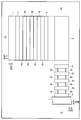
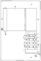
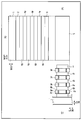
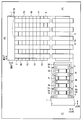
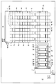
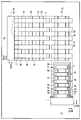
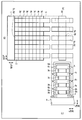
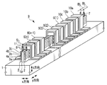
- the perspective view which shows the whole structure of a 1st Example The perspective view which shows the principal part of the structure of a 1st Example.
- the perspective view which shows the 1st modification of a 1st Example The perspective view which shows the 2nd modification of a 1st Example.
- the perspective view which shows the 1st example of a NAND cell unit structure Sectional drawing which follows the VI-VI line of FIG. Sectional drawing which follows the VII-VII line of FIG.
- the perspective view which shows the 2nd example of NAND cell unit structure Sectional drawing which follows the IX-IX line of FIG. Sectional drawing which follows the XX line of FIG.
- the perspective view which shows the 3rd example of a NAND cell unit structure The perspective view which shows the 3rd example of a NAND cell unit structure.
- FIG. 1st Example Sectional drawing which follows the XII-XII line
- the figure which shows the 1st example of the manufacturing method of a 1st Example The figure which shows the 1st example of the manufacturing method of a 1st Example.
- the figure which shows the 1st example of the manufacturing method of a 1st Example The figure which shows the 1st example of the manufacturing method of a 1st Example.
- the figure which shows the 1st example of the manufacturing method of a 1st Example The figure which shows the 1st example of the manufacturing method of a 1st Example.
- the figure which shows the 2nd example of the manufacturing method of a 1st Example The figure which shows the 2nd example of the manufacturing method of a 1st Example.
- the figure which shows the 2nd example of the manufacturing method of a 1st Example The figure which shows the 2nd example of the manufacturing method of a 1st Example.
- the figure which shows the 2nd example of the manufacturing method of a 1st Example The figure which shows the 2nd example of the manufacturing method of a 1st Example.
- the figure which shows the 2nd example of the manufacturing method of a 1st Example The figure which shows the 2nd example of the manufacturing method of a 1st Example.
- the figure which shows the 2nd example of the manufacturing method of a 1st Example The figure which shows the 2nd example of the manufacturing method of a 1st Example.
- the figure which shows the 2nd example of the manufacturing method of a 1st Example The figure which shows the 2nd example of the manufacturing method of a 1st Example.
- the figure which shows the 2nd example of the manufacturing method of a 1st Example The figure which shows the 2nd example of the manufacturing method of a 1st Example.
- the figure which shows the 2nd example of the manufacturing method of a 1st Example The figure which shows the 2nd example of the manufacturing method of a 1st Example.
- the figure which shows the 2nd example of the manufacturing method of a 1st Example The figure which shows the 2nd example of the manufacturing method of a 1st Example.
- the figure which shows the 2nd example of the manufacturing method of a 1st Example The perspective view which shows the whole structure of a 2nd Example.
- the perspective view which shows the modification of a 2nd Example The figure which shows the manufacturing method of a 2nd Example.
- the figure which shows the manufacturing method of a 2nd Example The figure which shows the manufacturing method of a 2nd Example.
- the figure which shows the manufacturing method of a 2nd Example. The figure which shows the manufacturing method of a 2nd Example.
- the figure which shows the manufacturing method of a 2nd Example The perspective view which shows the whole structure of a 3rd Example.
- the perspective view which shows the 1st modification of a 3rd Example The perspective view which shows the 2nd example of the manufacturing method of a 3rd Example.
- the perspective view which shows the 2nd modification of a 3rd Example The figure which shows the manufacturing method of a 3rd Example.
- the figure which shows the manufacturing method of a 3rd Example. The figure which shows the manufacturing method of a 3rd Example.
- the figure which shows the manufacturing method of a 3rd Example. The figure which shows the manufacturing method of a 3rd Example.
- the figure which shows the manufacturing method of a 3rd Example. The figure which shows the manufacturing method of a 3rd Example.
- the figure which shows the manufacturing method of a 3rd Example The figure which shows the manufacturing method of a 3rd Example.
- the figure which shows the manufacturing method of a 3rd Example. The figure which shows the manufacturing method of a 3rd Example.
- the figure which shows the manufacturing method of a 3rd Example. The figure which shows the manufacturing method of a 3rd Example.
- the figure which shows the manufacturing method of a 3rd Example. The figure which shows the manufacturing method of a 3rd Example.
- the basic idea of the present invention is that the first to nth semiconductor layers (stacked in a first direction perpendicular to the surface of the semiconductor substrate are insulated from each other and extend in a second direction parallel to the surface of the semiconductor substrate).
- n is a natural number of 2 or more
- electrodes extending in the first direction along the side surfaces of the first to nth semiconductor layers in the third direction intersecting the first and second directions, and the first to second
- the first to nth charge storage layers are made independent of each other, and writing / erasing is performed.
- the aim is to improve characteristics and cycling resistance.
- the first to nth charge storage layers are independent of each other, that the first to nth charge storage layers are physically separated, specifically, the first to nth charge storage layers. It means that there are elements different from the elements constituting them between the charge storage layers.
- the first to nth charge storage layers are generally physically coupled to each other.
- this causes a problem that the electrons injected into the charge storage layer of a certain memory cell diffuse to the charge storage layers of other memory cells adjacent to the memory cell and data is lost.
- the first to nth charge storage layers are made independent from each other to improve the write / erase characteristics and the cycling resistance.
- the independence of the charge storage layer in the present invention cannot be realized by simply diverting the independence of the charge storage layer employed in the conventional two-dimensional NAND flash memory. This is because it is impossible to directly change a two-dimensional memory cell into a three-dimensional memory cell.
- the independence of the charge storage layer in the present invention is based on the elements of the first to nth semiconductor layers and the first to nth charge storage layers from the viewpoint of memory cell characteristics and the prevention of complexity of the number of manufacturing steps. This is realized by physically separating the first to nth charge storage layers from each other by one of oxides of constituent materials.
- the present invention proposes a structure in which the charge storage layer is independent for each memory cell, for example, as a SONOS type memory cell using silicon-rich SiN as a charge storage layer, as an electrically floating floating gate
- the present invention can also be applied to a floating gate type memory cell using the above-described conductor as a charge storage layer.
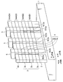
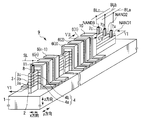
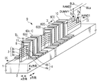
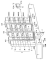
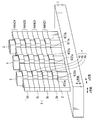
- FIG. 1 shows a nonvolatile semiconductor memory device as a first embodiment.
- FIG. 2 shows a structure in which the second gate insulating layer 6 (1) c and the control gate electrode 6 (1) d are removed from the structure of FIG.
- the semiconductor substrate 1 is, for example, a silicon substrate. On the semiconductor substrate 1, a fin-type stacked structure extending in the y direction parallel to the surface of the semiconductor substrate 1 is disposed.
- This fin-type stacked structure has a first insulating layer 2, a first semiconductor layer 3a, a second insulating layer 4a, and a second semiconductor layer 3b that are stacked in the z direction perpendicular to the surface of the semiconductor substrate 1. , A third insulating layer 4b, a third semiconductor layer 3c, a fourth insulating layer 4c, a fourth semiconductor layer 3d, and a fifth insulating layer 5.
- the first to fifth insulating layers 2, 4a to 4c, 5 may be anything as long as they are insulators.
- silicon oxide can be used.
- the first to fourth semiconductor layers 3a to 3d are made of, for example, silicon.
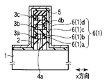
- the first gate insulating layer 6 (1) a On the x direction side of the first to fourth semiconductor layers 3 (3a, 3b, 3c, 3d), the first gate insulating layer 6 (1) a, the charge storage layer 6 (1) b, A stacked structure 6 (1) is disposed in which the second gate insulating layer 6 (1) c and the control gate electrode 6 (1) d are stacked in this order.
- the first gate insulating layer 6 (1) a is a tunnel insulating layer through which a tunnel current flows, and is made of, for example, silicon oxide.
- the charge storage layer 6 (1) b is a layer that stores charges, and the amount of charges is controlled by a tunnel current.
- the charge storage layer 6 (1) b is made of an insulator or a conductor.
- the memory cell is a SONOS type, and when the charge storage layer 6 (1) a is a conductor (for example, conductive polysilicon).
- the memory cell becomes a floating gate type.
- the charge storage layer 6 (1) b is independent for each memory cell.
- the four charge storage layers 6 (1) b,... Arranged side by side in the z direction are elements between the first to fourth semiconductor layers 3 (3a, 3b, 3c, 3d), in this example,
- the second to fourth insulating layers 4 (4a, 4b, 4c) are physically separated from each other.
- the second gate insulating layer 6 (1) c prevents a leakage current between the charge storage layer 6 (1) b and the control gate electrode 6 (1) d.
- the second gate insulating layer 6 (1) c is formed of, for example, a stacked structure or a high dielectric constant material in order to increase the coupling ratio of the memory cell and improve the write / erase characteristics. .
- the second gate insulating layer 6 (1) c is generally called a block insulating layer, and when the memory cell is a floating gate type, the second gate insulating layer 6 (1). c is generally referred to as an interelectrode insulating layer.
- the control gate electrode 6 (1) d functions as a word line, extends in the x-direction on the z-direction side of the fifth insulating layer 5, and the first to fourth semiconductor layers 3 (3a, 3b, 3c, 3d) Extends in the z direction on the x direction side.
- control gate electrode 6 (1) d covers the four charge storage layers 6 (1) b,... And straddles the fin-type stacked structure in the x direction.
- the laminated structures 6 (2) and 6 (3) have the same structure as the laminated structure 6 (1).
- each of the first to fourth semiconductor layers 3 (3a, 3b, 3c, 3d) has a plurality of memory cell columns connected in series in the y direction, that is, NAND columns. It is formed.
- the NAND string formed in the first semiconductor layer 3a is NAND1
- the NAND string formed in the second semiconductor layer 3b is NAND2
- the NAND string formed in the third semiconductor layer 3c is NAND3.
- the NAND string formed in the fourth semiconductor layer 3d is NAND4.
- the charge storage layer 6 (1) b is independent for each memory cell. That is, the plurality of charge storage layers 6 (1) b,... Are physically separated from each other by the second to fourth insulating layers 4 (4a, 4b, 4c). Therefore, the reliability of the three-dimensional stacked semiconductor memory can be improved.
- the first gate insulating layer 6 (1) a is made of SiO 2
- the charge storage layer 6 (1) b is made of Si 3 N 4
- the second gate insulating layer 6 (1) c is made of Al 2 O 3 and the control gate electrode 6 (1) d can be NiSi.
- the first gate insulating layer 6 (1) a may have silicon oxynitride, a stacked structure of silicon oxide and silicon nitride, or the like.
- the first gate insulating layer 6 (1) a may contain silicon nanoparticles, metal ions, or the like.
- the charge storage layer 6 (1) b is composed of Si x N y , silicon oxynitride (SiON), aluminum oxide (Al 2 O 3 ), and aluminum oxynitride (AlON) in which the composition ratio x and y of silicon and nitrogen are arbitrary.
- Hafnia HfO 2
- hafnium aluminate HfAlO 3
- hafnia nitride HfON
- nitrided hafnium aluminate HfAlON
- hafnium silicate HfSiO
- nitrided hafnium silicate HfSiON
- lanthanum oxide La 2 O 3
- at least one of lanthanum aluminate LaAlO 3
- the charge storage layer 6 (1) b may be made of a conductor such as polysilicon or metal doped with impurities.
- the second gate insulating layer 6 (1) c includes silicon oxide (SiO 2 ), silicon oxynitride (SiON), aluminum oxide (Al 2 O 3 ), aluminum oxynitride (AlON), hafnia (HfO 2 ), and hafnium. ⁇ Aluminate (HfAlO 3 ), Hafnia nitride (HfON), Hafnium nitride aluminate (HfAlON), Hafnium silicate (HfSiO), Hafnium nitride silicate (HfSiON), Lanthanum oxide (La 2 O 3 ), Lanthanum aluminum Nate (LaAlO 3 ) and lanthanum aluminum silicate (LaAlSiO) may be used.
- the control gate electrode 6 (1) d is a metal compound such as tantalum nitride (TaN), tantalum carbide (TaC), or titanium nitride (TiN), or V, Cr, Mn, Y, Mo, Ru, Rh, Hf, Ta, W, Ir, Co, Ti, Er, Pt, Pd, Zr, Gd, Dy, Ho and their silicides can be used.
- TaN tantalum nitride
- TaC tantalum carbide
- TiN titanium nitride
- V Cr, Mn, Y, Mo, Ru, Rh, Hf, Ta, W, Ir, Co, Ti, Er, Pt, Pd, Zr, Gd, Dy, Ho and their silicides
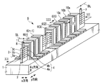
- FIG. 3 shows a first modification of the first embodiment.
- a feature of the first modification is that a dummy cell as a non-memory cell is formed on the uppermost layer of the first to fourth semiconductor layers 3 (3a, 3b, 3c, 3d), that is, the fourth semiconductor layer 3d.
- the dummy layer is to be DUMMY.
- the fourth semiconductor layer 3d as the uppermost layer is easily damaged because it is used as an etching mask in one step of the first and second manufacturing methods described later. For this reason, the NAND string formed in the fourth semiconductor layer 3d is not used as a memory cell but a dummy cell as a non-memory cell.
- the width of the fourth semiconductor layer 3d in the z direction is the width of the first to third semiconductor layers 3a, 3b, 3c in the z direction. It is preferable to make it wider.
- FIG. 4 shows a second modification of the first embodiment.
- the feature of the second modification is that the four charge storage layers 6 (1) b,... Arranged side by side in the z direction are physically separated from each other by a cavity (for example, an air gap). That is, in the second modification, the element between the first to fourth semiconductor layers 3 (3a, 3b, 3c, 3d) is a cavity.
- the parasitic capacitance generated between the plurality of charge storage layers 6 (1) b increases, causing malfunction due to mutual interference.
- all of the first to fifth insulating layers 2, 4a to 4c, 5 in the first embodiment are changed to cavities, but only some of them are changed to cavities. May be.
- the cavity is preferably a complete cavity, but an insulator may partially remain.
- the cavity can be changed to a porous insulator.
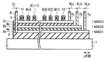
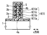
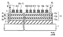
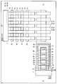
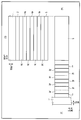
- FIG. 5 shows a first example of a NAND cell unit structure.
- 6 is a cross-sectional view taken along line VI-VI in FIG. 5
- FIG. 7 is a cross-sectional view taken along line VII-VII in FIG.
- This example shows a NAND cell unit structure as an application example of the first embodiment (FIGS. 1 and 2). Accordingly, the same elements as those in the first embodiment are denoted by the same reference numerals. This example is different from the first embodiment in that the number of NAND strings NAND1, NAND2, NAND3 is three.
- the fin-type stacked structure 9 includes a first insulating layer 2, a first semiconductor layer 3a, a second insulating layer 4a, a second semiconductor layer 3b, and a third insulating layer, which are stacked on the semiconductor substrate 1 in the z direction.
- the layer 4b, the third semiconductor layer 3c, and the fifth insulating layer 5 are included.
- the one end of the fin type laminated structure 9 in the y direction has a staircase structure. At one end in the y direction of the fin-type stacked structure 9, the side surfaces in the z direction of the first to third semiconductor layers 3 (3a, 3b, 3c) are exposed. The contact plugs 7a, 7b, 7c are in contact with the side surfaces in the z direction of the first to third semiconductor layers 3 (3a, 3b, 3c), respectively.
- the contact plugs 7a, 7b, and 7c connect the bit lines BLa, BLb, and BLc to the NAND series NAND1, NAND2, and NAND3, respectively.
- the contact plug 8 penetrates the first to third semiconductor layers 3 (3a, 3b, 3c) and contacts them.
- the contact plug 8 connects the source line SL to the NAND series NAND1, NAND2, NAND3.
- the stacked structures 6 (1),... 6 (n-1), 6 (n) each constitute a memory cell.
- the stacked structure 6 (1) includes a first gate insulating layer 6 (1) a, a charge storage layer 6 (1) b, a second gate insulating layer 6 (1) c, and a control gate electrode 6 (1) d. Composed.
- the other stacked structures 6 (2),... 6 (n-1), 6 (n) also have the same structure as the stacked structure 6 (1).
- the laminated structures 10 and 11 also have the same structure as the laminated structure 6 (1).
- the stacked structures 10 and 11 each constitute a selection transistor.
- the stacked structure 10 constitutes a drain side select transistor, and the stacked structure 11 constitutes a source side select transistor.
- the NAND cell unit can be configured using the NAND string of the first embodiment, a highly reliable three-dimensional NAND flash memory can be realized.
- FIG. 8 shows a second example of the NAND cell unit structure.
- 9 is a cross-sectional view taken along line IX-IX in FIG. 8
- FIG. 10 is a cross-sectional view taken along line XX in FIG.
- This example shows a NAND cell unit structure as an application example of the first modification (FIG. 3). Accordingly, the same elements as those in the first modification are denoted by the same reference numerals. This example is different from the first modification in that the number of NAND strings NAND1, NAND2, NAND3 is three.
- the fin-type stacked structure 9 includes a first insulating layer 2, a first semiconductor layer 3a, a second insulating layer 4a, a second semiconductor layer 3b, and a third insulating layer, which are stacked on the semiconductor substrate 1 in the z direction.
- the layer 4b, the third semiconductor layer 3c, and the fifth insulating layer 5 are included.
- the one end of the fin type laminated structure 9 in the y direction has a staircase structure. At one end in the y direction of the fin-type stacked structure 9, the side surfaces in the z direction of the first to third semiconductor layers 3 (3a, 3b, 3c) are exposed. The contact plugs 7a and 7b are in contact with the side surfaces in the z direction of the first and second semiconductor layers 3a and 3b, respectively.
- the contact plugs 7a and 7b connect the bit lines BLa and BLb to the NAND strings NAND1 and NAND2, respectively.
- the third semiconductor layer 3c is a dummy layer DUMMY, no contact plug is connected thereto.
- the contact plug 8 penetrates the first to third semiconductor layers 3 (3a, 3b, 3c) and contacts them.
- the contact plug 8 connects the source line SL to the NAND series NAND1, NAND2, NAND3.
- the stacked structures 6 (1),... 6 (n-1), 6 (n) each constitute a memory cell. However, the dummy cell formed in the third semiconductor layer 3c as the dummy layer DUMMY is excluded.
- the stacked structure 6 (1) includes a first gate insulating layer 6 (1) a, a charge storage layer 6 (1) b, a second gate insulating layer 6 (1) c, and a control gate electrode 6 (1) d. Composed.
- the other stacked structures 6 (2),... 6 (n-1), 6 (n) also have the same structure as the stacked structure 6 (1).
- the laminated structures 10 and 11 also have the same structure as the laminated structure 6 (1).
- the stacked structures 10 and 11 each constitute a selection transistor. However, the dummy transistor formed in the third semiconductor layer 3c as the dummy layer DUMMY is excluded.
- the stacked structure 10 constitutes a drain side select transistor, and the stacked structure 11 constitutes a source side select transistor.
- the NAND cell unit can be configured by using the NAND string of the first modification, a highly reliable three-dimensional NAND flash memory can be realized.
- FIG. 11 shows a third example of the NAND cell unit structure.
- 12 is a cross-sectional view taken along line XII-XII in FIG. 11
- FIG. 13 is a cross-sectional view taken along line XIII-XIII in FIG.
- This example is a modification of the first example of the NAND cell unit structure. Accordingly, the same elements as those in FIGS. 5 to 7 are denoted by the same reference numerals.
- the laminated structure 10 includes three laminated structures 10a, 10b, and 10c.
- the stacked structures 10a, 10b, and 10c are the same as the stacked structure 10 shown in FIGS.
- an impurity region 13a is provided so that the drain side select transistor is always on (normally on).
- an impurity region 13b is provided in the portion covered with the stacked structure 10b in the second semiconductor layer 3b so that the drain side select transistor is normally on.
- an impurity region 13c is provided in a portion of the third semiconductor layer 3c covered with the stacked structure 10c so that the drain side select transistor is normally on.
- the contact plug 7 can be shared also at one end in the y direction of the fin-type laminated structure 9. That is, the contact plug 7 penetrates through and contacts the first to third semiconductor layers 3 (3a, 3b, 3c).
- the contact plug 7 connects the bit line BL to the NAND series NAND1, NAND2, NAND3.
- NAND cell unit structure In the first embodiment (FIGS. 1 and 2), laminated structures 10a, 10b, and 10c as shown in FIGS. 11 to 13 may be employed.
- laminated structures 10a, 10b, and 10c as shown in FIGS. 11 to 13 may be employed.
- the cell unit structure as shown in FIGS. 5 to 7 the cell unit structure as shown in FIGS. 8 to 10
- the stack as shown in FIGS. Structures 10a, 10b, and 10c may be employed.
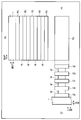
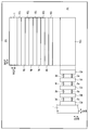
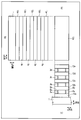
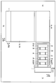
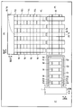
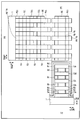
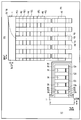
- FIGS. 14A to 14L A method of manufacturing the structure according to the first embodiment (FIGS. 1 and 2) and the first modification (FIG. 3) will be described below with reference to FIGS. 14A to 14L.
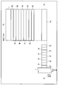
- (a) is a plan view
- (b) is a side view when viewed from the x direction
- (c) is a side view when viewed from the y direction.
- the first insulating layer 2, the first semiconductor layer 3a, the second insulating layer 4a, and the second semiconductor layer 3b are arranged in the z direction perpendicular to the surface of the semiconductor substrate 1.
- the third insulating layer 4b, the third semiconductor layer 3c, the fourth insulating layer 4c, the fourth semiconductor layer 3d, and the fifth insulating layer 5 are sequentially formed.
- the semiconductor substrate 1 is a p-type silicon substrate having a plane orientation (100) and a specific resistance of 10 to 20 ⁇ cm
- the first to fifth insulating layers 2, 4a to 4c, and 5 are made of silicon oxide
- the first to fourth semiconductor layers 3a to 3d are made of silicon.
- the first to fifth insulating layers 2, 4a to 4c, 5 and the first to fourth semiconductor layers 3a to 3d are processed by PEP (photo-engraving process) and anisotropic dry etching to obtain a semiconductor substrate.
- PEP photo-engraving process
- anisotropic dry etching to obtain a semiconductor substrate.
- a fin-type laminated structure extending in the y direction parallel to the surface of 1 is formed.
- the side surfaces of the first to fourth semiconductor layers 3a to 3d in the x direction are selectively etched in the x direction by isotropic dry etching.
- the side surfaces in the x direction of the first to fourth semiconductor layers 3a to 3d recede, and the first to fourth recesses 21a to 21d extending in the y direction are formed.
- a first gate insulating layer (for example, silicon oxide) 6a is formed on each side.
- a charge storage layer 6b covering the fin-type stacked structure is formed.
- a material such as silicon nitride or conductive polysilicon can be used for the charge storage layer 6b.
- the charge storage layer 6b is selectively etched by anisotropic dry etching. As a result, the charge storage layer 6b remains only in the first to fourth recesses 21a to 21d on the side surface in the x direction of the first to fourth semiconductor layers 3a to 3d.
- the fifth insulating layer 5 is exposed. Therefore, if the charge storage layer 6b is further etched using the fifth insulating layer 5 as a mask, the first through First to fourth charge storage layers 6b are formed in the fourth recesses 21a to 21d, respectively.
- the width of the fifth insulating layer 5 in the z direction is the first to fourth insulating layers 2 and 4a. It may be larger than the width in the z direction of 4c.
- the fifth insulating layer 5 places importance on the function as a mask and is different from the first to fourth insulating layers 2 and 4a to 4c in a different method or a different material (for example, a laminated structure including a plurality of different insulating layers). ).
- the first to fourth charge storage layers 6b are separated in the z direction.
- a second gate insulating layer 6c and a control gate electrode 6d that cover the fin-type stacked structure (including the first to fourth charge storage layers 6b) are formed.
- a material such as aluminum oxide can be used for the second gate insulating layer 6c, and a material such as nickel silicide can be used for the control gate electrode 6d.
- the second gate insulating layer 6c and the control gate electrode 6d are processed by PEP and anisotropic dry etching to form a plurality of control gate electrodes (word lines) 6d,. .
- the plurality of control gate electrodes (word lines) 6d,... Extend in the x direction on the z direction side of the fifth insulating layer 5, and in the z direction on the x direction side of the first to fourth charge storage layers 6b. Extend.
- the fifth insulating layer 5 is selectively etched by anisotropic dry etching.
- the plurality of control gate electrodes 6d,... Function as a mask for anisotropic dry etching. Therefore, the fifth insulating layer 5 is selectively removed in a portion not covered with the plurality of control gate electrodes 6d,... And the side surfaces in the z direction of the fourth semiconductor layer 3d and the fourth charge storage layer 6b. Are exposed.
- the fourth charge storage layer 6b is selectively etched by anisotropic dry etching.
- the plurality of control gate electrodes 6d,... And the fourth semiconductor layer 3d each function as a mask for anisotropic dry etching.
- the fourth semiconductor layer 3d is separated in the y direction on the x direction side.
- a plurality of fourth charge storage layers 6b,... Are formed.
- the fourth insulating layer 4c is selectively etched by anisotropic dry etching.
- the plurality of control gate electrodes 6d,... And the fourth semiconductor layer 3d each function as a mask for anisotropic dry etching.
- the fourth insulating layer 4c is selectively removed in a portion not covered with the plurality of control gate electrodes 6d,... And the fourth semiconductor layer 3d, and the side surface in the z direction of the third charge storage layer 6b. Are exposed.
- the third charge storage layer 6b is selectively etched by anisotropic dry etching.
- the plurality of control gate electrodes 6d,... And the fourth semiconductor layer 3d each function as a mask for anisotropic dry etching.
- the portion of the third charge storage layer 6b not covered by the plurality of control gate electrodes 6d,... is selectively removed, so that the third semiconductor layer 3c is separated in the y direction on the x direction side.
- a plurality of third charge storage layers 6b,... Are formed.
- a plurality of second charge storage layers 6b,... Separated in the y direction are formed on the x direction side of the second semiconductor layer 3b, and the y direction side of the first semiconductor layer 3a is formed on the y direction side.
- a plurality of first charge storage layers 6b,... Separated in the direction are formed.
- the fourth semiconductor layer 3d as the uppermost layer functions as an etching mask during the etching for realizing the independence of the charge storage layer. .
- the fourth semiconductor layer 3d is a dummy layer, and the width of the fourth semiconductor layer 3d in the z direction is larger than the width of the first to third semiconductor layers 3a to 3c in the z direction. preferable.
- FIG. 4 is a plan view
- FIGS. 15A to 15N are views of the structure according to the second modification.
- (a) is a plan view
- (b) is a side view when viewed from the x direction
- (c) is a side view when viewed from the y direction.
- the first temporary layer 12a in the z direction perpendicular to the surface of the semiconductor substrate 1, the first temporary layer 12a, the first semiconductor layer 3a, the second temporary layer 12b, and the second semiconductor layer 3b.
- the third temporary layer 12c, the third semiconductor layer 3c, the fourth temporary layer 12d, the fourth semiconductor layer 3d, and the fifth temporary layer 12e are sequentially formed.
- the semiconductor substrate 1 is, for example, a p-type silicon substrate having a plane orientation (100) and a specific resistance of 10 to 20 ⁇ cm, and the first to fifth temporary layers 12a to 12e are made of silicon germanium.
- the semiconductor layers 3a to 3d are made of silicon.
- single crystal silicon can be obtained by alternately stacking both layers by epitaxial growth. For this reason, variation in characteristics between the first to fourth semiconductor layers (silicon channels) 3a to 3d is reduced, and the channel mobility of the silicon channel can be improved.
- first to fifth temporary layers 12a to 12e and the first to fourth semiconductor layers 3a to 3d are processed by PEP and anisotropic dry etching so as to be parallel to the surface of the semiconductor substrate 1 in the y direction.
- An extending fin-type stacked structure is formed.
- the side surfaces of the first to fourth semiconductor layers 3a to 3d in the x direction are selectively etched in the x direction by isotropic dry etching.
- the side surfaces in the x direction of the first to fourth semiconductor layers 3a to 3d recede, and the first to fourth recesses 21a to 21d extending in the y direction are formed.
- a first gate insulating layer (for example, silicon oxide) 6a is formed on each side.
- a charge storage layer 6b covering the fin-type stacked structure is formed.
- a material such as silicon nitride or conductive polysilicon can be used for the charge storage layer 6b.
- the charge storage layer 6b is selectively etched by anisotropic dry etching. As a result, the charge storage layer 6b remains only in the first to fourth recesses 21a to 21d on the side surface in the x direction of the first to fourth semiconductor layers 3a to 3d.
- the fifth temporary layer 12e is exposed when the uppermost charge storage layer 6b is removed, if the charge storage layer 6b is further etched using the fifth temporary layer 12e as a mask, the first through First to fourth charge storage layers 6b are formed in the fourth recesses 21a to 21d, respectively.
- the width of the fifth temporary layer 12e in the z direction is the first to fourth temporary layers 12a to 12d. It may be larger than the width in the z direction.
- the fifth temporary layer 12e may be configured by a different method or a different material from the first to fourth temporary layers 12a to 12d, focusing on the function as a mask.
- the first to fourth charge storage layers 6b are separated in the z direction.
- a second gate insulating layer 6c and a control gate electrode 6d that cover the fin-type stacked structure (including the first to fourth charge storage layers 6b) are formed.
- a material such as aluminum oxide can be used for the second gate insulating layer 6c, and a material such as nickel silicide can be used for the control gate electrode 6d.
- the second gate insulating layer 6c and the control gate electrode 6d are processed by PEP and anisotropic dry etching to form a plurality of control gate electrodes (word lines) 6d,. .
- the plurality of control gate electrodes (word lines) 6d,... Extend in the x direction on the z direction side of the fifth temporary layer 12e, and extend in the z direction on the x direction side of the first to fourth charge storage layers 6b. Extend.
- the fifth temporary layer 12e is selectively etched by anisotropic dry etching.
- the plurality of control gate electrodes 6d,... Function as a mask for anisotropic dry etching. Therefore, the fifth temporary layer 12e is selectively removed in a portion not covered with the plurality of control gate electrodes 6d,..., And the side surfaces in the z direction of the fourth semiconductor layer 3d and the fourth charge storage layer 6b. Are exposed.
- the fourth charge storage layer 6b is selectively etched by anisotropic dry etching.
- the plurality of control gate electrodes 6d,... And the fourth semiconductor layer 3d each function as a mask for anisotropic dry etching.
- the fourth semiconductor layer 3d is separated in the y direction on the x direction side.
- a plurality of fourth charge storage layers 6b,... Are formed.
- the fourth temporary layer 12d is selectively etched by anisotropic dry etching.
- the plurality of control gate electrodes 6d,... And the fourth semiconductor layer 3d each function as a mask for anisotropic dry etching.
- the fourth temporary layer 12d is selectively removed in the portion not covered with the plurality of control gate electrodes 6d,... And the fourth semiconductor layer 3d, and the side surface of the third charge storage layer 6b in the z direction is removed. Are exposed.
- the third charge storage layer 6b is selectively etched by anisotropic dry etching.
- the plurality of control gate electrodes 6d,... And the fourth semiconductor layer 3d each function as a mask for anisotropic dry etching.
- the portion of the third charge storage layer 6b not covered by the plurality of control gate electrodes 6d,... is selectively removed, so that the third semiconductor layer 3c is separated in the y direction on the x direction side.
- a plurality of third charge storage layers 6b,... Are formed.
- a plurality of second charge storage layers 6b,... Separated in the y direction are formed on the x direction side of the second semiconductor layer 3b, and the y direction side of the first semiconductor layer 3a is formed on the y direction side.
- a plurality of first charge storage layers 6b,... Separated in the direction are formed.
- the first to fifth temporary layers 12a to 12e are selectively removed by isotropic dry etching, and the upper and lower sides of the first to fourth semiconductor layers 3a to 3d ( Cavities 22,... are respectively formed on the z direction side).
- the first to fifth temporary layers 12a to 12e are spaces between the plurality of control gate electrodes 6d, and further, the first to fourth semiconductor layers 3a to 3d (first to fourth). Are exposed in the space between the charge storage layers 6b,(7) And can be easily removed by isotropic dry etching.
- the cavities 22 may be left as they are, but as shown in FIG. 15N, the cavities 22 may be filled with an insulating layer (for example, silicon oxide) 13. At this time, the insulating layer 13 may be a porous insulating layer.
- an insulating layer for example, silicon oxide
- the fourth semiconductor layer 3d as the uppermost layer functions as an etching mask during etching for realizing the independence of the charge storage layer. To do.
- the fourth semiconductor layer 3d is a dummy layer, and the width of the fourth semiconductor layer 3d in the z direction is larger than the width of the first to third semiconductor layers 3a to 3c in the z direction. preferable.
- high reliability of the three-dimensional stacked semiconductor memory can be realized by forming the structure in which the charge storage layer is independent for each memory cell without significantly increasing the number of processes. .
- FIG. 16 shows a nonvolatile semiconductor memory device as a second embodiment.
- FIG. 17 shows a structure in which the second gate insulating layer 6 (1) c and the control gate electrode 6 (1) d are removed from the structure of FIG.
- the semiconductor substrate 1 is, for example, a silicon substrate. On the semiconductor substrate 1, a fin-type stacked structure extending in the y direction parallel to the surface of the semiconductor substrate 1 is disposed.
- This fin-type stacked structure has a first insulating layer 2, a first semiconductor layer 3a, a second insulating layer 4a, and a second semiconductor layer 3b that are stacked in the z direction perpendicular to the surface of the semiconductor substrate 1. , A third insulating layer 4b, a third semiconductor layer 3c, a fourth insulating layer 4c, a fourth semiconductor layer 3d, and a fifth insulating layer 5.
- the first to fifth insulating layers 2, 4a to 4c, 5 may be anything as long as they are insulators.
- silicon oxide can be used.
- the first to fourth semiconductor layers 3a to 3d are made of, for example, silicon.
- the first gate insulating layer 6 (1) a On the x direction side of the first to fourth semiconductor layers 3 (3a, 3b, 3c, 3d), the first gate insulating layer 6 (1) a, the charge storage layer 6 (1) b, A stacked structure 6 (1) is disposed in which the second gate insulating layer 6 (1) c and the control gate electrode 6 (1) d are stacked in this order.
- the first gate insulating layer 6 (1) a is a tunnel insulating layer through which a tunnel current flows, and is made of, for example, silicon oxide.
- the charge storage layer 6 (1) b is a layer that stores charges, and the amount of charges is controlled by a tunnel current.
- the charge storage layer 6 (1) b is made of an insulator or a conductor.
- the memory cell is a SONOS type, and when the charge storage layer 6 (1) a is a conductor (for example, conductive polysilicon).
- the memory cell becomes a floating gate type.
- the charge storage layer 6 (1) b is independent for each memory cell.
- the four charge storage layers 6 (1) b,... Arranged side by side in the z-direction are oxides of materials constituting the four charge storage layers 6 (1) b,.
- the layer 6 (1) b is silicon nitride, it is physically separated from each other by silicon oxynitride 14).
- the second gate insulating layer 6 (1) c prevents a leakage current between the charge storage layer 6 (1) b and the control gate electrode 6 (1) d.
- the second gate insulating layer 6 (1) c is formed of, for example, a stacked structure or a high dielectric constant material in order to increase the coupling ratio of the memory cell and improve the write / erase characteristics. .
- the second gate insulating layer 6 (1) c is generally called a block insulating layer, and when the memory cell is a floating gate type, the second gate insulating layer 6 (1). c is generally referred to as an interelectrode insulating layer.
- the control gate electrode 6 (1) d functions as a word line, extends in the x-direction on the z-direction side of the fifth insulating layer 5, and the first to fourth semiconductor layers 3 (3a, 3b, 3c, 3d) Extends in the z direction on the x direction side.
- control gate electrode 6 (1) d covers the four charge storage layers 6 (1) b,... And straddles the fin-type stacked structure in the x direction.
- the laminated structures 6 (2) and 6 (3) have the same structure as the laminated structure 6 (1).
- each of the first to fourth semiconductor layers 3 (3a, 3b, 3c, 3d) has a plurality of memory cell columns connected in series in the y direction, that is, NAND columns. It is formed.
- the NAND string formed in the first semiconductor layer 3a is NAND1
- the NAND string formed in the second semiconductor layer 3b is NAND2
- the NAND string formed in the third semiconductor layer 3c is NAND3.
- the NAND string formed in the fourth semiconductor layer 3d is NAND4.
- the charge storage layer 6 (1) b is independent for each memory cell. That is, the plurality of charge storage layers 6 (1) b,... Are physically separated from each other by the oxide 14 of the material constituting the four charge storage layers 6 (1) b,. Therefore, the reliability of the three-dimensional stacked semiconductor memory can be improved.
- first gate insulating layer 6 (1) a For material examples of the first gate insulating layer 6 (1) a, the charge storage layer 6 (1) b, the second gate insulating layer 6 (1) c, and the control gate electrode 6 (1) d, Since it is the same as the embodiment, its description is omitted here.
- FIG. 18 shows a modification of the second embodiment.
- the feature of this modification is that the four charge storage layers 6 (1) b,... Arranged side by side in the z direction are physically separated from each other by a cavity (for example, an air gap). That is, in this modification, the element between the first to fourth semiconductor layers 3 (3a, 3b, 3c, 3d) is a cavity.
- the parasitic capacitance generated between the plurality of charge storage layers 6 (1) b increases, causing malfunction due to mutual interference.
- all of the first to fifth insulating layers 2, 4a to 4c, 5 in the second embodiment are changed to cavities, but only some of them are changed to cavities. May be.
- the cavity is preferably a complete cavity, but an insulator may partially remain.
- the cavity can be changed to a porous insulator.
- Example of NAND cell unit structure The NAND cell unit structure to which the second embodiment (FIGS. 16 and 17) is applied can be the NAND cell unit structure of FIGS. 5 to 7 or the NAND cell unit structure of FIGS. . However, in these NAND cell unit structures, the NAND cell unit portion needs to be changed to the structure shown in FIGS.
- the cell unit structure as shown in FIGS. 5 to 7 or the cell unit structure as shown in FIGS. 11 to 13 can be adopted.
- the NAND cell unit portion needs to be changed to the structure shown in FIG.
- FIGS. 19A to 19E Manufacturing method A method of manufacturing a structure according to the second embodiment (FIGS. 16 and 17) and its modification (FIG. 18) will be described below with reference to FIGS. 19A to 19E.
- (a) is a plan view
- (b) is a side view when viewed from the x direction
- (c) is a side view when viewed from the y direction.
- the first temporary layer 12a in the z direction perpendicular to the surface of the semiconductor substrate 1, the first temporary layer 12a, the first semiconductor layer 3a, the second temporary layer 12b, and the second semiconductor layer 3b.
- the third temporary layer 12c, the third semiconductor layer 3c, the fourth temporary layer 12d, the fourth semiconductor layer 3d, and the fifth temporary layer 12e are sequentially formed.
- the semiconductor substrate 1 is, for example, a p-type silicon substrate having a plane orientation (100) and a specific resistance of 10 to 20 ⁇ cm, and the first to fifth temporary layers 12a to 12e are made of silicon germanium.
- the semiconductor layers 3a to 3d are made of silicon.
- single crystal silicon can be obtained by alternately stacking both layers by epitaxial growth. For this reason, variation in characteristics between the first to fourth semiconductor layers (silicon channels) 3a to 3d is reduced, and the channel mobility of the silicon channel can be improved.
- first to fifth temporary layers 12a to 12e and the first to fourth semiconductor layers 3a to 3d are processed by PEP and anisotropic dry etching so as to be parallel to the surface of the semiconductor substrate 1 in the y direction.
- An extending fin-type stacked structure is formed.
- the side surfaces in the x direction of the first to fourth semiconductor layers 3a to 3d, the side surfaces in the x direction of the first to fourth temporary layers 12a to 12d, and the fifth side by thermal oxidation are oxidized to form the first gate insulating layer (for example, silicon oxide) 6a on the side surfaces in the x direction of the first to fourth semiconductor layers 3a to 3d.
- the first gate insulating layer for example, silicon oxide
- a combined charge storage layer 6b, a second gate insulating layer 6c, and a control gate electrode 6d that cover the fin-type stacked structure (first gate insulating layer 6a) are sequentially formed.
- the coupled charge storage layer 6b for example, a material such as silicon nitride or conductive polysilicon can be used. Further, for example, a material such as aluminum oxide can be used for the second gate insulating layer 6c, and a material such as nickel silicide can be used for the control gate electrode 6d.
- the first gate insulating layer 6a, the combined charge storage layer 6b, the second gate insulating layer 6c, and the control gate electrode 6d are processed by PEP and anisotropic dry etching, and a plurality of control gate electrodes (word lines) are processed. ) 6d,.
- the plurality of control gate electrodes (word lines) 6d,... Extend in the x direction on the z direction side of the fifth temporary layer 12e, and extend in the z direction on the x direction side of the first to fourth charge storage layers 6b. Extend.
- the first gate insulating layer 6a, the combined charge storage layer 6b, and the second gate insulating layer 6c have the same shape as the control gate electrode 6d and are covered with the control gate electrode 6d.
- the first to fifth temporary layers 12a to 12e are selectively removed by isotropic dry etching, and the upper and lower sides of the first to fourth semiconductor layers 3a to 3d ( Cavities 22,... are respectively formed on the z direction side).
- the first to fifth temporary layers 12a to 12e are spaces between the plurality of control gate electrodes 6d, and further, the first to fourth semiconductor layers 3a to 3d (first to fourth). Are exposed in the space between the charge storage layers 6b,(7) And can be easily removed by isotropic dry etching.
- the combined charge storage layer 6b is selectively oxidized from the region where the first to fifth temporary layers 12a to 12e are removed.
- oxidation of the combined charge storage layer 6b proceeds from the region where the first to fifth temporary layers 12a to 12e are removed.
- the coupled charge storage layer 6b is not oxidized between the first to fourth semiconductor layers 3a to 3d and the control gate electrode 6d. Therefore, the combined charge storage layer 6b is changed into a plurality of charge storage layers 6b,... Physically separated from each other by the oxide 14 of the combined charge storage layer 6b.
- the side surfaces in the x direction of the plurality of charge storage layers 6b,... are covered with the first to fourth semiconductor layers 3a to 3d and the control gate electrode 6d, and the side surfaces in the y direction and the z direction are coupled.
- the charge storage layer 6 b is covered with the oxide 14.
- the cavities 22 may be left as they are, but as shown in FIG. 19E, the cavities 22 may be filled with an insulating layer (for example, silicon oxide) 15. At this time, the insulating layer 15 may be a porous insulating layer.
- an insulating layer for example, silicon oxide
- the high reliability of the three-dimensional stacked semiconductor memory can be realized by forming the structure in which the charge storage layer is independent for each memory cell without significantly increasing the number of processes. .
- FIG. 20 shows a nonvolatile semiconductor memory device as a third embodiment.
- FIG. 21 shows a structure in which the second gate insulating layer 6 (1) c and the control gate electrode 6 (1) d are removed from the structure of FIG.
- the semiconductor substrate 1 is, for example, a silicon substrate. On the semiconductor substrate 1, a fin-type stacked structure extending in the y direction parallel to the surface of the semiconductor substrate 1 is disposed.
- This fin-type stacked structure has a first insulating layer 2, a first semiconductor layer 3a, a second insulating layer 4a, and a second semiconductor layer 3b that are stacked in the z direction perpendicular to the surface of the semiconductor substrate 1. , A third insulating layer 4b, a third semiconductor layer 3c, a fourth insulating layer 4c, a fourth semiconductor layer 3d, and a fifth insulating layer 5.
- the first to fifth insulating layers 2, 4a to 4c, 5 may be anything as long as they are insulators.
- silicon oxide can be used.
- the first to fourth semiconductor layers 3a to 3d are made of, for example, silicon.
- the first gate insulating layer 6 (1) a On the x direction side of the first to fourth semiconductor layers 3 (3a, 3b, 3c, 3d), the first gate insulating layer 6 (1) a, the charge storage layer 6 (1) b, A stacked structure 6 (1) is disposed in which the second gate insulating layer 6 (1) c and the control gate electrode 6 (1) d are stacked in this order.
- the first gate insulating layer 6 (1) a is a tunnel insulating layer through which a tunnel current flows, and is made of, for example, silicon oxide.
- the charge storage layer 6 (1) b is a layer that stores charges, and the amount of charges is controlled by a tunnel current.
- the charge storage layer 6 (1) b is made of an insulator or a conductor.
- the memory cell is a SONOS type, and when the charge storage layer 6 (1) a is a conductor (for example, conductive polysilicon).
- the memory cell becomes a floating gate type.
- the charge storage layer 6 (1) b is independent for each memory cell.
- the four charge storage layers 6 (1) b,... Arranged side by side in the z direction are elements between the first to fourth semiconductor layers 3 (3a, 3b, 3c, 3d), in this example,
- the second to fourth insulating layers 4 (4a, 4b, 4c) are physically separated from each other.
- the second gate insulating layer 6 (1) c prevents a leakage current between the charge storage layer 6 (1) b and the control gate electrode 6 (1) d.
- the second gate insulating layer 6 (1) c is formed of, for example, a stacked structure or a high dielectric constant material in order to increase the coupling ratio of the memory cell and improve the write / erase characteristics. .
- the second gate insulating layer 6 (1) c is generally called a block insulating layer, and when the memory cell is a floating gate type, the second gate insulating layer 6 (1). c is generally referred to as an interelectrode insulating layer.
- the control gate electrode 6 (1) d functions as a word line, extends in the x-direction on the z-direction side of the fifth insulating layer 5, and the first to fourth semiconductor layers 3 (3a, 3b, 3c, 3d) Extends in the z direction on the x direction side.
- control gate electrode 6 (1) d covers the four charge storage layers 6 (1) b,... And straddles the fin-type stacked structure in the x direction.
- the side surfaces in the x direction of the four charge storage layers 6 (1) b are the side surfaces in the x direction of the first to fifth insulating layers 2, 4a to 4c, 5 arranged in the vertical direction. Than protruding. Therefore, the control gate electrode 6 (1) d covers the side surface in the x direction and the side surface in the z direction of the four charge storage layers 6 (1) b,. / Erasing characteristics can be improved.
- the laminated structures 6 (2) and 6 (3) have the same structure as the laminated structure 6 (1).
- each of the first to fourth semiconductor layers 3 (3a, 3b, 3c, 3d) has a plurality of memory cell columns connected in series in the y direction, that is, NAND columns. It is formed.
- the NAND string formed in the first semiconductor layer 3a is NAND1
- the NAND string formed in the second semiconductor layer 3b is NAND2
- the NAND string formed in the third semiconductor layer 3c is NAND3.
- the NAND string formed in the fourth semiconductor layer 3d is NAND4.
- the charge storage layer 6 (1) b is independent for each memory cell. That is, the plurality of charge storage layers 6 (1) b,... Are physically separated from each other by the second to fourth insulating layers 4 (4a, 4b, 4c). Therefore, the reliability of the three-dimensional stacked semiconductor memory can be improved.
- first gate insulating layer 6 (1) a For material examples of the first gate insulating layer 6 (1) a, the charge storage layer 6 (1) b, the second gate insulating layer 6 (1) c, and the control gate electrode 6 (1) d, Since it is the same as the embodiment, its description is omitted here.
- FIG. 22 shows a first modification of the third embodiment.
- a feature of the first modification is that a dummy cell as a non-memory cell is formed on the uppermost layer of the first to fourth semiconductor layers 3 (3a, 3b, 3c, 3d), that is, the fourth semiconductor layer 3d.
- the dummy layer is to be DUMMY.
- the fourth semiconductor layer 3d as the uppermost layer is easily damaged because it is used as an etching mask in one step of the manufacturing method described later. For this reason, the NAND string formed in the fourth semiconductor layer 3d is not used as a memory cell but a dummy cell as a non-memory cell.
- the width of the fourth semiconductor layer 3d in the z direction is the width of the first to third semiconductor layers 3a, 3b, 3c in the z direction. It is preferable to make it wider.
- FIG. 23 shows a second modification of the third embodiment.
- the feature of the second modification is that the four charge storage layers 6 (1) b,... Arranged side by side in the z direction are physically separated from each other by a cavity (for example, an air gap). That is, in the second modification, the element between the first to fourth semiconductor layers 3 (3a, 3b, 3c, 3d) is a cavity.
- the parasitic capacitance generated between the plurality of charge storage layers 6 (1) b increases, causing malfunction due to mutual interference.
- all of the first to fifth insulating layers 2, 4a to 4c, 5 in the third embodiment are changed to cavities, but only some of them are changed to cavities. May be.
- the cavity is preferably a complete cavity, but an insulator may partially remain.
- the cavity can be changed to a porous insulator.
- NAND cell unit structure to which the third embodiment (FIGS. 20 and 21) is applied can be the NAND cell unit structure of FIGS. 5 to 7 or the NAND cell unit structure of FIGS. .
- the NAND cell unit structure to which the first modification (FIG. 22) is applied can be the NAND cell unit structure of FIGS. 8 to 10 or the NAND cell unit structure of FIGS.
- the NAND cell unit structure to which the second embodiment (FIG. 23) is applied is the NAND cell unit structure of FIGS. 5 to 7, the NAND cell unit structure of FIGS. 8 to 10, or the NAND cell unit structure of FIGS. A cell unit structure can be adopted.
- FIGS. 20 and 21 The structure according to the first embodiment (FIGS. 20 and 21) and the first modification (FIG. 22) can be manufactured by the same method as in FIGS. 14A to 14L. Further, the structure according to the second modification (FIG. 23) can be manufactured by the same method as in FIGS. 15A to 15N.
- FIGS. 24A to 24M are plan views
- (b) is a side view when viewed from the x direction
- (c) is a side view when viewed from the y direction.
- the first insulating layer 2 in the z direction perpendicular to the surface of the semiconductor substrate 1, the first insulating layer 2, the first semiconductor layer 3a, the second insulating layer 4a, and the second semiconductor layer 3b.
- the third insulating layer 4b, the third semiconductor layer 3c, the fourth insulating layer 4c, the fourth semiconductor layer 3d, and the fifth insulating layer 5 are sequentially formed.
- the semiconductor substrate 1 is a p-type silicon substrate having a plane orientation (100) and a specific resistance of 10 to 20 ⁇ cm
- the first to fifth insulating layers 2, 4a to 4c, and 5 are made of silicon oxide
- the first to fourth semiconductor layers 3a to 3d are made of silicon.
- the first to fifth insulating layers 2, 4 a to 4 c, 5 and the first to fourth semiconductor layers 3 a to 3 d are processed by PEP and anisotropic dry etching to be parallel to the surface of the semiconductor substrate 1.
- a fin-type laminated structure extending in the y direction is formed.
- the side surfaces of the first to fourth semiconductor layers 3a to 3d in the x direction are selectively etched in the x direction by isotropic dry etching.
- the side surfaces in the x direction of the first to fourth semiconductor layers 3a to 3d recede, and the first to fourth recesses 21a to 21d extending in the y direction are formed.
- a first gate insulating layer (for example, silicon oxide) 6a is formed on each side.
- a charge storage layer 6b covering the fin-type stacked structure is formed.
- a material such as silicon nitride or conductive polysilicon can be used for the charge storage layer 6b.
- the charge storage layer 6b is selectively etched by anisotropic dry etching. As a result, the charge storage layer 6b remains only in the first to fourth recesses 21a to 21d on the side surface in the x direction of the first to fourth semiconductor layers 3a to 3d.
- the fifth insulating layer 5 is exposed. Therefore, if the charge storage layer 6b is further etched using the fifth insulating layer 5 as a mask, the first through First to fourth charge storage layers 6b are formed in the fourth recesses 21a to 21d, respectively.
- the width of the fifth insulating layer 5 in the z direction is the first to fourth insulating layers 2 and 4a. It may be larger than the width in the z direction of 4c.
- the fifth insulating layer 5 places importance on the function as a mask and is different from the first to fourth insulating layers 2 and 4a to 4c in a different method or a different material (for example, a laminated structure including a plurality of different insulating layers). ).
- the first to fourth charge storage layers 6b are separated in the z direction.
- the first to fifth insulating layers 2, 4a to 4c, 5 are selectively etched by isotropic dry etching. Therefore, the side surfaces in the x direction of the first to fifth insulating layers 2, 4a to 4c, 5 recede in the x direction, and the side surface in the x direction of the charge storage layer 6b corresponds to the first to fifth insulating layers 2, 2. 4a to 4c, 5 project from the side surface in the x direction.
- a second gate insulating layer 6c and a control gate electrode 6d that cover the fin-type stacked structure (including the first to fourth charge storage layers 6b) are formed.
- a material such as aluminum oxide can be used for the second gate insulating layer 6c, and a material such as nickel silicide can be used for the control gate electrode 6d.
- the second gate insulating layer 6c and the control gate electrode 6d are processed by PEP and anisotropic dry etching to form a plurality of control gate electrodes (word lines) 6d,. .
- the plurality of control gate electrodes (word lines) 6d,... Extend in the x direction on the z direction side of the fifth insulating layer 5, and in the z direction on the x direction side of the first to fourth charge storage layers 6b. Extend.
- the plurality of control gate electrodes (word lines) 6d,... Cover the memory cell cup to cover at least part of the side surface in the x direction and the side surface in the z direction of the first to fourth charge storage layers 6b.
- the ring ratio can be improved.
- the fifth insulating layer 5 is selectively etched by anisotropic dry etching.
- the plurality of control gate electrodes 6d,... Function as a mask for anisotropic dry etching. Therefore, the fifth insulating layer 5 is selectively removed in a portion not covered with the plurality of control gate electrodes 6d,... And the side surfaces in the z direction of the fourth semiconductor layer 3d and the fourth charge storage layer 6b. Are exposed.
- the fourth charge storage layer 6b is selectively etched by anisotropic dry etching.
- the plurality of control gate electrodes 6d,... And the fourth semiconductor layer 3d each function as a mask for anisotropic dry etching.
- the fourth semiconductor layer 3d is separated in the y direction on the x direction side.
- a plurality of fourth charge storage layers 6b,... Are formed.
- the fourth insulating layer 4c is selectively etched by anisotropic dry etching.
- the plurality of control gate electrodes 6d,... And the fourth semiconductor layer 3d each function as a mask for anisotropic dry etching.
- the fourth insulating layer 4c is selectively removed in a portion not covered with the plurality of control gate electrodes 6d,... And the fourth semiconductor layer 3d, and the side surface in the z direction of the third charge storage layer 6b. Are exposed.
- the third charge storage layer 6b is selectively etched by anisotropic dry etching.
- the plurality of control gate electrodes 6d,... And the fourth semiconductor layer 3d each function as a mask for anisotropic dry etching.
- the portion of the third charge storage layer 6b not covered by the plurality of control gate electrodes 6d,... is selectively removed, so that the third semiconductor layer 3c is separated in the y direction on the x direction side.
- a plurality of third charge storage layers 6b,... Are formed.
- a plurality of second charge storage layers 6b,... Separated in the y direction are formed on the x direction side of the second semiconductor layer 3b, and the y direction side of the first semiconductor layer 3a is formed on the y direction side.
- a plurality of first charge storage layers 6b,... Separated in the direction are formed.
- the fourth semiconductor layer 3d as the uppermost layer functions as an etching mask during etching for realizing independence of the charge storage layer. .
- the fourth semiconductor layer 3d is a dummy layer, and the width of the fourth semiconductor layer 3d in the z direction is larger than the width of the first to third semiconductor layers 3a to 3c in the z direction. preferable.
- high reliability of the three-dimensional stacked semiconductor memory can be realized by forming the structure in which the charge storage layer is independent for each memory cell without significantly increasing the number of processes. .
- the degree of integration of the memory cells is further improved, and the capacity of the memory can be increased.
- FIG. 25 the same elements as those shown in FIG. 11 are denoted by the same reference numerals, and detailed description thereof is omitted.
- the high reliability of the three-dimensional stacked semiconductor memory can be realized by forming a structure in which the charge storage layer is independent for each memory cell without significantly increasing the number of processes.
- the example of the present invention is not limited to the above-described embodiment, and can be embodied by modifying each component without departing from the scope of the invention.
- various inventions can be configured by appropriately combining a plurality of constituent elements disclosed in the above-described embodiments. For example, some constituent elements may be deleted from all the constituent elements disclosed in the above-described embodiments, or constituent elements of different embodiments may be appropriately combined.
- the present invention relates to a file memory capable of high-speed random writing, a portable terminal capable of high-speed download, a portable player capable of high-speed download, a semiconductor memory for broadcasting equipment, a drive recorder, a home video, a large capacity buffer memory for communication, and a semiconductor memory for security camera
- a file memory capable of high-speed random writing a portable terminal capable of high-speed download
- a portable player capable of high-speed download a semiconductor memory for broadcasting equipment, a drive recorder, a home video, a large capacity buffer memory for communication, and a semiconductor memory for security camera
- the industrial merit is great.
Landscapes
- Non-Volatile Memory (AREA)
- Semiconductor Memories (AREA)
Abstract
本発明の例に係わる不揮発性半導体記憶装置は、半導体基板(1)と、半導体基板(1)の表面に対して垂直な第1の方向に互いに絶縁されて積み重ねられ、半導体基板(1)の表面に平行な第2の方向に延びる第1乃至第nの半導体層(nは2以上の自然数)(3a,3b,3c,3d)と、第1及び第2の方向に交差する第3方向に垂直な第1乃至第nの半導体層(3a,3b,3c,3d)の側面に沿って第1の方向に延びる電極(6(1)d)と、第1乃至第nの半導体層(3a,3b,3c,3d)と電極(6(1)d)との間に配置される第1乃至第nの電荷蓄積層(6(1)b)とを備える。第1乃至第nの電荷蓄積層(6(1)b)は、第1乃至第nの半導体層(3a,3b,3c,3d)間において互いに物理的に切り離される。
Description
本発明は、不揮発性半導体記憶装置及びその製造方法に関する。
NAND型フラッシュメモリは、大容量データの記憶装置として広く普及している。現在、メモリセルを微細化することによってビット当たりのコスト削減や大容量化が進められており、今後の一層の微細化が進展することが要求されている。しかしながら、フラッシュメモリをさらに微細化するためには、リソグラフィー技術開発や、短チャネル効果、素子間干渉、素子間ばらつきの抑制など、解決すべき多くの課題がある。このため、単純な平面内の微細化技術の開発だけでは、今後継続的に記憶密度を向上させることは困難となる可能性が高い。
そのため、リソグラフィー技術の微細化に頼らない新たな大容量化の手法として、三次元積層型半導体メモリが提案されている(例えば、特許文献1~4を参照)。この三次元積層型半導体メモリは、大幅な工程増を伴わずにメモリセルを三次元化でき、低コストで大メモリ容量を実現できる、という利点がある。
三次元積層型半導体メモリのメモリセルとしては、一般的には、SONOS (silicon/oxide/nitride/oxide/silicon)型が採用される。また、SONOS型メモリセルを実用化する上での問題点としては、書き込み/消去特性とサイクリング耐性の改善が挙げられる。即ち、書き込み/消去特性とサイクリング耐性の改善は、SONOS型メモリセルを用いた三次元積層型半導体メモリの実用化にとって重要である。
この点について我々が鋭意研究を重ねた結果、これら特性を改善するには、電荷蓄積層として窒化シリコンを用いる場合、その組成は、化学量論組成比よりもシリコン過剰側へずらす(シリコンリッチSiNとする)のが好ましいことが明らかとなった。
しかしながら、シリコンリッチSiNは、膜中のトラップ準位が比較的浅い、と言われており、トラップされた電子がトラップ準位間のホッピング伝導などによって拡散しやすいことが知られている。その一方で、三次元積層型半導体メモリにおいては、複数のメモリセルの電荷蓄積層は、物理的に結合されている。
そのため、シリコンリッチSiNを電荷蓄積層とするSONOS型メモリセルにより三次元積層型半導体メモリを形成するときは、あるメモリセルの電荷蓄積層へ注入した電子がそれに隣接する他のメモリセルの電荷蓄積層へ拡散して、データが失われる、という問題が発生する。
これを防ぐには、三次元積層型半導体メモリのメモリセルアレイにおいて、複数の電荷蓄積層をメモリセルごとに独立させた構造とすればよい。
このような新たなデバイス構造及びそれを実現するための製造方法を開発すれば、三次元積層型半導体メモリにおいて、特性改善が見込まれるシリコンリッチSiNなどの絶縁体を電荷蓄積層として採用できる他、電気的にフローティング状態のフローティングゲートとしての導電体を電荷蓄積層として採用することも可能になる。
本発明は、三次元積層型半導体メモリにおいて、電荷蓄積層がメモリセルごとに独立した構造と、それを工程数の大幅な増加なしに形成するための製造方法とを提案する。
本発明の例に係わる不揮発性半導体記憶装置は、半導体基板と、前記半導体基板の表面に対して垂直な第1の方向に互いに絶縁されて積み重ねられ、前記半導体基板の表面に平行な第2の方向に延びる第1乃至第nの半導体層(nは2以上の自然数)と、前記第1及び第2の方向に交差する第3方向に垂直な前記第1乃至第nの半導体層の側面に沿って前記第1の方向に延びる電極と、前記第1乃至第nの半導体層と前記電極との間に配置される第1乃至第nの電荷蓄積層とを備え、前記第1乃至第nの電荷蓄積層は、前記第1乃至第nの半導体層間において互いに物理的に切り離される。
本発明の例に係わる不揮発性半導体記憶装置の製造方法は、半導体基板の表面に対して垂直な第1の方向に、第1の絶縁層、第1の半導体層、…第nの絶縁層、第nの半導体層、第(n+1)の絶縁層(nは2以上の自然数)の順に積み重ねられ、前記半導体基板の表面に平行な第2の方向に延びる積層構造を形成する工程と、前記第1及び第2の方向に交差する第3方向に垂直な前記第1乃至第nの半導体層の側面を前記第3の方向にエッチングすることにより、前記第2の方向に延びる第1乃至第nの凹部を形成する工程と、前記第1乃至第nの半導体層の側面の前記第3の方向側にそれぞれ前記第1乃至第nの凹部を埋める第1乃至第nの電荷蓄積層を形成する工程と、前記第(n+1)の絶縁層の前記第1の方向側において前記第3の方向に延び、前記第1乃至第nの電荷蓄積層の前記第3の方向側において前記第1の方向に延びる電極を形成する工程と、前記電極をマスクにして前記第(n+1)の絶縁層を前記第1の方向にエッチングすることにより、前記第1の方向において前記第nの半導体層及び前記第nの電荷蓄積層を露出させる工程と、前記電極及び前記第nの半導体層をマスクにして、前記第nの電荷蓄積層、前記第nの絶縁層、…前記第1の電荷蓄積層を、順次、前記第1の方向にエッチングすることにより、前記第1乃至第nの電荷蓄積層を前記第2の方向において互いに物理的に切り離す工程とを備える。
本発明の例に係わる不揮発性半導体記憶装置の製造方法は、半導体基板の表面に対して垂直な第1の方向に、第1のテンポラリ層、第1の半導体層、…第nのテンポラリ層、第nの半導体層、第(n+1)のテンポラリ層(nは2以上の自然数)の順に積み重ねられ、前記半導体基板の表面に平行な第2の方向に延びる積層構造を形成する工程と、前記第1及び第2の方向に交差する第3方向に垂直な前記第1乃至第nの半導体層の側面を前記第3の方向にエッチングすることにより、前記第2の方向に延びる第1乃至第nの凹部を形成する工程と、前記第1乃至第nの半導体層の側面の前記第3の方向側にそれぞれ前記第1乃至第nの凹部を埋める第1乃至第nの電荷蓄積層を形成する工程と、前記第(n+1)のテンポラリ層の前記第1の方向側において前記第3の方向に延び、前記第1乃至第nの電荷蓄積層の前記第3の方向側において前記第1の方向に延びる電極を形成する工程と、前記電極をマスクにして前記第(n+1)のテンポラリ層を前記第1の方向にエッチングすることにより、前記第1の方向において前記第nの半導体層及び前記第nの電荷蓄積層を露出させる工程と、前記電極及び前記第nの半導体層をマスクにして、前記第nの電荷蓄積層、前記第nのテンポラリ層、…前記第1の電荷蓄積層を、順次、前記第1の方向にエッチングすることにより、前記第1乃至第nの電荷蓄積層を前記第2の方向において互いに物理的に切り離す工程と、前記第1乃至第(n+1)のテンポラリ層を選択的に除去する工程とを備える。
本発明の例に係わる不揮発性半導体記憶装置の製造方法は、半導体基板の表面に対して垂直な第1の方向に、第1のテンポラリ層、第1の半導体層、…第nのテンポラリ層、第nの半導体層、第(n+1)のテンポラリ層(nは2以上の自然数)の順に積み重ねられ、前記半導体基板の表面に平行な第2の方向に延びる積層構造を形成する工程と、前記第(n+1)のテンポラリ層の前記第1の方向側において前記第1及び第2の方向に交差する第3の方向に延び、前記第1乃至第nの半導体層の前記第3の方向側において前記第1の方向に延び、第1のゲート絶縁層、結合電荷蓄積層、第2のゲート絶縁層及び電極の順番で積み重ねられる積層構造を形成する工程と、前記第1乃至第(n+1)のテンポラリ層を選択的に除去する工程と、前記第1乃至第(n+1)のテンポラリ層が除去された領域から前記結合電荷蓄積層を選択的に酸化することにより、互いに物理的に切り離された第1乃至第nの電荷蓄積層を形成する工程とを備える。
本発明の例に係わる不揮発性半導体記憶装置の製造方法は、半導体基板の表面に対して垂直な第1の方向に、第1の絶縁層、第1の半導体層、…第nの絶縁層、第nの半導体層、第(n+1)の絶縁層(nは2以上の自然数)の順に積み重ねられ、前記半導体基板の表面に平行な第2の方向に延びる積層構造を形成する工程と、前記第1及び第2の方向に交差する第3方向に垂直な前記第1乃至第nの半導体層の側面を前記第3の方向にエッチングすることにより、前記第2の方向に延びる第1乃至第nの凹部を形成する工程と、前記第1乃至第nの半導体層の側面の前記第3の方向側にそれぞれ前記第1乃至第nの凹部を埋める第1乃至第nの電荷蓄積層を形成する工程と、前記第3方向における前記第1乃至第(n+1)の絶縁層の側面を前記第3の方向にエッチングすることにより、前記第1の方向における前記第1乃至第nの電荷蓄積層の側面を露出させる工程と、前記第1乃至第nの電荷蓄積層の前記第1の方向側において前記第3の方向に延び、前記第1乃至第nの電荷蓄積層の前記第3の方向側において前記第1の方向に延び、前記第1乃至第nの電荷蓄積層の前記第1及び第3方向の側面をそれぞれ覆う電極を形成する工程と、前記電極をマスクにして前記第(n+1)の絶縁層を前記第1の方向にエッチングすることにより、前記第1の方向において前記第nの半導体層及び前記第nの電荷蓄積層を露出させる工程と、前記電極及び前記第nの半導体層をマスクにして、前記第nの電荷蓄積層、前記第nの絶縁層、…前記第1の電荷蓄積層を、順次、前記第1の方向にエッチングすることにより、前記第1乃至第nの電荷蓄積層を前記第2の方向において互いに物理的に切り離す工程とを備える。
本発明によれば、電荷蓄積層がメモリセルごとに独立した構造を、工程数の大幅な増加なしに形成することにより、三次元積層型半導体メモリの高信頼性を実現できる。
以下、図面を参照しながら、本発明の例を実施するための最良の形態について詳細に説明する。
1. 基本思想
本発明の基本思想は、半導体基板の表面に対して垂直な第1の方向に互いに絶縁されて積み重ねられ、半導体基板の表面に平行な第2の方向に延びる第1乃至第nの半導体層(nは2以上の自然数)と、第1及び第2の方向に交差する第3の方向における第1乃至第nの半導体層の側面に沿って第1の方向に延びる電極と、第1乃至第nの半導体層と電極との間に配置される第1乃至第nの電荷蓄積層とを備える三次元積層型半導体メモリにおいて、第1乃至第nの電荷蓄積層を互いに独立させ、書き込み/消去特性とサイクリング耐性の改善を図る、ということにある。
本発明の基本思想は、半導体基板の表面に対して垂直な第1の方向に互いに絶縁されて積み重ねられ、半導体基板の表面に平行な第2の方向に延びる第1乃至第nの半導体層(nは2以上の自然数)と、第1及び第2の方向に交差する第3の方向における第1乃至第nの半導体層の側面に沿って第1の方向に延びる電極と、第1乃至第nの半導体層と電極との間に配置される第1乃至第nの電荷蓄積層とを備える三次元積層型半導体メモリにおいて、第1乃至第nの電荷蓄積層を互いに独立させ、書き込み/消去特性とサイクリング耐性の改善を図る、ということにある。
ここで、第1乃至第nの電荷蓄積層が互いに独立であるとは、第1乃至第nの電荷蓄積層が物理的に切り離されていること、具体的には、第1乃至第nの電荷蓄積層間にそれらを構成する要素とは異なる要素が存在することを意味する。
コンベンショナルな三次元積層型半導体メモリにおいては、第1乃至第nの電荷蓄積層は、互いに物理的に結合されているのが一般的である。しかしながら、このことは、あるメモリセルの電荷蓄積層へ注入した電子がそれに隣接する他のメモリセルの電荷蓄積層へ拡散して、データが失われる、という問題を発生させる。
そこで、本発明では、三次元積層型半導体メモリにおいて、第1乃至第nの電荷蓄積層を互いに独立させ、書き込み/消去特性とサイクリング耐性の改善を図る。
ところで、本発明における電荷蓄積層の独立性は、コンベンショナルな二次元NANDフラッシュメモリにおいて採用されている電荷蓄積層の独立性の単なる転用では実現することはできない。なぜなら、二次元構造のメモリセルをそのまま三次元構造のメモリセルとすることは不可能だからである。
従って、本発明における電荷蓄積層の独立性は、メモリセル特性や、製造工程数の複雑化防止の観点から、第1乃至第nの半導体層間の要素及び第1乃至第nの電荷蓄積層を構成する材料の酸化物のうちの一つにより、第1乃至第nの電荷蓄積層を互いに物理的に切り離す、ということにより実現する。
尚、本発明の三次元積層型半導体メモリを実現するための具体的な製造方法については、以下の実施例で詳述することにする。
本発明は、電荷蓄積層がメモリセルごとに独立した構造を提案するものであるため、例えば、シリコンリッチSiNを電荷蓄積層とするSONOS型メモリセルの他、電気的にフローティング状態のフローティングゲートとしての導電体を電荷蓄積層とするフローティングゲート型メモリセルにも適用可能である。
2. 実施例
(1) 第1の実施例
A. 構造
図1は、第1の実施例としての不揮発性半導体記憶装置を示している。図2は、図1の構造から第2のゲート絶縁層6(1)c及びコントロールゲート電極6(1)dを取り除いた構造を示している。
(1) 第1の実施例
A. 構造
図1は、第1の実施例としての不揮発性半導体記憶装置を示している。図2は、図1の構造から第2のゲート絶縁層6(1)c及びコントロールゲート電極6(1)dを取り除いた構造を示している。
半導体基板1は、例えば、シリコン基板である。半導体基板1上には、半導体基板1の表面に平行なy方向に延びるフィン型積層構造が配置される。
このフィン型積層構造は、半導体基板1の表面に対して垂直なz方向に積み重ねられる、第1の絶縁層2、第1の半導体層3a、第2の絶縁層4a、第2の半導体層3b、第3の絶縁層4b、第3の半導体層3c、第4の絶縁層4c、第4の半導体層3d及び第5の絶縁層5から構成される。
第1乃至第5の絶縁層2,4a~4c,5は、絶縁体であれば何でもよいが、例えば、酸化シリコンを用いることができる。第1乃至第4の半導体層3a~3dは、例えば、シリコンから構成される。
第1乃至第4の半導体層3(3a,3b,3c,3d)のx方向側には、x方向に、第1のゲート絶縁層6(1)a、電荷蓄積層6(1)b、第2のゲート絶縁層6(1)c及びコントロールゲート電極6(1)dの順で積み重ねられる積層構造6(1)が配置される。
第1のゲート絶縁層6(1)aは、トンネル電流が流れるトンネル絶縁層であり、例えば、酸化シリコンから構成される。電荷蓄積層6(1)bは、電荷を蓄積する層であり、その電荷量は、トンネル電流により制御される。
電荷蓄積層6(1)bは、絶縁体又は導電体から構成される。電荷蓄積層6(1)aが絶縁体(例えば、窒化シリコン)のとき、メモリセルは、SONOS型になり、電荷蓄積層6(1)aが導電体(例えば、導電性ポリシリコン)のとき、メモリセルは、フローティングゲート型になる。
電荷蓄積層6(1)bは、メモリセルごとに独立している。特に、z方向に並んで配置される4つの電荷蓄積層6(1)b,…は、第1乃至第4の半導体層3(3a,3b,3c,3d)間の要素、本例では、第2乃至第4の絶縁層4(4a,4b,4c)により、互いに物理的に切り離されている。
第2のゲート絶縁層6(1)cは、電荷蓄積層6(1)bとコントロールゲート電極6(1)dとの間のリーク電流を防止する。また、第2のゲート絶縁層6(1)cは、メモリセルのカップリング比を大きくし、書き込み/消去特性を向上させるために、例えば、積層構造や、高誘電率材料などから構成される。
メモリセルがSONOS型のとき、第2のゲート絶縁層6(1)cは、一般的にブロック絶縁層と呼ばれ、メモリセルがフローティングゲート型のとき、第2のゲート絶縁層6(1)cは、一般的に電極間絶縁層と呼ばれる。
コントロールゲート電極6(1)dは、ワード線として機能し、第5の絶縁層5のz方向側においてx方向に延び、第1乃至第4の半導体層3(3a,3b,3c,3d)のx方向側においてz方向に延びる。
即ち、コントロールゲート電極6(1)dは、4つの電荷蓄積層6(1)b,…を覆うと共に、フィン型積層構造をx方向に跨がる。
積層構造6(2),6(3)は、積層構造6(1)と同じ構造を有する。
以上のようなデバイス構造により、第1乃至第4の半導体層3(3a,3b,3c,3d)には、それぞれ、y方向に直列接続される複数のメモリセルの列、即ち、NAND列が形成される。ここでは、第1の半導体層3aに形成されるNAND列をNAND1とし、第2の半導体層3bに形成されるNAND列をNAND2とし、第3の半導体層3cに形成されるNAND列をNAND3とし、第4の半導体層3dに形成されるNAND列をNAND4とする。
これらNAND列を構成する複数のメモリセルは、電荷蓄積層6(1)bがメモリセルごとに独立している。即ち、複数の電荷蓄積層6(1)b,…は、第2乃至第4の絶縁層4(4a,4b,4c)により、互いに物理的に切り離されている。従って、三次元積層型半導体メモリの信頼性の向上を実現できる。
B. 材料例
図1及び図2のデバイス構造の各要素を構成する材料については、半導体メモリの各世代に応じた最適な材料を適宜選択することができる。
図1及び図2のデバイス構造の各要素を構成する材料については、半導体メモリの各世代に応じた最適な材料を適宜選択することができる。
例えば、第1のゲート絶縁層6(1)aは、SiO2とし、電荷蓄積層6(1)bは、Si3N4とし、第2のゲート絶縁層6(1)cは、Al2O3とし、コントロールゲート電極6(1)dは、NiSiとすることができる。
第1のゲート絶縁層6(1)aは、酸窒化シリコン、酸化シリコンと窒化シリコンとの積層構造などとしてもよい。また、第1のゲート絶縁層6(1)aは、シリコンナノ粒子や、金属イオンなどを含んでいてもよい。
電荷蓄積層6(1)bは、シリコンと窒素の組成比x、yが任意であるSixNy、酸窒化シリコン(SiON)、酸化アルミニウム(Al2O3)、酸窒化アルミニウム(AlON)、ハフニア(HfO2)、ハフニウム・アルミネート(HfAlO3)、窒化ハフニア(HfON)、窒化ハフニウム・アルミネート(HfAlON)、ハフニウム・シリケート(HfSiO)、窒化ハフニウム・シリケート(HfSiON)、酸化ランタン(La2O3)、及び、ランタン・アルミネート(LaAlO3)のうちの少なくとも1つから構成してもよい。
電荷蓄積層6(1)bは、不純物が添加されたポリシリコン、メタルなどの導電体から構成してもよい。
第2のゲート絶縁層6(1)cは、酸化シリコン(SiO2)、酸窒化シリコン(SiON)、酸化アルミニウム(Al2O3)、酸窒化アルミニウム(AlON)、ハフニア(HfO2)、ハフニウム・アルミネート(HfAlO3)、窒化ハフニア(HfON)、窒化ハフニウム・アルミネート(HfAlON)、ハフニウム・シリケート(HfSiO)、窒化ハフニウム・シリケート(HfSiON)、酸化ランタン(La2O3)、ランタン・アルミネート(LaAlO3)、及び、ランタンアルミシリケート(LaAlSiO)のうちの少なくとも1つから構成してもよい。
コントロールゲート電極6(1)dは、タンタルナイトライド(TaN)、タンタルカーバイト(TaC)、チタンナイトライド(TiN)などの金属化合物、又は、金属的な電気伝導特性を示す、V、Cr、Mn、Y、Mo、Ru、Rh、Hf、Ta、W,Ir、Co、Ti、Er、Pt、Pd、Zr、Gd、Dy、Ho及びこれらのシリサイドから構成できる。
C. 第1の変形例
図3は、第1の実施例の第1の変形例を示している。
図3は、第1の実施例の第1の変形例を示している。
第1の変形例の特徴は、第1乃至第4の半導体層3(3a,3b,3c,3d)のうち最上層、即ち、第4の半導体層3dを、非メモリセルとしてのダミーセルが形成されるダミー層DUMMYとしたことにある。
最上層としての第4の半導体層3dは、後述する第1及び第2の製造方法の一工程において、エッチングマスクとして用いられるため、ダメージを受け易い。このため、第4の半導体層3dに形成されるNAND列は、メモリセルとして使用せず、非メモリセルとしてのダミーセルとする。
この場合、第4の半導体層3dのマスクとしての機能を向上させるため、z方向における第4の半導体層3dの幅は、z方向における第1乃至第3の半導体層3a,3b,3cの幅よりも広くするのが好ましい。
D. 第2の変形例
図4は、第1の実施例の第2の変形例を示している。
図4は、第1の実施例の第2の変形例を示している。
第2の変形例の特徴は、z方向に並んで配置される4つの電荷蓄積層6(1)b,…を、キャビティ(例えば、エアギャップ)により、互いに物理的に切り離したことにある。即ち、第2の変形例では、第1乃至第4の半導体層3(3a,3b,3c,3d)間の要素は、キャビティとなっている。
メモリセルが微細化されると、複数の電荷蓄積層6(1)b間に発生する寄生容量が増え、相互干渉による誤動作の原因になる。これを防ぐには、複数の電荷蓄積層6(1)bの間を、低誘電率のキャビティとするのが好ましい。
本例では、第1の実施例(図1及び図2)における第1乃至第5の絶縁層2,4a~4c,5の全てをキャビティに変更したが、そのうちの一部のみをキャビティに変更してもよい。また、キャビティは、完全なキャビティであるのが好ましいが、部分的に絶縁体が残っていても構わない。
また、キャビティは、ポーラス絶縁体(porous insulator)に変えることもできる。
E. NANDセルユニット構造の第1の例
図5は、NANDセルユニット構造の第1の例を示している。図6は、図5のVI-VI線に沿う断面図、図7は、図5のVII-VII線に沿う断面図である。
図5は、NANDセルユニット構造の第1の例を示している。図6は、図5のVI-VI線に沿う断面図、図7は、図5のVII-VII線に沿う断面図である。
本例は、第1の実施例(図1及び図2)の応用例としてのNANDセルユニット構造を示すものである。従って、第1の実施例と同じ要素には同じ符号を付してある。本例が第1の実施例と異なる点は、NAND列 NAND1,NAND2,NAND3の数が3つであることにある。
フィン型積層構造9は、半導体基板1上にz方向に積み重ねられる、第1の絶縁層2、第1の半導体層3a、第2の絶縁層4a、第2の半導体層3b、第3の絶縁層4b、第3の半導体層3c及び第5の絶縁層5から構成される。
フィン型積層構造9のy方向の一端は、階段構造を有する。フィン型積層構造9のy方向の一端では、第1乃至第3の半導体層3(3a,3b,3c)のz方向の側面がそれぞれ露出する。コンタクトプラグ7a,7b,7cは、それぞれ、第1乃至第3の半導体層3(3a,3b,3c)のz方向の側面にコンタクトする。
コンタクトプラグ7a,7b,7cは、それぞれ、ビット線BLa,BLb,BLcとNAND列 NAND1, NAND2, NAND3とを接続する。
フィン型積層構造9のy方向の他端では、コンタクトプラグ8は、第1乃至第3の半導体層3(3a,3b,3c)を貫通し、これらにコンタクトする。コンタクトプラグ8は、ソース線SLとNAND列 NAND1, NAND2, NAND3とを接続する。
積層構造6(1),…6(n-1),6(n)は、それぞれ、メモリセルを構成する。
積層構造6(1)は、第1のゲート絶縁層6(1)a、電荷蓄積層6(1)b、第2のゲート絶縁層6(1)c及びコントロールゲート電極6(1)dから構成される。その他の積層構造6(2),…6(n-1),6(n)も、積層構造6(1)と同じ構造を有する。
また、積層構造10,11も、積層構造6(1)と同じ構造を有する。
積層構造10,11は、それぞれ、選択トランジスタを構成する。積層構造10は、ドレイン側選択トランジスタを構成し、積層構造11は、ソース側選択トランジスタを構成する。
このように、第1の実施例のNAND列を用いてNANDセルユニットを構成することができるため、高信頼性の三次元NANDフラッシュメモリを実現できる。
F. NANDセルユニット構造の第2の例
図8は、NANDセルユニット構造の第2の例を示している。図9は、図8のIX-IX線に沿う断面図、図10は、図8のX-X線に沿う断面図である。
図8は、NANDセルユニット構造の第2の例を示している。図9は、図8のIX-IX線に沿う断面図、図10は、図8のX-X線に沿う断面図である。
本例は、第1の変形例(図3)の応用例としてのNANDセルユニット構造を示すものである。従って、第1の変形例と同じ要素には同じ符号を付してある。本例が第1の変形例と異なる点は、NAND列 NAND1,NAND2,NAND3の数が3つであることにある。
フィン型積層構造9は、半導体基板1上にz方向に積み重ねられる、第1の絶縁層2、第1の半導体層3a、第2の絶縁層4a、第2の半導体層3b、第3の絶縁層4b、第3の半導体層3c及び第5の絶縁層5から構成される。
フィン型積層構造9のy方向の一端は、階段構造を有する。フィン型積層構造9のy方向の一端では、第1乃至第3の半導体層3(3a,3b,3c)のz方向の側面がそれぞれ露出する。コンタクトプラグ7a,7bは、それぞれ、第1及び第2の半導体層3a,3bのz方向の側面にコンタクトする。
コンタクトプラグ7a,7bは、それぞれ、ビット線BLa,BLbとNAND列 NAND1, NAND2とを接続する。
第3の半導体層3cは、ダミー層DUMMYであるため、これにコンタクトプラグは接続されない。
フィン型積層構造9のy方向の他端では、コンタクトプラグ8は、第1乃至第3の半導体層3(3a,3b,3c)を貫通し、これらにコンタクトする。コンタクトプラグ8は、ソース線SLとNAND列 NAND1, NAND2, NAND3とを接続する。
積層構造6(1),…6(n-1),6(n)は、それぞれ、メモリセルを構成する。但し、ダミー層DUMMYとしての第3の半導体層3cに形成されるダミーセルを除く。
積層構造6(1)は、第1のゲート絶縁層6(1)a、電荷蓄積層6(1)b、第2のゲート絶縁層6(1)c及びコントロールゲート電極6(1)dから構成される。その他の積層構造6(2),…6(n-1),6(n)も、積層構造6(1)と同じ構造を有する。
また、積層構造10,11も、積層構造6(1)と同じ構造を有する。
積層構造10,11は、それぞれ、選択トランジスタを構成する。但し、ダミー層DUMMYとしての第3の半導体層3cに形成されるダミートランジスタを除く。積層構造10は、ドレイン側選択トランジスタを構成し、積層構造11は、ソース側選択トランジスタを構成する。
このように、第1の変形例のNAND列を用いてNANDセルユニットを構成することができるため、高信頼性の三次元NANDフラッシュメモリを実現できる。
G. NANDセルユニット構造の第3の例
図11は、NANDセルユニット構造の第3の例を示している。図12は、図11のXII-XII線に沿う断面図、図13は、図11のXIII-XIII線に沿う断面図である。
図11は、NANDセルユニット構造の第3の例を示している。図12は、図11のXII-XII線に沿う断面図、図13は、図11のXIII-XIII線に沿う断面図である。
本例は、NANDセルユニット構造の第1の例の変形例である。従って、図5~図7と同じ要素には同じ符号を付してある。
本例がNANDセルユニット構造の第1の例と異なる点は、ドレイン側選択トランジスタを直列接続される3つのトランジスタから構成したことにある。具体的には、積層構造10は、3つの積層構造10a,10b,10cから構成する。積層構造10a,10b,10cは、図5~図7の積層構造10と同じ構造とする。
第1の半導体層3a内の積層構造10aに覆われた部分には、ドレイン側選択トランジスタが常にオン(ノーマリオン)となるように不純物領域13aが設けられる。
同様に、第2の半導体層3b内の積層構造10bに覆われた部分には、ドレイン側選択トランジスタがノーマリオンとなるように不純物領域13bが設けられる。また、第3の半導体層3c内の積層構造10cに覆われた部分には、ドレイン側選択トランジスタがノーマリオンとなるように不純物領域13cが設けられる。
このような構成にすると、フィン型積層構造9のy方向の一端においても、コンタクトプラグ7を共有化することができる。即ち、コンタクトプラグ7は、第1乃至第3の半導体層3(3a,3b,3c)を貫通し、これらにコンタクトする。
コンタクトプラグ7は、ビット線BLとNAND列 NAND1, NAND2, NAND3とを接続する。
NANDセルユニット構造の第3の例の詳細については、例えば、国際特許出願(PCT/JP2009/060803)に記載されている。
H. NANDセルユニット構造のその他の例
第1の実施例(図1及び図2)において、図11乃至図13に示すような積層構造10a,10b,10cを採用することもできる。
第1の実施例(図1及び図2)において、図11乃至図13に示すような積層構造10a,10b,10cを採用することもできる。
第1の変形例(図3)において、図11乃至図13に示すような積層構造10a,10b,10cを採用することもできる。
第2の変形例(図4)において、図5乃至図7に示すようなセルユニット構造、図8乃至図10に示すようなセルユニット構造、さらには、図11乃至図13に示すような積層構造10a,10b,10cを採用することもできる。
これらを組み合わせて使用することも可能である。
I. 第1の製造方法
第1の実施例(図1及び図2)及び第1の変形例(図3)に係わる構造を製造する方法について、図14A乃至図14Lを参照しつつ以下に説明する。これらの図において、(a)は、平面図、(b)は、x方向から見たときの側面図、(c)は、y方向から見たときの側面図である。
第1の実施例(図1及び図2)及び第1の変形例(図3)に係わる構造を製造する方法について、図14A乃至図14Lを参照しつつ以下に説明する。これらの図において、(a)は、平面図、(b)は、x方向から見たときの側面図、(c)は、y方向から見たときの側面図である。
まず、図14Aに示すように、半導体基板1の表面に対して垂直なz方向に、第1の絶縁層2、第1の半導体層3a、第2の絶縁層4a、第2の半導体層3b、第3の絶縁層4b、第3の半導体層3c、第4の絶縁層4c、第4の半導体層3d、及び、第5の絶縁層5を、順次形成する。
ここで、半導体基板1は、例えば、面方位(100)、比抵抗10~20Ωcmのp型シリコン基板とし、第1乃至第5の絶縁層2,4a~4c,5は、酸化シリコンとし、第1乃至第4の半導体層3a~3dは、シリコンとする。
この後、PEP(photo engraving process)及び異方性ドライエッチングにより、第1乃至第5の絶縁層2,4a~4c,5及び第1乃至第4の半導体層3a~3dを加工し、半導体基板1の表面に平行なy方向に延びるフィン型積層構造を形成する。
次に、図14Bに示すように、等方性ドライエッチングにより、x方向における第1乃至第4の半導体層3a~3dの側面をx方向に選択的にエッチングする。その結果、第1乃至第4の半導体層3a~3dのx方向の側面は後退し、y方向に延びる第1乃至第4の凹部21a~21dが形成される。
次に、図14Cに示すように、熱酸化により、第1乃至第4の半導体層3a~3dのx方向の側面を酸化し、第1乃至第4の半導体層3a~3dのx方向の側面側にそれぞれ第1のゲート絶縁層(例えば、酸化シリコン)6aを形成する。
次に、図14Dに示すように、フィン型積層構造を覆う電荷蓄積層6bを形成する。電荷蓄積層6bとしては、例えば、窒化シリコン、導電性ポリシリコンなどの材料を用いることができる。
次に、図14Eに示すように、異方性ドライエッチングにより、電荷蓄積層6bを選択的にエッチングする。その結果、電荷蓄積層6bは、第1乃至第4の半導体層3a~3dのx方向の側面側において、第1乃至第4の凹部21a~21d内のみに残存する。
即ち、最上部の電荷蓄積層6bが除去されると、第5の絶縁層5が露出するため、さらに続けて、第5の絶縁層5をマスクに電荷蓄積層6bをエッチングすると、第1乃至第4の凹部21a~21d内にそれぞれ第1乃至第4の電荷蓄積層6bが形成される。
ここで、第5の絶縁層5は、電荷蓄積層6bをエッチングするときのマスクとして機能するため、第5の絶縁層5のz方向の幅は、第1乃至第4の絶縁層2,4a~4cのz方向の幅より大きくしてもよい。
また、第5の絶縁層5は、マスクとしての機能を重視し、第1乃至第4の絶縁層2,4a~4cとは異なる方法又は異なる材料(例えば、異なる複数の絶縁層による積層構造など)により構成してもよい。
この時点で、第1乃至第4の電荷蓄積層6bは、z方向に切り離される。
次に、図14Fに示すように、フィン型積層構造(第1乃至第4の電荷蓄積層6bを含む)を覆う第2のゲート絶縁層6c及びコントロールゲート電極6dを形成する。第2のゲート絶縁層6cとしては、例えば、酸化アルミニウムなどの材料、コントロールゲート電極6dとしては、例えば、ニッケルシリサイドなどの材料を用いることができる。
次に、図14Gに示すように、PEP及び異方性ドライエッチングにより、第2のゲート絶縁層6c及びコントロールゲート電極6dを加工し、複数のコントロールゲート電極(ワード線)6d,…を形成する。複数のコントロールゲート電極(ワード線)6d,…は、それぞれ、第5の絶縁層5のz方向側においてx方向に延び、第1乃至第4の電荷蓄積層6bのx方向側においてz方向に延びる。
次に、図14Hに示すように、異方性ドライエッチングにより、第5の絶縁層5を選択的にエッチングする。この時、複数のコントロールゲート電極6d,…は、異方性ドライエッチングのマスクとして機能する。従って、複数のコントロールゲート電極6d,…により覆われていない部分において、第5の絶縁層5が選択的に除去され、第4の半導体層3d及び第4の電荷蓄積層6bのz方向の側面がそれぞれ露出する。
続けて、図14Iに示すように、異方性ドライエッチングにより、第4の電荷蓄積層6bを選択的にエッチングする。この時、複数のコントロールゲート電極6d,…及び第4の半導体層3dは、それぞれ異方性ドライエッチングのマスクとして機能する。
従って、複数のコントロールゲート電極6d,…により覆われていない部分の第4の電荷蓄積層6bが選択的に除去されるため、第4の半導体層3dのx方向側には、y方向に切り離された複数の第4の電荷蓄積層6b,…が形成される。
さらに続けて、図14Jに示すように、異方性ドライエッチングにより、第4の絶縁層4cを選択的にエッチングする。この時、複数のコントロールゲート電極6d,…及び第4の半導体層3dは、それぞれ異方性ドライエッチングのマスクとして機能する。
従って、複数のコントロールゲート電極6d,…及び第4の半導体層3dにより覆われていない部分において、第4の絶縁層4cが選択的に除去され、第3の電荷蓄積層6bのz方向の側面がそれぞれ露出する。
続けて、図14Kに示すように、異方性ドライエッチングにより、第3の電荷蓄積層6bを選択的にエッチングする。この時、複数のコントロールゲート電極6d,…及び第4の半導体層3dは、それぞれ異方性ドライエッチングのマスクとして機能する。
従って、複数のコントロールゲート電極6d,…により覆われていない部分の第3の電荷蓄積層6bが選択的に除去されるため、第3の半導体層3cのx方向側には、y方向に切り離された複数の第3の電荷蓄積層6b,…が形成される。
同様にして、第2の半導体層3bのx方向側に、y方向に切り離された複数の第2の電荷蓄積層6b,…を形成し、第1の半導体層3aのx方向側に、y方向に切り離された複数の第1の電荷蓄積層6b,…を形成する。
以上の工程により、図14Lに示すように、メモリセルごとに物理的に切り離された複数の電荷蓄積層6b,…が形成される。これにより、第1乃至第4の電荷蓄積層6b,…において、ある電荷蓄積層内の電荷が他の電荷蓄積層に移動する、という事態が発生することはなく、良好なデータ保持特性を得ることができる。
尚、本例の製造方法では、図14I乃至図14Kから明らかなように、電荷蓄積層の独立性を実現するためのエッチング時に、最上層としての第4の半導体層3dがエッチングマスクとして機能する。
このため、第4の半導体層3dは、ダミー層とし、第4の半導体層3dのz方向の幅は、第1乃至第3の半導体層3a~3cのz方向の幅よりも大きくするのが好ましい。
J. 第2の製造方法
第2の変形例(図4)に係わる構造を製造する方法について、図15A乃至図15Nを参照しつつ以下に説明する。これらの図において、(a)は、平面図、(b)は、x方向から見たときの側面図、(c)は、y方向から見たときの側面図である。
第2の変形例(図4)に係わる構造を製造する方法について、図15A乃至図15Nを参照しつつ以下に説明する。これらの図において、(a)は、平面図、(b)は、x方向から見たときの側面図、(c)は、y方向から見たときの側面図である。
まず、図15Aに示すように、半導体基板1の表面に対して垂直なz方向に、第1のテンポラリ層12a、第1の半導体層3a、第2のテンポラリ層12b、第2の半導体層3b、第3のテンポラリ層12c、第3の半導体層3c、第4のテンポラリ層12d、第4の半導体層3d、及び、第5のテンポラリ層12eを、順次形成する。
ここで、半導体基板1は、例えば、面方位(100)、比抵抗10~20Ωcmのp型シリコン基板とし、第1乃至第5のテンポラリ層12a~12eは、シリコンゲルマニウムとし、第1乃至第4の半導体層3a~3dは、シリコンとする。
シリコンとシリコンゲルマニウムの積層構造とするとき、エピタキシャル成長により両者を交互に積層し、単結晶シリコンを得ることができる。このため、第1乃至第4の半導体層(シリコンチャネル)3a~3d間の特性のバラツキが軽減され、かつ、シリコンチャネルのチャネル移動度を向上させることができる。
この後、PEP及び異方性ドライエッチングにより、第1乃至第5のテンポラリ層12a~12e及び第1乃至第4の半導体層3a~3dを加工し、半導体基板1の表面に平行なy方向に延びるフィン型積層構造を形成する。
次に、図15Bに示すように、等方性ドライエッチングにより、x方向における第1乃至第4の半導体層3a~3dの側面をx方向に選択的にエッチングする。その結果、第1乃至第4の半導体層3a~3dのx方向の側面は後退し、y方向に延びる第1乃至第4の凹部21a~21dが形成される。
次に、図15Cに示すように、熱酸化により、第1乃至第4の半導体層3a~3dのx方向の側面を酸化し、第1乃至第4の半導体層3a~3dのx方向の側面側にそれぞれ第1のゲート絶縁層(例えば、酸化シリコン)6aを形成する。
次に、図15Dに示すように、フィン型積層構造を覆う電荷蓄積層6bを形成する。電荷蓄積層6bとしては、例えば、窒化シリコン、導電性ポリシリコンなどの材料を用いることができる。
次に、図15Eに示すように、異方性ドライエッチングにより、電荷蓄積層6bを選択的にエッチングする。その結果、電荷蓄積層6bは、第1乃至第4の半導体層3a~3dのx方向の側面側において、第1乃至第4の凹部21a~21d内のみに残存する。
即ち、最上部の電荷蓄積層6bが除去されると、第5のテンポラリ層12eが露出するため、さらに続けて、第5のテンポラリ層12eをマスクに電荷蓄積層6bをエッチングすると、第1乃至第4の凹部21a~21d内にそれぞれ第1乃至第4の電荷蓄積層6bが形成される。
ここで、第5のテンポラリ層12eは、電荷蓄積層6bをエッチングするときのマスクとして機能するため、第5のテンポラリ層12eのz方向の幅は、第1乃至第4のテンポラリ層12a~12dのz方向の幅より大きくしてもよい。
また、第5のテンポラリ層12eは、マスクとしての機能を重視し、第1乃至第4のテンポラリ層12a~12dとは異なる方法又は異なる材料により構成してもよい。
この時点で、第1乃至第4の電荷蓄積層6bは、z方向に切り離される。
次に、図15Fに示すように、フィン型積層構造(第1乃至第4の電荷蓄積層6bを含む)を覆う第2のゲート絶縁層6c及びコントロールゲート電極6dを形成する。第2のゲート絶縁層6cとしては、例えば、酸化アルミニウムなどの材料、コントロールゲート電極6dとしては、例えば、ニッケルシリサイドなどの材料を用いることができる。
次に、図15Gに示すように、PEP及び異方性ドライエッチングにより、第2のゲート絶縁層6c及びコントロールゲート電極6dを加工し、複数のコントロールゲート電極(ワード線)6d,…を形成する。複数のコントロールゲート電極(ワード線)6d,…は、それぞれ、第5のテンポラリ層12eのz方向側においてx方向に延び、第1乃至第4の電荷蓄積層6bのx方向側においてz方向に延びる。
次に、図15Hに示すように、異方性ドライエッチングにより、第5のテンポラリ層12eを選択的にエッチングする。この時、複数のコントロールゲート電極6d,…は、異方性ドライエッチングのマスクとして機能する。従って、複数のコントロールゲート電極6d,…により覆われていない部分において、第5のテンポラリ層12eが選択的に除去され、第4の半導体層3d及び第4の電荷蓄積層6bのz方向の側面がそれぞれ露出する。
続けて、図15Iに示すように、異方性ドライエッチングにより、第4の電荷蓄積層6bを選択的にエッチングする。この時、複数のコントロールゲート電極6d,…及び第4の半導体層3dは、それぞれ異方性ドライエッチングのマスクとして機能する。
従って、複数のコントロールゲート電極6d,…により覆われていない部分の第4の電荷蓄積層6bが選択的に除去されるため、第4の半導体層3dのx方向側には、y方向に切り離された複数の第4の電荷蓄積層6b,…が形成される。
さらに続けて、図15Jに示すように、異方性ドライエッチングにより、第4のテンポラリ層12dを選択的にエッチングする。この時、複数のコントロールゲート電極6d,…及び第4の半導体層3dは、それぞれ異方性ドライエッチングのマスクとして機能する。
従って、複数のコントロールゲート電極6d,…及び第4の半導体層3dにより覆われていない部分において、第4のテンポラリ層12dが選択的に除去され、第3の電荷蓄積層6bのz方向の側面がそれぞれ露出する。
続けて、図15Kに示すように、異方性ドライエッチングにより、第3の電荷蓄積層6bを選択的にエッチングする。この時、複数のコントロールゲート電極6d,…及び第4の半導体層3dは、それぞれ異方性ドライエッチングのマスクとして機能する。
従って、複数のコントロールゲート電極6d,…により覆われていない部分の第3の電荷蓄積層6bが選択的に除去されるため、第3の半導体層3cのx方向側には、y方向に切り離された複数の第3の電荷蓄積層6b,…が形成される。
同様にして、第2の半導体層3bのx方向側に、y方向に切り離された複数の第2の電荷蓄積層6b,…を形成し、第1の半導体層3aのx方向側に、y方向に切り離された複数の第1の電荷蓄積層6b,…を形成する。
以上の工程により、図15Lに示すように、メモリセルごとに物理的に切り離された複数の電荷蓄積層6b,…が形成される。これにより、第1乃至第4の電荷蓄積層6b,…において、ある電荷蓄積層内の電荷が他の電荷蓄積層に移動する、という事態が発生することはなく、良好なデータ保持特性を得ることができる。
この後、図15Mに示すように、等方性ドライエッチングにより、第1乃至第5のテンポラリ層12a~12eを選択的に除去し、第1乃至第4の半導体層3a~3dの上下側(z方向側)にそれぞれキャビティ22,…を形成する。
図15Lにおいて、第1乃至第5のテンポラリ層12a~12eは、複数のコントロールゲート電極6d,…の間のスペース、さらには、第1乃至第4の半導体層3a~3d(第1乃至第4の電荷蓄積層6b,…)の間のスペースに剥き出しになっているため、等方性ドライエッチングにより容易に除去できる。
キャビティ22,…は、そのままでもよいが、図15Nに示すように、キャビティ22,…に絶縁層(例えば、酸化シリコン)13を満たしてもよい。この時、絶縁層13は、ポーラス絶縁層となっても構わない。
尚、本例の製造方法においても、図15I乃至図15Kから明らかなように、電荷蓄積層の独立性を実現するためのエッチング時に、最上層としての第4の半導体層3dがエッチングマスクとして機能する。
このため、第4の半導体層3dは、ダミー層とし、第4の半導体層3dのz方向の幅は、第1乃至第3の半導体層3a~3cのz方向の幅よりも大きくするのが好ましい。
K. まとめ
以上、第1の実施例によれば、電荷蓄積層がメモリセルごとに独立した構造を、工程数の大幅な増加なしに形成することにより、三次元積層型半導体メモリの高信頼性を実現できる。
以上、第1の実施例によれば、電荷蓄積層がメモリセルごとに独立した構造を、工程数の大幅な増加なしに形成することにより、三次元積層型半導体メモリの高信頼性を実現できる。
(2) 第2の実施例
A. 構造
図16は、第2の実施例としての不揮発性半導体記憶装置を示している。図17は、図16の構造から第2のゲート絶縁層6(1)c及びコントロールゲート電極6(1)dを取り除いた構造を示している。
A. 構造
図16は、第2の実施例としての不揮発性半導体記憶装置を示している。図17は、図16の構造から第2のゲート絶縁層6(1)c及びコントロールゲート電極6(1)dを取り除いた構造を示している。
半導体基板1は、例えば、シリコン基板である。半導体基板1上には、半導体基板1の表面に平行なy方向に延びるフィン型積層構造が配置される。
このフィン型積層構造は、半導体基板1の表面に対して垂直なz方向に積み重ねられる、第1の絶縁層2、第1の半導体層3a、第2の絶縁層4a、第2の半導体層3b、第3の絶縁層4b、第3の半導体層3c、第4の絶縁層4c、第4の半導体層3d及び第5の絶縁層5から構成される。
第1乃至第5の絶縁層2,4a~4c,5は、絶縁体であれば何でもよいが、例えば、酸化シリコンを用いることができる。第1乃至第4の半導体層3a~3dは、例えば、シリコンから構成される。
第1乃至第4の半導体層3(3a,3b,3c,3d)のx方向側には、x方向に、第1のゲート絶縁層6(1)a、電荷蓄積層6(1)b、第2のゲート絶縁層6(1)c及びコントロールゲート電極6(1)dの順で積み重ねられる積層構造6(1)が配置される。
第1のゲート絶縁層6(1)aは、トンネル電流が流れるトンネル絶縁層であり、例えば、酸化シリコンから構成される。電荷蓄積層6(1)bは、電荷を蓄積する層であり、その電荷量は、トンネル電流により制御される。
電荷蓄積層6(1)bは、絶縁体又は導電体から構成される。電荷蓄積層6(1)aが絶縁体(例えば、窒化シリコン)のとき、メモリセルは、SONOS型になり、電荷蓄積層6(1)aが導電体(例えば、導電性ポリシリコン)のとき、メモリセルは、フローティングゲート型になる。
電荷蓄積層6(1)bは、メモリセルごとに独立している。特に、z方向に並んで配置される4つの電荷蓄積層6(1)b,…は、それぞれ、4つの電荷蓄積層6(1)b,…を構成する材料の酸化物(例えば、電荷蓄積層6(1)bが窒化シリコンのときは、酸窒化シリコン)14により、互いに物理的に切り離されている。
第2のゲート絶縁層6(1)cは、電荷蓄積層6(1)bとコントロールゲート電極6(1)dとの間のリーク電流を防止する。また、第2のゲート絶縁層6(1)cは、メモリセルのカップリング比を大きくし、書き込み/消去特性を向上させるために、例えば、積層構造や、高誘電率材料などから構成される。
メモリセルがSONOS型のとき、第2のゲート絶縁層6(1)cは、一般的にブロック絶縁層と呼ばれ、メモリセルがフローティングゲート型のとき、第2のゲート絶縁層6(1)cは、一般的に電極間絶縁層と呼ばれる。
コントロールゲート電極6(1)dは、ワード線として機能し、第5の絶縁層5のz方向側においてx方向に延び、第1乃至第4の半導体層3(3a,3b,3c,3d)のx方向側においてz方向に延びる。
即ち、コントロールゲート電極6(1)dは、4つの電荷蓄積層6(1)b,…を覆うと共に、フィン型積層構造をx方向に跨がる。
積層構造6(2),6(3)は、積層構造6(1)と同じ構造を有する。
以上のようなデバイス構造により、第1乃至第4の半導体層3(3a,3b,3c,3d)には、それぞれ、y方向に直列接続される複数のメモリセルの列、即ち、NAND列が形成される。ここでは、第1の半導体層3aに形成されるNAND列をNAND1とし、第2の半導体層3bに形成されるNAND列をNAND2とし、第3の半導体層3cに形成されるNAND列をNAND3とし、第4の半導体層3dに形成されるNAND列をNAND4とする。
これらNAND列を構成する複数のメモリセルは、電荷蓄積層6(1)bがメモリセルごとに独立している。即ち、複数の電荷蓄積層6(1)b,…は、それぞれ、4つの電荷蓄積層6(1)b,…を構成する材料の酸化物14により、互いに物理的に切り離されている。従って、三次元積層型半導体メモリの信頼性の向上を実現できる。
B. 材料例
図16及び図17のデバイス構造の各要素を構成する材料については、半導体メモリの各世代に応じた最適な材料を適宜選択することができる。
図16及び図17のデバイス構造の各要素を構成する材料については、半導体メモリの各世代に応じた最適な材料を適宜選択することができる。
第1のゲート絶縁層6(1)a、電荷蓄積層6(1)b、第2のゲート絶縁層6(1)c及びコントロールゲート電極6(1)dの材料例については、第1の実施例と同じであるので、ここでは、その説明については、省略する。
C. 変形例
図18は、第2の実施例の変形例を示している。
図18は、第2の実施例の変形例を示している。
この変形例の特徴は、z方向に並んで配置される4つの電荷蓄積層6(1)b,…を、キャビティ(例えば、エアギャップ)により、互いに物理的に切り離したことにある。即ち、この変形例では、第1乃至第4の半導体層3(3a,3b,3c,3d)間の要素は、キャビティとなっている。
メモリセルが微細化されると、複数の電荷蓄積層6(1)b間に発生する寄生容量が増え、相互干渉による誤動作の原因になる。これを防ぐには、複数の電荷蓄積層6(1)bの間を、低誘電率のキャビティとするのが好ましい。
本例では、第2の実施例(図16及び図17)における第1乃至第5の絶縁層2,4a~4c,5の全てをキャビティに変更したが、そのうちの一部のみをキャビティに変更してもよい。また、キャビティは、完全なキャビティであるのが好ましいが、部分的に絶縁体が残っていても構わない。
また、キャビティは、ポーラス絶縁体に変えることもできる。
D. NANDセルユニット構造の例
第2の実施例(図16及び図17)が適用されたNANDセルユニット構造は、図5乃至図7のNANDセルユニット構造、又は、図11乃至図13のNANDセルユニット構造とすることができる。但し、これらNANDセルユニット構造において、NANDセルユニット部は、図16及び図17の構造に変更することが必要である。
第2の実施例(図16及び図17)が適用されたNANDセルユニット構造は、図5乃至図7のNANDセルユニット構造、又は、図11乃至図13のNANDセルユニット構造とすることができる。但し、これらNANDセルユニット構造において、NANDセルユニット部は、図16及び図17の構造に変更することが必要である。
また、第2の実施例の変形例(図18)において、図5乃至図7に示すようなセルユニット構造、又は、図11乃至図13に示すようなセルユニット構造を採用することもできる。但し、これらNANDセルユニット構造において、NANDセルユニット部は、図18の構造に変更することが必要である。
E. 製造方法
第2の実施例(図16及び図17)及びその変形例(図18)に係わる構造を製造する方法について、図19A乃至図19Eを参照しつつ以下に説明する。これらの図において、(a)は、平面図、(b)は、x方向から見たときの側面図、(c)は、y方向から見たときの側面図である。
第2の実施例(図16及び図17)及びその変形例(図18)に係わる構造を製造する方法について、図19A乃至図19Eを参照しつつ以下に説明する。これらの図において、(a)は、平面図、(b)は、x方向から見たときの側面図、(c)は、y方向から見たときの側面図である。
まず、図19Aに示すように、半導体基板1の表面に対して垂直なz方向に、第1のテンポラリ層12a、第1の半導体層3a、第2のテンポラリ層12b、第2の半導体層3b、第3のテンポラリ層12c、第3の半導体層3c、第4のテンポラリ層12d、第4の半導体層3d、及び、第5のテンポラリ層12eを、順次形成する。
ここで、半導体基板1は、例えば、面方位(100)、比抵抗10~20Ωcmのp型シリコン基板とし、第1乃至第5のテンポラリ層12a~12eは、シリコンゲルマニウムとし、第1乃至第4の半導体層3a~3dは、シリコンとする。
シリコンとシリコンゲルマニウムの積層構造とするとき、エピタキシャル成長により両者を交互に積層し、単結晶シリコンを得ることができる。このため、第1乃至第4の半導体層(シリコンチャネル)3a~3d間の特性のバラツキが軽減され、かつ、シリコンチャネルのチャネル移動度を向上させることができる。
この後、PEP及び異方性ドライエッチングにより、第1乃至第5のテンポラリ層12a~12e及び第1乃至第4の半導体層3a~3dを加工し、半導体基板1の表面に平行なy方向に延びるフィン型積層構造を形成する。
次に、図19Bに示すように、熱酸化により、第1乃至第4の半導体層3a~3dのx方向の側面、第1乃至第4のテンポラリ層12a~12dのx方向の側面及び第5のテンポラリ層12eのx方向及びz方向の側面をそれぞれ酸化し、第1乃至第4の半導体層3a~3dのx方向の側面側に第1のゲート絶縁層(例えば、酸化シリコン)6aを形成する。
続けて、フィン型積層構造(第1のゲート絶縁層6a)を覆う結合電荷蓄積層(combined charge storage layer)6b、第2のゲート絶縁層6c及びコントロールゲート電極6dを順次形成する。
結合電荷蓄積層6bとしては、例えば、窒化シリコン、導電性ポリシリコンなどの材料を用いることができる。また、第2のゲート絶縁層6cとしては、例えば、酸化アルミニウムなどの材料、コントロールゲート電極6dとしては、例えば、ニッケルシリサイドなどの材料を用いることができる。
この後、PEP及び異方性ドライエッチングにより、第1のゲート絶縁層6a、結合電荷蓄積層6b、第2のゲート絶縁層6c及びコントロールゲート電極6dを加工し、複数のコントロールゲート電極(ワード線)6d,…を形成する。複数のコントロールゲート電極(ワード線)6d,…は、それぞれ、第5のテンポラリ層12eのz方向側においてx方向に延び、第1乃至第4の電荷蓄積層6bのx方向側においてz方向に延びる。
この段階において、第1のゲート絶縁層6a、結合電荷蓄積層6b及び第2のゲート絶縁層6cは、コントロールゲート電極6dと同じ形状を有し、かつ、コントロールゲート電極6dに覆われる。
次に、図19Cに示すように、等方性ドライエッチングにより、第1乃至第5のテンポラリ層12a~12eを選択的に除去し、第1乃至第4の半導体層3a~3dの上下側(z方向側)にそれぞれキャビティ22,…を形成する。
図19Bにおいて、第1乃至第5のテンポラリ層12a~12eは、複数のコントロールゲート電極6d,…の間のスペース、さらには、第1乃至第4の半導体層3a~3d(第1乃至第4の電荷蓄積層6b,…)の間のスペースに剥き出しになっているため、等方性ドライエッチングにより容易に除去できる。
次に、図19Dに示すように、第1乃至第5のテンポラリ層12a~12eが除去された領域から結合電荷蓄積層6bを選択的に酸化する。
例えば、酸素を含む雰囲気中でアニールを実行することにより、第1乃至第5のテンポラリ層12a~12eが除去された領域から結合電荷蓄積層6bの酸化が進行する。
この時、第1乃至第4の半導体層3a~3dとコントロールゲート電極6dとの間において、結合電荷蓄積層6bは、酸化されることがない。従って、結合電荷蓄積層6bは、結合電荷蓄積層6bの酸化物14により互いに物理的に切り離された複数の電荷蓄積層6b,…に変化する。
ここで、複数の電荷蓄積層6b,…は、x方向の側面が第1乃至第4の半導体層3a~3dとコントロールゲート電極6dとにより覆われ、かつ、y方向及びz方向の側面が結合電荷蓄積層6bの酸化物14により覆われる。
このため、この後の工程、例えば、層間絶縁層を形成する工程などにおいて、カーボンなどの不純物が複数の電荷蓄積層6b,…に拡散するのを有効に防止できる。
ところで、キャビティ22,…は、そのままでもよいが、図19Eに示すように、キャビティ22,…に絶縁層(例えば、酸化シリコン)15を満たしてもよい。この時、絶縁層15は、ポーラス絶縁層となっても構わない。
F. まとめ
以上、第2の実施例によれば、電荷蓄積層がメモリセルごとに独立した構造を、工程数の大幅な増加なしに形成することにより、三次元積層型半導体メモリの高信頼性を実現できる。
以上、第2の実施例によれば、電荷蓄積層がメモリセルごとに独立した構造を、工程数の大幅な増加なしに形成することにより、三次元積層型半導体メモリの高信頼性を実現できる。
(3) 第3の実施例
A. 構造
図20は、第3の実施例としての不揮発性半導体記憶装置を示している。図21は、図20の構造から第2のゲート絶縁層6(1)c及びコントロールゲート電極6(1)dを取り除いた構造を示している。
A. 構造
図20は、第3の実施例としての不揮発性半導体記憶装置を示している。図21は、図20の構造から第2のゲート絶縁層6(1)c及びコントロールゲート電極6(1)dを取り除いた構造を示している。
半導体基板1は、例えば、シリコン基板である。半導体基板1上には、半導体基板1の表面に平行なy方向に延びるフィン型積層構造が配置される。
このフィン型積層構造は、半導体基板1の表面に対して垂直なz方向に積み重ねられる、第1の絶縁層2、第1の半導体層3a、第2の絶縁層4a、第2の半導体層3b、第3の絶縁層4b、第3の半導体層3c、第4の絶縁層4c、第4の半導体層3d及び第5の絶縁層5から構成される。
第1乃至第5の絶縁層2,4a~4c,5は、絶縁体であれば何でもよいが、例えば、酸化シリコンを用いることができる。第1乃至第4の半導体層3a~3dは、例えば、シリコンから構成される。
第1乃至第4の半導体層3(3a,3b,3c,3d)のx方向側には、x方向に、第1のゲート絶縁層6(1)a、電荷蓄積層6(1)b、第2のゲート絶縁層6(1)c及びコントロールゲート電極6(1)dの順で積み重ねられる積層構造6(1)が配置される。
第1のゲート絶縁層6(1)aは、トンネル電流が流れるトンネル絶縁層であり、例えば、酸化シリコンから構成される。電荷蓄積層6(1)bは、電荷を蓄積する層であり、その電荷量は、トンネル電流により制御される。
電荷蓄積層6(1)bは、絶縁体又は導電体から構成される。電荷蓄積層6(1)aが絶縁体(例えば、窒化シリコン)のとき、メモリセルは、SONOS型になり、電荷蓄積層6(1)aが導電体(例えば、導電性ポリシリコン)のとき、メモリセルは、フローティングゲート型になる。
電荷蓄積層6(1)bは、メモリセルごとに独立している。特に、z方向に並んで配置される4つの電荷蓄積層6(1)b,…は、第1乃至第4の半導体層3(3a,3b,3c,3d)間の要素、本例では、第2乃至第4の絶縁層4(4a,4b,4c)により、互いに物理的に切り離されている。
第2のゲート絶縁層6(1)cは、電荷蓄積層6(1)bとコントロールゲート電極6(1)dとの間のリーク電流を防止する。また、第2のゲート絶縁層6(1)cは、メモリセルのカップリング比を大きくし、書き込み/消去特性を向上させるために、例えば、積層構造や、高誘電率材料などから構成される。
メモリセルがSONOS型のとき、第2のゲート絶縁層6(1)cは、一般的にブロック絶縁層と呼ばれ、メモリセルがフローティングゲート型のとき、第2のゲート絶縁層6(1)cは、一般的に電極間絶縁層と呼ばれる。
コントロールゲート電極6(1)dは、ワード線として機能し、第5の絶縁層5のz方向側においてx方向に延び、第1乃至第4の半導体層3(3a,3b,3c,3d)のx方向側においてz方向に延びる。
即ち、コントロールゲート電極6(1)dは、4つの電荷蓄積層6(1)b,…を覆うと共に、フィン型積層構造をx方向に跨がる。
ここで、4つの電荷蓄積層6(1)b,…のx方向の側面は、それらの上下方向に配置される第1乃至第5の絶縁層2,4a~4c,5のx方向の側面よりも突出している。従って、コントロールゲート電極6(1)dは、4つの電荷蓄積層6(1)b,…のx方向の側面とz方向の側面とを覆うため、メモリセルのカップリング比の向上により、書き込み/消去特性を向上させることができる。
積層構造6(2),6(3)は、積層構造6(1)と同じ構造を有する。
以上のようなデバイス構造により、第1乃至第4の半導体層3(3a,3b,3c,3d)には、それぞれ、y方向に直列接続される複数のメモリセルの列、即ち、NAND列が形成される。ここでは、第1の半導体層3aに形成されるNAND列をNAND1とし、第2の半導体層3bに形成されるNAND列をNAND2とし、第3の半導体層3cに形成されるNAND列をNAND3とし、第4の半導体層3dに形成されるNAND列をNAND4とする。
これらNAND列を構成する複数のメモリセルは、電荷蓄積層6(1)bがメモリセルごとに独立している。即ち、複数の電荷蓄積層6(1)b,…は、第2乃至第4の絶縁層4(4a,4b,4c)により、互いに物理的に切り離されている。従って、三次元積層型半導体メモリの信頼性の向上を実現できる。
B. 材料例
図20及び図21のデバイス構造の各要素を構成する材料については、半導体メモリの各世代に応じた最適な材料を適宜選択することができる。
図20及び図21のデバイス構造の各要素を構成する材料については、半導体メモリの各世代に応じた最適な材料を適宜選択することができる。
第1のゲート絶縁層6(1)a、電荷蓄積層6(1)b、第2のゲート絶縁層6(1)c及びコントロールゲート電極6(1)dの材料例については、第1の実施例と同じであるので、ここでは、その説明については、省略する。
C. 第1の変形例
図22は、第3の実施例の第1の変形例を示している。
図22は、第3の実施例の第1の変形例を示している。
第1の変形例の特徴は、第1乃至第4の半導体層3(3a,3b,3c,3d)のうち最上層、即ち、第4の半導体層3dを、非メモリセルとしてのダミーセルが形成されるダミー層DUMMYとしたことにある。
最上層としての第4の半導体層3dは、後述する製造方法の一工程において、エッチングマスクとして用いられるため、ダメージを受け易い。このため、第4の半導体層3dに形成されるNAND列は、メモリセルとして使用せず、非メモリセルとしてのダミーセルとする。
この場合、第4の半導体層3dのマスクとしての機能を向上させるため、z方向における第4の半導体層3dの幅は、z方向における第1乃至第3の半導体層3a,3b,3cの幅よりも広くするのが好ましい。
D. 第2の変形例
図23は、第3の実施例の第2の変形例を示している。
図23は、第3の実施例の第2の変形例を示している。
第2の変形例の特徴は、z方向に並んで配置される4つの電荷蓄積層6(1)b,…を、キャビティ(例えば、エアギャップ)により、互いに物理的に切り離したことにある。即ち、第2の変形例では、第1乃至第4の半導体層3(3a,3b,3c,3d)間の要素は、キャビティとなっている。
メモリセルが微細化されると、複数の電荷蓄積層6(1)b間に発生する寄生容量が増え、相互干渉による誤動作の原因になる。これを防ぐには、複数の電荷蓄積層6(1)bの間を、低誘電率のキャビティとするのが好ましい。
本例では、第3の実施例(図20及び図21)における第1乃至第5の絶縁層2,4a~4c,5の全てをキャビティに変更したが、そのうちの一部のみをキャビティに変更してもよい。また、キャビティは、完全なキャビティであるのが好ましいが、部分的に絶縁体が残っていても構わない。
また、キャビティは、ポーラス絶縁体に変えることもできる。
E. NANDセルユニット構造の例
第3の実施例(図20及び図21)が適用されたNANDセルユニット構造は、図5乃至図7のNANDセルユニット構造、又は、図11乃至図13のNANDセルユニット構造とすることができる。
第3の実施例(図20及び図21)が適用されたNANDセルユニット構造は、図5乃至図7のNANDセルユニット構造、又は、図11乃至図13のNANDセルユニット構造とすることができる。
第1の変形例(図22)が適用されたNANDセルユニット構造は、図8乃至図10のNANDセルユニット構造、又は、図11乃至図13のNANDセルユニット構造とすることができる。
第2の実施例(図23)が適用されたNANDセルユニット構造は、図5乃至図7のNANDセルユニット構造、図8乃至図10のNANDセルユニット構造、又は、図11乃至図13のNANDセルユニット構造とすることができる。
但し、これらNANDセルユニット構造において、NANDセルユニット部は、図20乃至図23の構造に変更することが必要である。
F. 製造方法
第1の実施例(図20及び図21)及び第1の変形例(図22)に係わる構造は、図14A乃至図14Lと同様の方法により製造することができる。また、第2の変形例(図23)に係わる構造は、図15A乃至図15Nと同様の方法により製造することができる。
第1の実施例(図20及び図21)及び第1の変形例(図22)に係わる構造は、図14A乃至図14Lと同様の方法により製造することができる。また、第2の変形例(図23)に係わる構造は、図15A乃至図15Nと同様の方法により製造することができる。
以下では、第1の実施例(図20及び図21)に係わる構造を製造する方法について、図24A乃至図24Mを参照しつつ以下に説明する。これらの図において、(a)は、平面図、(b)は、x方向から見たときの側面図、(c)は、y方向から見たときの側面図である。
まず、図24Aに示すように、半導体基板1の表面に対して垂直なz方向に、第1の絶縁層2、第1の半導体層3a、第2の絶縁層4a、第2の半導体層3b、第3の絶縁層4b、第3の半導体層3c、第4の絶縁層4c、第4の半導体層3d、及び、第5の絶縁層5を、順次形成する。
ここで、半導体基板1は、例えば、面方位(100)、比抵抗10~20Ωcmのp型シリコン基板とし、第1乃至第5の絶縁層2,4a~4c,5は、酸化シリコンとし、第1乃至第4の半導体層3a~3dは、シリコンとする。
この後、PEP及び異方性ドライエッチングにより、第1乃至第5の絶縁層2,4a~4c,5及び第1乃至第4の半導体層3a~3dを加工し、半導体基板1の表面に平行なy方向に延びるフィン型積層構造を形成する。
次に、図24Bに示すように、等方性ドライエッチングにより、x方向における第1乃至第4の半導体層3a~3dの側面をx方向に選択的にエッチングする。その結果、第1乃至第4の半導体層3a~3dのx方向の側面は後退し、y方向に延びる第1乃至第4の凹部21a~21dが形成される。
次に、図24Cに示すように、熱酸化により、第1乃至第4の半導体層3a~3dのx方向の側面を酸化し、第1乃至第4の半導体層3a~3dのx方向の側面側にそれぞれ第1のゲート絶縁層(例えば、酸化シリコン)6aを形成する。
次に、図24Dに示すように、フィン型積層構造を覆う電荷蓄積層6bを形成する。電荷蓄積層6bとしては、例えば、窒化シリコン、導電性ポリシリコンなどの材料を用いることができる。
次に、図24Eに示すように、異方性ドライエッチングにより、電荷蓄積層6bを選択的にエッチングする。その結果、電荷蓄積層6bは、第1乃至第4の半導体層3a~3dのx方向の側面側において、第1乃至第4の凹部21a~21d内のみに残存する。
即ち、最上部の電荷蓄積層6bが除去されると、第5の絶縁層5が露出するため、さらに続けて、第5の絶縁層5をマスクに電荷蓄積層6bをエッチングすると、第1乃至第4の凹部21a~21d内にそれぞれ第1乃至第4の電荷蓄積層6bが形成される。
ここで、第5の絶縁層5は、電荷蓄積層6bをエッチングするときのマスクとして機能するため、第5の絶縁層5のz方向の幅は、第1乃至第4の絶縁層2,4a~4cのz方向の幅より大きくしてもよい。
また、第5の絶縁層5は、マスクとしての機能を重視し、第1乃至第4の絶縁層2,4a~4cとは異なる方法又は異なる材料(例えば、異なる複数の絶縁層による積層構造など)により構成してもよい。
この時点で、第1乃至第4の電荷蓄積層6bは、z方向に切り離される。
次に、図24Fに示すように、等方性ドライエッチングにより、第1乃至第5の絶縁層2,4a~4c,5を選択的にエッチングする。従って、第1乃至第5の絶縁層2,4a~4c,5のx方向の側面がx方向に後退し、電荷蓄積層6bのx方向の側面は、第1乃至第5の絶縁層2,4a~4c,5のx方向の側面よりも突出する。
次に、図24Gに示すように、フィン型積層構造(第1乃至第4の電荷蓄積層6bを含む)を覆う第2のゲート絶縁層6c及びコントロールゲート電極6dを形成する。第2のゲート絶縁層6cとしては、例えば、酸化アルミニウムなどの材料、コントロールゲート電極6dとしては、例えば、ニッケルシリサイドなどの材料を用いることができる。
次に、図24Hに示すように、PEP及び異方性ドライエッチングにより、第2のゲート絶縁層6c及びコントロールゲート電極6dを加工し、複数のコントロールゲート電極(ワード線)6d,…を形成する。複数のコントロールゲート電極(ワード線)6d,…は、それぞれ、第5の絶縁層5のz方向側においてx方向に延び、第1乃至第4の電荷蓄積層6bのx方向側においてz方向に延びる。
ここで、複数のコントロールゲート電極(ワード線)6d,…は、第1乃至第4の電荷蓄積層6bのx方向の側面とz方向の側面の少なくとも一部とを覆うため、メモリセルのカップリング比を向上させることができる。
次に、図24Iに示すように、異方性ドライエッチングにより、第5の絶縁層5を選択的にエッチングする。この時、複数のコントロールゲート電極6d,…は、異方性ドライエッチングのマスクとして機能する。従って、複数のコントロールゲート電極6d,…により覆われていない部分において、第5の絶縁層5が選択的に除去され、第4の半導体層3d及び第4の電荷蓄積層6bのz方向の側面がそれぞれ露出する。
続けて、図24Jに示すように、異方性ドライエッチングにより、第4の電荷蓄積層6bを選択的にエッチングする。この時、複数のコントロールゲート電極6d,…及び第4の半導体層3dは、それぞれ異方性ドライエッチングのマスクとして機能する。
従って、複数のコントロールゲート電極6d,…により覆われていない部分の第4の電荷蓄積層6bが選択的に除去されるため、第4の半導体層3dのx方向側には、y方向に切り離された複数の第4の電荷蓄積層6b,…が形成される。
さらに続けて、図24Kに示すように、異方性ドライエッチングにより、第4の絶縁層4cを選択的にエッチングする。この時、複数のコントロールゲート電極6d,…及び第4の半導体層3dは、それぞれ異方性ドライエッチングのマスクとして機能する。
従って、複数のコントロールゲート電極6d,…及び第4の半導体層3dにより覆われていない部分において、第4の絶縁層4cが選択的に除去され、第3の電荷蓄積層6bのz方向の側面がそれぞれ露出する。
続けて、図24Lに示すように、異方性ドライエッチングにより、第3の電荷蓄積層6bを選択的にエッチングする。この時、複数のコントロールゲート電極6d,…及び第4の半導体層3dは、それぞれ異方性ドライエッチングのマスクとして機能する。
従って、複数のコントロールゲート電極6d,…により覆われていない部分の第3の電荷蓄積層6bが選択的に除去されるため、第3の半導体層3cのx方向側には、y方向に切り離された複数の第3の電荷蓄積層6b,…が形成される。
同様にして、第2の半導体層3bのx方向側に、y方向に切り離された複数の第2の電荷蓄積層6b,…を形成し、第1の半導体層3aのx方向側に、y方向に切り離された複数の第1の電荷蓄積層6b,…を形成する。
以上の工程により、図24Mに示すように、メモリセルごとに物理的に切り離された複数の電荷蓄積層6b,…が形成される。これにより、第1乃至第4の電荷蓄積層6b,…において、ある電荷蓄積層内の電荷が他の電荷蓄積層に移動する、という事態が発生することはなく、良好なデータ保持特性を得ることができる。
尚、本例の製造方法では、図24J乃至図24Lから明らかなように、電荷蓄積層の独立性を実現するためのエッチング時に、最上層としての第4の半導体層3dがエッチングマスクとして機能する。
このため、第4の半導体層3dは、ダミー層とし、第4の半導体層3dのz方向の幅は、第1乃至第3の半導体層3a~3cのz方向の幅よりも大きくするのが好ましい。
G. まとめ
以上、第3の実施例によれば、電荷蓄積層がメモリセルごとに独立した構造を、工程数の大幅な増加なしに形成することにより、三次元積層型半導体メモリの高信頼性を実現できる。
以上、第3の実施例によれば、電荷蓄積層がメモリセルごとに独立した構造を、工程数の大幅な増加なしに形成することにより、三次元積層型半導体メモリの高信頼性を実現できる。
3. その他(第4の実施例)
上述の全ての実施例は、フィン型積層構造のx方向の両側面にそれぞれ電荷蓄積層が配置されるダブルゲート型メモリセルに関する。しかし、これら全ての実施例において、図25に示すように、フィン型積層構造内に絶縁層19を設け、シングルゲート型メモリセルを有する三次元積層型半導体メモリを形成することも可能である。
上述の全ての実施例は、フィン型積層構造のx方向の両側面にそれぞれ電荷蓄積層が配置されるダブルゲート型メモリセルに関する。しかし、これら全ての実施例において、図25に示すように、フィン型積層構造内に絶縁層19を設け、シングルゲート型メモリセルを有する三次元積層型半導体メモリを形成することも可能である。
このような構造とすることによって、さらにメモリセルの集積度が向上し、メモリの大容量化が可能となる。
尚、図25において、図11に示される要素と同じ要素には同じ符号が付すことにより、詳しい説明については省略する。
4. むすび
本発明によれば、電荷蓄積層がメモリセルごとに独立した構造を、工程数の大幅な増加なしに形成することにより、三次元積層型半導体メモリの高信頼性を実現できる。
本発明によれば、電荷蓄積層がメモリセルごとに独立した構造を、工程数の大幅な増加なしに形成することにより、三次元積層型半導体メモリの高信頼性を実現できる。
本発明の例は、上述の実施例に限定されるものではなく、その要旨を逸脱しない範囲で、各構成要素を変形して具体化できる。また、上述の実施例に開示されている複数の構成要素の適宜な組み合せにより種々の発明を構成できる。例えば、上述の実施例に開示される全構成要素から幾つかの構成要素を削除してもよいし、異なる実施例の構成要素を適宜組み合わせてもよい。
本発明は、高速ランダム書き込み可能なファイルメモリ、高速ダウンロード可能な携帯端末、高速ダウンロード可能な携帯プレーヤー、放送機器用半導体メモリ、ドライブレコーダ、ホームビデオ、通信用大容量バッファメモリ、防犯カメラ用半導体メモリなどに対して産業上のメリットは多大である。
1: 半導体基板、 2,4a,4b,4c,5,13,15: 絶縁層、 3a,3b,3c,3d: 半導体層、 6(1),6(2),6(3): 積層構造、 6(1)a: ゲート絶縁層、 6(1)b: 電荷蓄積層、 6(1)c: ブロック絶縁層(電極間絶縁層)、 6(1)d: コントロールゲート電極(ワード線)、 7,7a,7b,7c: ドレイン電極、 8: ソース電極、 9: 不揮発性半導体記憶装置(メモリセルアレイ)、 10,10a,10b,10c : ドレイン側選択トランジスタ、 11: ソース側選択トランジスタ、 12a,12b,12c,12d,12e: テンポラリ層、 14: 酸化層(酸窒化シリコン層)。
Claims (11)
- 半導体基板と、前記半導体基板の表面に対して垂直な第1の方向に互いに絶縁されて積み重ねられ、前記半導体基板の表面に平行な第2の方向に延びる第1乃至第nの半導体層(nは2以上の自然数)と、
前記第1及び第2の方向に交差する第3方向に垂直な前記第1乃至第nの半導体層の側面に沿って前記第1の方向に延びる電極と、
前記第1乃至第nの半導体層と前記電極との間に配置される第1乃至第nの電荷蓄積層とを具備し、
前記第1乃至第nの電荷蓄積層は、前記第1乃至第nの半導体層間において互いに物理的に切り離されることを特徴とする不揮発性半導体記憶装置。 - 前記第1乃至第nの半導体層のうち最上層は、非メモリセルとしてのダミーセルが形成されるダミー層であることを特徴とする請求項1に記載の不揮発性半導体記憶装置。
- 前記第1の方向における前記最上層の幅は、前記第1方向における前記最上層以外の半導体層の幅よりも広いことを特徴とする請求項2に記載の不揮発性半導体記憶装置。
- 前記第1乃至第nの電荷蓄積層は、前記第1乃至第nの半導体層間の絶縁体により物理的に切り離されることを特徴とする請求項1に記載の不揮発性半導体記憶装置。
- 前記第1乃至第nの電荷蓄積層は、前記第1乃至第nの電荷蓄積層を構成する材料の酸化物により物理的に切り離されることを特徴とする請求項1に記載の不揮発性半導体記憶装置。
- 前記第1乃至第nの電荷蓄積層は、前記第1乃至第nの半導体層間のキャビティにより物理的に切り離されることを特徴とする請求項1に記載の不揮発性半導体記憶装置。
- 前記第1乃至第nの電荷蓄積層は、窒化シリコンであり、酸窒化シリコンにより物理的に切り離されることを特徴とする請求項1に記載の不揮発性半導体記憶装置。
- 半導体基板の表面に対して垂直な第1の方向に、第1の絶縁層、第1の半導体層、…第nの絶縁層、第nの半導体層、第(n+1)の絶縁層(nは2以上の自然数)の順に積み重ねられ、前記半導体基板の表面に平行な第2の方向に延びる積層構造を形成する工程と、
前記第1及び第2の方向に交差する第3方向に垂直な前記第1乃至第nの半導体層の側面を前記第3の方向にエッチングすることにより、前記第2の方向に延びる第1乃至第nの凹部を形成する工程と、
前記第1乃至第nの半導体層の側面の前記第3の方向側にそれぞれ前記第1乃至第nの凹部を埋める第1乃至第nの電荷蓄積層を形成する工程と、
前記第(n+1)の絶縁層の前記第1の方向側において前記第3の方向に延び、前記第1乃至第nの電荷蓄積層の前記第3の方向側において前記第1の方向に延びる電極を形成する工程と、
前記電極をマスクにして前記第(n+1)の絶縁層を前記第1の方向にエッチングすることにより、前記第1の方向において前記第nの半導体層及び前記第nの電荷蓄積層を露出させる工程と、
前記電極及び前記第nの半導体層をマスクにして、前記第nの電荷蓄積層、前記第nの絶縁層、…前記第1の電荷蓄積層を、順次、前記第1の方向にエッチングすることにより、前記第1乃至第nの電荷蓄積層を前記第2の方向において互いに物理的に切り離す工程と
を具備することを特徴とする不揮発性半導体記憶装置の製造方法。 - 半導体基板の表面に対して垂直な第1の方向に、第1のテンポラリ層、第1の半導体層、…第nのテンポラリ層、第nの半導体層、第(n+1)のテンポラリ層(nは2以上の自然数)の順に積み重ねられ、前記半導体基板の表面に平行な第2の方向に延びる積層構造を形成する工程と、
前記第1及び第2の方向に交差する第3方向に垂直な前記第1乃至第nの半導体層の側面を前記第3の方向にエッチングすることにより、前記第2の方向に延びる第1乃至第nの凹部を形成する工程と、
前記第1乃至第nの半導体層の側面の前記第3の方向側にそれぞれ前記第1乃至第nの凹部を埋める第1乃至第nの電荷蓄積層を形成する工程と、
前記第(n+1)のテンポラリ層の前記第1の方向側において前記第3の方向に延び、前記第1乃至第nの電荷蓄積層の前記第3の方向側において前記第1の方向に延びる電極を形成する工程と、
前記電極をマスクにして前記第(n+1)のテンポラリ層を前記第1の方向にエッチングすることにより、前記第1の方向において前記第nの半導体層及び前記第nの電荷蓄積層を露出させる工程と、
前記電極及び前記第nの半導体層をマスクにして、前記第nの電荷蓄積層、前記第nのテンポラリ層、…前記第1の電荷蓄積層を、順次、前記第1の方向にエッチングすることにより、前記第1乃至第nの電荷蓄積層を前記第2の方向において互いに物理的に切り離す工程と、
前記第1乃至第(n+1)のテンポラリ層を選択的に除去する工程と
を具備することを特徴とする不揮発性半導体記憶装置の製造方法。 - 半導体基板の表面に対して垂直な第1の方向に、第1のテンポラリ層、第1の半導体層、…第nのテンポラリ層、第nの半導体層、第(n+1)のテンポラリ層(nは2以上の自然数)の順に積み重ねられ、前記半導体基板の表面に平行な第2の方向に延びる積層構造を形成する工程と、
前記第(n+1)のテンポラリ層の前記第1の方向側において前記第1及び第2の方向に交差する第3の方向に延び、前記第1乃至第nの半導体層の前記第3の方向側において前記第1の方向に延び、第1のゲート絶縁層、結合電荷蓄積層、第2のゲート絶縁層及び電極の順番で積み重ねられる積層構造を形成する工程と、
前記第1乃至第(n+1)のテンポラリ層を選択的に除去する工程と、
前記第1乃至第(n+1)のテンポラリ層が除去された領域から前記結合電荷蓄積層を選択的に酸化することにより、互いに物理的に切り離された第1乃至第nの電荷蓄積層を形成する工程と
を具備することを特徴とする不揮発性半導体記憶装置の製造方法。 - 半導体基板の表面に対して垂直な第1の方向に、第1の絶縁層、第1の半導体層、…第nの絶縁層、第nの半導体層、第(n+1)の絶縁層(nは2以上の自然数)の順に積み重ねられ、前記半導体基板の表面に平行な第2の方向に延びる積層構造を形成する工程と、
前記第1及び第2の方向に交差する第3方向に垂直な前記第1乃至第nの半導体層の側面を前記第3の方向にエッチングすることにより、前記第2の方向に延びる第1乃至第nの凹部を形成する工程と、
前記第1乃至第nの半導体層の側面の前記第3の方向側にそれぞれ前記第1乃至第nの凹部を埋める第1乃至第nの電荷蓄積層を形成する工程と、
前記第3方向に垂直な前記第1乃至第(n+1)の絶縁層の側面を前記第3の方向にエッチングすることにより、前記第1の方向に垂直な前記第1乃至第nの電荷蓄積層の側面を露出させる工程と、
前記第1乃至第nの電荷蓄積層の前記第1の方向側において前記第3の方向に延び、前記第1乃至第nの電荷蓄積層の前記第3の方向側において前記第1の方向に延び、前記第1乃至第nの電荷蓄積層の前記第1方向の側面の少なくとも一部及び前記第3方向の側面をそれぞれ覆う電極を形成する工程と、
前記電極をマスクにして前記第(n+1)の絶縁層を前記第1の方向にエッチングすることにより、前記第1の方向において前記第nの半導体層及び前記第nの電荷蓄積層を露出させる工程と、
前記電極及び前記第nの半導体層をマスクにして、前記第nの電荷蓄積層、前記第nの絶縁層、…前記第1の電荷蓄積層を、順次、前記第1の方向にエッチングすることにより、前記第1乃至第nの電荷蓄積層を前記第2の方向において互いに物理的に切り離す工程と
を具備することを特徴とする不揮発性半導体記憶装置の製造方法。
Priority Applications (2)
| Application Number | Priority Date | Filing Date | Title |
|---|---|---|---|
| PCT/JP2010/054771 WO2011114502A1 (ja) | 2010-03-19 | 2010-03-19 | 不揮発性半導体記憶装置及びその製造方法 |
| US13/622,612 US8987807B2 (en) | 2010-03-19 | 2012-09-19 | Nonvolatile semiconductor memory device and method of manufacturing the same |
Applications Claiming Priority (1)
| Application Number | Priority Date | Filing Date | Title |
|---|---|---|---|
| PCT/JP2010/054771 WO2011114502A1 (ja) | 2010-03-19 | 2010-03-19 | 不揮発性半導体記憶装置及びその製造方法 |
Related Child Applications (1)
| Application Number | Title | Priority Date | Filing Date |
|---|---|---|---|
| US13/622,612 Continuation US8987807B2 (en) | 2010-03-19 | 2012-09-19 | Nonvolatile semiconductor memory device and method of manufacturing the same |
Publications (1)
| Publication Number | Publication Date |
|---|---|
| WO2011114502A1 true WO2011114502A1 (ja) | 2011-09-22 |
Family
ID=44648630
Family Applications (1)
| Application Number | Title | Priority Date | Filing Date |
|---|---|---|---|
| PCT/JP2010/054771 Ceased WO2011114502A1 (ja) | 2010-03-19 | 2010-03-19 | 不揮発性半導体記憶装置及びその製造方法 |
Country Status (2)
| Country | Link |
|---|---|
| US (1) | US8987807B2 (ja) |
| WO (1) | WO2011114502A1 (ja) |
Cited By (5)
| Publication number | Priority date | Publication date | Assignee | Title |
|---|---|---|---|---|
| US9230975B2 (en) | 2014-03-04 | 2016-01-05 | Kabushiki Kaisha Toshiba | Nonvolatile semiconductor memory device |
| US9293470B2 (en) | 2014-01-16 | 2016-03-22 | Kabushiki Kaisha Toshiba | Non-volatile semiconductor memory device |
| US9305936B2 (en) | 2013-07-03 | 2016-04-05 | Kabushiki Kaisha Toshiba | Nonvolatile semiconductor memory device and method of manufacturing the same |
| US9768380B2 (en) | 2011-07-15 | 2017-09-19 | Kabushiki Kaisha Toshiba | Nonvolatile semiconductor memory device and method of manufacturing the same |
| US9805927B2 (en) | 2015-07-31 | 2017-10-31 | Toshiba Memory Corporation | Nonvolatile semiconductor memory device |
Families Citing this family (6)
| Publication number | Priority date | Publication date | Assignee | Title |
|---|---|---|---|---|
| WO2011114503A1 (ja) * | 2010-03-19 | 2011-09-22 | 株式会社 東芝 | 不揮発性半導体記憶装置及びその製造方法 |
| JP2013239622A (ja) | 2012-05-16 | 2013-11-28 | Toshiba Corp | 不揮発性半導体記憶装置及びその製造方法 |
| US20150214239A1 (en) * | 2013-12-05 | 2015-07-30 | Conversant Intellectual Property Management Inc. | Three dimensional non-volatile memory with charge storage node isolation |
| US9252153B1 (en) * | 2014-09-22 | 2016-02-02 | Macronix International Co., Ltd. | Method of word-line formation by semi-damascene process with thin protective conductor layer |
| JP2019050069A (ja) | 2017-09-08 | 2019-03-28 | 東芝メモリ株式会社 | 記憶装置の制御方法 |
| JP7089967B2 (ja) * | 2018-07-17 | 2022-06-23 | ルネサスエレクトロニクス株式会社 | 半導体装置およびその製造方法 |
Citations (10)
| Publication number | Priority date | Publication date | Assignee | Title |
|---|---|---|---|---|
| JP2006128390A (ja) * | 2004-10-28 | 2006-05-18 | Toshiba Corp | 半導体装置及びその製造方法 |
| JP2007317920A (ja) * | 2006-05-26 | 2007-12-06 | Toshiba Corp | 半導体記憶装置及びその製造方法 |
| JP2008078404A (ja) * | 2006-09-21 | 2008-04-03 | Toshiba Corp | 半導体メモリ及びその製造方法 |
| JP2008199013A (ja) * | 2007-02-12 | 2008-08-28 | Samsung Electronics Co Ltd | ポリシリコンフィンを有する不揮発性メモリトランジスタ、前記トランジスタを備える積層型不揮発性メモリ装置、該トランジスタの製造方法及び前記装置の製造方法 |
| WO2009119527A1 (ja) * | 2008-03-26 | 2009-10-01 | 株式会社 東芝 | 半導体メモリ及びその製造方法 |
| JP2009295617A (ja) * | 2008-06-02 | 2009-12-17 | Toshiba Corp | 不揮発性半導体記憶装置 |
| JP2009295837A (ja) * | 2008-06-06 | 2009-12-17 | Toshiba Corp | 不揮発性半導体記憶装置及びその製造方法 |
| JP2010010596A (ja) * | 2008-06-30 | 2010-01-14 | Toshiba Corp | 不揮発性半導体記憶装置及びその製造方法 |
| JP2010021191A (ja) * | 2008-07-08 | 2010-01-28 | Toshiba Corp | 半導体記憶装置及びその製造方法 |
| JP2010040122A (ja) * | 2008-08-06 | 2010-02-18 | Toshiba Corp | 不揮発性半導体記憶装置の駆動方法 |
Family Cites Families (6)
| Publication number | Priority date | Publication date | Assignee | Title |
|---|---|---|---|---|
| JP4403356B2 (ja) | 2002-10-29 | 2010-01-27 | ソニー株式会社 | 半導体メモリ及びその製造方法 |
| US7352018B2 (en) * | 2005-07-22 | 2008-04-01 | Infineon Technologies Ag | Non-volatile memory cells and methods for fabricating non-volatile memory cells |
| US8779495B2 (en) | 2007-04-19 | 2014-07-15 | Qimonda Ag | Stacked SONOS memory |
| JP5456036B2 (ja) * | 2009-06-12 | 2014-03-26 | 株式会社東芝 | 不揮発性半導体記憶装置 |
| JP2012234980A (ja) | 2011-05-02 | 2012-11-29 | Toshiba Corp | 不揮発性半導体記憶装置とその製造方法 |
| JP5694129B2 (ja) * | 2011-11-29 | 2015-04-01 | 株式会社東芝 | 半導体装置及びその製造方法 |
-
2010
- 2010-03-19 WO PCT/JP2010/054771 patent/WO2011114502A1/ja not_active Ceased
-
2012
- 2012-09-19 US US13/622,612 patent/US8987807B2/en active Active
Patent Citations (10)
| Publication number | Priority date | Publication date | Assignee | Title |
|---|---|---|---|---|
| JP2006128390A (ja) * | 2004-10-28 | 2006-05-18 | Toshiba Corp | 半導体装置及びその製造方法 |
| JP2007317920A (ja) * | 2006-05-26 | 2007-12-06 | Toshiba Corp | 半導体記憶装置及びその製造方法 |
| JP2008078404A (ja) * | 2006-09-21 | 2008-04-03 | Toshiba Corp | 半導体メモリ及びその製造方法 |
| JP2008199013A (ja) * | 2007-02-12 | 2008-08-28 | Samsung Electronics Co Ltd | ポリシリコンフィンを有する不揮発性メモリトランジスタ、前記トランジスタを備える積層型不揮発性メモリ装置、該トランジスタの製造方法及び前記装置の製造方法 |
| WO2009119527A1 (ja) * | 2008-03-26 | 2009-10-01 | 株式会社 東芝 | 半導体メモリ及びその製造方法 |
| JP2009295617A (ja) * | 2008-06-02 | 2009-12-17 | Toshiba Corp | 不揮発性半導体記憶装置 |
| JP2009295837A (ja) * | 2008-06-06 | 2009-12-17 | Toshiba Corp | 不揮発性半導体記憶装置及びその製造方法 |
| JP2010010596A (ja) * | 2008-06-30 | 2010-01-14 | Toshiba Corp | 不揮発性半導体記憶装置及びその製造方法 |
| JP2010021191A (ja) * | 2008-07-08 | 2010-01-28 | Toshiba Corp | 半導体記憶装置及びその製造方法 |
| JP2010040122A (ja) * | 2008-08-06 | 2010-02-18 | Toshiba Corp | 不揮発性半導体記憶装置の駆動方法 |
Cited By (8)
| Publication number | Priority date | Publication date | Assignee | Title |
|---|---|---|---|---|
| US9768380B2 (en) | 2011-07-15 | 2017-09-19 | Kabushiki Kaisha Toshiba | Nonvolatile semiconductor memory device and method of manufacturing the same |
| US9305936B2 (en) | 2013-07-03 | 2016-04-05 | Kabushiki Kaisha Toshiba | Nonvolatile semiconductor memory device and method of manufacturing the same |
| US9293470B2 (en) | 2014-01-16 | 2016-03-22 | Kabushiki Kaisha Toshiba | Non-volatile semiconductor memory device |
| US9711518B2 (en) | 2014-01-16 | 2017-07-18 | Kabushiki Kaisha Toshiba | Non-volatile semiconductor memory device |
| US10008509B2 (en) | 2014-01-16 | 2018-06-26 | Toshiba Memory Corporation | Non-volatile semiconductor memory device |
| US9230975B2 (en) | 2014-03-04 | 2016-01-05 | Kabushiki Kaisha Toshiba | Nonvolatile semiconductor memory device |
| US9373631B2 (en) | 2014-03-04 | 2016-06-21 | Kabushiki Kaisha Toshiba | Nonvolatile semiconductor memory device |
| US9805927B2 (en) | 2015-07-31 | 2017-10-31 | Toshiba Memory Corporation | Nonvolatile semiconductor memory device |
Also Published As
| Publication number | Publication date |
|---|---|
| US20130015519A1 (en) | 2013-01-17 |
| US8987807B2 (en) | 2015-03-24 |
Similar Documents
| Publication | Publication Date | Title |
|---|---|---|
| TWI663715B (zh) | 立體垂直通道nand記憶體之串列選擇閘極的氧化方法 | |
| US8987807B2 (en) | Nonvolatile semiconductor memory device and method of manufacturing the same | |
| US9324725B2 (en) | Semiconductor device and a manufacturing method thereof | |
| JP5734744B2 (ja) | 半導体装置およびその製造方法 | |
| JP5472894B2 (ja) | 不揮発性半導体記憶装置 | |
| JP6629142B2 (ja) | 半導体装置およびその製造方法 | |
| CN108962902A (zh) | 立体存储器元件的制作方法及其结构 | |
| TW200524083A (en) | Apparatus and method for split gate NROM memory | |
| WO2009119527A1 (ja) | 半導体メモリ及びその製造方法 | |
| JP5210675B2 (ja) | 不揮発性半導体記憶装置及びその製造方法 | |
| JP6416053B2 (ja) | 不揮発性半導体記憶装置 | |
| WO2011114503A1 (ja) | 不揮発性半導体記憶装置及びその製造方法 | |
| US20100190315A1 (en) | Method of manufacturing semiconductor memory device | |
| US9373631B2 (en) | Nonvolatile semiconductor memory device | |
| TWI655750B (zh) | 記憶體元件及其製作方法 | |
| KR20150055219A (ko) | 반도체 장치 제조방법 | |
| CN109003987B (zh) | 存储器元件及其制作方法 | |
| JP2019050255A (ja) | 半導体装置およびその製造方法 | |
| JP2010147410A (ja) | 不揮発性半導体記憶装置およびその製造方法 | |
| JP5132330B2 (ja) | 不揮発性半導体記憶装置およびその製造方法 | |
| JP5351274B2 (ja) | 不揮発性半導体記憶装置 | |
| TW202224158A (zh) | 半導體裝置 | |
| CN109860198B (zh) | 存储器元件及其制作方法 | |
| JP5297556B2 (ja) | 不揮発性半導体記憶装置 | |
| CN107644874A (zh) | 非挥发性存储器结构及其制作方法 |
Legal Events
| Date | Code | Title | Description |
|---|---|---|---|
| 121 | Ep: the epo has been informed by wipo that ep was designated in this application |
Ref document number: 10847913 Country of ref document: EP Kind code of ref document: A1 |
|
| NENP | Non-entry into the national phase |
Ref country code: DE |
|
| 122 | Ep: pct application non-entry in european phase |
Ref document number: 10847913 Country of ref document: EP Kind code of ref document: A1 |
|
| NENP | Non-entry into the national phase |
Ref country code: JP |