US9252153B1 - Method of word-line formation by semi-damascene process with thin protective conductor layer - Google Patents
Method of word-line formation by semi-damascene process with thin protective conductor layer Download PDFInfo
- Publication number
- US9252153B1 US9252153B1 US14/493,021 US201414493021A US9252153B1 US 9252153 B1 US9252153 B1 US 9252153B1 US 201414493021 A US201414493021 A US 201414493021A US 9252153 B1 US9252153 B1 US 9252153B1
- Authority
- US
- United States
- Prior art keywords
- layer
- oxide
- etch
- memory device
- polysilicon
- Prior art date
- Legal status (The legal status is an assumption and is not a legal conclusion. Google has not performed a legal analysis and makes no representation as to the accuracy of the status listed.)
- Active
Links
- 230000001681 protective effect Effects 0.000 title claims description 32
- 238000000034 method Methods 0.000 title abstract description 31
- 239000004020 conductor Substances 0.000 title abstract description 14
- 230000015572 biosynthetic process Effects 0.000 title description 17
- 238000003860 storage Methods 0.000 claims abstract description 25
- 229910021420 polycrystalline silicon Inorganic materials 0.000 claims description 36
- 229920005591 polysilicon Polymers 0.000 claims description 32
- 239000000758 substrate Substances 0.000 claims description 16
- 239000000463 material Substances 0.000 claims description 15
- 239000003989 dielectric material Substances 0.000 claims description 8
- NRTOMJZYCJJWKI-UHFFFAOYSA-N Titanium nitride Chemical compound [Ti]#N NRTOMJZYCJJWKI-UHFFFAOYSA-N 0.000 claims description 7
- 229910021417 amorphous silicon Inorganic materials 0.000 claims description 3
- 238000004519 manufacturing process Methods 0.000 abstract description 13
- 239000010410 layer Substances 0.000 description 127
- 239000004065 semiconductor Substances 0.000 description 23
- 229910052581 Si3N4 Inorganic materials 0.000 description 14
- HQVNEWCFYHHQES-UHFFFAOYSA-N silicon nitride Chemical compound N12[Si]34N5[Si]62N3[Si]51N64 HQVNEWCFYHHQES-UHFFFAOYSA-N 0.000 description 12
- KRHYYFGTRYWZRS-UHFFFAOYSA-N Fluorane Chemical compound F KRHYYFGTRYWZRS-UHFFFAOYSA-N 0.000 description 9
- 238000013459 approach Methods 0.000 description 9
- 230000000694 effects Effects 0.000 description 7
- NBIIXXVUZAFLBC-UHFFFAOYSA-N Phosphoric acid Chemical compound OP(O)(O)=O NBIIXXVUZAFLBC-UHFFFAOYSA-N 0.000 description 6
- 238000005530 etching Methods 0.000 description 5
- 238000012986 modification Methods 0.000 description 4
- 230000004048 modification Effects 0.000 description 4
- 239000011241 protective layer Substances 0.000 description 4
- 244000208734 Pisonia aculeata Species 0.000 description 3
- 229910010293 ceramic material Inorganic materials 0.000 description 3
- 238000000151 deposition Methods 0.000 description 3
- 230000015654 memory Effects 0.000 description 3
- QPJSUIGXIBEQAC-UHFFFAOYSA-N n-(2,4-dichloro-5-propan-2-yloxyphenyl)acetamide Chemical compound CC(C)OC1=CC(NC(C)=O)=C(Cl)C=C1Cl QPJSUIGXIBEQAC-UHFFFAOYSA-N 0.000 description 3
- 238000000926 separation method Methods 0.000 description 3
- XPDWGBQVDMORPB-UHFFFAOYSA-N Fluoroform Chemical compound FC(F)F XPDWGBQVDMORPB-UHFFFAOYSA-N 0.000 description 2
- XUIMIQQOPSSXEZ-UHFFFAOYSA-N Silicon Chemical compound [Si] XUIMIQQOPSSXEZ-UHFFFAOYSA-N 0.000 description 2
- 229910000147 aluminium phosphate Inorganic materials 0.000 description 2
- 229910017052 cobalt Inorganic materials 0.000 description 2
- 239000010941 cobalt Substances 0.000 description 2
- GUTLYIVDDKVIGB-UHFFFAOYSA-N cobalt atom Chemical compound [Co] GUTLYIVDDKVIGB-UHFFFAOYSA-N 0.000 description 2
- 230000008021 deposition Effects 0.000 description 2
- RWRIWBAIICGTTQ-UHFFFAOYSA-N difluoromethane Chemical compound FCF RWRIWBAIICGTTQ-UHFFFAOYSA-N 0.000 description 2
- 238000000059 patterning Methods 0.000 description 2
- 229910021332 silicide Inorganic materials 0.000 description 2
- FVBUAEGBCNSCDD-UHFFFAOYSA-N silicide(4-) Chemical compound [Si-4] FVBUAEGBCNSCDD-UHFFFAOYSA-N 0.000 description 2
- 229910052710 silicon Inorganic materials 0.000 description 2
- 239000010703 silicon Substances 0.000 description 2
- 239000000126 substance Substances 0.000 description 2
- 229910016570 AlCu Inorganic materials 0.000 description 1
- 102100022717 Atypical chemokine receptor 1 Human genes 0.000 description 1
- 101000678879 Homo sapiens Atypical chemokine receptor 1 Proteins 0.000 description 1
- -1 Si3N4) Chemical compound 0.000 description 1
- 229910020286 SiOxNy Inorganic materials 0.000 description 1
- 229910003481 amorphous carbon Inorganic materials 0.000 description 1
- 230000001010 compromised effect Effects 0.000 description 1
- 238000010276 construction Methods 0.000 description 1
- 229910052802 copper Inorganic materials 0.000 description 1
- 230000007547 defect Effects 0.000 description 1
- 238000010586 diagram Methods 0.000 description 1
- 238000009792 diffusion process Methods 0.000 description 1
- 239000012212 insulator Substances 0.000 description 1
- 229910052751 metal Inorganic materials 0.000 description 1
- 239000002184 metal Substances 0.000 description 1
- 230000000116 mitigating effect Effects 0.000 description 1
- 229910052759 nickel Inorganic materials 0.000 description 1
- 150000004767 nitrides Chemical class 0.000 description 1
- 238000012545 processing Methods 0.000 description 1
- WNUPENMBHHEARK-UHFFFAOYSA-N silicon tungsten Chemical compound [Si].[W] WNUPENMBHHEARK-UHFFFAOYSA-N 0.000 description 1
- 230000000087 stabilizing effect Effects 0.000 description 1
- 238000010561 standard procedure Methods 0.000 description 1
- 238000006467 substitution reaction Methods 0.000 description 1
- TXEYQDLBPFQVAA-UHFFFAOYSA-N tetrafluoromethane Chemical compound FC(F)(F)F TXEYQDLBPFQVAA-UHFFFAOYSA-N 0.000 description 1
- 229910052721 tungsten Inorganic materials 0.000 description 1
- WQJQOUPTWCFRMM-UHFFFAOYSA-N tungsten disilicide Chemical compound [Si]#[W]#[Si] WQJQOUPTWCFRMM-UHFFFAOYSA-N 0.000 description 1
- 229910021342 tungsten silicide Inorganic materials 0.000 description 1
Images


Classifications
-
- H01L27/11568—
-
- H—ELECTRICITY
- H10—SEMICONDUCTOR DEVICES; ELECTRIC SOLID-STATE DEVICES NOT OTHERWISE PROVIDED FOR
- H10B—ELECTRONIC MEMORY DEVICES
- H10B43/00—EEPROM devices comprising charge-trapping gate insulators
- H10B43/30—EEPROM devices comprising charge-trapping gate insulators characterised by the memory core region
-
- H—ELECTRICITY
- H01—ELECTRIC ELEMENTS
- H01L—SEMICONDUCTOR DEVICES NOT COVERED BY CLASS H10
- H01L29/00—Semiconductor devices specially adapted for rectifying, amplifying, oscillating or switching and having potential barriers; Capacitors or resistors having potential barriers, e.g. a PN-junction depletion layer or carrier concentration layer; Details of semiconductor bodies or of electrodes thereof ; Multistep manufacturing processes therefor
- H01L29/40—Electrodes ; Multistep manufacturing processes therefor
- H01L29/41—Electrodes ; Multistep manufacturing processes therefor characterised by their shape, relative sizes or dispositions
- H01L29/423—Electrodes ; Multistep manufacturing processes therefor characterised by their shape, relative sizes or dispositions not carrying the current to be rectified, amplified or switched
- H01L29/42312—Gate electrodes for field effect devices
- H01L29/42316—Gate electrodes for field effect devices for field-effect transistors
- H01L29/4232—Gate electrodes for field effect devices for field-effect transistors with insulated gate
- H01L29/4234—Gate electrodes for transistors with charge trapping gate insulator
-
- H—ELECTRICITY
- H01—ELECTRIC ELEMENTS
- H01L—SEMICONDUCTOR DEVICES NOT COVERED BY CLASS H10
- H01L21/00—Processes or apparatus adapted for the manufacture or treatment of semiconductor or solid state devices or of parts thereof
- H01L21/02—Manufacture or treatment of semiconductor devices or of parts thereof
- H01L21/04—Manufacture or treatment of semiconductor devices or of parts thereof the devices having potential barriers, e.g. a PN junction, depletion layer or carrier concentration layer
- H01L21/18—Manufacture or treatment of semiconductor devices or of parts thereof the devices having potential barriers, e.g. a PN junction, depletion layer or carrier concentration layer the devices having semiconductor bodies comprising elements of Group IV of the Periodic Table or AIIIBV compounds with or without impurities, e.g. doping materials
- H01L21/30—Treatment of semiconductor bodies using processes or apparatus not provided for in groups H01L21/20 - H01L21/26
- H01L21/31—Treatment of semiconductor bodies using processes or apparatus not provided for in groups H01L21/20 - H01L21/26 to form insulating layers thereon, e.g. for masking or by using photolithographic techniques; After treatment of these layers; Selection of materials for these layers
- H01L21/3105—After-treatment
- H01L21/311—Etching the insulating layers by chemical or physical means
- H01L21/31105—Etching inorganic layers
- H01L21/31111—Etching inorganic layers by chemical means
-
- H—ELECTRICITY
- H01—ELECTRIC ELEMENTS
- H01L—SEMICONDUCTOR DEVICES NOT COVERED BY CLASS H10
- H01L21/00—Processes or apparatus adapted for the manufacture or treatment of semiconductor or solid state devices or of parts thereof
- H01L21/02—Manufacture or treatment of semiconductor devices or of parts thereof
- H01L21/04—Manufacture or treatment of semiconductor devices or of parts thereof the devices having potential barriers, e.g. a PN junction, depletion layer or carrier concentration layer
- H01L21/18—Manufacture or treatment of semiconductor devices or of parts thereof the devices having potential barriers, e.g. a PN junction, depletion layer or carrier concentration layer the devices having semiconductor bodies comprising elements of Group IV of the Periodic Table or AIIIBV compounds with or without impurities, e.g. doping materials
- H01L21/30—Treatment of semiconductor bodies using processes or apparatus not provided for in groups H01L21/20 - H01L21/26
- H01L21/31—Treatment of semiconductor bodies using processes or apparatus not provided for in groups H01L21/20 - H01L21/26 to form insulating layers thereon, e.g. for masking or by using photolithographic techniques; After treatment of these layers; Selection of materials for these layers
- H01L21/3205—Deposition of non-insulating-, e.g. conductive- or resistive-, layers on insulating layers; After-treatment of these layers
- H01L21/32051—Deposition of metallic or metal-silicide layers
- H01L21/32053—Deposition of metallic or metal-silicide layers of metal-silicide layers
-
- H—ELECTRICITY
- H01—ELECTRIC ELEMENTS
- H01L—SEMICONDUCTOR DEVICES NOT COVERED BY CLASS H10
- H01L21/00—Processes or apparatus adapted for the manufacture or treatment of semiconductor or solid state devices or of parts thereof
- H01L21/02—Manufacture or treatment of semiconductor devices or of parts thereof
- H01L21/04—Manufacture or treatment of semiconductor devices or of parts thereof the devices having potential barriers, e.g. a PN junction, depletion layer or carrier concentration layer
- H01L21/18—Manufacture or treatment of semiconductor devices or of parts thereof the devices having potential barriers, e.g. a PN junction, depletion layer or carrier concentration layer the devices having semiconductor bodies comprising elements of Group IV of the Periodic Table or AIIIBV compounds with or without impurities, e.g. doping materials
- H01L21/30—Treatment of semiconductor bodies using processes or apparatus not provided for in groups H01L21/20 - H01L21/26
- H01L21/31—Treatment of semiconductor bodies using processes or apparatus not provided for in groups H01L21/20 - H01L21/26 to form insulating layers thereon, e.g. for masking or by using photolithographic techniques; After treatment of these layers; Selection of materials for these layers
- H01L21/3205—Deposition of non-insulating-, e.g. conductive- or resistive-, layers on insulating layers; After-treatment of these layers
- H01L21/321—After treatment
- H01L21/3213—Physical or chemical etching of the layers, e.g. to produce a patterned layer from a pre-deposited extensive layer
- H01L21/32139—Physical or chemical etching of the layers, e.g. to produce a patterned layer from a pre-deposited extensive layer using masks
-
- H—ELECTRICITY
- H01—ELECTRIC ELEMENTS
- H01L—SEMICONDUCTOR DEVICES NOT COVERED BY CLASS H10
- H01L21/00—Processes or apparatus adapted for the manufacture or treatment of semiconductor or solid state devices or of parts thereof
- H01L21/70—Manufacture or treatment of devices consisting of a plurality of solid state components formed in or on a common substrate or of parts thereof; Manufacture of integrated circuit devices or of parts thereof
- H01L21/71—Manufacture of specific parts of devices defined in group H01L21/70
- H01L21/768—Applying interconnections to be used for carrying current between separate components within a device comprising conductors and dielectrics
- H01L21/76801—Applying interconnections to be used for carrying current between separate components within a device comprising conductors and dielectrics characterised by the formation and the after-treatment of the dielectrics, e.g. smoothing
- H01L21/76802—Applying interconnections to be used for carrying current between separate components within a device comprising conductors and dielectrics characterised by the formation and the after-treatment of the dielectrics, e.g. smoothing by forming openings in dielectrics
-
- H—ELECTRICITY
- H01—ELECTRIC ELEMENTS
- H01L—SEMICONDUCTOR DEVICES NOT COVERED BY CLASS H10
- H01L21/00—Processes or apparatus adapted for the manufacture or treatment of semiconductor or solid state devices or of parts thereof
- H01L21/70—Manufacture or treatment of devices consisting of a plurality of solid state components formed in or on a common substrate or of parts thereof; Manufacture of integrated circuit devices or of parts thereof
- H01L21/71—Manufacture of specific parts of devices defined in group H01L21/70
- H01L21/768—Applying interconnections to be used for carrying current between separate components within a device comprising conductors and dielectrics
- H01L21/76801—Applying interconnections to be used for carrying current between separate components within a device comprising conductors and dielectrics characterised by the formation and the after-treatment of the dielectrics, e.g. smoothing
- H01L21/76829—Applying interconnections to be used for carrying current between separate components within a device comprising conductors and dielectrics characterised by the formation and the after-treatment of the dielectrics, e.g. smoothing characterised by the formation of thin functional dielectric layers, e.g. dielectric etch-stop, barrier, capping or liner layers
- H01L21/76831—Applying interconnections to be used for carrying current between separate components within a device comprising conductors and dielectrics characterised by the formation and the after-treatment of the dielectrics, e.g. smoothing characterised by the formation of thin functional dielectric layers, e.g. dielectric etch-stop, barrier, capping or liner layers in via holes or trenches, e.g. non-conductive sidewall liners
-
- H—ELECTRICITY
- H01—ELECTRIC ELEMENTS
- H01L—SEMICONDUCTOR DEVICES NOT COVERED BY CLASS H10
- H01L21/00—Processes or apparatus adapted for the manufacture or treatment of semiconductor or solid state devices or of parts thereof
- H01L21/70—Manufacture or treatment of devices consisting of a plurality of solid state components formed in or on a common substrate or of parts thereof; Manufacture of integrated circuit devices or of parts thereof
- H01L21/71—Manufacture of specific parts of devices defined in group H01L21/70
- H01L21/768—Applying interconnections to be used for carrying current between separate components within a device comprising conductors and dielectrics
- H01L21/76838—Applying interconnections to be used for carrying current between separate components within a device comprising conductors and dielectrics characterised by the formation and the after-treatment of the conductors
- H01L21/76877—Filling of holes, grooves or trenches, e.g. vias, with conductive material
-
- H—ELECTRICITY
- H01—ELECTRIC ELEMENTS
- H01L—SEMICONDUCTOR DEVICES NOT COVERED BY CLASS H10
- H01L23/00—Details of semiconductor or other solid state devices
- H01L23/52—Arrangements for conducting electric current within the device in operation from one component to another, i.e. interconnections, e.g. wires, lead frames
- H01L23/522—Arrangements for conducting electric current within the device in operation from one component to another, i.e. interconnections, e.g. wires, lead frames including external interconnections consisting of a multilayer structure of conductive and insulating layers inseparably formed on the semiconductor body
- H01L23/528—Geometry or layout of the interconnection structure
-
- H—ELECTRICITY
- H01—ELECTRIC ELEMENTS
- H01L—SEMICONDUCTOR DEVICES NOT COVERED BY CLASS H10
- H01L29/00—Semiconductor devices specially adapted for rectifying, amplifying, oscillating or switching and having potential barriers; Capacitors or resistors having potential barriers, e.g. a PN-junction depletion layer or carrier concentration layer; Details of semiconductor bodies or of electrodes thereof ; Multistep manufacturing processes therefor
- H01L29/40—Electrodes ; Multistep manufacturing processes therefor
- H01L29/401—Multistep manufacturing processes
- H01L29/4011—Multistep manufacturing processes for data storage electrodes
- H01L29/40114—Multistep manufacturing processes for data storage electrodes the electrodes comprising a conductor-insulator-conductor-insulator-semiconductor structure
-
- H—ELECTRICITY
- H01—ELECTRIC ELEMENTS
- H01L—SEMICONDUCTOR DEVICES NOT COVERED BY CLASS H10
- H01L29/00—Semiconductor devices specially adapted for rectifying, amplifying, oscillating or switching and having potential barriers; Capacitors or resistors having potential barriers, e.g. a PN-junction depletion layer or carrier concentration layer; Details of semiconductor bodies or of electrodes thereof ; Multistep manufacturing processes therefor
- H01L29/40—Electrodes ; Multistep manufacturing processes therefor
- H01L29/41—Electrodes ; Multistep manufacturing processes therefor characterised by their shape, relative sizes or dispositions
- H01L29/423—Electrodes ; Multistep manufacturing processes therefor characterised by their shape, relative sizes or dispositions not carrying the current to be rectified, amplified or switched
- H01L29/42312—Gate electrodes for field effect devices
- H01L29/42316—Gate electrodes for field effect devices for field-effect transistors
- H01L29/4232—Gate electrodes for field effect devices for field-effect transistors with insulated gate
- H01L29/42324—Gate electrodes for transistors with a floating gate
-
- H—ELECTRICITY
- H01—ELECTRIC ELEMENTS
- H01L—SEMICONDUCTOR DEVICES NOT COVERED BY CLASS H10
- H01L29/00—Semiconductor devices specially adapted for rectifying, amplifying, oscillating or switching and having potential barriers; Capacitors or resistors having potential barriers, e.g. a PN-junction depletion layer or carrier concentration layer; Details of semiconductor bodies or of electrodes thereof ; Multistep manufacturing processes therefor
- H01L29/40—Electrodes ; Multistep manufacturing processes therefor
- H01L29/41—Electrodes ; Multistep manufacturing processes therefor characterised by their shape, relative sizes or dispositions
- H01L29/423—Electrodes ; Multistep manufacturing processes therefor characterised by their shape, relative sizes or dispositions not carrying the current to be rectified, amplified or switched
- H01L29/42312—Gate electrodes for field effect devices
- H01L29/42316—Gate electrodes for field effect devices for field-effect transistors
- H01L29/4232—Gate electrodes for field effect devices for field-effect transistors with insulated gate
- H01L29/42372—Gate electrodes for field effect devices for field-effect transistors with insulated gate characterised by the conducting layer, e.g. the length, the sectional shape or the lay-out
- H01L29/42376—Gate electrodes for field effect devices for field-effect transistors with insulated gate characterised by the conducting layer, e.g. the length, the sectional shape or the lay-out characterised by the length or the sectional shape
-
- H—ELECTRICITY
- H01—ELECTRIC ELEMENTS
- H01L—SEMICONDUCTOR DEVICES NOT COVERED BY CLASS H10
- H01L29/00—Semiconductor devices specially adapted for rectifying, amplifying, oscillating or switching and having potential barriers; Capacitors or resistors having potential barriers, e.g. a PN-junction depletion layer or carrier concentration layer; Details of semiconductor bodies or of electrodes thereof ; Multistep manufacturing processes therefor
- H01L29/40—Electrodes ; Multistep manufacturing processes therefor
- H01L29/43—Electrodes ; Multistep manufacturing processes therefor characterised by the materials of which they are formed
- H01L29/49—Metal-insulator-semiconductor electrodes, e.g. gates of MOSFET
- H01L29/51—Insulating materials associated therewith
- H01L29/511—Insulating materials associated therewith with a compositional variation, e.g. multilayer structures
- H01L29/513—Insulating materials associated therewith with a compositional variation, e.g. multilayer structures the variation being perpendicular to the channel plane
-
- H—ELECTRICITY
- H01—ELECTRIC ELEMENTS
- H01L—SEMICONDUCTOR DEVICES NOT COVERED BY CLASS H10
- H01L29/00—Semiconductor devices specially adapted for rectifying, amplifying, oscillating or switching and having potential barriers; Capacitors or resistors having potential barriers, e.g. a PN-junction depletion layer or carrier concentration layer; Details of semiconductor bodies or of electrodes thereof ; Multistep manufacturing processes therefor
- H01L29/40—Electrodes ; Multistep manufacturing processes therefor
- H01L29/43—Electrodes ; Multistep manufacturing processes therefor characterised by the materials of which they are formed
- H01L29/49—Metal-insulator-semiconductor electrodes, e.g. gates of MOSFET
- H01L29/51—Insulating materials associated therewith
- H01L29/518—Insulating materials associated therewith the insulating material containing nitrogen, e.g. nitride, oxynitride, nitrogen-doped material
-
- H—ELECTRICITY
- H01—ELECTRIC ELEMENTS
- H01L—SEMICONDUCTOR DEVICES NOT COVERED BY CLASS H10
- H01L29/00—Semiconductor devices specially adapted for rectifying, amplifying, oscillating or switching and having potential barriers; Capacitors or resistors having potential barriers, e.g. a PN-junction depletion layer or carrier concentration layer; Details of semiconductor bodies or of electrodes thereof ; Multistep manufacturing processes therefor
- H01L29/66—Types of semiconductor device ; Multistep manufacturing processes therefor
- H01L29/66007—Multistep manufacturing processes
- H01L29/66075—Multistep manufacturing processes of devices having semiconductor bodies comprising group 14 or group 13/15 materials
- H01L29/66227—Multistep manufacturing processes of devices having semiconductor bodies comprising group 14 or group 13/15 materials the devices being controllable only by the electric current supplied or the electric potential applied, to an electrode which does not carry the current to be rectified, amplified or switched, e.g. three-terminal devices
- H01L29/66409—Unipolar field-effect transistors
- H01L29/66477—Unipolar field-effect transistors with an insulated gate, i.e. MISFET
- H01L29/66545—Unipolar field-effect transistors with an insulated gate, i.e. MISFET using a dummy, i.e. replacement gate in a process wherein at least a part of the final gate is self aligned to the dummy gate
-
- H—ELECTRICITY
- H01—ELECTRIC ELEMENTS
- H01L—SEMICONDUCTOR DEVICES NOT COVERED BY CLASS H10
- H01L29/00—Semiconductor devices specially adapted for rectifying, amplifying, oscillating or switching and having potential barriers; Capacitors or resistors having potential barriers, e.g. a PN-junction depletion layer or carrier concentration layer; Details of semiconductor bodies or of electrodes thereof ; Multistep manufacturing processes therefor
- H01L29/66—Types of semiconductor device ; Multistep manufacturing processes therefor
- H01L29/68—Types of semiconductor device ; Multistep manufacturing processes therefor controllable by only the electric current supplied, or only the electric potential applied, to an electrode which does not carry the current to be rectified, amplified or switched
- H01L29/76—Unipolar devices, e.g. field effect transistors
- H01L29/772—Field effect transistors
- H01L29/78—Field effect transistors with field effect produced by an insulated gate
- H01L29/792—Field effect transistors with field effect produced by an insulated gate with charge trapping gate insulator, e.g. MNOS-memory transistors
-
- H—ELECTRICITY
- H10—SEMICONDUCTOR DEVICES; ELECTRIC SOLID-STATE DEVICES NOT OTHERWISE PROVIDED FOR
- H10B—ELECTRONIC MEMORY DEVICES
- H10B41/00—Electrically erasable-and-programmable ROM [EEPROM] devices comprising floating gates
- H10B41/30—Electrically erasable-and-programmable ROM [EEPROM] devices comprising floating gates characterised by the memory core region
- H10B41/35—Electrically erasable-and-programmable ROM [EEPROM] devices comprising floating gates characterised by the memory core region with a cell select transistor, e.g. NAND
-
- H—ELECTRICITY
- H10—SEMICONDUCTOR DEVICES; ELECTRIC SOLID-STATE DEVICES NOT OTHERWISE PROVIDED FOR
- H10B—ELECTRONIC MEMORY DEVICES
- H10B43/00—EEPROM devices comprising charge-trapping gate insulators
- H10B43/20—EEPROM devices comprising charge-trapping gate insulators characterised by three-dimensional arrangements, e.g. with cells on different height levels
- H10B43/23—EEPROM devices comprising charge-trapping gate insulators characterised by three-dimensional arrangements, e.g. with cells on different height levels with source and drain on different levels, e.g. with sloping channels
- H10B43/27—EEPROM devices comprising charge-trapping gate insulators characterised by three-dimensional arrangements, e.g. with cells on different height levels with source and drain on different levels, e.g. with sloping channels the channels comprising vertical portions, e.g. U-shaped channels
-
- H—ELECTRICITY
- H01—ELECTRIC ELEMENTS
- H01L—SEMICONDUCTOR DEVICES NOT COVERED BY CLASS H10
- H01L2924/00—Indexing scheme for arrangements or methods for connecting or disconnecting semiconductor or solid-state bodies as covered by H01L24/00
- H01L2924/0001—Technical content checked by a classifier
- H01L2924/0002—Not covered by any one of groups H01L24/00, H01L24/00 and H01L2224/00
Definitions
- the present invention relates generally to semiconductor fabrication methods and, more particularly, to reliable wordline formation in semiconductor memories.
- wordlines Semiconductor structures such as memories are frequently organized with multiple parallel conducting paths, known as wordlines, oriented in a direction orthogonal to that of underlying bit lines.
- the wordlines are formed of conducting material and are electrically isolated from one another.
- care must be taken to maintain electrical separation of wordlines in the face of ever-shrinking semiconductor device dimensions. This required electrical separation may be compromised by the presence of undesired conducting paths, known as stringers, formed from residual conducting material remaining after performing etch steps to create the wordlines.
- Methods for assuring wordline separation in manufacturing processes applicable to larger geometries generally do not scale to smaller geometries. Maintaining critical dimensions when wordline pitch is less than 40 nm is particularly difficult using prior art methods.
- the present disclosure addresses this need, for example, by providing a semiconductor structure that includes a storage layer, and a thin protective conductive layer that protects the storage layer, with both the storage layer and the protective layer being disposed above a substrate.
- the layers may be patterned, for example, and etched, to create openings that expose portions of the substrate.
- a dielectric material may be added, e.g., filled, in the openings.
- a contact may be formed between the openings, wherein the contact comprises the thin storage layer and the thin conductive layer.
- a bowl-shaped profile may be created in the dielectric material, whereby formation of stringers does not occur.
- the providing step includes providing a sacrificed layer disposed above the substrate.
- the sacrificed layer may include ceramic material.
- the present method further comprises removing material (sacrificed material) from the sacrificed layer.
- the bowl-shaped profile may be filled with conducting material, whereby the thin protective layer connects with the conducting material.
- a hard mask may then be deposited and a wordline etch performed, wherein stringers, that is, undesired conducting path(s), are not present.
- the providing of conducting material comprises providing polycrystalline silicon
- the providing of a sacrificed layer comprises providing silicon nitride (SIN)
- the providing of a dielectric layer comprises providing buffer oxide.
- buffer oxide as used herein may refer to a thin oxide layer which is provided or inserted between the sacrificed layer, e.g., silicon nitride, and the conducting material, e.g., polycrystalline silicon, for better adhesion and/or to provide protection for the underlying thin conducting layer during sacrificed layer (silicon nitride) removal.
- the providing of conducting material may comprise providing one or more of tungsten silicide, cobalt silicide, and titanium nitride.
- the patterning, e.g., etching, of the layers may comprise performing a BDF etch, that is an etch to define the length of the storage layer and buried diffusion (referred to herein as BDF), and the openings may be filled-in with BD oxide, which refers to an oxide insulator which is filled into the profile defined by the BDF etch.
- BDF a BDF etch
- BD oxide an oxide insulator which is filled into the profile defined by the BDF etch.
- the creating of the bowl-shaped profile may comprise using diluted hydrofluoric acid (HF) to pull back the BD oxide and/or to remove buffer oxide.
- HF diluted hydrofluoric acid
- FIG. 1 is a perspective illustration of a portion of a semiconductor structure at an intermediate stage of manufacture according to the prior art
- FIG. 2 is a cross-section of the structure of FIG. 1 taken along a line 2 - 2 ′;
- FIG. 3 is a perspective view of the structure of FIG. 1 after performance of a wordline etch
- FIG. 4 illustrates formation of stringers in a cross-sectional view of the structure of FIG. 3 taken along the line 4 - 4 ′ after completion of the wordline etch;
- FIG. 5 is a cross-section similar to that of FIG. 2 having a reentrant profile intended to prevent formation of stringers;
- FIG. 6 illustrates the cross-section of FIG. 5 after a wordline etch demonstrating an absence of stringers
- FIG. 7 is a cross-section similar to that of FIG. 2 , but illustrating a vertically-sided profile
- FIG. 8 describes an effect of performing a wordline etch on the structure of FIG. 7 , illustrating stringers
- FIG. 9 identifies a critical dimension affected by an over-etch intended to remove stringers from the structure of FIG. 8 ;
- FIG. 10 is a cross-section showing a semiconductor film stack suitable for fabrication of a semiconductor structure, the layers including a thin protective conducting layer, a buffer oxide layer and a silicon nitride (SIN) layer;
- FIG. 11 shows an effect of performing a BDF etch on the semiconductor film stack of FIG. 10 ;
- FIG. 12 illustrates deposition of a BD oxide and performance of chemical/mechanical planarization (CMP) on the structure of FIG. 11 ;
- FIG. 13 describes the structure of FIG. 12 after an etch to remove SIN
- FIG. 14 illustrates an effect of an etch to pull-back BD oxide and remove buffer oxide, the effect producing a bowl-shaped profile
- FIG. 15 is a perspective view of an effect of fill-in with polysilicon and deposition of a hard mask layer on the structure of FIG. 14 ;
- FIG. 16 portrays a result of a wordline etch on the structure of FIG. 15 in a perspective view
- FIG. 17 illustrates a perspective view of a partially-formed semiconductor structure that includes an oxide-nitride-oxide (ONO) layer and multiple polysilicon layers separated by dielectric layers overlaid with a thin conducting layer and an oxide layer;
- ONO oxide-nitride-oxide
- FIG. 18 describes a result of performing a wordline etch on the structure of FIG. 17 ;
- FIG. 19 shows a result of oxide fill-in and CMP on the structure of FIG. 18 ;
- FIG. 20 describes a result of a damascene etch on the structure of FIG. 19 , illustrating protection of the ONO layer by the thin protective conducting layer;
- FIG. 21 is a perspective view of an effect of fill-in of the structure of FIG. 20 with polysilicon;
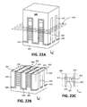
- FIG. 22A defines a location of a phantom plane that locates a cross-section of the structure of FIG. 21 for presentation in FIG. 22B ;
- FIG. 22B illustrates, in a perspective view, a cross-section of the structure of FIG. 21 taken along the phantom plane of FIG. 22A ;
- FIG. 22C shows detail of a portion of the cross-section of FIG. 22B ;
- FIG. 23 is a cross-sectional view of a semiconductor structure employing titanium nitride (TiN) as a thin protective conducting layer;
- FIG. 24 is a flowchart illustrating an implementation of a method described herein.
- FIG. 1 is a perspective view of a portion of a prior-art semiconductor structure at a manufacturing stage preparatory to formation of wordlines.
- the diagram includes x-y-z axes that may be used for spatial reference in this and other figures presented herein.
- the illustrated structure includes an oxide-nitride-oxide (ONO) layer 110 formed on a silicon substrate 100 , the ONO layer 110 being disposed under a polysilicon conducting structure 115 (PL 1 ).
- PL 1 115 and the ONO layer 110 are bounded by an oxide layer 105
- the ONO layer 110 , PL 1 115 and oxide layer 105 structures extend in a y-direction.
- the PL 1 115 and oxide 105 structures are covered with a polysilicon overlay 125 (PL 3 ).
- FIG. 2 is a cross-sectional view of the prior-art structure of FIG. 1 taken along a line 2 - 2 ′.
- the cross-section of the PL 1 115 structure has a tapered shape, the shape being narrower at the top thereof than at the bottom where the PL 1 115 meets the ONO layer 110 .
- FIG. 3 is a perspective view of the structure of FIG. 1 after a wordline etch that removes a portion of the PL 1 115 and the PL 3 125 from the structure.
- Illustrated wordlines 120 which are formed from remaining material of the PL 3 125 and remaining material of the PL 1 115 and separated by a space 135 , are intended to provide parallel conducting paths that provide electrical connections between external read/write hardware (not shown) and the ONO layer 110 .
- the wordlines 120 are required to be electrically isolated from each other.
- FIG. 4 illustrates a result of the wordline etch viewed in an x-z plane corresponding to the line 4 - 4 ′ ( FIG. 3 ).
- the wordline etch which may be an anisotropic etch as represented by dotted arrows 145 , removes portions of the PL 3 125 as well as a substantial portion of the PL 1 115 in a region defined by the space 135 ( FIG. 3 ), but may leave behind polysilicon material known as stringers, such as stringers 140 , on sidewalls of the space vacated by the PL 1 115 .
- the stringers 140 can provide unwanted conduction paths between parallel wordlines spaced in the y-direction (cf. FIG. 3 ), thereby creating serious defects that may create random single-bit errors in a memory product so affected.
- One prior-art approach to eliminating stringers is to change a profile of the PL 1 115 ( FIG. 2 ) to have a reentrant cross-section as illustrated by a PL 1 165 in FIG. 5 .
- reentrant is meant that the sidewalls of the PL 1 165 slope inwardly at the bottom of the profile of the PL 1 165 .
- the structure of FIG. 5 includes a substrate 150 , an ONO layer 160 , oxide 155 and an overlying PL 3 170 .
- an anisotropic etch 175 that removes polysilicon is applied to the structure of FIG. 5 as shown in FIG. 6 , no stringers remain.
- an upper dimension (measured in the x-direction) of the PL 1 165 is increased relative to a corresponding dimension in the structure of FIG. 2 , a change that can lead to instability in cell critical dimension (CD).
- CD cell critical dimension
- FIG. 7 A prior-art approach to mitigating the CD instability problem associated with the reentrant profile of FIGS. 5 and 6 is to create a vertical profile as illustrated in FIG. 7 .
- the structure illustrated in FIG. 7 is similar to those of FIGS. 1-6 , comprising a substrate 180 , an oxide layer 185 , an ONO layer 190 , a PL 1 195 having the vertical profile, and a polysilicon overlay PL 3 200 .
- a wordline etch 210 to remove portions of the PL 3 200 and the PL 1 195 may leave stringers 205 on sides of the space vacated by the etch, this excess polysilicon may be removed by performing an isotropic over-etch.
- the over-etch can, however, cause a loss of cell CD, corresponding to, for example, a line width 215 in FIG. 9 , a loss that cannot be tolerated when the wordline pitch shrinks to about 40 nm or less.
- the prior-art methods described above share a common approach, that of first depositing a polysilicon layer (e.g., PL 1 115 , 165 , and 195 , and PL 3 125 , 170 , and 200 in respective FIGS. 2 , 5 , and 7 ) and then etching to remove portions of the polysilicon in a wordline etch, as illustrated in FIGS. 3 , 4 , 6 , and 8 .
- a polysilicon layer e.g., PL 1 115 , 165 , and 195 , and PL 3 125 , 170 , and 200 in respective FIGS. 2 , 5 , and 7
- etching to remove portions of the polysilicon in a wordline etch, as illustrated in FIGS. 3 , 4 , 6 , and 8 .
- the present invention provides a novel approach to wordline formation, which approach may be referred to as a semi-damascene method of wordline formation, whereby openings are first created in a dielectric material (e.g., oxide) and then filled with polysilicon before etching to create wordlines.
- a dielectric material e.g., oxide
- FIGS. 10-16 One example of a method in accordance with the present invention may be described by referring to FIGS. 10-16 .
- FIG. 10 illustrates a collection of layers of materials well-known in the art of semiconductor manufacture viewed in cross-section along a y-axis (not visible) in an x-z plane.
- the layers, formed on a substrate 300 comprise a thin storage layer 305 , which may be formed, for example, of oxide-nitride-oxide (ONO), overlying the substrate 300 .
- the storage layer 305 has disposed thereon a thin protective layer, for example, a thin protective conducting layer 310 , that is formed, for example, of polycrystalline silicon, titanium nitride, amorphous silicon and/or the like, effectively replacing the PL 1 115 / 165 / 195 in the prior-art structures of FIGS.
- a dielectric layer 315 such as a layer of buffer oxide, may overlie the protective conducting layer 310 , and a sacrificed layer 320 formed, for example, of ceramic material, such as silicon nitride (SIN) (e.g., Si 3 N 4 ), may be disposed above the dielectric layer 315 .
- Si nitride Si 3 N 4
- the storage layer 305 when formed of ONO, for example, may have a thickness in typical examples ranging from about 150 ⁇ to about 250 ⁇ with a typical value of about 180 ⁇ .
- the protective conducting layer 310 may have a thickness in a range of about 100 ⁇ to about 200 ⁇ with a typical value being about 150 ⁇ .
- the dielectric layer 315 may have a thickness between about 50 ⁇ and about 150 ⁇ , with a typical value of about 100 ⁇ .
- the sacrificed layer 320 which may be used as a stop layer in later processing steps, may have a thickness in a range of about 300 ⁇ to about 700 ⁇ , with a typical value of about 500 ⁇ .
- the layers are patterned, for example, and are subjected to etching, to create openings that expose portions of the substrate.
- a BDF etch using one or more etchants such as CF4, CHF3, CH2F2, O2, N2, Ar, SF6, and the like may be performed on the layers 305 / 310 / 315 / 320 of FIG. 10 to create openings having a profile 325 as illustrated in FIG. 11 .
- a reentrant profile is illustrated in FIG. 11 . In other examples, the profile may not be reentrant.
- the protective conducting layer 310 may be very thin when compared, for example, with the thickness 130 of the corresponding prior-art PL 1 115 ( FIG. 2 ), a property that may aid in maintaining cell critical dimension (CD) uniformity, as is described below with reference to FIG. 14 .
- CD critical dimension
- the structure of FIG. 11 may be filled-in (i.e., deposited) with a dielectric material, for example, BD oxide 335 , and chemical mechanical planarization (CMP) may be employed to remove excess oxide.
- CMP chemical mechanical planarization
- the sacrificed layer 320 then may be removed without damaging the oxide layer 335 , the dielectric layer 315 or the thin protective conducting layer 310 by using, for example, hot phosphoric acid (H 3 PO 4 ).
- FIG. 13 illustrates a result of removal of the sacrificed layer 320 whereby openings 340 are created between regions of BD oxide 335 .
- the shape of the openings 340 in FIG. 13 may then be modified by using diluted hydrofluoric acid (HF) to pull-back the BD oxide 335 and to remove the buffer oxide layer 315 .
- HF diluted hydrofluoric acid
- FIG. 14 A result of this pull-back and removal is illustrated in FIG. 14 , wherein the thin protective conducting layer 310 remains substantially intact. That is, a width 330 (e.g., CD) of the protective conducting layer 310 may be well-controlled (i.e., approximately or substantially unaffected or only slightly affected by the removal of the sacrificed layer 320 , the BD oxide 335 , and the buffer oxide layer 315 ) when compared, for example, with an effect on the corresponding CD 215 in the prior art embodiment illustrated in FIG. 9 .
- the profile 325 illustrated in FIG. 11 may not be reentrant, and the width 330 may be greater than a width 331 of the storage layer 305 .
- FIG. 15 A perspective view of the structure of FIG. 14 is illustrated in FIG. 15 where the structure has been modified by filling-in with polysilicon 350 and by overlaying a hard mask layer 355 formed of, for example, oxide, nitride, oxy-nitride (SiO x N y , DARC), ACL (amorphous carbon layer), other materials which have high endurance during polysilicon etch, and the like.
- a hard mask layer 355 formed of, for example, oxide, nitride, oxy-nitride (SiO x N y , DARC), ACL (amorphous carbon layer), other materials which have high endurance during polysilicon etch, and the like.
- Wordlines 360 may be formed in the structure of FIG. 15 as illustrated in FIG. 16 by patterning and performing a wordline etch that removes hard mask material 355 and polysilicon material 350 to create a space 365 that defines wordlines 360 formed of remaining polysilicon material 350 .
- the polysilicon 350 of the wordlines makes electrical contact with the thin protective conducting layer 310 .
- the thin protective conducting layer 310 becomes part of the wordlines 360 thereby providing a conducting path between external read/write hardware (not shown) and the storage layer 305 .
- This conducting path may be electrically identical to that provided by wordlines 120 in, for example, the prior art structure of FIG. 3 , but without stringers, a consequence of the introduction of the bowl-shaped profile 345 shown in FIGS.
- FIG. 14 may comprise a memory device having an additional conducting layer (e.g., a floating gate (FG)) disposed between the storage (e.g., ONO) layer 305 and the substrate 300 .
- a gate structure e.g., a control gate
- the control gate may comprise a conductive gate layer connected with, and forming an electrical connection with, the thin protective conducting layer 310 . That is, the conductive gate layer and the thin protective conducting layer 310 may comprise a gate structure.
- the gate structure may comprise a damascene structure.
- the semi-damascene approach to wordline formation may integrate into standard (e.g., prior art) processes in a straightforward manner tabulated in Table 1.
- Table 1 an etch process used in PL 1 formation (cf. FIGS. 1-9 ) is replaced by a damascene process (cf. the gate structures illustrated in FIGS. 10-15 and modifications thereof described above), and wordline formation employs an etch step (cf. FIG. 16 ) in a manner similar to that of standard methods (cf. FIG. 3 ).
- the semi-damascene approach is similar in important ways to standard processes for wordline formation. Consequently, introducing the semi-damascene approach into existing process flows may advantageously be accomplished with minimal disruption to established practices.
- FIG. 17 is a perspective view of a semiconductor structure at an intermediate stage of manufacture comprising high-aspect-ratio trenches 400 extending in a y-direction formed from a semiconductor stack that may comprise, for example, a substrate 405 overlaid by alternating layers of polysilicon 425 and oxide 430 , and a SIN layer 435 .
- the structure may be overlaid with an ONO layer 410 , a thin protective conducting layer 415 , which may comprise polysilicon, and a dielectric (e.g., oxide) layer 420 .
- An etch step (e.g., a wordline etch) of the polysilicon/oxide may be performed in an x-direction to form a structure as illustrated in FIG. 18 .
- the structure of FIG. 18 may be filled-in with oxide 440 , with excess oxide 440 being removed by CMP, to yield the structure of FIG. 19 in which the oxide layer 420 effectively becomes part of the filled-in oxide 440 .
- a portion of the oxide layer 420 lying at the top surface of the structure of FIG. 18 is removed by the CMP process, which stops when the thin protective layer 415 is reached.
- a damascene etch performed on the structure of FIG. 19 may remove oxide material 440 to form the structure shown in FIG. 20 , wherein the thin protective conducting layer 415 protects the ONO layer 410 from being damaged during the etch.
- the resulting structure includes openings 433 (only one of which is illustrated in FIG. 20 for simplicity) in the oxide 440 formed by curved profiles 430 that may be analogous to the bowl-shaped profile 345 of FIGS. 14-16 .
- FIG. 20 may be filled-in with polysilicon 445 as shown in FIG. 21 .
- An internal view of the structure of FIG. 21 may be seen by slicing the structure with a phantom x-y plane 450 ( FIG. 22A ). When the portion of FIG. 22A above the plane 450 is removed, a bottom portion of the structure may appear as shown in FIG. 22B .
- the fill-in with polysilicon is noted to form polysilicon plugs 455 .
- a detailed representation of a portion 460 of the structure of FIG. 22B viewed in a z-direction, i.e., in an x-y plane, is shown in FIG. 22C .
- the structure is noted to comprise a polysilicon plug 455 that makes electrical contact with a winged ONO strip 410 through the thin protective conducting layer 415 .
- FIG. 24 One implementation of the method described herein may be summarized in a flowchart as illustrated in FIG. 24 .
- the implementation described in the figure commences at step 500 by providing a semiconductor stack that includes a storage layer formed over a substrate.
- a thin protective conducting layer may overlie the storage layer, and additional layers of dielectric and ceramic material may be disposed above the storage layer.
- An example of such a semiconductor stack is shown in FIG. 10 , describing a storage layer 305 (e.g., a charge storage layer) formed of, for example, oxide-nitride-oxide (ONO) disposed on a substrate 300 with a thin protective conducting layer 310 of, for example, polycrystalline silicon that overlies the storage layer 305 .
- a storage layer 305 e.g., a charge storage layer
- ONO oxide-nitride-oxide
- a dielectric layer of buffer oxide 315 is deposited on the protective conducting layer 310 , and a sacrificed layer 320 is overlaid onto the buffer oxide layer 315 .
- the sacrificed layer 320 comprises, according to one example, silicon nitride (e.g., Si 3 N 4 ).
- a BDF etch which may employ (an) etchant(s) such as CF4/CHF3/CH2F2/O2/N2/Ar/SF6 and, the like, may be performed at step 505 on the semiconductor stack in order to form openings into which polysilicon may be deposited in a later step.
- An exemplary result of such an etch is illustrated in FIG. 11 , wherein openings 325 are formed.
- Dielectric material such as BD oxide 335 ( FIG. 12 ) may be deposited over the structure at step 510 , thereby filling in the openings 325 ; CMP may be performed at step 515 to remove excess BD oxide, the CMP operation stopping when the sacrificed layer 320 is reached.
- remaining portions of the sacrificed layer 320 may be removed at step 520 by etching with hot phosphoric acid (H 3 PO 4 ).
- the removal may create openings 340 that expose the buffer oxide layer 315 without damaging the buffer oxide layer 315 , the protective conducting layer 310 , or the storage layer 305 .
- the openings 340 may be modified by pulling back the BD oxide using diluted hydrofluoric acid (HF) at step 525 .
- the storage layer 305 e.g., an ONO layer
- the thin protective conducting layer 310 e.g., a polysilicon layer.
- the structure so formed then may be filled-in with conducting material (e.g., polysilicon) 350 ( FIG. 15 ) at step 530 , and a hard mask 355 , which may comprise, for example, such materials as identified previously, may be deposited over the layer of conducting material 350 at step 535 .
- conducting material e.g., polysilicon
- a hard mask 355 which may comprise, for example, such materials as identified previously, may be deposited over the layer of conducting material 350 at step 535 .
- a wordline etch may be performed at step 540 using etchant(s) such as HBr/Cl2/O2/N2/Ar and the like as illustrated, for example, in FIG. 16 .
- etchant(s) such as HBr/Cl2/O2/N2/Ar and the like as illustrated, for example, in FIG. 16 .
- loss of wordline polysilicon may be minimized by this process.
- the thin protective conducting layer described above may be replaced by other conducting materials.
- the thin protective conducting layer may comprise tungsten silicide (WSi) or cobalt silicide (CoSi) in front-end-of-line (FEOL) and/or middle-end-of-line (MEOL) processes.
- the protective conducting layer may comprise titanium nitride (TiN) as described in FIG.
- the thin protective conducting layer may be formed of polysilicon and/or amorphous silicon.
- any damascene process having a thin conductor existing before damascene formation with the thin conductor subsequently connecting to filled material is included in the scope of the description provided herein.
- the semi-damascene process referred to above may be used with any semiconductor structure, including such examples as a line pattern, a hole pattern, a self-aligned contact and/or a vertical device structure.
- the intent accompanying this disclosure is to have such embodiments construed in conjunction with the knowledge of one skilled in the art to cover all modifications, variations, combinations, permutations, omissions, substitutions, alternatives, and equivalents of the embodiments, to the extent not mutually exclusive, as may fall within the spirit and scope of the invention as limited only by the appended claims.
Landscapes
- Engineering & Computer Science (AREA)
- Microelectronics & Electronic Packaging (AREA)
- Power Engineering (AREA)
- Physics & Mathematics (AREA)
- Condensed Matter Physics & Semiconductors (AREA)
- General Physics & Mathematics (AREA)
- Computer Hardware Design (AREA)
- Ceramic Engineering (AREA)
- Manufacturing & Machinery (AREA)
- Chemical & Material Sciences (AREA)
- Geometry (AREA)
- Chemical Kinetics & Catalysis (AREA)
- General Chemical & Material Sciences (AREA)
- Inorganic Chemistry (AREA)
- Semiconductor Memories (AREA)
- Non-Volatile Memory (AREA)
- Internal Circuitry In Semiconductor Integrated Circuit Devices (AREA)
Abstract
Description
| TABLE 1 | |
| Approaches to Wordline | |
| Formation | |
| Semi- | |||
| STD | Damascene | Damascene | |
| PL1 formation | Etch | Damascene | Damascene |
| WL formation | Etch | Damascene | Etch |
| Compatible to STD | — | X | O |
| process flow | |||
| Difficulty and | — | High | ~STD |
| Complexity | |||
| Cost compared to | — | Higher | ~STD |
| STD process | |||
| (1) —: Standard (STD) condition; | |||
| (2) ~STD: Close to standard condition; | |||
| (3) X: No (Needs many modifications); and | |||
| (4) O: Yes (compatible to STD process flow without any Modification). | |||
Claims (8)
Priority Applications (3)
| Application Number | Priority Date | Filing Date | Title |
|---|---|---|---|
| US14/493,021 US9252153B1 (en) | 2014-09-22 | 2014-09-22 | Method of word-line formation by semi-damascene process with thin protective conductor layer |
| TW104105426A TWI555133B (en) | 2014-09-22 | 2015-02-16 | Method of word-line formation by semi-damascene process with thin protective conductor layer |
| CN201510108359.5A CN106033740A (en) | 2014-09-22 | 2015-03-12 | Method for manufacturing word-line, method for forming semiconductor element, and memory element |
Applications Claiming Priority (1)
| Application Number | Priority Date | Filing Date | Title |
|---|---|---|---|
| US14/493,021 US9252153B1 (en) | 2014-09-22 | 2014-09-22 | Method of word-line formation by semi-damascene process with thin protective conductor layer |
Publications (1)
| Publication Number | Publication Date |
|---|---|
| US9252153B1 true US9252153B1 (en) | 2016-02-02 |
Family
ID=55175034
Family Applications (1)
| Application Number | Title | Priority Date | Filing Date |
|---|---|---|---|
| US14/493,021 Active US9252153B1 (en) | 2014-09-22 | 2014-09-22 | Method of word-line formation by semi-damascene process with thin protective conductor layer |
Country Status (3)
| Country | Link |
|---|---|
| US (1) | US9252153B1 (en) |
| CN (1) | CN106033740A (en) |
| TW (1) | TWI555133B (en) |
Families Citing this family (1)
| Publication number | Priority date | Publication date | Assignee | Title |
|---|---|---|---|---|
| CN112449724A (en) * | 2020-10-12 | 2021-03-05 | 长江先进存储产业创新中心有限责任公司 | Novel self-aligned semi-damascene contact scheme for reducing cost for 3D PCM |
Citations (7)
| Publication number | Priority date | Publication date | Assignee | Title |
|---|---|---|---|---|
| US20060292781A1 (en) * | 2005-06-23 | 2006-12-28 | Samsung Electronics Co., Ltd. | Finfets, nonvolatile memory devices including finfets, and methods of forming the same |
| US20070018201A1 (en) * | 2005-07-22 | 2007-01-25 | Michael Specht | Non-volatile memory cells and methods for fabricating non-volatile memory cells |
| US20070158736A1 (en) * | 2005-12-28 | 2007-07-12 | Kabushiki Kaisha Toshiba | Semiconductor memory device and method of fabricating the same |
| US20070267676A1 (en) * | 2006-05-22 | 2007-11-22 | Samsung Electronics Co., Ltd. | Fin field effect transistor and method for forming the same |
| US20090321816A1 (en) * | 2008-06-27 | 2009-12-31 | Samsung Electronics Co., Ltd. | Vertical-type non-volatile memory device |
| US20120139030A1 (en) * | 2009-06-12 | 2012-06-07 | Kiwamu Sakuma | Nonvolatile semiconductor memory |
| US20130015519A1 (en) * | 2010-03-19 | 2013-01-17 | Shosuke Fujii | Nonvolatile semiconductor memory device and method of manufacturing the same |
Family Cites Families (5)
| Publication number | Priority date | Publication date | Assignee | Title |
|---|---|---|---|---|
| KR100341480B1 (en) * | 2000-05-26 | 2002-06-21 | 윤종용 | Method for self-aligned shallow trench isolation |
| KR100375235B1 (en) * | 2001-03-17 | 2003-03-08 | 삼성전자주식회사 | Sonos flash memory device and a method for fabricating the same |
| KR100395759B1 (en) * | 2001-07-21 | 2003-08-21 | 삼성전자주식회사 | Non-volatile memory device and method of fabricating the same |
| KR100643542B1 (en) * | 2005-03-16 | 2006-11-10 | 삼성전자주식회사 | Non-volatile memory device having a charge trap layer and fabrication method thereof |
| KR100799030B1 (en) * | 2006-06-28 | 2008-01-28 | 주식회사 하이닉스반도체 | Method of manufacturing a NAND flash memory device |
-
2014
- 2014-09-22 US US14/493,021 patent/US9252153B1/en active Active
-
2015
- 2015-02-16 TW TW104105426A patent/TWI555133B/en active
- 2015-03-12 CN CN201510108359.5A patent/CN106033740A/en active Pending
Patent Citations (7)
| Publication number | Priority date | Publication date | Assignee | Title |
|---|---|---|---|---|
| US20060292781A1 (en) * | 2005-06-23 | 2006-12-28 | Samsung Electronics Co., Ltd. | Finfets, nonvolatile memory devices including finfets, and methods of forming the same |
| US20070018201A1 (en) * | 2005-07-22 | 2007-01-25 | Michael Specht | Non-volatile memory cells and methods for fabricating non-volatile memory cells |
| US20070158736A1 (en) * | 2005-12-28 | 2007-07-12 | Kabushiki Kaisha Toshiba | Semiconductor memory device and method of fabricating the same |
| US20070267676A1 (en) * | 2006-05-22 | 2007-11-22 | Samsung Electronics Co., Ltd. | Fin field effect transistor and method for forming the same |
| US20090321816A1 (en) * | 2008-06-27 | 2009-12-31 | Samsung Electronics Co., Ltd. | Vertical-type non-volatile memory device |
| US20120139030A1 (en) * | 2009-06-12 | 2012-06-07 | Kiwamu Sakuma | Nonvolatile semiconductor memory |
| US20130015519A1 (en) * | 2010-03-19 | 2013-01-17 | Shosuke Fujii | Nonvolatile semiconductor memory device and method of manufacturing the same |
Also Published As
| Publication number | Publication date |
|---|---|
| CN106033740A (en) | 2016-10-19 |
| TWI555133B (en) | 2016-10-21 |
| TW201613034A (en) | 2016-04-01 |
Similar Documents
| Publication | Publication Date | Title |
|---|---|---|
| US11114550B2 (en) | Recessing STI to increase FIN height in FIN-first process | |
| US11600636B2 (en) | Stacked connections in 3D memory and methods of making the same | |
| US9349837B2 (en) | Recessing STI to increase Fin height in Fin-first process | |
| US10763169B2 (en) | Contact structure and associated method for flash memory | |
| US8623727B2 (en) | Method for fabricating semiconductor device with buried gate | |
| US11195853B2 (en) | Contact structures having conductive portions in substrate in three-dimensional memory devices and methods for forming the same | |
| US11792980B2 (en) | Contact structures having conductive portions in substrate in three-dimensional memory devices and methods for forming the same | |
| TW202147579A (en) | Staircase structure in three-dimensional memory device and method for forming the same | |
| US20160020119A1 (en) | Method of Controlling Recess Depth and Bottom ECD in Over-Etching | |
| CN112635659B (en) | Semiconductor structure and forming method thereof | |
| US20180233451A1 (en) | Pad structure and method for fabricating the same | |
| US9252153B1 (en) | Method of word-line formation by semi-damascene process with thin protective conductor layer | |
| US9269618B2 (en) | Semiconductor device and method for manufacturing the same | |
| US9224803B2 (en) | Formation of a high aspect ratio contact hole | |
| CN116171045A (en) | Three-dimensional memory device having isolation structure for source selection gate line and method for forming the same | |
| US9337048B2 (en) | Method for disconnecting polysilicon stringers during plasma etching | |
| CN105280590B (en) | Semiconductor structure and its manufacturing method | |
| TWI518802B (en) | Method of fabricating semiconductor device | |
| US11488977B2 (en) | Three-dimensional memory devices and methods for forming the same | |
| US20070010089A1 (en) | Method of forming bit line of semiconductor device | |
| KR20220145124A (en) | Integrated Circuit devices and manufacturing methods for the same | |
| TWI470700B (en) | Semiconductor device and manufacturing method thereof | |
| TW201707167A (en) | Connector structure and method for fabricating the same |
Legal Events
| Date | Code | Title | Description |
|---|---|---|---|
| AS | Assignment |
Owner name: MACRONIX INTERNATIONAL CO., LTD., TAIWAN Free format text: ASSIGNMENT OF ASSIGNORS INTEREST;ASSIGNORS:LUNG, CHENG-YI;WEI, AN-CHYI;YANG, TA-HUNG;SIGNING DATES FROM 20140905 TO 20140909;REEL/FRAME:033790/0979 |
|
| STCF | Information on status: patent grant |
Free format text: PATENTED CASE |
|
| MAFP | Maintenance fee payment |
Free format text: PAYMENT OF MAINTENANCE FEE, 4TH YEAR, LARGE ENTITY (ORIGINAL EVENT CODE: M1551); ENTITY STATUS OF PATENT OWNER: LARGE ENTITY Year of fee payment: 4 |
|
| MAFP | Maintenance fee payment |
Free format text: PAYMENT OF MAINTENANCE FEE, 8TH YEAR, LARGE ENTITY (ORIGINAL EVENT CODE: M1552); ENTITY STATUS OF PATENT OWNER: LARGE ENTITY Year of fee payment: 8 |