WO2011111166A1 - ウエハ加工用フィルム及びウエハ加工用フィルムを用いて半導体装置を製造する方法 - Google Patents
ウエハ加工用フィルム及びウエハ加工用フィルムを用いて半導体装置を製造する方法 Download PDFInfo
- Publication number
- WO2011111166A1 WO2011111166A1 PCT/JP2010/053879 JP2010053879W WO2011111166A1 WO 2011111166 A1 WO2011111166 A1 WO 2011111166A1 JP 2010053879 W JP2010053879 W JP 2010053879W WO 2011111166 A1 WO2011111166 A1 WO 2011111166A1
- Authority
- WO
- WIPO (PCT)
- Prior art keywords
- adhesive layer
- film
- wafer
- pressure
- wafer processing
- Prior art date
- Legal status (The legal status is an assumption and is not a legal conclusion. Google has not performed a legal analysis and makes no representation as to the accuracy of the status listed.)
- Ceased
Links
Images



Classifications
-
- H—ELECTRICITY
- H10—SEMICONDUCTOR DEVICES; ELECTRIC SOLID-STATE DEVICES NOT OTHERWISE PROVIDED FOR
- H10P—GENERIC PROCESSES OR APPARATUS FOR THE MANUFACTURE OR TREATMENT OF DEVICES COVERED BY CLASS H10
- H10P72/00—Handling or holding of wafers, substrates or devices during manufacture or treatment thereof
- H10P72/04—Apparatus for manufacture or treatment
- H10P72/0442—Apparatus for placing on an insulating substrate, e.g. tape
-
- H—ELECTRICITY
- H10—SEMICONDUCTOR DEVICES; ELECTRIC SOLID-STATE DEVICES NOT OTHERWISE PROVIDED FOR
- H10W—GENERIC PACKAGES, INTERCONNECTIONS, CONNECTORS OR OTHER CONSTRUCTIONAL DETAILS OF DEVICES COVERED BY CLASS H10
- H10W72/00—Interconnections or connectors in packages
- H10W72/071—Connecting or disconnecting
-
- H—ELECTRICITY
- H10—SEMICONDUCTOR DEVICES; ELECTRIC SOLID-STATE DEVICES NOT OTHERWISE PROVIDED FOR
- H10P—GENERIC PROCESSES OR APPARATUS FOR THE MANUFACTURE OR TREATMENT OF DEVICES COVERED BY CLASS H10
- H10P95/00—Generic processes or apparatus for manufacture or treatments not covered by the other groups of this subclass
Definitions
- the present invention relates to a wafer processing film, and more particularly to a wafer processing film including a dicing die bonding film having two functions of a dicing tape and a die bonding film.
- the present invention also relates to a method of manufacturing a semiconductor device using the wafer processing film.
- a dicing tape for fixing a semiconductor wafer when the semiconductor wafer is cut and separated into individual semiconductor chips (dicing), and for bonding the cut semiconductor chip to a lead frame, a package substrate, or the like, or
- a dicing die bonding film having both functions of a die bonding film (also referred to as a die attach film) for laminating and bonding semiconductor chips has been developed.
- Some of these dicing / die bonding films have been pre-cut in consideration of workability such as attachment to a semiconductor wafer and attachment to a ring frame during dicing.
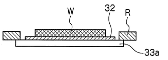
- the adhesive layer 32 and the circular label portion 33a of the pressure-sensitive adhesive film 33 are laminated with their centers aligned, and the circular label portion 33a of the pressure-sensitive adhesive film 33 covers the adhesive layer 32 and is released from the periphery thereof. It is in contact with the film 31.
- the dicing / die bonding film 35 is configured by a laminated structure including the adhesive layer 32 and the circular label portion 33 a of the adhesive film 33.
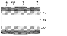
- the wafer processing film 30 as described above is thicker than the other portions where the adhesive layer 32 and the circular label portion 33 a of the adhesive film 33 are laminated.
- the exposed release film 31 part between the circular label part 33a and the peripheral part 33b is a part from which the adhesive film 33 has been removed, and the adhesive film between the adhesive film 33 (33a, 33b) part.
- the film 30 for wafer processing is distribute
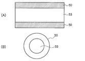
- FIG. 7 shows an example of a winding core 50 in which a cylindrical cavity 53 is formed at the center of rotation. Therefore, as shown in FIG.
- Patent Document 1 in order to suppress generation
- the adhesive sheet of Patent Document 1 is provided with a support layer, so that the winding pressure applied to the adhesive sheet is dispersed or collected in the support layer to suppress the generation of transfer marks.
- the support layer is formed on a part other than the adhesive layer and the pressure-sensitive adhesive film required when manufacturing a semiconductor device on the release substrate, the support layer The width of the support layer is limited with respect to the outer diameter of the adhesive layer and the pressure-sensitive adhesive film, and the effect of suppressing the label traces is not sufficient. Also, since the support layer is generally not sticky and does not adhere well to the release substrate (PET film), it floats from the release substrate at the narrowest part of the support layer, and is diced to the semiconductor wafer. When the die bonding film is bonded, the above-described floating portion is caught by the apparatus, causing a problem that the semiconductor wafer is damaged.
- the object of the present invention is to sufficiently suppress the generation of transfer marks on the adhesive layer when a wafer processing film including a dicing die bonding film having an adhesive layer and an adhesive film is rolled up.
- An object of the present invention is to provide a film for wafer processing that can be used.
- Another object of the present invention is to provide a method of manufacturing a semiconductor device using such a wafer processing film.
- a film for wafer processing includes a base film, an adhesive film comprising an adhesive layer provided on the base film, and An adhesive layer provided on the pressure-sensitive adhesive layer, and the pressure-sensitive adhesive layer includes a radiation polymerizable compound and one photoinitiator at least at a position corresponding to the ring frame, and the one photoinitiator
- the wavelength of the light that contains the radiation polymerizable compound and the other photoinitiator at a position other than the part containing the agent, and the one photoinitiator reacts with the wavelength of the light that the other photoinitiator reacts with. It is characterized by being different.
- the pressure-sensitive adhesive layer contains a photoinitiator that reacts to different wavelengths at least in the part corresponding to the ring frame and the other part.
- a photoinitiator that reacts to different wavelengths at least in the part corresponding to the ring frame and the other part.
- the film for wafer processing which concerns on the 2nd aspect of this invention was provided on the adhesive film which consists of a base film, the adhesive layer provided on the said base film, and the said adhesive layer
- An adhesive layer, and the pressure-sensitive adhesive layer includes at least one of a radiation polymerizable compound and a heat polymerizable compound in a portion corresponding to the ring frame, and includes one of the radiation polymerizable compound and the heat polymerizable compound.
- the other part of the radiation polymerizable compound and the thermally polymerizable compound is included in a part other than the part to be included.
- the portion corresponding to the ring frame of the pressure-sensitive adhesive layer when at least a portion corresponding to the ring frame of the pressure-sensitive adhesive layer contains a radiation polymerizable compound, the portion corresponding to the ring frame is cured by irradiating the pressure-sensitive adhesive layer with radiation.
- the adhesive strength can be reduced and the adhesive layer corresponding to the cured part can be peeled off.
- the semiconductor wafer and the adhesive layer can be peeled off from the pressure-sensitive adhesive layer and picked up by thermal polymerization and curing. it can.
- the pressure-sensitive adhesive force is reduced by thermal polymerization and curing, and the adhesive layer corresponding to the cured portion can be peeled off. it can. Since at least the portion other than the portion corresponding to the ring frame contains a radiation polymerizable compound, the adhesive layer is irradiated with radiation, and at least the portion other than the portion corresponding to the ring frame is cured, and the semiconductor wafer and The adhesive layer can be separated from the pressure-sensitive adhesive layer and picked up.
- the wafer processing film according to the third aspect of the present invention is the above-described wafer processing film according to the first or second aspect of the present invention, wherein the adhesive layer is precut into a shape corresponding to the semiconductor wafer.
- the pressure-sensitive adhesive layer is not precut into a shape corresponding to the ring frame.
- the adhesive layer and the pressure-sensitive adhesive layer are not pre-cut, when the film for wafer processing is wound into a roll as a product, the adhesive layer and the pressure-sensitive adhesive layer are generated in the laminated portion of the adhesive layer and the pressure-sensitive adhesive film. Since there is no step, transfer marks can be prevented from being generated in the adhesive layer.
- the wafer processing film according to the fourth aspect of the present invention is the above-described wafer processing film according to any one of the first to third aspects of the present invention, wherein the adhesive layer corresponds to at least a semiconductor wafer.
- a cut is provided outside the position corresponding to the ring frame and inside the position corresponding to the ring frame.
- the pressure-sensitive adhesive layer corresponding to the ring frame is cured, thereby reducing the adhesive force and bonding from the cured part of the pressure-sensitive adhesive layer based on the notch.
- the agent layer can be peeled off.
- a method for manufacturing a semiconductor device according to the first aspect of the present invention is a method for manufacturing a semiconductor device using the wafer processing film according to any one of the first to fourth aspects of the present invention described above.
- Corresponding to a wafer bonding step a step of fixing the ring frame to the pressure-sensitive adhesive layer, a step of dicing the wafer to form individual chips and an adhesive layer, and a pressure-sensitive adhesive layer wafer Curing the portion and picking up the singulated chip and the adhesive layer.
- a portion corresponding to the ring frame and a portion corresponding to the semiconductor wafer of the pressure-sensitive adhesive layer other than a portion corresponding to the semiconductor wafer of the pressure-sensitive adhesive layer can be cured stepwise to reduce the adhesive strength of the pressure-sensitive adhesive layer and change the peelable position between the adhesive layer and the pressure-sensitive adhesive layer. Therefore, the design of the desired semiconductor device can be changed without a large-scale change of the existing equipment.
- the adhesive layer and the pressure-sensitive adhesive layer do not need to be pre-cut with respect to the wafer processing film before manufacturing the semiconductor device. In this case, since there is no level difference generated in the laminated portion of the adhesive layer and the pressure-sensitive adhesive film, it is possible to prevent transfer marks from being generated in the adhesive layer.
- the pressure-sensitive adhesive layer contains a photoinitiator that reacts to different wavelengths at least in a portion corresponding to the ring frame and in other portions.
- a photoinitiator that reacts to different wavelengths at least in a portion corresponding to the ring frame and in other portions.
- the pressure-sensitive adhesive layer when at least a portion corresponding to the ring frame of the pressure-sensitive adhesive layer contains a radiation polymerizable compound, the pressure-sensitive adhesive layer is irradiated with radiation so that the at least The part corresponding to the ring frame is cured to reduce the adhesive force, and the adhesive layer corresponding to the cured part can be peeled off. And since at least a portion other than the portion corresponding to the ring frame contains a thermopolymerizable compound, the semiconductor wafer and the adhesive layer can be peeled off from the pressure-sensitive adhesive layer and picked up by thermal polymerization and curing. it can.
- the pressure-sensitive adhesive force is reduced by thermal polymerization and curing, and the adhesive layer corresponding to the cured portion can be peeled off. it can. Since at least the portion other than the portion corresponding to the ring frame contains a radiation polymerizable compound, the adhesive layer is irradiated with radiation, and at least the portion other than the portion corresponding to the ring frame is cured, and the semiconductor wafer and The adhesive layer can be separated from the pressure-sensitive adhesive layer and picked up.
- the adhesive layer and the pressure-sensitive adhesive layer are not pre-cut, when the wafer processing film is wound into a roll as a product, Since there is no level difference generated in the laminated portion with the pressure-sensitive adhesive film, it is possible to prevent transfer marks from being generated in the adhesive layer. Accordingly, it is possible to prevent a decrease in the adhesion between the adhesive layer and the semiconductor wafer due to air being caught between the adhesive layer and the semiconductor wafer, and to attach the semiconductor chip to a lead frame, a package substrate, or another semiconductor. When adhering to a chip, it is possible to prevent adhesion failure and problems during processing of a semiconductor wafer.
- the pressure-sensitive adhesive layer corresponding to the ring frame is cured, thereby reducing the adhesive force and curing the pressure-sensitive adhesive layer based on the notch.
- the adhesive layer can be peeled from the applied portion.
- Corresponding portions can be cured stepwise to reduce the adhesive strength of the pressure-sensitive adhesive layer, and the peelable position can be changed between the adhesive layer and the pressure-sensitive adhesive layer. Therefore, the design of the desired semiconductor device can be changed without a large-scale change of the existing equipment.
- FIG. 1 is a cross-sectional view of a wafer processing film according to the present embodiment.
- 2 and 3 are views for explaining a method of manufacturing a semiconductor device using the wafer processing film according to this embodiment.
- a wafer processing film 10 includes a base film 11 and an adhesive film 14 including an adhesive layer 12 provided on the base film 11, and an adhesive.
- a dicing die bonding film 15 having an adhesive layer 13 provided on the layer 12.
- the adhesive layer 13 is not pre-cut into a shape corresponding to a semiconductor wafer (or called a wafer), and the pressure-sensitive adhesive layer 12 is not pre-cut into a shape corresponding to the ring frame.
- the pressure-sensitive adhesive layer 12 and the adhesive layer 13 are laminated in a long shape on the base film 11 in the same manner as the base film 11, and the wafer processing film 10 has a thickness. Does not have different parts.
- the pressure-sensitive adhesive layer 12 contains a radiation polymerizable compound and two types of photoinitiators having different wavelengths of light to react.
- a release film which is a protective film (not shown), is attached to the entire surface of the adhesive layer 13 and distributed as a wafer processing film 10 to the market.
- the release film, the adhesive layer 13, and the pressure-sensitive adhesive film 14 including the base film 11 and the pressure-sensitive adhesive layer 12, which are components of the wafer processing film 10 will be described.
- release film As the release film used for the wafer processing film 10, a known film such as a polyethylene terephthalate (PET) type, a polyethylene type, or a film subjected to a release treatment can be used.
- PET polyethylene terephthalate
- the thickness of the release film is not particularly limited and may be set appropriately, but is preferably 25 to 50 ⁇ m.
- the adhesive layer 13 is peeled off from the adhesive film 14 and attached to the chip when picking up an individual semiconductor chip (or called a chip) after the semiconductor wafer or the like is bonded and diced. It is used as an adhesive when fixing a chip to a substrate or a lead frame. Therefore, the adhesive layer 13 has releasability that can be peeled off from the pressure-sensitive adhesive film 14 while being attached to the separated chip when picking up the chip. In order to bond and fix the chip to the substrate or the lead frame, it has sufficient adhesion reliability.
- the adhesive layer 13 is obtained by forming a film of an adhesive in advance.
- a known polyimide resin, polyamide resin, polyetherimide resin, polyamideimide resin, polyester resin, polyester resin, or polyesterimide used for the adhesive is used.
Landscapes
- Dicing (AREA)
- Adhesives Or Adhesive Processes (AREA)
Abstract
Description
以下、本発明の第1実施形態に係るウエハ加工用フィルムの各構成要素について詳細に説明する。本発明の第1実施形態に係るウエハ加工用フィルム10は、図1に示すように、基材フィルム11及び基材フィルム11上に設けられた粘着剤層12からなる粘着フィルム14と、粘着剤層12上に設けられた接着剤層13とを有するダイシング・ダイボンディングフィルム15である。また、接着剤層13は、半導体ウエハ(または、ウエハと呼ぶ)に対応した形状にプリカットされておらず、粘着剤層12は、リングフレームに対応した形状にプリカットされていない。本実施形態においては、粘着剤層12及び接着剤層13は、基材フィルム11上に、基材フィルム11と同様に長尺状に積層されており、ウエハ加工用フィルム10は、厚さが異なる部分を有していない。また、粘着剤層12には、放射線重合性化合物と、反応する光の波長が異なる2種類の光開始剤が含まれている。
ウエハ加工用フィルム10に用いられる離型フィルムとしては、ポリエチレンテレフタレート(PET)系、ポリエチレン系、その他、離型処理がされたフィルム等周知のものを使用することができる。離型フィルムの厚さは、特に限定されるものではなく、適宜に設定してよいが、25~50μmが好ましい。
接着剤層13は、半導体ウエハ等が貼り合わされてダイシングされた後、個片化された半導体チップ(または、チップと呼ぶ)をピックアップする際に、粘着フィルム14から剥離してチップに付着し、チップを基板やリードフレームに固定する際の接着剤として使用されるものである。従って、接着剤層13は、チップをピックアップする際に、個片化されたチップに付着したままの状態で、粘着フィルム14から剥離することができる剥離性を有し、さらに、ダイボンディングする際において、チップを基板やリードフレームに接着固定するために、十分な接着信頼性を有するものである。
本実施形態に係る粘着フィルム14は、基材フィルム11に粘着剤層12を設けたものである。そして、粘着フィルム14は、ウエハをダイシングする際にはウエハが剥離しないように十分な粘着力を有し、ダイシング後にチップをピックアップする際には容易に接着剤層13から剥離できるよう低い粘着力を有するものである。また、本実施形態に係るウエハ加工用フィルム10は、接着剤層13のリングフレームに対応する位置がプリカットされていないため、リングフレーム装着前に、接着剤層13のリングフレームに対応する位置を含む部分の下に位置する粘着剤層12の粘着力を低くする必要がある。そのため、粘着フィルム14の粘着剤層12は、ウエハに対応する部分以外の部分に、放射線重合性化合物と一の光開始剤とが含まれており、一の光開始剤を含む箇所以外の部分すなわちウエハに対応する部分に、放射線重合性化合物と他の光開始剤とを含まれている。なお、ウエハに対応する部分以外の部分は、リングフレームに対応する位置を含む部分であるが、リングフレームに対応する部分にのみ一の光開始剤が含まれるようにし、それ以外の部分には他の光開始剤が含まれるようにしてもよい。
本発明の第2実施形態に係るウエハ加工用フィルムは、本発明の第1実施形態に係るウエハ加工用フィルム10(図1参照)と同様、基材フィルム(図1の符号11に相当)及び基材フィルム上に設けられた粘着剤層(図1の符号12に相当)からなる粘着フィルム(図1の符号14に相当)と、粘着剤層上に設けられた接着剤層(図1の符号13に相当)とを有するものであり、接着剤層は半導体ウエハに対応した形状にプリカットされておらず、粘着剤層もリングフレームに対応した形状にプリカットされていない。また、接着剤層には、少なくとも半導体ウエハに対応する位置よりも外側であってリングフレームに対応する位置よりも内側に切り込みが設けられている。なお、粘着剤層及び接着剤層は、基材フィルム上に、基材フィルムと同様に長尺状に積層されており、ウエハ加工用フィルムは、厚さが異なる部分を有していない。
第1実施形態に係るウエハ加工用フィルム10を用いて半導体装置を製造する方法を、図2及び図3を用いて説明する。図2及び図3は第1実施形態に係るウエハ加工用フィルム10を用いて半導体装置を製造する方法を説明する図であって、図2(A)は離型フィルム16が接着剤層13上に貼り付けられている状態を示すウエハ加工用フィルムの断面図であり、図2(B)は粘着剤層12の一部を硬化させ、硬化させた粘着剤層部分12a上の接着剤層13を剥離させた状態を示すウエハ加工用フィルムの断面図である。また、図2(C)はウエハWがウエハ加工用フィルムに貼り付けられた状態を示すウエハ及びウエハ加工用フィルムの断面図であり、図2(D)はウエハがダイシングされた状態を示すウエハ及びウエハ加工用フィルムの断面図であり、図2(E)はウエハに対応する位置の粘着剤層部分12bを硬化させた状態を示すウエハ及びウエハ加工用フィルムの断面図である。さらに、図3(A)はダイシングされたウエハが貼り合わされたウエハ加工用フィルムをエキスパンド装置に搭載した状態のウエハ及びウエハ加工用フィルムを示す断面図であり、図3(B)はエキスパンド後のウエハ及びウエハ加工用フィルムを示す断面図である。
図2(A)に示すように、まず、基材フィルム11及び基材フィルム11上に設けられた粘着剤層12からなる粘着フィルム14と、図示しないウエハの外周に対応した位置に切り込み13aが設けられている接着剤層13とを有するダイシング・ダイボンディングフィルム15に対して、接着剤層13側から離型フィルム16が貼り付けられているウエハ加工用フィルムを準備する。ウエハ加工用フィルムは、接着剤層13等がプリカットされていないことから、離型フィルム16が貼り合わされた製品としてロール状に巻いた際、接着剤層13と粘着フィルム14との積層部分に生じていた段差も存在しないため、接着剤層13に転写痕が発生することを防止することができる。
次に、一の光開始剤、すなわち、粘着剤層12のウエハに対応する部分以外に含まれる光開始剤が反応する波長(「波長A」と称する)の紫外線を、粘着剤層12に照射して硬化させる。硬化した部分12aの粘着力が低下するため、図2(B)に示すように、ウエハ加工用フィルムから離型フィルム16を剥がすとともに、接着剤層13の切り込み13aを基点として、硬化した粘着剤層部分12a上の接着剤層13のみを剥離することができる。
次に、図2(C)に示すように、硬化した粘着剤層部分12aの所定位置にリングフレーム20を貼り合わせ、ダイシング・ダイボンディングフィルム15の接着剤層13側から、接着剤層13に対して半導体ウエハWの裏面を貼り合わせる。なお、以後の工程において、リングフレーム20及び半導体ウエハWを長尺状のダイシング・ダイボンディングフィルム15に貼り合わせた状態で各工程を搬送させるのではなく、リングフレーム20及び半導体ウエハWを1組ずつ個別に搬送させる場合には、リングフレーム20を貼り合わせる前あるいは貼り合わせた後に、リングフレーム20の外周に沿って、ダイシング・ダイボンディングフィルム15を切断するとよい。
リングフレーム20を介してウエハ加工用フィルムをダイシング装置(図示せず)に固定し、ブレードを用いて、半導体ウエハWを機械的に切断し、複数の半導体チップCに分割するとともに、接着剤層13も分割する(図2(D))。
そして、図2(E)に示すように、複数の半導体チップCに分割されたウエハの位置に対応する粘着剤層部分12bに含まれる波長A以外の波長(「波長B」と称する)に反応する光開始剤を反応させるため、波長Aとは異なる波長Bの紫外線を、粘着剤層12に照射して硬化させる。硬化した部分12bは粘着力が低下するため、硬化した粘着剤層部分12b上の接着剤層13を剥離させることが可能となる。
半導体チップCに分割されたウエハの位置に対応する粘着剤層部分12bを波長Bの紫外線照射で硬化させた後、図3(A)に示すように、分割された複数の半導体チップCを保持するウエハ加工用フィルムをエキスパンド装置のステージ21上に載置する。図中、符号22は、エキスパンド装置の中空円柱形状の突き上げ部材である。
そして、図3(B)に示すように、ダイシングされた半導体チップC及び接着剤層13を保持した基材フィルム11及び粘着剤層12(12a及び12b)からなる粘着フィルム14をリングフレーム20の周方向に引き伸ばすエキスパンド工程を実施する。具体的には、ダイシングされた複数の半導体チップC及び接着フィルム13を保持した状態の粘着フィルム14に対して、中空円柱形状の突き上げ部材22を、粘着フィルム14の下面側から上昇させ、上記粘着フィルム14をリングフレーム20の周方向に引き伸ばす。エキスパンド工程により、半導体チップC同士の間隔を広げ、CCDカメラ等による半導体チップCの認識性を高めるとともに、ピックアップの際に隣接する半導体チップC同士が接触することによって生じる半導体チップC同士の再接着を防止することができる。
エキスパンド工程を実施した後、粘着フィルム14をエキスパンドした状態のままで、半導体チップCをピックアップするピックアップ工程を実施する。具体的には、粘着フィルム14の下側から半導体チップCをピン(図示せず)によって突き上げるとともに、粘着フィルム14の上面側から吸着冶具(図示せず)で半導体チップCを吸着することで、個片化された半導体チップCを当該半導体チップCに付着した状態の接着剤層13とともにピックアップする。
そして、ピックアップ工程を実施した後、ダイボンディング工程を実施する。具体的には、ピックアップ工程で半導体チップCとともにピックアップされた接着剤層13により、半導体チップCをリードフレームやパッケージ基板等に接着して、半導体装置を製造する。
11:基材フィルム
12:粘着剤層
13:接着剤層
13a:接着剤層の切り込み
14:粘着フィルム
15:ダイシング・ダイボンディングフィルム
16:離型フィルム
Claims (5)
- 基材フィルム、及び、前記基材フィルム上に設けられた粘着剤層からなる粘着フィルムと、
前記粘着剤層上に設けられた接着剤層とを有し、
前記粘着剤層は、少なくともリングフレームに対応する部分に、放射線重合性化合物と一の光開始剤とを含み、前記一の光開始剤を含む箇所以外の部分に、放射線重合性化合物と他の光開始剤とを含み、
前記一の光開始剤が反応する光の波長は、前記他の光開始剤が反応する光の波長と異なる
ことを特徴とするウエハ加工用フィルム。 - 基材フィルム、及び、前記基材フィルム上に設けられた粘着剤層からなる粘着フィルムと、
前記粘着剤層上に設けられた接着剤層とを有し、
前記粘着剤層は、少なくともリングフレームに対応する部分に、放射線重合性化合物および熱重合性化合物の一方を含み、前記放射線重合性化合物および熱重合性化合物の一方を含む箇所以外の部分に、前記放射線重合性化合物および熱重合性化合物の他方を含む
ことを特徴とするウエハ加工用フィルム。 - 前記接着剤層は、半導体ウエハに対応した形状にプリカットされておらず、前記粘着剤層は、リングフレームに対応した形状にプリカットされていないことを特徴とする請求項1又は請求項2記載のウエハ加工用フィルム。
- 前記接着剤層は、少なくとも半導体ウエハに対応する位置よりも外側であってリングフレームに対応する位置よりも内側に切り込みが設けられていることを特徴とする請求項1から請求項3のいずれか1項に記載のウエハ加工用フィルム。
- 請求項1から請求項4のいずれか1項に記載のウエハ加工用フィルムを用いて半導体装置を製造する方法であって、
前記粘着剤層のウエハに対応する部分以外であって、少なくとも前記リングフレームに対応する部分を硬化させ、硬化させた粘着剤層の部分から前記接着剤層を剥離する工程と、
前記接着剤層に前記ウエハを貼合する工程と、
前記粘着剤層に前記リングフレームを固定する工程と、
前記ウエハをダイシングし、個片化されたチップ及び接着剤層を形成する工程と、
前記粘着剤層のウエハに対応する部分を硬化させ、前記個片化されたチップ及び接着剤層をピックアップする工程とを含む
ことを特徴とする方法。
Priority Applications (4)
| Application Number | Priority Date | Filing Date | Title |
|---|---|---|---|
| SG2012060596A SG183334A1 (en) | 2010-03-09 | 2010-03-09 | Wafer-processing film and method of manufacturing semiconductor device by using wafer-processing film |
| PCT/JP2010/053879 WO2011111166A1 (ja) | 2010-03-09 | 2010-03-09 | ウエハ加工用フィルム及びウエハ加工用フィルムを用いて半導体装置を製造する方法 |
| KR1020127024319A KR101427019B1 (ko) | 2010-03-09 | 2010-03-09 | 웨이퍼 가공용 필름 및 웨이퍼 가공용 필름을 사용하여 반도체 장치를 제조하는 방법 |
| CN201080065170.8A CN102782813B (zh) | 2010-03-09 | 2010-03-09 | 晶片加工用薄膜及使用晶片加工用薄膜来制造半导体装置的方法 |
Applications Claiming Priority (1)
| Application Number | Priority Date | Filing Date | Title |
|---|---|---|---|
| PCT/JP2010/053879 WO2011111166A1 (ja) | 2010-03-09 | 2010-03-09 | ウエハ加工用フィルム及びウエハ加工用フィルムを用いて半導体装置を製造する方法 |
Publications (1)
| Publication Number | Publication Date |
|---|---|
| WO2011111166A1 true WO2011111166A1 (ja) | 2011-09-15 |
Family
ID=44563012
Family Applications (1)
| Application Number | Title | Priority Date | Filing Date |
|---|---|---|---|
| PCT/JP2010/053879 Ceased WO2011111166A1 (ja) | 2010-03-09 | 2010-03-09 | ウエハ加工用フィルム及びウエハ加工用フィルムを用いて半導体装置を製造する方法 |
Country Status (4)
| Country | Link |
|---|---|
| KR (1) | KR101427019B1 (ja) |
| CN (1) | CN102782813B (ja) |
| SG (1) | SG183334A1 (ja) |
| WO (1) | WO2011111166A1 (ja) |
Cited By (2)
| Publication number | Priority date | Publication date | Assignee | Title |
|---|---|---|---|---|
| WO2015083809A1 (ja) * | 2013-12-05 | 2015-06-11 | デクセリアルズ株式会社 | 接続構造体の製造方法、及び異方性導電フィルム |
| WO2022255321A1 (ja) * | 2021-06-02 | 2022-12-08 | 昭和電工マテリアルズ株式会社 | ダイシング・ダイボンディング一体型フィルム及び半導体装置の製造方法 |
Families Citing this family (1)
| Publication number | Priority date | Publication date | Assignee | Title |
|---|---|---|---|---|
| JP7566418B2 (ja) * | 2020-09-03 | 2024-10-15 | 株式会社ディスコ | 複数のデバイスチップの製造方法 |
Citations (3)
| Publication number | Priority date | Publication date | Assignee | Title |
|---|---|---|---|---|
| JP2004134689A (ja) * | 2002-10-15 | 2004-04-30 | Nitto Denko Corp | ダイシング・ダイボンドフィルム |
| JP2007019151A (ja) * | 2005-07-06 | 2007-01-25 | Furukawa Electric Co Ltd:The | ウエハ加工用テープおよびそれを用いたチップの製造方法 |
| JP2008303386A (ja) * | 2007-05-08 | 2008-12-18 | Hitachi Chem Co Ltd | 接着シート及びその製造方法並びに接着シートを用いた半導体装置の製造方法及び半導体装置 |
Family Cites Families (3)
| Publication number | Priority date | Publication date | Assignee | Title |
|---|---|---|---|---|
| MY138566A (en) * | 2004-03-15 | 2009-06-30 | Hitachi Chemical Co Ltd | Dicing/die bonding sheet |
| JP4677758B2 (ja) * | 2004-10-14 | 2011-04-27 | 日立化成工業株式会社 | ダイボンドダイシングシート及びその製造方法、並びに、半導体装置の製造方法 |
| CN101617395B (zh) | 2007-03-01 | 2011-08-17 | 日东电工株式会社 | 热固化型芯片接合薄膜 |
-
2010
- 2010-03-09 CN CN201080065170.8A patent/CN102782813B/zh not_active Expired - Fee Related
- 2010-03-09 WO PCT/JP2010/053879 patent/WO2011111166A1/ja not_active Ceased
- 2010-03-09 KR KR1020127024319A patent/KR101427019B1/ko not_active Expired - Fee Related
- 2010-03-09 SG SG2012060596A patent/SG183334A1/en unknown
Patent Citations (3)
| Publication number | Priority date | Publication date | Assignee | Title |
|---|---|---|---|---|
| JP2004134689A (ja) * | 2002-10-15 | 2004-04-30 | Nitto Denko Corp | ダイシング・ダイボンドフィルム |
| JP2007019151A (ja) * | 2005-07-06 | 2007-01-25 | Furukawa Electric Co Ltd:The | ウエハ加工用テープおよびそれを用いたチップの製造方法 |
| JP2008303386A (ja) * | 2007-05-08 | 2008-12-18 | Hitachi Chem Co Ltd | 接着シート及びその製造方法並びに接着シートを用いた半導体装置の製造方法及び半導体装置 |
Cited By (2)
| Publication number | Priority date | Publication date | Assignee | Title |
|---|---|---|---|---|
| WO2015083809A1 (ja) * | 2013-12-05 | 2015-06-11 | デクセリアルズ株式会社 | 接続構造体の製造方法、及び異方性導電フィルム |
| WO2022255321A1 (ja) * | 2021-06-02 | 2022-12-08 | 昭和電工マテリアルズ株式会社 | ダイシング・ダイボンディング一体型フィルム及び半導体装置の製造方法 |
Also Published As
| Publication number | Publication date |
|---|---|
| SG183334A1 (en) | 2012-09-27 |
| CN102782813A (zh) | 2012-11-14 |
| CN102782813B (zh) | 2015-08-12 |
| KR20130007578A (ko) | 2013-01-18 |
| KR101427019B1 (ko) | 2014-08-05 |
Similar Documents
| Publication | Publication Date | Title |
|---|---|---|
| JP5255465B2 (ja) | ウエハ加工用テープ | |
| JP5916295B2 (ja) | ウエハ加工用テープおよびウエハ加工用テープを用いて半導体装置を製造する方法 | |
| WO2010104071A1 (ja) | ウエハ加工用フィルム及びウエハ加工用フィルムを用いて半導体装置を製造する方法 | |
| JP5158907B1 (ja) | 接着シート | |
| CN1638092A (zh) | 芯片切割·粘接薄膜 | |
| JP4630377B2 (ja) | 半導体装置の製造方法 | |
| TWI389267B (zh) | 晶圓加工用帶 | |
| JP5275834B2 (ja) | ウエハ加工用フィルム及びウエハ加工用フィルムを用いて半導体装置を製造する方法 | |
| JP5184409B2 (ja) | ウエハ加工用テープ | |
| JP2010163577A (ja) | 巻き芯及び巻き芯に巻き付けられたウエハ加工用テープ | |
| KR101427019B1 (ko) | 웨이퍼 가공용 필름 및 웨이퍼 가공용 필름을 사용하여 반도체 장치를 제조하는 방법 | |
| TWI519620B (zh) | A wafer for processing a wafer, and a method for manufacturing a semiconductor device using a wafer processing wafer | |
| JP2010251480A (ja) | 半導体装置の製造方法及びウエハ加工用テープ | |
| KR101119802B1 (ko) | 웨이퍼 가공용 테이프 | |
| JP6407060B2 (ja) | ウエハ加工用テープ | |
| JP4999117B2 (ja) | ウエハ加工用テープ | |
| JP4785093B2 (ja) | ウエハ加工用テープの長尺体 | |
| JP5566749B2 (ja) | ウエハ加工用テープ | |
| JP5578911B2 (ja) | ウエハ加工用テープ | |
| JP6410582B2 (ja) | ウエハ加工用テープ | |
| TWI431092B (zh) | Wafer processing tape | |
| JP2013125924A (ja) | ウエハ加工用テープおよびその製造方法 | |
| JP6362526B2 (ja) | ウエハ加工用テープ | |
| JP2018207117A (ja) | ウエハ加工用テープ | |
| JP2016111163A (ja) | ウエハ加工用テープ |
Legal Events
| Date | Code | Title | Description |
|---|---|---|---|
| WWE | Wipo information: entry into national phase |
Ref document number: 201080065170.8 Country of ref document: CN |
|
| 121 | Ep: the epo has been informed by wipo that ep was designated in this application |
Ref document number: 10847398 Country of ref document: EP Kind code of ref document: A1 |
|
| NENP | Non-entry into the national phase |
Ref country code: DE |
|
| ENP | Entry into the national phase |
Ref document number: 20127024319 Country of ref document: KR Kind code of ref document: A |
|
| 122 | Ep: pct application non-entry in european phase |
Ref document number: 10847398 Country of ref document: EP Kind code of ref document: A1 |
|
| NENP | Non-entry into the national phase |
Ref country code: JP |