WO2011108587A1 - 炭化珪素種結晶の固定方法及び炭化珪素単結晶の製造方法 - Google Patents
炭化珪素種結晶の固定方法及び炭化珪素単結晶の製造方法 Download PDFInfo
- Publication number
- WO2011108587A1 WO2011108587A1 PCT/JP2011/054766 JP2011054766W WO2011108587A1 WO 2011108587 A1 WO2011108587 A1 WO 2011108587A1 JP 2011054766 W JP2011054766 W JP 2011054766W WO 2011108587 A1 WO2011108587 A1 WO 2011108587A1
- Authority
- WO
- WIPO (PCT)
- Prior art keywords
- silicon carbide
- seed crystal
- pedestal
- crystal
- carbide seed
- Prior art date
- Legal status (The legal status is an assumption and is not a legal conclusion. Google has not performed a legal analysis and makes no representation as to the accuracy of the status listed.)
- Ceased
Links
Images

Classifications
-
- C—CHEMISTRY; METALLURGY
- C30—CRYSTAL GROWTH
- C30B—SINGLE-CRYSTAL GROWTH; UNIDIRECTIONAL SOLIDIFICATION OF EUTECTIC MATERIAL OR UNIDIRECTIONAL DEMIXING OF EUTECTOID MATERIAL; REFINING BY ZONE-MELTING OF MATERIAL; PRODUCTION OF A HOMOGENEOUS POLYCRYSTALLINE MATERIAL WITH DEFINED STRUCTURE; SINGLE CRYSTALS OR HOMOGENEOUS POLYCRYSTALLINE MATERIAL WITH DEFINED STRUCTURE; AFTER-TREATMENT OF SINGLE CRYSTALS OR A HOMOGENEOUS POLYCRYSTALLINE MATERIAL WITH DEFINED STRUCTURE; APPARATUS THEREFOR
- C30B29/00—Single crystals or homogeneous polycrystalline material with defined structure characterised by the material or by their shape
- C30B29/10—Inorganic compounds or compositions
- C30B29/36—Carbides
-
- C—CHEMISTRY; METALLURGY
- C30—CRYSTAL GROWTH
- C30B—SINGLE-CRYSTAL GROWTH; UNIDIRECTIONAL SOLIDIFICATION OF EUTECTIC MATERIAL OR UNIDIRECTIONAL DEMIXING OF EUTECTOID MATERIAL; REFINING BY ZONE-MELTING OF MATERIAL; PRODUCTION OF A HOMOGENEOUS POLYCRYSTALLINE MATERIAL WITH DEFINED STRUCTURE; SINGLE CRYSTALS OR HOMOGENEOUS POLYCRYSTALLINE MATERIAL WITH DEFINED STRUCTURE; AFTER-TREATMENT OF SINGLE CRYSTALS OR A HOMOGENEOUS POLYCRYSTALLINE MATERIAL WITH DEFINED STRUCTURE; APPARATUS THEREFOR
- C30B23/00—Single-crystal growth by condensing evaporated or sublimed materials
- C30B23/02—Epitaxial-layer growth
- C30B23/025—Epitaxial-layer growth characterised by the substrate
-
- C—CHEMISTRY; METALLURGY
- C30—CRYSTAL GROWTH
- C30B—SINGLE-CRYSTAL GROWTH; UNIDIRECTIONAL SOLIDIFICATION OF EUTECTIC MATERIAL OR UNIDIRECTIONAL DEMIXING OF EUTECTOID MATERIAL; REFINING BY ZONE-MELTING OF MATERIAL; PRODUCTION OF A HOMOGENEOUS POLYCRYSTALLINE MATERIAL WITH DEFINED STRUCTURE; SINGLE CRYSTALS OR HOMOGENEOUS POLYCRYSTALLINE MATERIAL WITH DEFINED STRUCTURE; AFTER-TREATMENT OF SINGLE CRYSTALS OR A HOMOGENEOUS POLYCRYSTALLINE MATERIAL WITH DEFINED STRUCTURE; APPARATUS THEREFOR
- C30B33/00—After-treatment of single crystals or homogeneous polycrystalline material with defined structure
- C30B33/06—Joining of crystals
Definitions
- the present invention relates to a method for fixing a silicon carbide seed crystal and a method for producing a silicon carbide single crystal.
- Silicon carbide is physically and chemically stable, with high thermal conductivity, excellent heat resistance and mechanical strength, and resistance to radiation. Further, the energy band gap (forbidden band width) is wide. Therefore, application to a light emitting element, a high power device, a high temperature resistant element, a radiation resistant element, a high frequency element and the like is expected.
- a silicon carbide seed crystal is fixed on a base, for example, a graphite base, and a silicon carbide single crystal is grown on the silicon carbide seed crystal by supplying a sublimation gas of a silicon carbide raw material.
- the method is known.
- Patent Document 1 discloses a method in which an organic thin film of 0.5 to 5 ⁇ m is coated on the back surface of the seed crystal and then mounted on the pedestal.
- Patent Document 2 discloses a method in which a seed crystal bonding surface is polished, RIE, etc., and then bonded with an adhesive.
- Patent Document 3 discloses a method in which the rear surface of a seed crystal is coated with a high-temperature stable material and then mounted on a pedestal.
- Patent Document 4 discloses a method of mounting a seed crystal on a pedestal with a stress buffering material sandwiched between them.
- patent document 5 is disclosing the adhesive agent for affixing a seed crystal on a base.
- Japanese Patent No. 4054197 Japanese Patent Laid-Open No. 2003-119098 Japanese Patent Laid-Open No. 9-268096 JP 2004-269297 A Japanese Patent No. 4258922
- the present invention has been made in view of the above circumstances, and by directly bonding a silicon carbide seed crystal to a pedestal without interposing a film or an adhesive between the silicon carbide seed crystal and the pedestal, silicon carbide is obtained.
- the temperature of the back surface (attachment surface) of the seed crystal is made uniform to prevent partial sublimation from the back surface of the silicon carbide seed crystal, thereby suppressing the occurrence of through defects in the silicon carbide seed crystal. It is an object of the present invention to provide a method for fixing a silicon carbide seed crystal that makes it possible to produce a single silicon carbide crystal and a method for producing a silicon carbide single crystal using the same.
- the present invention provides the following means.
- (1) A method of fixing a silicon carbide seed crystal on a pedestal, the step of mirror polishing the seed crystal side surface of the pedestal, and the seed crystal side surface of the pedestal and the pedestal of the silicon carbide seed crystal in a vacuum
- a method for fixing a silicon carbide single crystal comprising: (2) The method for fixing a silicon carbide seed crystal according to (1), wherein the pedestal side surface of the silicon carbide seed crystal is polished before the irradiation step.
- the atom or ion irradiated in the irradiation step is any one of a hydrogen atom (H), a hydrogen molecule (H 2 ), and a hydrogen ion (H + ).
- the fixing method of the silicon carbide seed crystal as described in any one of 3).
- the atoms or ions irradiated in the irradiation step are at least one of helium (He), neon (Ne), argon (Ar), and krypton (Kr)
- the temperature of directly bonding the seed crystal side surface of the pedestal and the pedestal side surface of the silicon carbide seed crystal is a temperature of room temperature or higher and 200 ° C. or lower;
- Sublimation of a silicon carbide raw material to a silicon carbide seed crystal fixed on a pedestal made of a carbon material using the method for fixing a silicon carbide seed crystal according to any one of (1) to (7) above A method for producing a silicon carbide single crystal, wherein a gas is supplied to grow a silicon carbide single crystal on the silicon carbide seed crystal.
- the temperature of the back surface (attached surface) of the silicon carbide seed crystal can be made uniform, and partial sublimation from the back surface of the silicon carbide seed crystal can be prevented. Furthermore, according to the method for producing a silicon carbide single crystal of the present invention, a high-quality silicon carbide single crystal having no through defects can be produced.
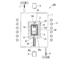
- FIG. 1 It is a cross-sectional schematic diagram which shows an example of a silicon carbide single crystal growth apparatus. It is a cross-sectional schematic diagram of the base periphery of the silicon carbide single crystal growth apparatus shown in FIG.
- FIG. 1 shows an example of a single crystal growth apparatus used in the silicon carbide seed crystal fixing method and silicon carbide single crystal manufacturing method of the present invention.
- the single crystal growth apparatus 100 includes a vacuum vessel 1, and a graphite crucible 6 covered with a heat insulating material 2 is disposed inside the vacuum vessel 1.
- the graphite crucible 6 includes a lid 22 and a main body 21.
- a pedestal 10 that protrudes in a columnar shape is provided on one surface of the lid 22.
- the pedestal 10 protrudes from the lid 22 toward the inner bottom surface 20a.
- Pedestal 10 has one surface (seed crystal side surface) 10a for disposing silicon carbide seed crystal 13 on the inner bottom surface 20a side.
- a silicon carbide seed crystal 13 is bonded to the seed crystal side surface 10 a of the pedestal 10.
- a hollow portion 20 is provided inside the main body portion 21 of the graphite crucible 6.
- a silicon carbide seed crystal 13 is fixed to the upper part of the cavity 20.
- the lower portion in cavity 20 is filled with a sufficient amount of silicon carbide raw material powder 5 for allowing a silicon carbide single crystal to grow on silicon carbide seed crystal 13. That is, cavity portion 20 includes a sufficient amount of silicon carbide raw material 5 at the lower portion and secures a space necessary for crystal growth of the silicon carbide single crystal at the upper portion. Therefore, a silicon carbide single crystal can be grown on the growth surface 13a of the silicon carbide seed crystal 13 toward the inner bottom surface 20a by the sublimation recrystallization method.
- the heat insulating material 2 is installed so as to cover the entire crucible 6 including the lid 22 and the main body 21. At this time, the holes 2c and 2d are formed so that the lower surface and a part of the upper surface of the crucible 6 are exposed.
- the heat insulating material 2 is for maintaining the crucible 6 in a stable high temperature state, and for example, a carbon fiber material can be used. When the crucible 6 can be stably maintained at a high temperature as necessary, the heat insulating material 2 may not be installed.
- the crucible 6 around which the heat insulating material 2 is wound is installed on the support rod 30 so as to be located at the center inside the vacuum vessel 1.
- the support bar 30 has a cylindrical shape, and a hole 30c is provided inside. Both are installed so that the hole 30c provided in the support rod 30 matches the hole 2c provided in the heat insulating material 2. Thereby, the temperature of the lower surface of the crucible 6 can be observed through the hole 30 c of the support rod 30 and the hole 2 c on the lower side of the heat insulating material 2 by the radiation thermometer 9 disposed under the vacuum vessel 1.
- the temperature of the upper surface of the crucible 6 can be observed through another hole 2 d on the upper side of the heat insulating material 2 by another radiation thermometer 9 disposed on the vacuum vessel 1.
- a gas introduction pipe 7 is provided in the upper part of the vacuum vessel 1, and a gas exhaust pipe 8 is provided in the lower part.
- the inside of the vacuum vessel 1 is filled with Ar, for example, and the pressure is adjusted to about 9.3 ⁇ 10 4 Pa.
- a vacuum pump (not shown) connected to the discharge pipe 8
- the air inside the vacuum vessel 1 is exhausted to a reduced pressure state of, for example, 4 ⁇ 10 ⁇ 3 Pa or less.
- a turbo molecular pump can be used as the vacuum pump.
- a high-purity Ar gas is introduced into the vacuum vessel 1 from the introduction tube 7 to make the inside of the vacuum vessel 1 9.3 ⁇ 10 4 Pa in an Ar atmosphere.
- the heating means 3 is arranged outside the vacuum vessel 1.
- the heating means 3 is, for example, a high frequency heating coil.
- the graphite crucible 6 installed at the center in the vacuum vessel 1 can be heated to a temperature of, for example, 1,900 ° C. or more by generating a high frequency by passing a current through the high frequency heating coil. Thereby, silicon carbide raw material powder 5 in graphite crucible 6 is heated, and sublimation gas is generated from silicon carbide raw material powder 5.
- FIG. 2 is a schematic cross-sectional view showing the periphery of the base 10.
- a carbon material such as graphite, dense graphite, glassy carbon, pyrolytic graphite, or the like can be used.
- what coated tantalum carbide on those surfaces can be used.
- silicon carbide can be used as the material of the base 10.
- silicon carbide polycrystal, single crystal, sintered material, or the like can be used.
- WC, ZrC, NbC, TiC, or MoC can be used as the material for the pedestal 10 as the refractory metal carbide. These can also be used as a carbonized metal surface.
- the material for the pedestal is preferably a material that can be easily flattened, and is preferably dense graphite, glassy carbon, pyrolytic graphite, or silicon carbide.
- the pedestal 10 has a function as a pedestal that directly joins the seed crystal
- the lid 22 provided with the pedestal 10 has a function as a lid of the crucible 6.
- the pedestal 10 and the lid 22 may be integrally formed, or may be provided by combining respective members. In either case, it is desirable that the member to which the seed crystal 13 is directly joined is the material of the pedestal. Furthermore, for the function as the pedestal 10, it is desirable to have a thickness that can suppress the influence from the back surface, that is, the lid 22.
- the same material as the pedestal 10 can be used for the lid 22.
- the combination of the material of the lid 22 and the pedestal 10 can be selected from the viewpoint of ease of processing or the like according to the design of the member.
- the carbon material is preferable because it can be easily processed when the lid 22 and the base 10 are mechanically coupled.
- a refractory metal or a metal carbide on the surface thereof is also preferable for the same reason. Since the joint between the base 10 and the lid 22 does not require special adhesion, a mechanical bond or a bond using an adhesive can be used.
- the pedestal 10 may be fixed through the lid 22.
- the temperature of the back surface of the base 10 can be kept lower, and thermal deterioration of the back surface can be suppressed.
- the pedestal 10 can be formed of silicon carbide and the lid 22 can be formed of graphite.
- the thermal conductivity of the base 10 is higher than that of the lid 22.
- silicon carbide seed crystal 13 includes a growth surface 13 a for crystal growth of a silicon carbide single crystal and a bonding surface 13 b bonded to one surface 10 a of pedestal 10.
- silicon carbide seed crystal 13 a single crystal made of silicon carbide (silicon carbide single crystal) is used.
- silicon carbide single crystal a silicon carbide single crystal made by the Atchison method, Rayleigh method, improved Rayleigh method, etc. is cut into a disk shape with a thickness of about 0.3 to 5 mm, and then the cut surface is ground, Use a polished shape.
- a method of performing a final surface treatment with a solution containing HCl after being immersed in a mixed solution containing sulfuric acid (H 2 SO 4 ) or phosphoric acid (H 3 PO 4 ) can be exemplified.
- an inert gas such as argon (Ar).
- the bonding strength between the seed crystal side surface 10a of the pedestal and the seed crystal 13 to be bonded to the surface is affected by oxides, moisture, and the like present in the bonding portion, and is extremely conspicuous in the oxygen concentration in the bonding portions 10a and 13b.
- the adhesive strength becomes weaker as the oxygen atom concentration in the bonding layer is higher.
- the oxygen concentration in the bonding layer can be stably reduced to 1 ⁇ 10 20 atoms / cm 3 or less. If the oxygen atom concentration in the bonding layer on the seed crystal side exceeds 1 ⁇ 10 20 atoms / cm 3 and is present in a large amount, the bonding strength is significantly reduced.
- the surface of the seed crystal subjected to the surface treatment for removing the oxide film or the like is bonded in a high vacuum to the surface of the base from which the oxide film or the like has been removed by the wet treatment method or the dry treatment method.
- the atomic concentration of oxygen in those bonding layers can be further reduced. That is, a bonding layer having strong bonding strength can be formed between the pedestal and the seed crystal.
- bonding is performed in air, a very high cleanliness is required. However, if bonding is performed in a vacuum, such an environment is not necessary and can be manufactured stably at low cost.
- the pedestal and the seed crystal are bonded so that the oxygen concentration is reduced and impurities are not left on the bonding surface, both can be bonded more firmly. Also in this case, it is an effective method to sufficiently perform dry etching.
- the “impurity” means a material other than the material necessary for joining the pedestal and the seed crystal.
- the surface of the pedestal and the seed crystal is smooth, specifically, when the root mean square (rms) value of the surface is 0.3 nm or less, particularly strong bonding can be achieved.
- a smooth surface can be obtained, for example, by chemical mechanical polishing (CMP) means using an abrasive containing colloidal silica when the pedestal and the seed crystal are silicon carbide.
- CMP chemical mechanical polishing
- the polished surface is further treated with an acid solution or ant-kari solution, the surface smoothness can be further improved, and foreign matters and contaminants on the surface in the polishing process can be removed. Thus, a clean surface can be obtained.
- the pedestal and the seed crystal are bonded in a vacuum of 1 ⁇ 10 ⁇ 2 Pascal (Pa) or less, preferably 1 ⁇ 10 ⁇ 3 Pa or less.
- Pa 1 ⁇ 10 ⁇ 2 Pascal
- the energy of the atomic beam or ion beam irradiated when bonding is preferably 50 electron volts (eV) or more.
- “Activation” refers to removing an oxide layer, an impurity layer containing carbon, or the like existing on the surfaces to be bonded, a contaminated layer, and the like, thereby bringing the surfaces into a clean state.
- a strong bond can be formed by directly bonding the bonds of atoms located on the surface. If this irradiation is performed on the surface of at least one of the pedestal and the seed crystal, both can be firmly and reliably bonded. Moreover, if it performs on both surfaces, both can be combined with stronger strength.
- the outermost layer portion having a depth of about 0.5 to 20 ⁇ m has a slightly different lattice constant from the other portions, and even after bonding, a constant thickness is present at the interface.
- Form a layer. This portion is referred to as a bonding layer, and irradiation with an ion beam or the like is also referred to as formation of the bonding layer.
- a beam including an element present in the surface region to be bonded is irradiated, a bond having excellent strength can be formed.
- the surface may be charged when the surface is mainly irradiated with a beam containing ions. If electrical repulsion occurs due to this charging, the base and the seed crystal cannot be firmly joined. For this reason, when irradiating an ion beam and activating a surface, it is preferable that at least one of the joint surfaces of a base and a seed crystal is a material excellent in electroconductivity.
- a beam of an inert gas such as helium (He), neon (Ne), argon (Ar), and krypton (Kr) that does not significantly change the composition or the like is applied.
- the surface can be stably activated.
- an argon (Ar) atomic beam is used, the surface can be easily activated in a short time.
- Helium (He) has a smaller atomic weight than argon (Ar). For this reason, the He beam has a drawback that time is wasted in activating the surfaces to be joined.
- using a krypton (Kr) beam having an atomic weight larger than that of argon is disadvantageous because it may cause impact damage to the surface.
- the surfaces of the pedestal and the seed crystal are made to face each other and overlapped and bonded so that mechanical pressure is applied to the entire bonding surface, so that both can be firmly bonded.
- a pressure in a range of 5 g / cm 2 or more and 200 g / cm 2 or less in a direction perpendicular to the bonding surface (perpendicular).
- the pedestal and the seed crystal can be bonded at a low temperature of 200 ° C. or lower.
- the pedestal and the seed crystal have a surface temperature of 200 ° C. or less, preferably 100 ° C. or less, more preferably room temperature, in which one or both of the surfaces are bonded in the above-mentioned vacuum degree (4 ⁇ 10 ⁇ 3 Pa or less) It can be made to join by applying a pressure in the vertical direction (vertical direction) to the joining surface.
- the pedestal and the seed crystal are bonded to each other after they are heated to a temperature higher than the bonding temperature in a vacuum vessel to release outgas and then cooled to the bonding temperature before contacting. Further, it is also preferable to clean and activate the surface by irradiating accelerated Ar ions or the like at a high temperature before bonding, from the viewpoint of increasing the bonding strength.
- polycrystalline silicon carbide was used as a pedestal, and a silicon carbide seed crystal was bonded thereon.
- Polycrystalline silicon carbide having a diameter of 50 mm (2 inches ⁇ ) and a thickness of 12 mm was used as a pedestal.
- a portion of the pedestal opposite to the portion to which the seed crystal is attached is processed to mechanically attach the pedestal to a graphite lid (crucible lid).
- a 4H (0001) C-plane silicon carbide single crystal wafer having a diameter of 50 mm (2 inches ⁇ ) and a thickness of 0.8 mm was used.
- ⁇ Surface treatment process> First, the surface of the pedestal seed crystal side and the surface of the silicon carbide seed crystal pedestal side were immersed in an aqueous sulfuric acid solution to remove the oxide film on the surface. Next, the seed crystal side surface of the base and the base side surface of the silicon carbide seed crystal were mirror-polished by chemical mechanical polishing (CMP) using an abrasive containing colloidal silica. The root mean square values (rms) after polishing were 0.20 nm and 0.15 nm, respectively.
- CMP chemical mechanical polishing
- the polished lid with the base and the silicon carbide seed crystal were carried into a vacuum apparatus as a pasting apparatus, and the inside of the vacuum apparatus was evacuated to 2 ⁇ 10 ⁇ 5 Pa.
- the surface of the pedestal was irradiated with Ar + ions accelerated to an energy of 800 eV while the lid with the pedestal was heated to a temperature of about 800 ° C. in a vacuum.
- a bonding layer was formed on the surface of the pedestal.
- the surface of the silicon carbide seed crystal was irradiated with Ar + ions accelerated to an energy of 800 eV at a temperature of about 800 ° C.
- a bonding layer was formed on the surface of the silicon carbide seed crystal.
- the temperature of the lid with the base and the silicon carbide seed crystal was lowered to room temperature.
- the graphite crucible lid was placed on the graphite crucible main body to produce a silicon carbide single crystal. While the temperature of the silicon carbide raw material powder is heated to 2,450 ° C., a temperature gradient is provided in the crucible so that the temperature of the silicon carbide seed crystal is lower than the temperature of the silicon carbide raw material powder, and the pressure in the crucible is set to 3 Torr. As a result, crystal growth was performed. Crystal growth was carried out under such normally used conditions. The produced crystal had a thickness of 20 mm, and no through defects generated between the pedestal and the seed crystal were observed, and a high-quality silicon carbide single crystal could be produced.
- dense graphite was used as a pedestal, and a silicon carbide seed crystal was bonded thereon.
- a pedestal integrated lid made of dense graphite having a diameter of 50 mm and having a convex portion having a diameter of 20 mm and a height of 10 mm formed in the center as the pedestal portion was used.
- the silicon carbide seed crystal a 4H (0001) C-plane silicon carbide single crystal wafer having a diameter of 20 mm and a thickness of 0.8 mm was used.
- ⁇ Atom or ion irradiation process> In the same manner as in Example 1, a base-integrated lid and a silicon carbide seed crystal were carried into a vacuum apparatus as a pasting apparatus. Ar + ion irradiation at 800 ° C. before pasting was performed in the same manner, and then a neutral Ar beam neutralized by colliding electrons with both the pedestal and the surface of the silicon carbide seed crystal. Irradiated for 3 minutes.
- the base-integrated lid to which the silicon carbide seed crystal was joined was installed in the graphite crucible main body to produce a silicon carbide single crystal.
- the produced crystal was free from penetration defects generated between the pedestal and the seed crystal, and a high-quality silicon carbide single crystal could be produced.
- a high-quality silicon carbide single crystal having no through defects can be produced.
Landscapes
- Chemical & Material Sciences (AREA)
- Engineering & Computer Science (AREA)
- Crystallography & Structural Chemistry (AREA)
- Materials Engineering (AREA)
- Metallurgy (AREA)
- Organic Chemistry (AREA)
- Inorganic Chemistry (AREA)
- Crystals, And After-Treatments Of Crystals (AREA)
Abstract
貫通欠陥のない高品質の炭化珪素単結晶を製造することができる炭化珪素種結晶の固定方法及び炭化珪素単結晶の製造方法を提供する。 本発明の炭化珪素種結晶の固定方法は、台座上に炭化珪素種結晶を固定する方法であって、前記台座の種結晶側表面を鏡面研磨する工程と、真空中で前記台座の種結晶側表面及び前記炭化珪素種結晶の台座側表面の少なくとも一方に原子またはイオンを照射する照射工程と、真空中で前記台座の種結晶側表面と前記炭化珪素種結晶の台座側表面とを密着させた後に加圧して直接接合する接合工程と、を備えることを特徴とする。
Description
本発明は、炭化珪素種結晶の固定方法及び炭化珪素単結晶の製造方法に関する。
炭化珪素は、熱伝導度が高く、耐熱性及び機械的強度も優れ、放射線にも強いなど、物理的、化学的に安定である。さらに、エネルギーバンドギャップ(禁制帯幅)が広いという特徴を有する。そのため、発光素子、大電力パワーデバイス、耐高温素子、耐放射線素子、高周波素子等への応用が期待されている。
炭化珪素単結晶の製造方法として、台座、例えば黒鉛製の台座上に炭化珪素種結晶を固定し、炭化珪素原料の昇華ガスを供給して炭化珪素種結晶上に炭化珪素の単結晶を成長させる方法が知られている。
台座上に炭化珪素種結晶を固定する方法として、特許文献1には、種結晶の裏面に 0.5~5μmの有機薄膜を被覆してから台座上に装着する方法が開示されている。
また、特許文献2には、種結晶接着面を研磨、RIEなどを行った後、接着剤で接着する方法が開示されている。
特許文献3には、種結晶の裏面を高温安定な物質で被覆してから台座上に装着する方法が開示されている。
特許文献4には、種結晶の貼り付け面に応力緩衝材を挟んで台座上に装着する方法が開示されている。
そして特許文献5には、種結晶を台座上に貼り付けための接着剤が開示されている。
台座上に炭化珪素種結晶を固定する方法として、特許文献1には、種結晶の裏面に 0.5~5μmの有機薄膜を被覆してから台座上に装着する方法が開示されている。
また、特許文献2には、種結晶接着面を研磨、RIEなどを行った後、接着剤で接着する方法が開示されている。
特許文献3には、種結晶の裏面を高温安定な物質で被覆してから台座上に装着する方法が開示されている。
特許文献4には、種結晶の貼り付け面に応力緩衝材を挟んで台座上に装着する方法が開示されている。
そして特許文献5には、種結晶を台座上に貼り付けための接着剤が開示されている。
しかしながら、特許文献1の方法では、有機薄膜を炭化処理して保護膜を得る際に、有機薄膜自身が熱分解してメタンやエチレンといった炭化水素系の分解生成ガスを発生し、この分解生成ガスが保護膜を多孔質にしてガスバリヤ性を低下させ、種結晶の裏面からの昇華を抑制する効果が低下するという問題があった。
また、接着剤を用いて種結晶を台座に貼り付ける方法では、接着剤を乾燥・硬化させる熱処理工程で接着層に気泡が発生し、それが空隙として接着層に残ってしまうことがあった。その結果、空隙がある場所では種結晶から台座へ熱を逃がさないために、局所的に種結晶と台座との間に温度勾配が生じる。すると、種結晶の裏面から温度の低い台座に向かって種結晶の昇華が起こり、これがマイクロパイプと呼ばれる貫通欠陥を発生してしまうという問題があった。
さらにまた、種結晶の貼り付け面に応力緩衝材を挟んで台座上に装着する方法では、緩衝材の熱伝導が充分高くないと、成長した炭化珪素単結晶の台座への放熱が妨げられことになる。すると、単結晶の成長速度を低下すると共に、成長結晶の面内温度分布が不均一になり、単結晶に結晶欠陥を発生させる原因となるという問題があった。
また、接着剤を用いて種結晶を台座に貼り付ける方法では、接着剤を乾燥・硬化させる熱処理工程で接着層に気泡が発生し、それが空隙として接着層に残ってしまうことがあった。その結果、空隙がある場所では種結晶から台座へ熱を逃がさないために、局所的に種結晶と台座との間に温度勾配が生じる。すると、種結晶の裏面から温度の低い台座に向かって種結晶の昇華が起こり、これがマイクロパイプと呼ばれる貫通欠陥を発生してしまうという問題があった。
さらにまた、種結晶の貼り付け面に応力緩衝材を挟んで台座上に装着する方法では、緩衝材の熱伝導が充分高くないと、成長した炭化珪素単結晶の台座への放熱が妨げられことになる。すると、単結晶の成長速度を低下すると共に、成長結晶の面内温度分布が不均一になり、単結晶に結晶欠陥を発生させる原因となるという問題があった。
本発明は、上記事情を鑑みてなされたもので、炭化珪素種結晶と台座との間に膜や接着剤等を介在させずに、炭化珪素種結晶を台座に直接接合することによって、炭化珪素種結晶の裏面(貼り付け面)の温度を均一にして、炭化珪素種結晶の裏面からの部分的昇華を防止し、それによって炭化珪素種結晶に生ずる貫通欠陥の発生を抑制して貫通欠陥のない炭化珪素単結晶の製造を可能にする炭化珪素種結晶の固定方法及びそれを用いる炭化珪素単結晶の製造方法を提供することを目的とする。
本発明は、以下の手段を提供する。
(1)台座上に炭化珪素種結晶を固定する方法であって、前記台座の種結晶側表面を鏡面研磨する工程と、真空中で前記台座の種結晶側表面及び前記炭化珪素種結晶の台座側表面の少なくとも一方に原子またはイオンを照射する照射工程と、真空中で前記台座の種結晶側表面と前記炭化珪素種結晶の台座側表面とを密着させて加圧することにより直接接合する工程と、を備えることを特徴とする炭化珪素単結晶の固定方法。
(2)前記照射工程の前に、前記炭化珪素種結晶の台座側表面を研磨することを特徴とする前項(1)に記載の炭化珪素種結晶の固定方法。
(3)前記台座の種結晶側表面及び/又は前記炭化珪素種結晶の台座側表面を2乗平均平方根値にして0.3nm以下に鏡面研磨することを特徴とする前項(1)又は(2)のいずれかに記載の炭化珪素種結晶の固定方法。
(4)前記照射工程において照射する原子またはイオンは、水素原子(H)、水素分子 (H2)、水素イオン(H+)のいずれか一種であることを特徴とする前項(1)から(3)のいずれか一項に記載の炭化珪素種結晶の固定方法。
(5)前記照射工程において照射する原子またはイオンは、ヘリウム(He)、ネオン(Ne)、アルゴン(Ar)またはクリプトン(Kr)のいずれか一種以上であることを特徴とする前項(1)から(3)のいずれか一項に記載の炭化珪素種結晶の固定方法。
(6)前記照射工程の前に、前記台座の種結晶側表面及び前記炭化珪素種結晶の台座側表面の少なくとも一方に湿式あるいは乾式のエッチング処理を行うことを特徴とする前項(1)から(5)のいずれか一項に記載の炭化珪素種結晶の固定方法。
(7)前記台座の種結晶側表面と前記炭化珪素種結晶の台座側表面とを直接接合する温度が室温以上200℃以下の温度であることを特徴とする前項(1)から(6)のいずれか一項に記載の炭化珪素種結晶の固定方法。
(8)前項(1)から(7)のいずれか一項に記載の炭化珪素種結晶の固定方法を用いて、炭素材料からなる台座上に固定された炭化珪素種結晶に炭化珪素原料の昇華ガスを供給して、前記炭化珪素種結晶上に炭化珪素の単結晶を成長させる炭化珪素単結晶の製造方法。
(1)台座上に炭化珪素種結晶を固定する方法であって、前記台座の種結晶側表面を鏡面研磨する工程と、真空中で前記台座の種結晶側表面及び前記炭化珪素種結晶の台座側表面の少なくとも一方に原子またはイオンを照射する照射工程と、真空中で前記台座の種結晶側表面と前記炭化珪素種結晶の台座側表面とを密着させて加圧することにより直接接合する工程と、を備えることを特徴とする炭化珪素単結晶の固定方法。
(2)前記照射工程の前に、前記炭化珪素種結晶の台座側表面を研磨することを特徴とする前項(1)に記載の炭化珪素種結晶の固定方法。
(3)前記台座の種結晶側表面及び/又は前記炭化珪素種結晶の台座側表面を2乗平均平方根値にして0.3nm以下に鏡面研磨することを特徴とする前項(1)又は(2)のいずれかに記載の炭化珪素種結晶の固定方法。
(4)前記照射工程において照射する原子またはイオンは、水素原子(H)、水素分子 (H2)、水素イオン(H+)のいずれか一種であることを特徴とする前項(1)から(3)のいずれか一項に記載の炭化珪素種結晶の固定方法。
(5)前記照射工程において照射する原子またはイオンは、ヘリウム(He)、ネオン(Ne)、アルゴン(Ar)またはクリプトン(Kr)のいずれか一種以上であることを特徴とする前項(1)から(3)のいずれか一項に記載の炭化珪素種結晶の固定方法。
(6)前記照射工程の前に、前記台座の種結晶側表面及び前記炭化珪素種結晶の台座側表面の少なくとも一方に湿式あるいは乾式のエッチング処理を行うことを特徴とする前項(1)から(5)のいずれか一項に記載の炭化珪素種結晶の固定方法。
(7)前記台座の種結晶側表面と前記炭化珪素種結晶の台座側表面とを直接接合する温度が室温以上200℃以下の温度であることを特徴とする前項(1)から(6)のいずれか一項に記載の炭化珪素種結晶の固定方法。
(8)前項(1)から(7)のいずれか一項に記載の炭化珪素種結晶の固定方法を用いて、炭素材料からなる台座上に固定された炭化珪素種結晶に炭化珪素原料の昇華ガスを供給して、前記炭化珪素種結晶上に炭化珪素の単結晶を成長させる炭化珪素単結晶の製造方法。
本発明の炭化珪素種結晶の固定方法によれば、炭化珪素種結晶の裏面(貼り付け面)の温度を均一にして、炭化珪素種結晶の裏面からの部分的昇華を防止することができる。
さらに、本発明の炭化珪素単結晶の製造方法によれば、貫通欠陥のない高品質の炭化珪素単結晶を製造することができる。
さらに、本発明の炭化珪素単結晶の製造方法によれば、貫通欠陥のない高品質の炭化珪素単結晶を製造することができる。
以下、本発明の一実施形態である炭化珪素種結晶の固定方法及び炭化珪素単結晶の製造方法について、図面を用いて詳細に説明する。なお、以下の説明で用いる図面は、特徴をわかりやすくするために、便宜上特徴となる部分を拡大して示している場合があり、各構成要素の寸法比率などが実際と同じであるとは限らない。
図1に、本発明の炭化珪素種結晶の固定方法及び炭化珪素単結晶の製造方法で用いる単結晶成長装置の一例を示す。
単結晶成長装置100は真空容器1を具備し、その真空容器1の内部に、断熱材2に覆われた黒鉛製るつぼ6が配置されている。黒鉛製るつぼ6は、蓋22と本体部21とから構成されている。
図1に示すように、蓋22の一面には円柱状に突出する台座10が設けられている。本体部21に蓋22をすると、台座10は蓋22から内底面20a側へ向けて突出することとなる。また、台座10は、内底面20a側に炭化珪素種結晶13を配置するための一面(種結晶側表面)10aを有している。この台座10の種結晶側表面10aには炭化珪素種結晶13が接合されている。
単結晶成長装置100は真空容器1を具備し、その真空容器1の内部に、断熱材2に覆われた黒鉛製るつぼ6が配置されている。黒鉛製るつぼ6は、蓋22と本体部21とから構成されている。
図1に示すように、蓋22の一面には円柱状に突出する台座10が設けられている。本体部21に蓋22をすると、台座10は蓋22から内底面20a側へ向けて突出することとなる。また、台座10は、内底面20a側に炭化珪素種結晶13を配置するための一面(種結晶側表面)10aを有している。この台座10の種結晶側表面10aには炭化珪素種結晶13が接合されている。
黒鉛製るつぼ6の本体部21内部には、空洞部20が設けられている。そしてこの空洞部20内の上部には、炭化珪素種結晶13が固定されている。また、空洞部20内の下部には、炭化珪素種結晶13上に炭化珪素単結晶を結晶成長させるのに十分な量の炭化珪素原料粉末5が充填されている。
つまり、空洞部20は、下部に十分な量の炭化珪素原料5を備えるとともに、炭化珪素単結晶を結晶成長させるのに必要な空間を上部に確保している。そのため、昇華再結晶法によって、炭化珪素種結晶13の成長面13aの上に、内底面20a側に向けて炭化珪素単結晶を結晶成長させることができる。
つまり、空洞部20は、下部に十分な量の炭化珪素原料5を備えるとともに、炭化珪素単結晶を結晶成長させるのに必要な空間を上部に確保している。そのため、昇華再結晶法によって、炭化珪素種結晶13の成長面13aの上に、内底面20a側に向けて炭化珪素単結晶を結晶成長させることができる。
上述したように、蓋22と本体部21とを具備するるつぼ6全体を覆うように、断熱材2が設置されている。このとき、るつぼ6の下部表面および上部表面の一部が露出するように孔部2c、2dを形成する。断熱材2は、るつぼ6を安定的に高温状態に維持するためのものであり、例えば、炭素繊維製の材料を用いることができる。るつぼ6を必要な程度に安定的に高温状態に維持することができる場合には、断熱材2は設置しなくてもよい。
断熱材2を巻き付けたるつぼ6は、真空容器1の内部中央に位置するように、支持棒30上に設置されている。支持棒30は筒状であり、内部には孔部30cが設けられている。この支持棒30に設けられた孔部30cを断熱材2に設けた孔部2cと合わせるように、両者を設置する。これにより、真空容器1の下に配置された放射温度計9により、この支持棒30の孔部30cおよび断熱材2の下側の孔部2cを通して、るつぼ6の下部表面の温度を観測できる。同様に、真空容器1の上に配置された別の放射温度計9により、断熱材2の上側の孔部2dを通して、るつぼ6の上部表面の温度を観測できる。
真空容器1の上部にはガス導入管7が設けられ、下部にはガス排気管8が設けられている。真空容器1の内部は、例えば、Ar満たされ、その圧力はで9.3×10⁴Pa程度に調整される。まず、排出管8に接続した真空ポンプ(図示略)を用いて、真空容器1の内部の空気を排気して、たとえば、4×10⁻³Pa以下の減圧状態とする。真空ポンプとしては、例えば、ターボ分子ポンプなどを用いることができる。その後、導入管7から真空容器1の内部に高純度Arガスを導入して、真空容器1の内部をAr雰囲気で9.3×10⁴Paにすればよい。
真空容器1の上部にはガス導入管7が設けられ、下部にはガス排気管8が設けられている。真空容器1の内部は、例えば、Ar満たされ、その圧力はで9.3×10⁴Pa程度に調整される。まず、排出管8に接続した真空ポンプ(図示略)を用いて、真空容器1の内部の空気を排気して、たとえば、4×10⁻³Pa以下の減圧状態とする。真空ポンプとしては、例えば、ターボ分子ポンプなどを用いることができる。その後、導入管7から真空容器1の内部に高純度Arガスを導入して、真空容器1の内部をAr雰囲気で9.3×10⁴Paにすればよい。
真空容器1の外側には、加熱手段3が配置されている。この加熱手段3は、例えば高周波加熱コイルである。高周波加熱コイルに電流を流すことにより高周波を発生させて、真空容器1内の中央に設置された黒鉛製るつぼ6を、例えば、1,900℃以上の温度に加熱することができる。これにより、黒鉛製るつぼ6内の炭化珪素原料粉末5を加熱して、炭化珪素原料粉末5から昇華ガスを発生させる。
図2は、台座10の周辺を示す断面模式図である。
台座10の材料としては、黒鉛、緻密性黒鉛、グラッシーカーボン、パイロリティックグラファイトなどの炭素材料を用いることもできる。また、それらの表面にタンタルカーバイドを被覆したものを用いることができる。さらに、また、台座10の材料としては炭化珪素を用いることができる。炭化珪素は、多結晶、単結晶、焼結材料などを用いることができる。
さらにまた、台座10の材料には、高融点金属炭化物として、WC、ZrC,NbC,TiC,MoCを用いることができる。これらは、金属の表面を炭化させたものとして用いることもできる。
台座の材料は、平坦加工がしやすい物が望ましく、緻密性黒鉛、グラッシーカーボンやパイロリティックグラファイト、炭化珪素が好ましい。
台座10の材料としては、黒鉛、緻密性黒鉛、グラッシーカーボン、パイロリティックグラファイトなどの炭素材料を用いることもできる。また、それらの表面にタンタルカーバイドを被覆したものを用いることができる。さらに、また、台座10の材料としては炭化珪素を用いることができる。炭化珪素は、多結晶、単結晶、焼結材料などを用いることができる。
さらにまた、台座10の材料には、高融点金属炭化物として、WC、ZrC,NbC,TiC,MoCを用いることができる。これらは、金属の表面を炭化させたものとして用いることもできる。
台座の材料は、平坦加工がしやすい物が望ましく、緻密性黒鉛、グラッシーカーボンやパイロリティックグラファイト、炭化珪素が好ましい。
台座10は種結晶と直接接合する台座としての機能を具備し、その台座10が設けられる蓋22はるつぼ6の蓋としての機能を具備する。
台座10および蓋22とは、一体化して形成されていてもよいし、それぞれの部材を結合して設けても良い。なお、どちらの場合であっても、種結晶13が直接接合する部材は、上記台座の材料であることが望ましい。さらに、台座10としての機能のため、裏面から、つまり蓋22からの影響を抑制できる程度の厚さを持つことが望ましい。
台座10および蓋22とは、一体化して形成されていてもよいし、それぞれの部材を結合して設けても良い。なお、どちらの場合であっても、種結晶13が直接接合する部材は、上記台座の材料であることが望ましい。さらに、台座10としての機能のため、裏面から、つまり蓋22からの影響を抑制できる程度の厚さを持つことが望ましい。
蓋22と台座10とを別個の部材とする場合、蓋22は、台座10と同じ材料を用いることができる。蓋22と台座10との材料の組み合わせは、部材の設計に応じて、加工しやすさ等の観点から選択することができる。炭素材料は、蓋22と台座10とを機械的に結合させる場合、加工しやすいことから、好ましい。また、同様に、高融点金属あるいはその表面を金属炭化物としたものも、同様の理由で好ましい。
台座10と蓋22との結合は、特別な密着性を求められるものではないため、機械的な結合や接着剤による結合を用いることができる。また、台座10が蓋22を貫通して固定される構造とすることもできる。この場合、台座10の裏面の温度をより低く保つことができ、裏面の熱劣化を抑制することができる。
また、台座10を炭化珪素で形成し、蓋22を黒鉛で形成することもできる。この場合、台座10の熱伝導率が蓋22に比べて高くなる。これにより、種結晶の温度を周辺部材よりも相対的に下げて、周辺よりも種結晶上への結晶成長を促進する効果が得られる。
台座10と蓋22との結合は、特別な密着性を求められるものではないため、機械的な結合や接着剤による結合を用いることができる。また、台座10が蓋22を貫通して固定される構造とすることもできる。この場合、台座10の裏面の温度をより低く保つことができ、裏面の熱劣化を抑制することができる。
また、台座10を炭化珪素で形成し、蓋22を黒鉛で形成することもできる。この場合、台座10の熱伝導率が蓋22に比べて高くなる。これにより、種結晶の温度を周辺部材よりも相対的に下げて、周辺よりも種結晶上への結晶成長を促進する効果が得られる。
図2に示すように、炭化珪素種結晶13は、炭化珪素単結晶を結晶成長させる成長面13aと、台座10の一面10aに接合される接合面13bとを具備する。
炭化珪素種結晶13としては、炭化珪素からなる単結晶(炭化珪素単結晶)を用いる。
この炭化珪素単結晶としては、アチソン法、レーリー法、改良レーリー法などで作られた炭化珪素単結晶を、厚さ0.3~5mm程度で円板状に切断した後、切断面の研削、研磨を行って形状を整えたものを用いる。なお、炭化珪素種結晶13の最終仕上げとして、この研磨の後に研磨ダメージを取り除くために、犠牲酸化、リアクティブイオンエッチング、化学的機械研磨などを行うことが望ましい。さらに、その後、有機溶剤、酸性溶液またはアルカリ溶液などを用いて、炭化珪素からなる種結晶13の表面を清浄化する。
炭化珪素種結晶13としては、炭化珪素からなる単結晶(炭化珪素単結晶)を用いる。
この炭化珪素単結晶としては、アチソン法、レーリー法、改良レーリー法などで作られた炭化珪素単結晶を、厚さ0.3~5mm程度で円板状に切断した後、切断面の研削、研磨を行って形状を整えたものを用いる。なお、炭化珪素種結晶13の最終仕上げとして、この研磨の後に研磨ダメージを取り除くために、犠牲酸化、リアクティブイオンエッチング、化学的機械研磨などを行うことが望ましい。さらに、その後、有機溶剤、酸性溶液またはアルカリ溶液などを用いて、炭化珪素からなる種結晶13の表面を清浄化する。
以下に、本発明を適用した一実施形態である炭化珪素種結晶の固定方法及び炭化珪素単結晶の製造方法について説明する。
[炭化珪素種結晶の固定方法]
<台座及び/又は種結晶の表面処理工程>
台座10の種結晶側表面10aに、種結晶13を接合するためには、台座10の平坦性、及び清浄性が重要であり、表面処理を行うことが必要である。
例えば、台座を炭化珪素材料で形成する場合、酸化膜を除去するための表面処理手段を必要とする。例えば、アセトンによる洗浄後、塩酸(HCl)、硫酸(H2SO4)、フッ酸(HF)に浸漬する湿式処理法を例示できる。また、硫酸(H2SO4)や燐酸(H3PO4)を含む混合液に浸漬した後、HClを含む溶液で最終的な表面処理を行う手法を例示できる。また、アルゴン(Ar)等の不活性ガスを用いる乾式(ドライ)エッチング法により、表面に在る酸化膜を除去する手段がある。
台座が炭化珪素材料以外の材料で形成されている場合であっても、適宜薬品を選択することにより表面の平坦性、及び清浄性を保つことができる。乾式(ドライ)エッチングは、広範囲の材料に適応することができる。
<台座及び/又は種結晶の表面処理工程>
台座10の種結晶側表面10aに、種結晶13を接合するためには、台座10の平坦性、及び清浄性が重要であり、表面処理を行うことが必要である。
例えば、台座を炭化珪素材料で形成する場合、酸化膜を除去するための表面処理手段を必要とする。例えば、アセトンによる洗浄後、塩酸(HCl)、硫酸(H2SO4)、フッ酸(HF)に浸漬する湿式処理法を例示できる。また、硫酸(H2SO4)や燐酸(H3PO4)を含む混合液に浸漬した後、HClを含む溶液で最終的な表面処理を行う手法を例示できる。また、アルゴン(Ar)等の不活性ガスを用いる乾式(ドライ)エッチング法により、表面に在る酸化膜を除去する手段がある。
台座が炭化珪素材料以外の材料で形成されている場合であっても、適宜薬品を選択することにより表面の平坦性、及び清浄性を保つことができる。乾式(ドライ)エッチングは、広範囲の材料に適応することができる。
また、台座の種結晶側表面10aと、その表面に接合させる種結晶13との接合強度は、接合部に存在する酸化物や水分などに影響され、接合部10aおよび13bにおける酸素濃度に極めて顕著に依存する。接着強度は、その接合層での酸素原子の濃度が高い場合ほど、弱くなる。例えば、上記の通り、台座表面を処理すれば、接合層での酸素濃度を安定的に1×10²⁰原子/cm3以下にすることができる。種結晶側の接合層での酸素原子濃度が1×1020原子/cm3を超えて多量に存在すると接合強度は顕著に低下する。
上記湿式処理法または乾式処理法により、酸化膜等を除去した台座の表面に、同じく酸化膜等を除去するための表面処理を施した種結晶の表面を高真空中で接合させる。これにより、それらの接合層の酸素の原子濃度をさらに低減できる。すなわち、台座と種結晶とで強固な接合強度を有する接合層が形成できる。
また、空気中で接合させる場合には非常に高い清浄度が求められるが、真空中で接合させれば、そのような環境は不要であり、安定して低コストで製造することができる。
また、空気中で接合させる場合には非常に高い清浄度が求められるが、真空中で接合させれば、そのような環境は不要であり、安定して低コストで製造することができる。
酸素濃度を低減させるとともに、接合面に不純物を残存させないように、台座と種結晶とを接合させると、双方をより強固に接合できる。この場合も、乾式(ドライ)エッチングを十分に行うことは有効な方法である。なお、この場合、「不純物」とは、台座と種結晶とを接合させるのに必要な材料以外の材料を意味する。
また、台座及び種結晶の表面が平滑である場合、具体的には表面の2乗平均平方根(rms)値が、0.3nm以下である場合、特に強度な接合とすることができる。
このような平滑な表面は、例えば、台座及び種結晶が炭化珪素の場合、コロイダルシリカを含む研磨剤を用いる化学的機械研磨(CMP)手段により得ることができる。化学的機械研磨を行った後、研磨した表面をさらに、酸溶液あるいはアリカリ溶液で処理すれば、より一層表面の平滑度を向上させられると共に、研磨工程での表面への異物や汚染物を除去して、清浄な表面を得ることができる。
このような平滑な表面は、例えば、台座及び種結晶が炭化珪素の場合、コロイダルシリカを含む研磨剤を用いる化学的機械研磨(CMP)手段により得ることができる。化学的機械研磨を行った後、研磨した表面をさらに、酸溶液あるいはアリカリ溶液で処理すれば、より一層表面の平滑度を向上させられると共に、研磨工程での表面への異物や汚染物を除去して、清浄な表面を得ることができる。
台座及び種結晶は、圧力にして1×10⁻²パスカル(Pa)以下、好ましくは、1×10⁻³ Pa以下の真空中で接合させる。特に、上記のように、研磨された平滑な表面を相互に接合させると強固に接合できる。
双方を接合させるに際し、原子のビームまたはイオンビームを接合させようとする表面の各々に照射し、接合させる表面を活性化させることが重要である。接合させる際に照射する原子のビームまたはイオンビームのエネルギーは50エレクトロンボルト(eV)以上を有することが好ましい。「活性化」とは、接合させる表面に存在する酸化膜、炭素等を含む不純物層や汚染層などを除去し、表面を清浄な状態にすることをいう。
表面層を除去することにより、表面に位置する原子の結合手を直接結合させることにより強固な接合を形成することができる。この照射を、台座及び種結晶の少なくとも一方の表面に行えば、双方を強固に確実に接合させられる。また、双方の表面に行うと、より強固な強度で双方を結合させることができる。
活性化された表面は、深さ0.5~20μm程度の最表層部分が、他の部分とは格子定数がわずかに異なる状態となり、接合を行った後にも、その界面に一定の厚さの層を形成する。この部分を接合層と称し、イオンビーム等を照射することを接合層の形成とも言うこととする。
双方を接合させるに際し、原子のビームまたはイオンビームを接合させようとする表面の各々に照射し、接合させる表面を活性化させることが重要である。接合させる際に照射する原子のビームまたはイオンビームのエネルギーは50エレクトロンボルト(eV)以上を有することが好ましい。「活性化」とは、接合させる表面に存在する酸化膜、炭素等を含む不純物層や汚染層などを除去し、表面を清浄な状態にすることをいう。
表面層を除去することにより、表面に位置する原子の結合手を直接結合させることにより強固な接合を形成することができる。この照射を、台座及び種結晶の少なくとも一方の表面に行えば、双方を強固に確実に接合させられる。また、双方の表面に行うと、より強固な強度で双方を結合させることができる。
活性化された表面は、深さ0.5~20μm程度の最表層部分が、他の部分とは格子定数がわずかに異なる状態となり、接合を行った後にも、その界面に一定の厚さの層を形成する。この部分を接合層と称し、イオンビーム等を照射することを接合層の形成とも言うこととする。
<原子またはイオン照射工程>
台座と種結晶とを強固に接合させることができる照射種として、水素原子(H)、水素分子(H2)、または水素イオン(H+)ビームを例示できる。また、接合させようとする表面領域に存在する元素を含むビームを照射すると、強度に優れる接合を形成できる。台座及び種結晶の表面の電気抵抗が高い場合、主にイオンを含むビームを表面に照射すると、表面が帯電することがある。この帯電により電気的な反発が起こると、台座と種結晶とを強固に接合できない。このため、イオンビームを照射して表面を活性化する場合、台座と種結晶との接合面の少なくとも一方が、導電性に優れる材料であることが好ましい。
台座と種結晶とを強固に接合させることができる照射種として、水素原子(H)、水素分子(H2)、または水素イオン(H+)ビームを例示できる。また、接合させようとする表面領域に存在する元素を含むビームを照射すると、強度に優れる接合を形成できる。台座及び種結晶の表面の電気抵抗が高い場合、主にイオンを含むビームを表面に照射すると、表面が帯電することがある。この帯電により電気的な反発が起こると、台座と種結晶とを強固に接合できない。このため、イオンビームを照射して表面を活性化する場合、台座と種結晶との接合面の少なくとも一方が、導電性に優れる材料であることが好ましい。
また、台座及び種結晶の表面領域において、それらの組成等に顕著な変化を及ぼさないヘリウム(He)、ネオン(Ne)、アルゴン(Ar)、及びクリプトン(Kr)等の不活性ガスのビームを用いると、安定して表面を活性化させることができる。特に、アルゴン(Ar)原子ビームを用いると、表面を短時間に簡便に活性化できる。ヘリウム(He)は、アルゴン(Ar)よりも原子量が小さい。このため、Heビームでは接合させようとする表面の活性化に時間が浪費される欠点がある。一方、アルゴンよりは原子量が大きいクリプトン(Kr)のビームを用いると、表面に衝撃損傷を与えかねず不都合である。
<接合工程>
台座と種結晶との表面を対向させ、接合面全般に機械的圧力が及ぶように重ね合わせて接合させると、双方を強固に接合させることができ、好ましい。具体的には、接合面に対して垂直方向に(鉛直に)、5g/cm2以上で200g/cm2以下の範囲の圧力を加えることが好ましい。この手法によれば、台座及び種結晶、あるいはその双方が例えば、反っていても、その反りを解消して、均一な強度で接合することができる。
台座と種結晶との表面を対向させ、接合面全般に機械的圧力が及ぶように重ね合わせて接合させると、双方を強固に接合させることができ、好ましい。具体的には、接合面に対して垂直方向に(鉛直に)、5g/cm2以上で200g/cm2以下の範囲の圧力を加えることが好ましい。この手法によれば、台座及び種結晶、あるいはその双方が例えば、反っていても、その反りを解消して、均一な強度で接合することができる。
上記の通り、高真空中で、原子あるいはイオンビームを使用して、活性化させた面を接合させる場合、台座及び種結晶の接合を、200℃以下の低温で実施することができる。
台座及び種結晶は、上記の望ましい真空度(4×10⁻³Pa以下)の真空中において、一方又は双方の接合させる表面の温度を、200℃以下、好ましくは100℃以下、さらに好ましくは室温に調整し、接合面に対して垂直方向(鉛直方向)の圧力を加えることにより、接合させることができる。200℃を超える高温環境下で接合させると、台座を構成する材料からアウトガスが発生し、表面の清浄に影響を与え、その結果接合強度が弱くなることがある。
本接合方法では、イオンビーム照射により結合手を持った原子が露出しているため、表面は結合力の大きい活性化した状態と考えられる。このため、常温でも強固な結合を得ることができる。つまり、結晶やその界面の熱的な変性を避ける点からも、不必要な高温で接合を行わない方が望ましい。
台座及び種結晶は、上記の望ましい真空度(4×10⁻³Pa以下)の真空中において、一方又は双方の接合させる表面の温度を、200℃以下、好ましくは100℃以下、さらに好ましくは室温に調整し、接合面に対して垂直方向(鉛直方向)の圧力を加えることにより、接合させることができる。200℃を超える高温環境下で接合させると、台座を構成する材料からアウトガスが発生し、表面の清浄に影響を与え、その結果接合強度が弱くなることがある。
本接合方法では、イオンビーム照射により結合手を持った原子が露出しているため、表面は結合力の大きい活性化した状態と考えられる。このため、常温でも強固な結合を得ることができる。つまり、結晶やその界面の熱的な変性を避ける点からも、不必要な高温で接合を行わない方が望ましい。
さらに、台座及び種結晶は、接触させる前に、真空容器中で、接合温度よりも高い温度に昇温して、アウトガスを放出させ、その後、接合させる温度まで冷却した後に接合させることが好ましい。さらに、接合前に、高温で、加速されたArイオンなどを照射して表面を清浄化、活性化することも、接合強度を高める点で好ましい。
[炭化珪素単結晶の製造方法]
以上の手順で台座上に炭化珪素種結晶を接合させた蓋をるつぼの本体部上に装着する。
その後は、通常の炭化珪素単結晶の製造方法を用いて炭化珪素単結晶を製造することができる。
以上の手順で台座上に炭化珪素種結晶を接合させた蓋をるつぼの本体部上に装着する。
その後は、通常の炭化珪素単結晶の製造方法を用いて炭化珪素単結晶を製造することができる。
本実施例では、台座として多結晶炭化珪素を用いて、その上に炭化珪素種結晶を接合させた。
直径50mm(2インチφ)、厚さ12mmの多結晶炭化珪素を台座として用いた。後述するように、接合工程後に、この台座の、種結晶を取り付ける部分とは逆側の部分を加工し、機械的に黒鉛製の蓋(るつぼ蓋)に台座を取り付ける構造とする。
炭化珪素種結晶としては、直径50mm(2インチφ)、厚さ0.8mmの4H(0001)C面の炭化珪素単結晶ウェーハを用いた。
直径50mm(2インチφ)、厚さ12mmの多結晶炭化珪素を台座として用いた。後述するように、接合工程後に、この台座の、種結晶を取り付ける部分とは逆側の部分を加工し、機械的に黒鉛製の蓋(るつぼ蓋)に台座を取り付ける構造とする。
炭化珪素種結晶としては、直径50mm(2インチφ)、厚さ0.8mmの4H(0001)C面の炭化珪素単結晶ウェーハを用いた。
<表面処理工程>
まず、台座の種結晶側表面及び炭化珪素種結晶の台座側表面を、硫酸水溶液に浸漬して表面の酸化膜を除去した。
次に、台座の種結晶側表面及び炭化珪素種結晶の台座側表面を、コロイダルシリカを含む研磨剤を用いて化学的機械研磨(CMP)によって鏡面研磨した。研磨後の2乗平均平方根値(rms)はそれぞれ、0.20nm、0.15nmだった。
まず、台座の種結晶側表面及び炭化珪素種結晶の台座側表面を、硫酸水溶液に浸漬して表面の酸化膜を除去した。
次に、台座の種結晶側表面及び炭化珪素種結晶の台座側表面を、コロイダルシリカを含む研磨剤を用いて化学的機械研磨(CMP)によって鏡面研磨した。研磨後の2乗平均平方根値(rms)はそれぞれ、0.20nm、0.15nmだった。
<原子またはイオン照射工程>
次に、貼り付け装置である真空装置内に、研磨後の台座付き蓋及び炭化珪素種結晶を搬入し、2×10⁻⁵Paまで真空装置内を真空に排気した。その後まず、台座付き蓋を真空中で約800℃の温度に加熱しつつ、800eVのエネルギーに加速されたAr+イオンを、台座の表面に照射した。これにより、台座の表面に接合層を形成した。
同様に、約800℃の温度で800eVのエネルギーに加速されたAr+イオンを炭化珪素種結晶の表面に照射した。これにより、炭化珪素種結晶の表面に接合層を形成した。その後、台座付き蓋及び炭化珪素種結晶の温度を室温までさげた。
次に、貼り付け装置である真空装置内に、研磨後の台座付き蓋及び炭化珪素種結晶を搬入し、2×10⁻⁵Paまで真空装置内を真空に排気した。その後まず、台座付き蓋を真空中で約800℃の温度に加熱しつつ、800eVのエネルギーに加速されたAr+イオンを、台座の表面に照射した。これにより、台座の表面に接合層を形成した。
同様に、約800℃の温度で800eVのエネルギーに加速されたAr+イオンを炭化珪素種結晶の表面に照射した。これにより、炭化珪素種結晶の表面に接合層を形成した。その後、台座付き蓋及び炭化珪素種結晶の温度を室温までさげた。
次に、台座及び炭化珪素種結晶の双方の表面に、電子を衝突させて中性(ニュートラル)化した中性のArビームを3分間照射した。
<接合工程>
その後、真空に維持した真空装置内で、台座及び炭化珪素種結晶の双方の表面を重ね合わせ、各々の表面での圧力が20g/cm2となるように荷重をかけ、室温で接合した。
その後、真空に維持した真空装置内で、台座及び炭化珪素種結晶の双方の表面を重ね合わせ、各々の表面での圧力が20g/cm2となるように荷重をかけ、室温で接合した。
<るつぼ蓋の作製>
こうして炭化珪素種結晶を接合した台座を黒鉛製るつぼの蓋となる黒鉛製部材に機械的に取り付けて、黒鉛製るつぼ蓋を作製した。
こうして炭化珪素種結晶を接合した台座を黒鉛製るつぼの蓋となる黒鉛製部材に機械的に取り付けて、黒鉛製るつぼ蓋を作製した。
<炭化珪素単結晶の製造>
この黒鉛製るつぼ蓋を黒鉛製るつぼ本体部に設置して、炭化珪素単結晶の製造を行った。
炭化珪素原料粉末の温度を2,450℃に加熱するとともに、炭化珪素種結晶の温度が炭化珪素原料粉末の温度よりも低くなるように、るつぼ内に温度勾配を設け、るつぼ内の圧力を3Torrとして、結晶成長を行った。このような通常用いられる条件で結晶成長を行った。
作製された結晶は厚さ20mmで、台座と種結晶との間から発生する貫通欠陥は見られず高品質の炭化珪素単結晶が製造できた。
この黒鉛製るつぼ蓋を黒鉛製るつぼ本体部に設置して、炭化珪素単結晶の製造を行った。
炭化珪素原料粉末の温度を2,450℃に加熱するとともに、炭化珪素種結晶の温度が炭化珪素原料粉末の温度よりも低くなるように、るつぼ内に温度勾配を設け、るつぼ内の圧力を3Torrとして、結晶成長を行った。このような通常用いられる条件で結晶成長を行った。
作製された結晶は厚さ20mmで、台座と種結晶との間から発生する貫通欠陥は見られず高品質の炭化珪素単結晶が製造できた。
本実施例では、台座として緻密性黒鉛を用いて、その上に炭化珪素種結晶を接合させた。
本実施例では、台座部として直径20mmで高さ10mmの凸部を中央に形成した、直径50mmの緻密性黒鉛製の台座一体型の蓋を用いた。
炭化珪素種結晶としては直径20mm、厚さ0.8mmの4H (0001)C面の炭化珪素単結晶ウェーハを用いた。
本実施例では、台座部として直径20mmで高さ10mmの凸部を中央に形成した、直径50mmの緻密性黒鉛製の台座一体型の蓋を用いた。
炭化珪素種結晶としては直径20mm、厚さ0.8mmの4H (0001)C面の炭化珪素単結晶ウェーハを用いた。
<表面処理工程>
まず、台座の種結晶を接合させる面を鏡面研磨加工により平坦化した。その後、真空及び不活性ガス中ベーキングにより、表面及び内部の不純物除去を行った。
まず、台座の種結晶を接合させる面を鏡面研磨加工により平坦化した。その後、真空及び不活性ガス中ベーキングにより、表面及び内部の不純物除去を行った。
<原子またはイオン照射工程>
実施例1と同様に、貼り付け装置である真空装置内に、台座一体型の蓋及び炭化珪素種結晶を搬入した。貼り付け前の800℃でのAr+イオン照射も同様に行い、次に、台座及び炭化珪素種結晶の双方の表面に、電子を衝突させて中性(ニュートラル)化した中性のArビームを3分間照射した。
実施例1と同様に、貼り付け装置である真空装置内に、台座一体型の蓋及び炭化珪素種結晶を搬入した。貼り付け前の800℃でのAr+イオン照射も同様に行い、次に、台座及び炭化珪素種結晶の双方の表面に、電子を衝突させて中性(ニュートラル)化した中性のArビームを3分間照射した。
<接合工程>
その後、真空に維持した真空装置内で、台座部及び炭化珪素種結晶の双方の表面を重ね合わせ、各々の表面での圧力が50g/cm2となるように荷重をかけ、室温で接合した。
その後、真空に維持した真空装置内で、台座部及び炭化珪素種結晶の双方の表面を重ね合わせ、各々の表面での圧力が50g/cm2となるように荷重をかけ、室温で接合した。
<炭化珪素単結晶の製造>
こうして炭化珪素種結晶を接合した台座一体型の蓋を、黒鉛製るつぼ本体部に設置して、炭化珪素単結晶の製造を行った。
作製された結晶は、台座と種結晶との間から発生する貫通欠陥は見られず高品質の炭化珪素単結晶が製造できた。
こうして炭化珪素種結晶を接合した台座一体型の蓋を、黒鉛製るつぼ本体部に設置して、炭化珪素単結晶の製造を行った。
作製された結晶は、台座と種結晶との間から発生する貫通欠陥は見られず高品質の炭化珪素単結晶が製造できた。
本発明の炭化珪素種結晶の固定方法及び炭化珪素単結晶の製造方法によれば、貫通欠陥のない高品質の炭化珪素単結晶を製造できる。
1 真空容器
3 加熱手段
5 炭化珪素原料粉末
6 黒鉛製るつぼ
10 台座
10a 種結晶側表面
13 炭化珪素種結晶
13b 接合面
21 本体部
22 蓋
100 単結晶成長装置
3 加熱手段
5 炭化珪素原料粉末
6 黒鉛製るつぼ
10 台座
10a 種結晶側表面
13 炭化珪素種結晶
13b 接合面
21 本体部
22 蓋
100 単結晶成長装置
Claims (8)
- 台座上に炭化珪素種結晶を固定する方法であって、
前記台座の種結晶側表面を鏡面研磨する工程と、
真空中で前記台座の種結晶側表面及び前記炭化珪素種結晶の台座側表面の少なくとも一方に原子またはイオンを照射する照射工程と、
真空中で前記台座の種結晶側表面と前記炭化珪素種結晶の台座側表面とを密着させて加圧することにより直接接合する工程と、
を備えることを特徴とする炭化珪素種結晶の固定方法。 - 前記照射工程の前に、前記炭化珪素種結晶の台座側表面を研磨することを特徴とする請求項1に記載の炭化珪素種結晶の固定方法。
- 前記台座の種結晶側表面及び/又は前記炭化珪素種結晶の台座側表面を、2乗平均平方根値にして、0.3nm以下に鏡面研磨することを特徴とする請求項1に記載の炭化珪素種結晶の固定方法。
- 前記照射工程において照射する原子またはイオンは、水素原子(H)、水素分子(H2)、水素イオン(H+)のいずれか一種であることを特徴とする請求項1に記載の炭化珪素種結晶の固定方法。
- 前記照射工程において照射する原子またはイオンは、ヘリウム(He)、ネオン(Ne)、アルゴン(Ar)またはクリプトン(Kr)のいずれか一種以上であることを特徴とする請求項1に記載の炭化珪素種結晶の固定方法。
- 前記照射工程の前に、前記台座の種結晶側表面及び前記炭化珪素種結晶の台座側表面の少なくとも一方に、湿式エッチング処理または乾式エッチング処理を行うことを特徴とする請求項1に記載の炭化珪素種結晶の固定方法。
- 前記台座の種結晶側表面と前記炭化珪素種結晶の台座側表面とを直接接合する温度が室温以上200℃以下の温度であることを特徴とする、請求項1に記載の炭化珪素種結晶の固定方法。
- 請求項1に記載の炭化珪素種結晶の固定方法を用いて、炭素材料からなる台座上に固定された炭化珪素種結晶に炭化珪素原料の昇華ガスを供給して、前記炭化珪素種結晶上に炭化珪素の単結晶を成長させる炭化珪素単結晶の製造方法。
Priority Applications (1)
| Application Number | Priority Date | Filing Date | Title |
|---|---|---|---|
| US13/582,592 US20130000547A1 (en) | 2010-03-05 | 2011-03-02 | Method for fixing silicon carbide seed crystal and method for producing single crystal silicon carbide |
Applications Claiming Priority (2)
| Application Number | Priority Date | Filing Date | Title |
|---|---|---|---|
| JP2010-049627 | 2010-03-05 | ||
| JP2010049627A JP5624777B2 (ja) | 2010-03-05 | 2010-03-05 | 炭化珪素種結晶の固定方法及び炭化珪素単結晶の製造方法 |
Publications (1)
| Publication Number | Publication Date |
|---|---|
| WO2011108587A1 true WO2011108587A1 (ja) | 2011-09-09 |
Family
ID=44542234
Family Applications (1)
| Application Number | Title | Priority Date | Filing Date |
|---|---|---|---|
| PCT/JP2011/054766 Ceased WO2011108587A1 (ja) | 2010-03-05 | 2011-03-02 | 炭化珪素種結晶の固定方法及び炭化珪素単結晶の製造方法 |
Country Status (3)
| Country | Link |
|---|---|
| US (1) | US20130000547A1 (ja) |
| JP (1) | JP5624777B2 (ja) |
| WO (1) | WO2011108587A1 (ja) |
Families Citing this family (13)
| Publication number | Priority date | Publication date | Assignee | Title |
|---|---|---|---|---|
| JP5689661B2 (ja) * | 2010-11-30 | 2015-03-25 | 株式会社フジクラ | 種結晶保持体及びこれを用いた単結晶の製造方法 |
| JP5946065B2 (ja) * | 2013-02-19 | 2016-07-05 | 三菱重工工作機械株式会社 | 常温接合装置および常温接合方法 |
| JP6387375B2 (ja) | 2016-07-19 | 2018-09-05 | 株式会社サイコックス | 半導体基板 |
| US10793972B1 (en) | 2017-07-11 | 2020-10-06 | Ii-Vi Delaware, Inc. | High quality silicon carbide crystals and method of making the same |
| JP7232495B2 (ja) * | 2018-03-08 | 2023-03-03 | ランテクニカルサービス株式会社 | SiCインゴット製造用基板の製造方法、及び、SiCインゴット製造用基板 |
| JP7068914B2 (ja) * | 2018-04-26 | 2022-05-17 | 昭和電工株式会社 | 断熱性遮蔽部材及びそれを備えた単結晶製造装置 |
| CN110129886A (zh) * | 2019-06-26 | 2019-08-16 | 哈尔滨科友半导体产业装备与技术研究院有限公司 | 一种碳化硅单晶生长中的籽晶固定装置 |
| CN115341285A (zh) * | 2022-08-10 | 2022-11-15 | 北京清研半导科技有限公司 | 一种碳化硅籽晶真空粘接的设备及方法 |
| EP4324961A1 (en) * | 2022-08-17 | 2024-02-21 | SiCrystal GmbH | Method for producing a bulk sic single crystal with improved quality using a sic seed crystal with a temporary protective oxide layer, and sic seed crystal with protective oxide layer |
| CN115261992A (zh) * | 2022-09-28 | 2022-11-01 | 青禾晶元(天津)半导体材料有限公司 | 一种碳化硅复合籽晶及其制备方法与应用 |
| JP7381031B1 (ja) * | 2023-03-29 | 2023-11-15 | 有限会社サクセス | SiC延長インゴットの製造方法 |
| CN120712385A (zh) * | 2023-02-24 | 2025-09-26 | 萨克瑟斯有限公司 | 半导体结晶的研磨加工方法及使用该研磨加工方法的SiC延长锭的制造方法 |
| CN118516767B (zh) * | 2024-06-18 | 2025-01-24 | 江苏芯恒惟业电子科技有限公司 | 一种碳化硅籽晶粘贴设备 |
Citations (4)
| Publication number | Priority date | Publication date | Assignee | Title |
|---|---|---|---|---|
| JPH0796378A (ja) * | 1993-09-29 | 1995-04-11 | Natl Res Inst For Metals | 接合方法 |
| JP2002308697A (ja) * | 2001-04-05 | 2002-10-23 | Nippon Steel Corp | 炭化珪素単結晶インゴット及びその製造方法並びに炭化珪素単結晶育成用種結晶の装着方法 |
| JP2003119098A (ja) * | 2001-10-16 | 2003-04-23 | Denso Corp | 種結晶の固定方法および固定状態の評価方法 |
| JP2005104810A (ja) * | 2003-10-02 | 2005-04-21 | Hitachi Metals Ltd | 異種材料複合体およびその製造方法 |
-
2010
- 2010-03-05 JP JP2010049627A patent/JP5624777B2/ja active Active
-
2011
- 2011-03-02 WO PCT/JP2011/054766 patent/WO2011108587A1/ja not_active Ceased
- 2011-03-02 US US13/582,592 patent/US20130000547A1/en not_active Abandoned
Patent Citations (4)
| Publication number | Priority date | Publication date | Assignee | Title |
|---|---|---|---|---|
| JPH0796378A (ja) * | 1993-09-29 | 1995-04-11 | Natl Res Inst For Metals | 接合方法 |
| JP2002308697A (ja) * | 2001-04-05 | 2002-10-23 | Nippon Steel Corp | 炭化珪素単結晶インゴット及びその製造方法並びに炭化珪素単結晶育成用種結晶の装着方法 |
| JP2003119098A (ja) * | 2001-10-16 | 2003-04-23 | Denso Corp | 種結晶の固定方法および固定状態の評価方法 |
| JP2005104810A (ja) * | 2003-10-02 | 2005-04-21 | Hitachi Metals Ltd | 異種材料複合体およびその製造方法 |
Non-Patent Citations (1)
| Title |
|---|
| YASUHIKO SASAKI ET AL.: "Development of Surface Activated Bonding Equipment for Wafers", 4TH SYMPOSIUM ON MICROJOINING AND ASSEMBLY TECHNOLOGY IN ELECTRONICS RONBUNSHU, 1998, pages 167 - 172 * |
Also Published As
| Publication number | Publication date |
|---|---|
| US20130000547A1 (en) | 2013-01-03 |
| JP2011184224A (ja) | 2011-09-22 |
| JP5624777B2 (ja) | 2014-11-12 |
Similar Documents
| Publication | Publication Date | Title |
|---|---|---|
| JP5624777B2 (ja) | 炭化珪素種結晶の固定方法及び炭化珪素単結晶の製造方法 | |
| JP5896038B2 (ja) | ナノカーボン膜の作製方法 | |
| KR101267135B1 (ko) | 탄화규소 단결정 성장용 종결정 및 그 제조 방법 및 탄화규소 단결정 및 그 제조 방법 | |
| US7833878B2 (en) | Method for manufacturing SOI substrate | |
| JP7115297B2 (ja) | 多結晶ダイヤモンド自立基板及びその製造方法 | |
| EP2955167A1 (en) | Silicon carbide-tantalum carbide composite and susceptor | |
| JP7542053B2 (ja) | 多結晶炭化ケイ素で作られたキャリア基板上に単結晶炭化ケイ素の薄層を含む複合構造を製造するためのプロセス | |
| JP2008198656A (ja) | 半導体基板の製造方法 | |
| KR101553387B1 (ko) | 단결정 탄화 규소의 성장 방법 | |
| EP2879176A1 (en) | Method for producing hybrid substrates, and hybrid substrate | |
| JP2011020860A (ja) | 炭化珪素単結晶製造用坩堝及び炭化珪素単結晶の製造方法 | |
| JP2010064918A (ja) | 炭化珪素単結晶の製造方法、炭化珪素単結晶ウェーハ及び炭化珪素単結晶半導体パワーデバイス | |
| TW202139261A (zh) | 包含單晶SiC所製成之薄層在SiC所製成之載體基板上之複合結構的製造方法 | |
| CN114730699B (zh) | 制造包括位于由SiC制成的载体基板上的单晶SiC薄层的复合结构的方法 | |
| JP2008021992A (ja) | 接合界面安定化のための熱処理 | |
| TWI450366B (zh) | Semiconductor substrate manufacturing method | |
| CN116084011A (zh) | 一种碳化硅复合衬底及其制造方法 | |
| CN115261992A (zh) | 一种碳化硅复合籽晶及其制备方法与应用 | |
| TW202331791A (zh) | 用於製作在多晶碳化矽載體底材上包括單晶碳化矽薄層之複合結構之方法 | |
| JP5830255B2 (ja) | 半導体基板の製造方法 | |
| JP4457708B2 (ja) | 種結晶固定方法並びに単結晶の製造方法 | |
| JP2015030659A (ja) | 単結晶の製造方法 | |
| TW202205357A (zh) | 用於製作複合結構之方法,該複合結構包含一單晶sic薄層在一sic載體底材上 |
Legal Events
| Date | Code | Title | Description |
|---|---|---|---|
| 121 | Ep: the epo has been informed by wipo that ep was designated in this application |
Ref document number: 11750696 Country of ref document: EP Kind code of ref document: A1 |
|
| WWE | Wipo information: entry into national phase |
Ref document number: 13582592 Country of ref document: US |
|
| NENP | Non-entry into the national phase |
Ref country code: DE |
|
| 122 | Ep: pct application non-entry in european phase |
Ref document number: 11750696 Country of ref document: EP Kind code of ref document: A1 |