WO2011102140A1 - 半導体装置の製造方法 - Google Patents
半導体装置の製造方法 Download PDFInfo
- Publication number
- WO2011102140A1 WO2011102140A1 PCT/JP2011/000901 JP2011000901W WO2011102140A1 WO 2011102140 A1 WO2011102140 A1 WO 2011102140A1 JP 2011000901 W JP2011000901 W JP 2011000901W WO 2011102140 A1 WO2011102140 A1 WO 2011102140A1
- Authority
- WO
- WIPO (PCT)
- Prior art keywords
- pattern
- film
- forming
- semiconductor device
- manufacturing
- Prior art date
- Legal status (The legal status is an assumption and is not a legal conclusion. Google has not performed a legal analysis and makes no representation as to the accuracy of the status listed.)
- Ceased
Links
Images








Classifications
-
- H—ELECTRICITY
- H10—SEMICONDUCTOR DEVICES; ELECTRIC SOLID-STATE DEVICES NOT OTHERWISE PROVIDED FOR
- H10P—GENERIC PROCESSES OR APPARATUS FOR THE MANUFACTURE OR TREATMENT OF DEVICES COVERED BY CLASS H10
- H10P76/00—Manufacture or treatment of masks on semiconductor bodies, e.g. by lithography or photolithography
- H10P76/20—Manufacture or treatment of masks on semiconductor bodies, e.g. by lithography or photolithography of masks comprising organic materials
- H10P76/204—Manufacture or treatment of masks on semiconductor bodies, e.g. by lithography or photolithography of masks comprising organic materials of organic photoresist masks
- H10P76/2041—Photolithographic processes
-
- H—ELECTRICITY
- H10—SEMICONDUCTOR DEVICES; ELECTRIC SOLID-STATE DEVICES NOT OTHERWISE PROVIDED FOR
- H10P—GENERIC PROCESSES OR APPARATUS FOR THE MANUFACTURE OR TREATMENT OF DEVICES COVERED BY CLASS H10
- H10P50/00—Etching of wafers, substrates or parts of devices
- H10P50/71—Etching of wafers, substrates or parts of devices using masks for conductive or resistive materials
-
- H—ELECTRICITY
- H10—SEMICONDUCTOR DEVICES; ELECTRIC SOLID-STATE DEVICES NOT OTHERWISE PROVIDED FOR
- H10B—ELECTRONIC MEMORY DEVICES
- H10B10/00—Static random access memory [SRAM] devices
-
- H—ELECTRICITY
- H10—SEMICONDUCTOR DEVICES; ELECTRIC SOLID-STATE DEVICES NOT OTHERWISE PROVIDED FOR
- H10B—ELECTRONIC MEMORY DEVICES
- H10B10/00—Static random access memory [SRAM] devices
- H10B10/12—Static random access memory [SRAM] devices comprising a MOSFET load element
-
- H—ELECTRICITY
- H10—SEMICONDUCTOR DEVICES; ELECTRIC SOLID-STATE DEVICES NOT OTHERWISE PROVIDED FOR
- H10D—INORGANIC ELECTRIC SEMICONDUCTOR DEVICES
- H10D89/00—Aspects of integrated devices not covered by groups H10D84/00 - H10D88/00
- H10D89/10—Integrated device layouts
-
- H—ELECTRICITY
- H10—SEMICONDUCTOR DEVICES; ELECTRIC SOLID-STATE DEVICES NOT OTHERWISE PROVIDED FOR
- H10P—GENERIC PROCESSES OR APPARATUS FOR THE MANUFACTURE OR TREATMENT OF DEVICES COVERED BY CLASS H10
- H10P76/00—Manufacture or treatment of masks on semiconductor bodies, e.g. by lithography or photolithography
- H10P76/40—Manufacture or treatment of masks on semiconductor bodies, e.g. by lithography or photolithography of masks comprising inorganic materials
- H10P76/408—Manufacture or treatment of masks on semiconductor bodies, e.g. by lithography or photolithography of masks comprising inorganic materials characterised by their sizes, orientations, dispositions, behaviours or shapes
- H10P76/4085—Manufacture or treatment of masks on semiconductor bodies, e.g. by lithography or photolithography of masks comprising inorganic materials characterised by their sizes, orientations, dispositions, behaviours or shapes characterised by the processes involved to create the masks
Definitions
- the present invention relates to a method for manufacturing a semiconductor device.
- a fine circuit pattern is formed by a photolithography technique using a photoresist.
- DP double patterning
- a technique in which a photoresist pattern formed first is transferred to a hard mask, and the hard mask and the resist mask are used.
- the present invention has been made in response to the above-described conventional circumstances, and an object of the present invention is to provide a method of manufacturing a semiconductor device capable of forming a desired miniaturized pattern with higher accuracy and efficiency than in the past.
- One aspect of the method for manufacturing a semiconductor device of the present invention includes a step of forming a thin film on a substrate, a resist mask forming step of forming a photoresist mask having an elliptical hole pattern formed on the thin film, and the elliptical hole.
- a step of etching the thin film is etching the thin film.
- 2 is a flowchart showing a process of a manufacturing method of the semiconductor device of FIG.
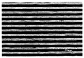
- the electron micrograph which shows the shape of the polysilicon film in embodiment.
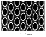
- the electron micrograph which shows the shape of the 2nd photoresist pattern in embodiment.
- the electron micrograph which shows the shape of the 2nd photoresist pattern which reduced the hole diameter in embodiment.
- 9 is a flowchart showing a process of a method for manufacturing a semiconductor device of a comparative example.
- the flowchart which shows the process of the manufacturing method of the semiconductor device of another comparative example.
- FIG. 1 schematically shows an enlarged part of a semiconductor wafer as a substrate according to an embodiment of the present invention, and shows steps of a method for manufacturing a semiconductor device according to the embodiment.
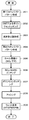
- FIG. 2 is a flowchart showing the steps of the semiconductor device manufacturing method according to the embodiment.
- a polysilicon film 101 as an etching target film is formed on the semiconductor wafer 100. Then, after forming the antireflection film 102 on the polysilicon film 101, a photoresist layer is formed on the antireflection film 102, and exposed and developed to form a first photoresist pattern 103 having a line and space shape. (Step 201 in FIG. 2). In addition, the shape of the 1st photoresist pattern 103 seen from the upper surface is typically shown in the upper part of Fig.1 (a).
- the pitch of the first photoresist pattern 103 is about 80 nm to 100 nm (line width 40 nm to 50 nm), for example, and the formation of the first photoresist pattern 103 can be performed by ArF immersion exposure, for example. it can.
- a line-and-line having a line width of about half (about 20 nm) of the first photoresist pattern 103 is formed by side wall transfer based on the first photoresist pattern 103 described above.
- a space pattern mask is formed, and the polysilicon film 101 is etched in a line-and-space manner (step 202 in FIG. 2).
- 1B schematically shows the shape of the polysilicon film 101 as viewed from above.
- FIG. 3 shows an electron micrograph showing the shape of the polysilicon film 101 actually produced.
- the first photoresist pattern 103 is slimmed, a silicon dioxide film or the like is formed on the side wall portion thereof, and then the first photoresist pattern 103 is removed, whereby the first first photoresist pattern 103 is removed.
- a line-and-space pattern mask having a line width and pitch that is about half or less than 103 can be formed.
- other double patterning techniques such as well-known LLE (Litho-Litho-Etch) and LLE (Litho-Etch-Litho-Etch) may be used instead of the sidewall transfer.
- an antireflection film 104 is formed on the polysilicon film 101 etched in a line-and-space manner (step 203 in FIG. 2).
- a photoresist layer is formed on the antireflection film 104 and exposed and developed to form a second photoresist pattern 105 having a hole shape (step 204 in FIG. 2). ).
- the hole diameter of the second photoresist pattern 105 is, for example, about 50 nm, and the formation of the second photoresist pattern 105 can be performed by, for example, ArF immersion exposure.
- FIG. 4 shows an electron micrograph showing the shape of the second photoresist pattern 105 actually created. As shown in this electron micrograph, in this embodiment, the hole shape is elliptical.
- a silicon dioxide (SiO 2 ) film (insulating film) 106 including the inside of the hole of the second photoresist pattern 105 is formed, and a reduction process for reducing the hole diameter is performed.
- Step 205 in FIG. 2 it is preferable to use an MLD (Molecular Layer Deposition) method capable of forming the silicon dioxide film 106 at a low temperature (140 ° C. or lower).
- the insulating film for reducing the hole diameter is not limited to a silicon dioxide film, but may be any film that can be formed at a temperature lower than the glass transition temperature of the resist so as not to damage the photoresist when the insulating film is formed.
- an aluminum oxide (Al 2 O 3 ) film, an aluminum nitride (AlN) film, a titanium oxide (TiO 2 ) film, an amorphous silicon film, or other metal oxide (HfO 2 , ZrO 2, etc.), silicon nitride ( SiN (can be formed by single wafer plasma)), SiON, or the like may be used.
- FIG. 5 shows an electron micrograph showing the shape of the second photoresist pattern 105 in which the hole diameter is actually reduced. In the case of the example shown in FIG. 5, the hole diameter is reduced to about 20 nm.
- anisotropic etching by RIE leaves the silicon dioxide film 106 on the side wall in the hole, leaving the upper surface of the second photoresist pattern 105 and the silicon dioxide film 106 on the bottom of the hole. Then, the antireflection film 104 at the bottom of the hole is removed by etching (step 206 in FIG. 2).
- the polysilicon layer 101 is etched using the second photoresist pattern 105 and the silicon dioxide film 106 in the hole as a mask (step 207 in FIG. 2).
- the second photoresist pattern 105 and the antireflection film 104 are removed by etching (ashing) (step 208 in FIG. 2).
- the etching process of the silicon dioxide film 106 and the antireflection film 104, the etching process of the polysilicon layer 101, and the etching (ashing) process of the second photoresist pattern 105 and the antireflection film 104 include, for example, an upper electrode and a lower part.
- a CCP etching apparatus that generates plasma by applying high-frequency power between the electrodes, a series of continuous processes can be performed according to the following recipe.
- the remaining silicon dioxide film 106 is removed by wet cleaning using hydrofluoric acid, SPM (sulfuric acid / hydrogen peroxide), APM (ammonia / hydrogen peroxide), or the like. (Step 209 in FIG. 2).
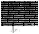
- FIG. 6 shows an electron micrograph showing the shape of the polysilicon island pattern actually formed.
- a polysilicon island pattern having a shape obtained by cutting a line-shaped pattern having a line width and a distance of about 20 nm so as to have a distance of about 20 nm could be formed.
- Such a polysilicon island pattern can be used as a gate layer of an SRAM, for example.
- a desired fine pattern can be formed with higher accuracy and efficiency than in the past.
- a silicon dioxide (SiO 2 ) film (insulating film) 106 including the inside of the hole of the second photoresist pattern 105 is formed, and a reduction step (step 205 in FIG. 2) for reducing the hole diameter is performed.
- the second photoresist pattern 105 may be slimmed. By performing slimming in this way, the intermediate exposure region of the photoresist is selectively removed, the pattern shape can be improved, and the scum (resist residue) at the bottom of the hole can be removed.
- the hole shape of the second photoresist pattern 105 in the shape of the second photoresist pattern 105 with the hole diameter reduced as shown in FIG.
- the ratio to the (minor axis) can be controlled, and by slimming, the shape after the reduction process can be made to be a more elongated shape (short in the lateral dimension).
- the vertical dimension / lateral dimension 3.74.
- This slimming process may be performed continuously by a wet process using a coating / developing apparatus after the second photoresist pattern 105 is formed, and a batch processing furnace is formed before the silicon dioxide (SiO 2 ) film (insulating film) 106 is formed. May be performed in a dry process.
- the dry process can be performed using oxygen plasma (for example, capacitively coupled plasma having an oxygen gas flow rate of 1000 sccm, a pressure of 20 Pa (150 mTorr), and a high frequency power of about 50 W).
- oxygen plasma for example, capacitively coupled plasma having an oxygen gas flow rate of 1000 sccm, a pressure of 20 Pa (150 mTorr), and a high frequency power of about 50 W.
- a slimming agent a solvent that does not melt the resist directly
- baking around 70 ° C. (resist surface layer portion is made slightly acidic)
- step 705 in FIG. 7 after performing chemical shrink (step 705 in FIG. 7), the antireflection film is etched (step 706 in FIG. 7), and then polysilicon is etched (step 707 in FIG. 7).
- step 805 in FIG. 8 after performing the anti-reflection film etching (step 805 in FIG. 8), chemical shrinking is performed (step 806 in FIG. 8), and then polysilicon etching (step 807 in FIG. 8) is performed.
- step 807 in FIG. 8 After performing the anti-reflection film etching (step 805 in FIG. 8), chemical shrinking is performed (step 806 in FIG. 8), and then polysilicon etching (step 807 in FIG. 8) is performed.
- step 807 in FIG. 8 After performing the anti-reflection film etching (step 805 in FIG. 8), chemical shrinking is performed (step 806 in FIG. 8), and then polysilicon etching (step 807 in FIG. 8) is performed.
- FIG. 10 shows the result of investigating the difference between the case where the elliptical hole is shrunk by the MLD of the silicon dioxide film (SiO 2 film) in this embodiment and the case where it is chemically shrunk.
- FIG. 11 is a graph showing the relationship between the shrinkage and the hole size, with the vertical axis representing the hole size and the horizontal axis representing the shrinkage.
- the hole size can be shrunk while maintaining an elliptical shape, but in the case of chemical shrinking, in the X direction The shrinkage amount increased, the hole shape approached a perfect circle shape, and the elliptical shape could not be maintained.
- the polysilicon film 101 is a linear line and space pattern has been described.
- the pattern may have a shape bent substantially at a right angle.
- FIG. 14 it can be used for logic patterning.
- a photoresist pattern bent at a substantially right angle is formed, and as shown in FIG. 14 (b), this pattern is narrowed by sidewall transfer.
- the polysilicon is etched.
- a mask for cutting the pattern is formed of a photoresist, and after shrinking with an insulating film as shown in FIG. Etch silicon.
- the semiconductor device manufacturing method of the present invention can be used in the field of manufacturing semiconductor devices. Therefore, it has industrial applicability.
- SYMBOLS 100 Semiconductor wafer, 101 ... Polysilicon layer, 102 ... Antireflection film (BARC), 103 ... First photoresist pattern, 104 ... Antireflection film (BARC), 105 ... Second photoresist pattern 106 Silicon dioxide film.
- BARC Antireflection film
- BARC Antireflection film
Landscapes
- Drying Of Semiconductors (AREA)
- Internal Circuitry In Semiconductor Integrated Circuit Devices (AREA)
- Semiconductor Memories (AREA)
Abstract
Description
処理ガス:CF4=200sccm
高周波電力(上部電極/下部電極):600W/100W
圧力:2.66Pa(20mTorr)
温度(天井部/側壁部/ウエハ載置台):80℃/60℃/30℃
時間:45秒
処理ガス:HBr/CF4/Ar=380/50/100sccm
高周波電力(上部電極/下部電極):300W/100W
圧力:2.66Pa(20mTorr)
温度(天井部/側壁部/ウエハ載置台):80℃/60℃/60℃
時間:180秒
処理ガス:O2=350sccm
高周波電力(上部電極/下部電極):300W/100W
圧力:13.3Pa(100mTorr)
温度(天井部/側壁部/ウエハ載置台):80℃/60℃/60℃
時間:180秒
Claims (10)
- 基板上に薄膜を形成する工程と、
前記薄膜上に、楕円ホールパターンの形成されたフォトレジストマスクを形成するレジストマスク形成工程と、
前記楕円ホールパターンの側壁に絶縁膜を形成することにより、前記楕円ホールパターンのホール径を縮小する縮小工程と、
前記ホール径を縮小した楕円ホールパターンを形成する前記フォトレジスト層と前記絶縁膜をマスクとして前記薄膜をエッチングする工程と
を備えたことを特徴とする半導体装置の製造方法。 - 基板上に成膜された薄膜を第1のパターンに基づいてエッチングする第1のエッチング工程と、
前記薄膜に形成された前記第1のパターンを埋める第1の成膜工程と、
前記第1のパターンの上に、第2のパターンが形成されたフォトレジストマスクを形成するマスク形成工程と、
前記フォトレジストマスクの前記第2のパターン内の側壁に絶縁膜を形成することにより前記第2のパターンのホール径を縮小する縮小工程と、
前記ホール径の縮小した第2のパターンを形成する前記フォトレジスト層と前記絶縁膜をマスクとして前記薄膜をエッチングする工程と
を備えたことを特徴とする半導体装置の製造方法。 - 前記絶縁膜は、酸化シリコン(SiO2)、窒化シリコン(SiN)、酸化アルミニウム(Al2O3)、窒化アルミニウム(AlN)、酸化チタン(TiO2)、アモルファスシリコンのいずれかを含むことを特徴とする請求項2に記載の半導体装置の製造方法。
- 前記絶縁膜は、140℃以下の温度で形成されることを特徴とする請求項2又は3に記載の半導体装置の製造方法。
- 前記縮小工程の前に、前記第2のパターンをスリミングするスリミング工程を含むことを特徴とする請求項2乃至4いずれか1項記載の半導体装置の製造方法。
- 半導体ウエハ基板上に成膜されたポリシリコン膜を、前記ポリシリコン膜に形成した少なくとも一部が平行な第1のパターンを有するフォトレジストに基づいてエッチングすることで、前記第1の平行パターンを有するポリシリコンを形成する工程と、
前記ポリシリコンの第1のパターンを反射防止膜で埋める工程と、
前記第1のパターンの上に第2のパターンを有するフォトレジストを形成する工程と、
前記フォトレジストの上に絶縁膜を形成することにより前記第2のパターンのホールの径を縮小する工程と、
前記縮小した第2のパターンを形成する前記フォトレジストと前記絶縁膜をマスクとして前記ホールの底の前記絶縁膜と前記反射防止膜とをエッチングして前記ポリシリコン膜を露出させる露出工程と、
前記露出工程で得られた新たなホールに基づいて前記ポリシリコン膜をエッチングすることで、ポリシリコンのパターンを形成するエッチング工程と
を備えたことを特徴とする半導体装置の製造方法。 - 前記絶縁膜は、酸化シリコン(SiO2)、窒化シリコン(SiN)、酸化アルミニウム(Al2O3)、窒化アルミニウム(AlN)、酸化チタン(TiO2)、アモルファスシリコンのいずれかを含むことを特徴とする請求項6に記載の半導体装置の製造方法。
- 前記絶縁膜は、140℃以下の温度で形成されることを特徴とする請求項6又は7に記載の半導体装置の製造方法。
- 前記ポリシリコン上の反射防止膜及びフォトレジストをアッシングとウェット洗浄により除去する工程
を備えたことを特徴とする請求項6乃至8いずれか1項記載の半導体装置の製造方法。 - 前記縮小工程の前に、前記第2のパターンをスリミングするスリミング工程を含むことを特徴とする請求項6乃至9いずれか1項記載の半導体装置の製造方法。
Priority Applications (3)
| Application Number | Priority Date | Filing Date | Title |
|---|---|---|---|
| JP2011526333A JPWO2011102140A1 (ja) | 2010-02-19 | 2011-02-18 | 半導体装置の製造方法 |
| US13/259,764 US20120028471A1 (en) | 2010-02-19 | 2011-02-18 | Method of manufacturing a semiconductor device |
| CN2011800029466A CN102473635A (zh) | 2010-02-19 | 2011-02-18 | 半导体装置的制造方法 |
Applications Claiming Priority (2)
| Application Number | Priority Date | Filing Date | Title |
|---|---|---|---|
| JP2010035294 | 2010-02-19 | ||
| JP2010-035294 | 2010-02-19 |
Publications (1)
| Publication Number | Publication Date |
|---|---|
| WO2011102140A1 true WO2011102140A1 (ja) | 2011-08-25 |
Family
ID=44482745
Family Applications (1)
| Application Number | Title | Priority Date | Filing Date |
|---|---|---|---|
| PCT/JP2011/000901 Ceased WO2011102140A1 (ja) | 2010-02-19 | 2011-02-18 | 半導体装置の製造方法 |
Country Status (6)
| Country | Link |
|---|---|
| US (1) | US20120028471A1 (ja) |
| JP (1) | JPWO2011102140A1 (ja) |
| KR (1) | KR20120091453A (ja) |
| CN (1) | CN102473635A (ja) |
| TW (1) | TW201203313A (ja) |
| WO (1) | WO2011102140A1 (ja) |
Cited By (3)
| Publication number | Priority date | Publication date | Assignee | Title |
|---|---|---|---|---|
| JP2014175509A (ja) * | 2013-03-11 | 2014-09-22 | Hitachi Kokusai Electric Inc | 半導体装置の製造方法、基板処理方法、基板処理装置およびプログラム |
| JP2020088174A (ja) * | 2018-11-26 | 2020-06-04 | 東京エレクトロン株式会社 | エッチング方法及び基板処理装置 |
| JP2022029847A (ja) * | 2020-08-05 | 2022-02-18 | 株式会社アルバック | シリコンのドライエッチング方法 |
Families Citing this family (10)
| Publication number | Priority date | Publication date | Assignee | Title |
|---|---|---|---|---|
| US8097175B2 (en) | 2008-10-28 | 2012-01-17 | Micron Technology, Inc. | Method for selectively permeating a self-assembled block copolymer, method for forming metal oxide structures, method for forming a metal oxide pattern, and method for patterning a semiconductor structure |
| US8404124B2 (en) | 2007-06-12 | 2013-03-26 | Micron Technology, Inc. | Alternating self-assembling morphologies of diblock copolymers controlled by variations in surfaces |
| US8999492B2 (en) | 2008-02-05 | 2015-04-07 | Micron Technology, Inc. | Method to produce nanometer-sized features with directed assembly of block copolymers |
| US8426313B2 (en) | 2008-03-21 | 2013-04-23 | Micron Technology, Inc. | Thermal anneal of block copolymer films with top interface constrained to wet both blocks with equal preference |
| US8425982B2 (en) | 2008-03-21 | 2013-04-23 | Micron Technology, Inc. | Methods of improving long range order in self-assembly of block copolymer films with ionic liquids |
| US8900963B2 (en) | 2011-11-02 | 2014-12-02 | Micron Technology, Inc. | Methods of forming semiconductor device structures, and related structures |
| US9087699B2 (en) | 2012-10-05 | 2015-07-21 | Micron Technology, Inc. | Methods of forming an array of openings in a substrate, and related methods of forming a semiconductor device structure |
| US9229328B2 (en) * | 2013-05-02 | 2016-01-05 | Micron Technology, Inc. | Methods of forming semiconductor device structures, and related semiconductor device structures |
| US9177795B2 (en) | 2013-09-27 | 2015-11-03 | Micron Technology, Inc. | Methods of forming nanostructures including metal oxides |
| WO2015117676A1 (en) * | 2014-02-07 | 2015-08-13 | Telefonaktiebolaget L M Ericsson (Publ) | Virtualized application cluster |
Citations (4)
| Publication number | Priority date | Publication date | Assignee | Title |
|---|---|---|---|---|
| JP2008300740A (ja) * | 2007-06-01 | 2008-12-11 | Toshiba Corp | 半導体装置の製造方法 |
| JP2009044090A (ja) * | 2007-08-10 | 2009-02-26 | Tokyo Electron Ltd | 半導体装置の製造方法及び記憶媒体 |
| JP2009094279A (ja) * | 2007-10-09 | 2009-04-30 | Elpida Memory Inc | ホールパターンの形成方法および半導体装置の製造方法 |
| JP2009099938A (ja) * | 2007-09-28 | 2009-05-07 | Tokyo Electron Ltd | 半導体装置の製造方法、半導体装置の製造装置、制御プログラム及びプログラム記憶媒体 |
Family Cites Families (6)
| Publication number | Priority date | Publication date | Assignee | Title |
|---|---|---|---|---|
| US7265056B2 (en) * | 2004-01-09 | 2007-09-04 | Taiwan Semiconductor Manufacturing Company, Ltd. | Method for forming novel BARC open for precision critical dimension control |
| US7199005B2 (en) * | 2005-08-02 | 2007-04-03 | Micron Technology, Inc. | Methods of forming pluralities of capacitors |
| KR20070087728A (ko) * | 2005-08-29 | 2007-08-29 | 동부일렉트로닉스 주식회사 | 폴리머를 이용한 반도체 소자의 게이트 형성 방법 |
| KR100796512B1 (ko) * | 2006-07-31 | 2008-01-21 | 동부일렉트로닉스 주식회사 | 반도체 소자의 인덕터 형성 방법 |
| US7838341B2 (en) * | 2008-03-14 | 2010-11-23 | Ovonyx, Inc. | Self-aligned memory cells and method for forming |
| JP2010040849A (ja) * | 2008-08-06 | 2010-02-18 | Tokyo Ohka Kogyo Co Ltd | レジストパターン形成方法 |
-
2011
- 2011-02-18 KR KR1020127018061A patent/KR20120091453A/ko not_active Ceased
- 2011-02-18 TW TW100105399A patent/TW201203313A/zh unknown
- 2011-02-18 CN CN2011800029466A patent/CN102473635A/zh active Pending
- 2011-02-18 US US13/259,764 patent/US20120028471A1/en not_active Abandoned
- 2011-02-18 WO PCT/JP2011/000901 patent/WO2011102140A1/ja not_active Ceased
- 2011-02-18 JP JP2011526333A patent/JPWO2011102140A1/ja active Pending
Patent Citations (4)
| Publication number | Priority date | Publication date | Assignee | Title |
|---|---|---|---|---|
| JP2008300740A (ja) * | 2007-06-01 | 2008-12-11 | Toshiba Corp | 半導体装置の製造方法 |
| JP2009044090A (ja) * | 2007-08-10 | 2009-02-26 | Tokyo Electron Ltd | 半導体装置の製造方法及び記憶媒体 |
| JP2009099938A (ja) * | 2007-09-28 | 2009-05-07 | Tokyo Electron Ltd | 半導体装置の製造方法、半導体装置の製造装置、制御プログラム及びプログラム記憶媒体 |
| JP2009094279A (ja) * | 2007-10-09 | 2009-04-30 | Elpida Memory Inc | ホールパターンの形成方法および半導体装置の製造方法 |
Cited By (5)
| Publication number | Priority date | Publication date | Assignee | Title |
|---|---|---|---|---|
| JP2014175509A (ja) * | 2013-03-11 | 2014-09-22 | Hitachi Kokusai Electric Inc | 半導体装置の製造方法、基板処理方法、基板処理装置およびプログラム |
| JP2020088174A (ja) * | 2018-11-26 | 2020-06-04 | 東京エレクトロン株式会社 | エッチング方法及び基板処理装置 |
| JP2022029847A (ja) * | 2020-08-05 | 2022-02-18 | 株式会社アルバック | シリコンのドライエッチング方法 |
| JP7478059B2 (ja) | 2020-08-05 | 2024-05-02 | 株式会社アルバック | シリコンのドライエッチング方法 |
| US12217969B2 (en) | 2020-08-05 | 2025-02-04 | Ulvac, Inc | Silicon dry etching method |
Also Published As
| Publication number | Publication date |
|---|---|
| US20120028471A1 (en) | 2012-02-02 |
| KR20120091453A (ko) | 2012-08-17 |
| TW201203313A (en) | 2012-01-16 |
| CN102473635A (zh) | 2012-05-23 |
| JPWO2011102140A1 (ja) | 2013-06-17 |
Similar Documents
| Publication | Publication Date | Title |
|---|---|---|
| WO2011102140A1 (ja) | 半導体装置の製造方法 | |
| KR101691717B1 (ko) | 다중 막층을 갖는 스페이서를 형성하기 위한 에칭 방법 | |
| US7494882B2 (en) | Manufacturing a semiconductive device using a controlled atomic layer removal process | |
| JP4034164B2 (ja) | 微細パターンの作製方法及び半導体装置の製造方法 | |
| US8283258B2 (en) | Selective wet etching of hafnium aluminum oxide films | |
| TWI389202B (zh) | 半導體裝置之製造方法、半導體裝置之製造裝置、控制程式及程式記憶媒體 | |
| JP2009152243A (ja) | 半導体装置の製造方法 | |
| KR20120098487A (ko) | 반도체 장치의 제조 방법 | |
| TW201543564A (zh) | 半導體製程 | |
| CN112992669B (zh) | 半导体结构及其形成方法 | |
| CN103839783A (zh) | 自对准双重图形的形成方法 | |
| CN106935484B (zh) | 半导体装置的制造方法 | |
| CN103928304B (zh) | 一种多晶硅上小尺寸图形结构的制备方法 | |
| JP4614995B2 (ja) | 半導体装置の製造方法 | |
| CN100517576C (zh) | 半导体器件的制造方法 | |
| JP5164446B2 (ja) | 半導体素子の微細パターン形成方法 | |
| CN104425228A (zh) | 多晶硅栅极的形成方法 | |
| US6989331B2 (en) | Hard mask removal | |
| CN103928313B (zh) | 一种小尺寸图形的制作方法 | |
| JP2010062212A (ja) | 半導体装置の製造方法 | |
| CN101290909A (zh) | 栅介电层的制造方法 | |
| CN121057244A (zh) | 鳍式场效应晶体管中鳍片结构的制备方法和鳍片结构 | |
| CN103903972A (zh) | 一种小尺寸图形的制作方法 | |
| KR20050068363A (ko) | 하드 마스크를 이용한 미세 패턴 형성 방법 | |
| JP2008053438A (ja) | 半導体装置の製造方法 |
Legal Events
| Date | Code | Title | Description |
|---|---|---|---|
| WWE | Wipo information: entry into national phase |
Ref document number: 201180002946.6 Country of ref document: CN |
|
| WWE | Wipo information: entry into national phase |
Ref document number: 2011526333 Country of ref document: JP |
|
| WWE | Wipo information: entry into national phase |
Ref document number: 13259764 Country of ref document: US |
|
| 121 | Ep: the epo has been informed by wipo that ep was designated in this application |
Ref document number: 11744431 Country of ref document: EP Kind code of ref document: A1 |
|
| ENP | Entry into the national phase |
Ref document number: 20127018061 Country of ref document: KR Kind code of ref document: A |
|
| NENP | Non-entry into the national phase |
Ref country code: DE |
|
| 122 | Ep: pct application non-entry in european phase |
Ref document number: 11744431 Country of ref document: EP Kind code of ref document: A1 |