WO2011058697A1 - 窒化物半導体素子の製造方法 - Google Patents
窒化物半導体素子の製造方法 Download PDFInfo
- Publication number
- WO2011058697A1 WO2011058697A1 PCT/JP2010/006159 JP2010006159W WO2011058697A1 WO 2011058697 A1 WO2011058697 A1 WO 2011058697A1 JP 2010006159 W JP2010006159 W JP 2010006159W WO 2011058697 A1 WO2011058697 A1 WO 2011058697A1
- Authority
- WO
- WIPO (PCT)
- Prior art keywords
- growth
- molar ratio
- layer
- plane
- supply molar
- Prior art date
Links
Images


Classifications
-
- H—ELECTRICITY
- H01—ELECTRIC ELEMENTS
- H01S—DEVICES USING THE PROCESS OF LIGHT AMPLIFICATION BY STIMULATED EMISSION OF RADIATION [LASER] TO AMPLIFY OR GENERATE LIGHT; DEVICES USING STIMULATED EMISSION OF ELECTROMAGNETIC RADIATION IN WAVE RANGES OTHER THAN OPTICAL
- H01S5/00—Semiconductor lasers
- H01S5/30—Structure or shape of the active region; Materials used for the active region
- H01S5/34—Structure or shape of the active region; Materials used for the active region comprising quantum well or superlattice structures, e.g. single quantum well [SQW] lasers, multiple quantum well [MQW] lasers or graded index separate confinement heterostructure [GRINSCH] lasers
- H01S5/343—Structure or shape of the active region; Materials used for the active region comprising quantum well or superlattice structures, e.g. single quantum well [SQW] lasers, multiple quantum well [MQW] lasers or graded index separate confinement heterostructure [GRINSCH] lasers in AIIIBV compounds, e.g. AlGaAs-laser, InP-based laser
- H01S5/34333—Structure or shape of the active region; Materials used for the active region comprising quantum well or superlattice structures, e.g. single quantum well [SQW] lasers, multiple quantum well [MQW] lasers or graded index separate confinement heterostructure [GRINSCH] lasers in AIIIBV compounds, e.g. AlGaAs-laser, InP-based laser with a well layer based on Ga(In)N or Ga(In)P, e.g. blue laser
-
- B—PERFORMING OPERATIONS; TRANSPORTING
- B82—NANOTECHNOLOGY
- B82Y—SPECIFIC USES OR APPLICATIONS OF NANOSTRUCTURES; MEASUREMENT OR ANALYSIS OF NANOSTRUCTURES; MANUFACTURE OR TREATMENT OF NANOSTRUCTURES
- B82Y20/00—Nanooptics, e.g. quantum optics or photonic crystals
-
- H—ELECTRICITY
- H01—ELECTRIC ELEMENTS
- H01L—SEMICONDUCTOR DEVICES NOT COVERED BY CLASS H10
- H01L21/00—Processes or apparatus adapted for the manufacture or treatment of semiconductor or solid state devices or of parts thereof
- H01L21/02—Manufacture or treatment of semiconductor devices or of parts thereof
- H01L21/02104—Forming layers
- H01L21/02365—Forming inorganic semiconducting materials on a substrate
- H01L21/02367—Substrates
- H01L21/0237—Materials
- H01L21/02373—Group 14 semiconducting materials
- H01L21/02378—Silicon carbide
-
- H—ELECTRICITY
- H01—ELECTRIC ELEMENTS
- H01L—SEMICONDUCTOR DEVICES NOT COVERED BY CLASS H10
- H01L21/00—Processes or apparatus adapted for the manufacture or treatment of semiconductor or solid state devices or of parts thereof
- H01L21/02—Manufacture or treatment of semiconductor devices or of parts thereof
- H01L21/02104—Forming layers
- H01L21/02365—Forming inorganic semiconducting materials on a substrate
- H01L21/02518—Deposited layers
- H01L21/02521—Materials
- H01L21/02538—Group 13/15 materials
- H01L21/0254—Nitrides
-
- H—ELECTRICITY
- H01—ELECTRIC ELEMENTS
- H01L—SEMICONDUCTOR DEVICES NOT COVERED BY CLASS H10
- H01L21/00—Processes or apparatus adapted for the manufacture or treatment of semiconductor or solid state devices or of parts thereof
- H01L21/02—Manufacture or treatment of semiconductor devices or of parts thereof
- H01L21/02104—Forming layers
- H01L21/02365—Forming inorganic semiconducting materials on a substrate
- H01L21/02612—Formation types
- H01L21/02617—Deposition types
- H01L21/0262—Reduction or decomposition of gaseous compounds, e.g. CVD
-
- H—ELECTRICITY
- H01—ELECTRIC ELEMENTS
- H01L—SEMICONDUCTOR DEVICES NOT COVERED BY CLASS H10
- H01L33/00—Semiconductor devices with at least one potential-jump barrier or surface barrier specially adapted for light emission; Processes or apparatus specially adapted for the manufacture or treatment thereof or of parts thereof; Details thereof
- H01L33/005—Processes
- H01L33/0062—Processes for devices with an active region comprising only III-V compounds
- H01L33/0075—Processes for devices with an active region comprising only III-V compounds comprising nitride compounds
-
- H—ELECTRICITY
- H01—ELECTRIC ELEMENTS
- H01L—SEMICONDUCTOR DEVICES NOT COVERED BY CLASS H10
- H01L33/00—Semiconductor devices with at least one potential-jump barrier or surface barrier specially adapted for light emission; Processes or apparatus specially adapted for the manufacture or treatment thereof or of parts thereof; Details thereof
- H01L33/005—Processes
- H01L33/0062—Processes for devices with an active region comprising only III-V compounds
- H01L33/0066—Processes for devices with an active region comprising only III-V compounds with a substrate not being a III-V compound
- H01L33/007—Processes for devices with an active region comprising only III-V compounds with a substrate not being a III-V compound comprising nitride compounds
-
- H—ELECTRICITY
- H01—ELECTRIC ELEMENTS
- H01L—SEMICONDUCTOR DEVICES NOT COVERED BY CLASS H10
- H01L33/00—Semiconductor devices with at least one potential-jump barrier or surface barrier specially adapted for light emission; Processes or apparatus specially adapted for the manufacture or treatment thereof or of parts thereof; Details thereof
- H01L33/02—Semiconductor devices with at least one potential-jump barrier or surface barrier specially adapted for light emission; Processes or apparatus specially adapted for the manufacture or treatment thereof or of parts thereof; Details thereof characterised by the semiconductor bodies
- H01L33/16—Semiconductor devices with at least one potential-jump barrier or surface barrier specially adapted for light emission; Processes or apparatus specially adapted for the manufacture or treatment thereof or of parts thereof; Details thereof characterised by the semiconductor bodies with a particular crystal structure or orientation, e.g. polycrystalline, amorphous or porous
-
- H—ELECTRICITY
- H01—ELECTRIC ELEMENTS
- H01L—SEMICONDUCTOR DEVICES NOT COVERED BY CLASS H10
- H01L33/00—Semiconductor devices with at least one potential-jump barrier or surface barrier specially adapted for light emission; Processes or apparatus specially adapted for the manufacture or treatment thereof or of parts thereof; Details thereof
- H01L33/02—Semiconductor devices with at least one potential-jump barrier or surface barrier specially adapted for light emission; Processes or apparatus specially adapted for the manufacture or treatment thereof or of parts thereof; Details thereof characterised by the semiconductor bodies
- H01L33/26—Materials of the light emitting region
- H01L33/30—Materials of the light emitting region containing only elements of group III and group V of the periodic system
- H01L33/32—Materials of the light emitting region containing only elements of group III and group V of the periodic system containing nitrogen
-
- H—ELECTRICITY
- H01—ELECTRIC ELEMENTS
- H01S—DEVICES USING THE PROCESS OF LIGHT AMPLIFICATION BY STIMULATED EMISSION OF RADIATION [LASER] TO AMPLIFY OR GENERATE LIGHT; DEVICES USING STIMULATED EMISSION OF ELECTROMAGNETIC RADIATION IN WAVE RANGES OTHER THAN OPTICAL
- H01S2304/00—Special growth methods for semiconductor lasers
- H01S2304/04—MOCVD or MOVPE
Definitions
- the present invention relates to a method for manufacturing a gallium nitride compound semiconductor and a semiconductor light emitting device manufactured by the manufacturing method.
- a nitride semiconductor having nitrogen (N) as a group V element is considered promising as a material for a short-wavelength light-emitting element because of its band gap.
- gallium nitride compound semiconductors GaN-based semiconductors
- LEDs blue light-emitting diodes
- semiconductor lasers made of GaN-based semiconductors have been put into practical use.
- FIG. 1 schematically shows a unit cell of GaN.
- Al a Ga b In C N ( 0 ⁇ a, b, c ⁇ 1, a + b + c 1) semiconductor crystal, some of the Ga shown in FIG. 1 may be replaced by Al and / or In.
- FIG. 2 shows four basic vectors a 1 , a 2 , a 3 , and c that are generally used to represent the surface of the wurtzite crystal structure in the 4-index notation (hexagonal crystal index).
- the basic vector c extends in the [0001] direction, and this direction is called “c-axis”.
- a plane perpendicular to the c-axis is called “c-plane” or “(0001) plane”.
- c-axis” and “c-plane” may be referred to as “C-axis” and “C-plane”, respectively.
- FIG. 3 there are typical crystal plane orientations other than the c-plane.
- 3 (a) is the (0001) plane
- FIG. 3 (b) is the (10-10) plane
- FIG. 3 (c) is the (11-20) plane
- FIG. 3 (d) is the (10-12) plane.
- “-” attached to the left of the number in parentheses representing the Miller index means “bar”.
- the (0001) plane, (10-10) plane, (11-20) plane, and (10-12) plane are the c-plane, m-plane, a-plane, and r-plane, respectively.
- the m-plane and a-plane are “nonpolar planes” parallel to the c-axis, while the r-plane is a “semipolar plane”.
- the m-plane is a general term for the (10-10) plane, the (-1010) plane, the (1-100) plane, the (-1100) plane, the (01-10) plane, and the (0-110) plane.
- the X plane may be referred to as a “growth plane”.
- a semiconductor layer formed by X-plane growth may be referred to as an “X-plane semiconductor layer”.
- spontaneous polarization spontaneous polarization resulting from the shift of Ga atoms and N atoms in the c-axis direction on the c-plane is ⁇ c. Occurs in the direction.
- piezoelectric polarization due to strain occurs in the + c direction, and a quantum confinement Stark effect of carriers is generated, which is called a “polar plane”.
- the emission recombination probability of carriers in the light emitting part is reduced and the internal quantum efficiency is reduced, so that the threshold current is increased in the semiconductor laser, and in the case of the LED, the power consumption is increased and the light emission efficiency is decreased. It is.
- the piezo electric field is screened as the injected carrier density is increased, and the emission wavelength is also changed.
- gallium nitride-based compound semiconductors on nonpolar surfaces such as m-plane and a-plane, or semipolar planes such as r-plane. If a nonpolar plane can be selected as the growth plane, polarization does not occur in the layer thickness direction (crystal growth direction) of the light-emitting portion, so that no quantum confined Stark effect occurs, and a potentially high-efficiency light-emitting element can be manufactured. Even when the semipolar plane is selected as the growth plane, the contribution of the quantum confined Stark effect can be greatly reduced.
- Patent Document 1 discloses that In x Ga 1-x N (0 ⁇ 1 ) is based on a characteristic diagram regarding a molar ratio of an In-containing source gas (In supply molar ratio), a crystal growth temperature (growth temperature), and an emission wavelength. A technique for obtaining optimum growth conditions in the x ⁇ 1) layer is disclosed.
- the drawing of Patent Document 1 shows a graph in which the horizontal axis represents the molar ratio of the In source gas to the group III source gas, and the vertical axis represents the emission wavelength. This graph shows a characteristic curve in consideration of the growth temperature.
- Patent Document 1 discloses a method for determining an optimum condition in c-plane growth of an In x Ga 1-x N (0 ⁇ x ⁇ 1) layer.
- the method disclosed in Patent Document 1 cannot be applied as it is to crystal growth of a nonpolar m-plane, a-plane, or semipolar r-plane. That is, there is no known growth condition optimization method applicable to the nonpolar m-plane, a-plane, or semipolar r-plane.
- the present invention has been made to solve the above-described problems, and its object is to improve the crystallinity and light emission efficiency of InGaN in a method for crystal growth other than c-plane growth.
- the method for producing a gallium nitride compound semiconductor light emitting device of the present invention includes a step of forming a gallium nitride compound semiconductor layer having a nonpolar or semipolar main surface by a metal organic chemical vapor deposition method.
- the parameters that define the growth conditions of the metal organic chemical vapor deposition method are pressure, growth rate, growth temperature, and supply molar ratio of In source gas contained in the group III source gas.
- A the In supply molar ratio
- a plurality of In y Ga 1-y N (0 ⁇ y ⁇ 1) layers whose main surface is a nonpolar surface or a semipolar surface are different by metal organic vapor phase epitaxy.
- Step (a1) of forming under growth conditions and In x Ga 1-x N (0 ⁇ x ⁇ 1) having the same emission wavelength among the plurality of In y Ga 1-y N (0 ⁇ y ⁇ 1) layers The step (a2) for obtaining the relationship between the growth temperature and the In supply molar ratio when the pressure and the growth rate are constant based on the growth conditions for forming the layer, and the relationship between the growth temperature and the In supply molar ratio are shown.
- the step (a2) includes the step of determining the relationship between the growth temperature and the In supply molar ratio when the pressure and the growth rate are constant for each of the different combinations of pressure and growth rate.
- the In x Ga 1-x N (0 ⁇ x ⁇ 1) layer is a single quantum well light emitting layer or a well layer included in a multiple quantum well light emitting layer.
- the well layer has a thickness of 2 nm to 20 nm.
- the thickness of the well layer is 6 nm or more and 16 nm or less.
- step (B) includes the step (b1) of adjusting the growth pressure within the range of 200 Torr to 600 Torr, wherein in step (B) the adjusted growth pressure and the selected growth rate.
- the In x Ga 1-x N (0 ⁇ x ⁇ 1) layer is grown at the growth temperature and the In supply molar ratio corresponding to the saturation point on the curve showing the relationship between the growth temperature and the In supply molar ratio.
- step (B) comprises the step (b1) of adjusting the growth pressure to atmospheric pressure, the growth obtained in step (B) for the adjusted growth pressure and the selected growth rate.
- An In x Ga 1-x N (0 ⁇ x ⁇ 1) layer is grown at a growth temperature and an In supply molar ratio corresponding to the saturation point on the curve indicating the relationship between temperature and In supply molar ratio.
- the growth condition determining method for a gallium nitride compound semiconductor layer according to the present invention is a method for determining a condition for growing a gallium nitride compound semiconductor layer whose main surface is a nonpolar surface or a semipolar surface by metal organic vapor phase epitaxy.
- a method for determining the growth conditions of a compound semiconductor layer, the parameters defining the growth conditions of the metal organic chemical vapor deposition method are pressure, growth rate, growth temperature, and supply moles of In source gas contained in the group III source gas.
- a plurality of In y Ga 1-y N (0 ⁇ y ⁇ 1) layers whose main surface is a nonpolar surface or a semipolar surface are grown differently by metalorganic vapor phase epitaxy, including the In supply molar ratio.
- Step (a1) formed under conditions, and an In x Ga 1-x N (0 ⁇ x ⁇ 1) layer having the same emission wavelength among the plurality of In y Ga 1-y N (0 ⁇ y ⁇ 1) layers Pressure and growth based on the growth conditions
- the step (a2) for obtaining the relationship between the growth temperature and the In supply molar ratio when the rate is constant, and on the curve indicating the relationship between the growth temperature and the In supply molar ratio the growth temperature increases the In supply molar ratio.
- (a3) determining a saturation point between a monotonically increasing region and a saturated region.
- the step (a1) and the step (a2) include a step of forming a first In x1 Ga 1-x1 N (0 ⁇ x1 ⁇ 1) layer at a first In supply molar ratio,
- the first In x1 Ga 1-x1 N (0 ⁇ x1 ⁇ 1) layer is grown at the same growth temperature as that at the second In supply molar ratio lower than the first In supply molar ratio.
- a step of forming a second In x2 Ga 1-x2 N (0 ⁇ x2 ⁇ 1) layer, and a growth temperature for forming the first In x1 Ga 1-x1 N (0 ⁇ x1 ⁇ 1) layer Forming a third In x3 Ga 1-x3 N (0 ⁇ x3 ⁇ 1) layer at a third In supply molar ratio lower than the second In supply molar ratio at the same growth temperature.
- step (a3) when x2 is equal to x1 and x3 is different from x2, the third In supply molar ratio is selected as the In supply molar ratio corresponding to the saturation point.
- the growth temperature and the mole of In source gas are increased. Since the parameters of the crystal growth conditions including the ratio can be appropriately determined, it is possible to form an In x Ga 1-x N crystal (0 ⁇ x ⁇ 1) that exhibits high emission efficiency at the target emission wavelength. Become.
- FIG. 1 It is a perspective view which shows typically the unit cell of GaN. It is a perspective view showing the basic vector a 1, a 2, a 3 , c wurtzite crystal structure.
- (A) to (d) are schematic views showing typical crystal plane orientations of a hexagonal wurtzite structure. Is a graph schematically showing the relationship between the growth temperature In feed mole ratio when the same In x Ga 1-x N of the light-emitting wavelength (0 ⁇ x ⁇ 1) layer formed by c-plane growth. Is a graph schematically showing the relationship between In feed mole ratio and PL emission intensity when the same In x Ga 1-x N of the light-emitting wavelength (0 ⁇ x ⁇ 1) layer formed by c-plane growth.
- the same In x Ga 1-x N of the light-emitting wavelength (0 ⁇ x ⁇ 1) layer is a graph schematically showing the In feed molar ratio dependence of the growth temperature and the PL emission intensity when forming the c-plane growth. It is a graph which shows typically the In supply molar ratio dependence of the growth temperature and PL luminescence intensity when forming an In x Ga 1-x N (0 ⁇ x ⁇ 1) layer having the same emission wavelength by m-plane growth. It is sectional drawing which showed typically the structure of the gallium nitride type compound semiconductor light-emitting device for evaluation in Embodiment 1 to 3 of this invention.
- FIG. 4 is a graph showing the dependence of the growth temperature ( ⁇ ) and emission intensity ( ⁇ ) on In supply molar ratio in Embodiment 1.
- 3 is a graph showing the dependence of the half-value width in the PL spectrum on the In supply molar ratio in Embodiment 1.
- 6 is a graph showing the dependence of the growth temperature ( ⁇ ) and emission intensity ( ⁇ ) on In supply molar ratio in Embodiment 2. It is a graph which shows the In supply molar ratio dependence of the growth temperature ((triangle
- FIG. It is a graph which shows typically the change of the characteristic curve by pressure. It is a graph which shows typically the change of the characteristic curve by a growth rate.
- FIG. (A) is a figure which shows typically the crystal structure (wurtzite type crystal structure) of a GaN-type compound semiconductor
- (b) is the relationship between the normal of m surface, + c-axis direction, and a-axis direction
- FIG. (A) And (b) is sectional drawing which shows the arrangement
- (A) And (b) is sectional drawing which shows typically the main surface and its vicinity area
- a gallium nitride compound semiconductor layer whose main surface is a nonpolar surface (for example, m-plane or a-plane) or a semipolar surface (for example, r-plane) is treated with an organic metal layer.
- a step of forming by a phase growth method is formed by adjusting parameters that define the growth conditions of the metal organic chemical vapor deposition method.
- the parameters defining the growth conditions include “pressure”, “growth rate”, “growth temperature”, and “supply molar ratio of In source gas contained in group III source gas (In supply molar ratio)”. .
- a source gas is supplied into a reaction chamber of an MOCVD apparatus, and an In x Ga 1-x N (0 ⁇ x ⁇ 1) layer whose main surface is a plane orientation having a lower In incorporation efficiency than the c-plane is grown. Execute the process.
- Specific examples of crystal planes whose In incorporation efficiency is lower than the c-plane are m-plane, a-plane, and r-plane.
- the present invention will be described in the case of performing m-plane growth.
- the present invention is not limited to m-plane growth and can be widely applied to the formation of In x Ga 1-x N (0 ⁇ x ⁇ 1) layers having crystal planes whose In incorporation efficiency is lower than the c-plane.
- a source gas containing In a source gas containing Ga
- a source gas containing Ga a source gas containing Ga
- a source gas containing N are supplied to the reaction chamber.
- the source gas containing In and the source gas containing Ga are group III source gases.
- the source gas containing N is a group V source gas.
- the “growth temperature” and the “In source gas contained in the group III source gas” Adjust the “feed molar ratio”.
- the supply molar ratio of the In source gas contained in the group III source gas is referred to as “In supply molar ratio”.
- the “In supply molar ratio” refers to the source gases of Ga and In which are group III atoms supplied to the reaction chamber during the growth of the In x Ga 1-x N (0 ⁇ x ⁇ 1) layer. Of each molar supply flow rate in 1 minute (mol / min).
- “In supply molar ratio” or “In-containing gas molar ratio” is the ratio of the molar flow rate of In source gas to the total molar supply rate of In source gas and Ga source gas supplied to the reaction chamber. It represents.
- the In source gas is, for example, trimethylindium (TMI), and “supply In source gas” is also expressed as [TMI].
- the Ga source gas is, for example, trimethylgallium (TMG) or triethylgallium (TEG).
- Ga source gas is also expressed as [TMG] or [TEG].
- [TMI] is the molar supply flow rate (mol / min) of TMI for 1 minute.
- [TMG] is the molar supply flow rate (mol / min) of TMG for 1 minute
- [TEG] is the molar supply flow rate (mol / min) of TEG for 1 minute.
- the molar flow rate of the source gas supplied to the reaction chamber is selected as one of the control factors for the In uptake rate. More specifically, as a control factor of the In composition x of the In x Ga 1-x N (0 ⁇ x ⁇ 1) layer, “pressure”, “growth temperature”, “In supply molar ratio”, and “growth rate” are set. Select as a control factor.
- the “In supply molar ratio” is expressed by [TMI] and [TMG].
- the growth rate is substantially determined by [TMG].
- a plurality of In y Ga 1-y N (0 ⁇ y ⁇ 1) layers whose main surface is a nonpolar surface or a semipolar surface are formed under different growth conditions. Based on the growth conditions for forming an In x Ga 1-x N (0 ⁇ x ⁇ 1) layer having the same emission wavelength among the plurality of In y Ga 1-y N (0 ⁇ y ⁇ 1) layers, The relationship between the growth temperature and the In supply molar ratio when the pressure and the growth rate are constant is obtained.
- the In composition ratio x in the In x Ga 1-x N (0 ⁇ x ⁇ 1) layer depends on both the “growth temperature” and the “In supply molar ratio” of the In x Ga 1-x N layer. Change. In other words, even if the “In supply molar ratio” is the same, the In composition ratio x in the In x Ga 1-x N (0 ⁇ x ⁇ 1) layer is different if the “growth temperature” is different. In addition, even if the “growth temperature” is the same, if the “In supply molar ratio” is different, the In composition ratio x in the growing In x Ga 1-x N (0 ⁇ x ⁇ 1) layer is different.
- the emission wavelength is determined by the In composition ratio x
- the “growth temperature” and the “In supply molar ratio” Both must be determined.
- the “growth temperature” and the “In supply molar ratio” are changed so as to move the “point” on the straight line (broken line) in FIG.
- the layer can be grown. That is, the In composition ratio x in the obtained In x Ga 1-x N layer is constant without depending on the position of the point on the straight line.
- FIG. 4B is a graph showing the relationship between the In supply molar ratio and the PL emission intensity.
- FIG. 4B shows that the PL emission intensity has the maximum value (peak value) at a certain In supply molar ratio.
- the reason why the PL emission intensity changes depending on a certain In supply molar ratio is that even if the In composition x of the In x Ga 1-x N (0 ⁇ x ⁇ 1) layer is the same, the “growth” This is because crystallinity changes depending on “temperature” and “In supply molar ratio”.
- the PL emission intensity shows the maximum value. Therefore, in order to form an In x Ga 1-x N (0 ⁇ x ⁇ 1) layer having excellent crystallinity by c-plane growth, it is not sufficient to obtain the relationship shown in FIG. 4A. It is necessary to obtain the relationship between the In supply molar ratio and the PL emission intensity shown in 4B.
- FIG. 4C shows the “In supply molar ratio” dependency of “PL emission intensity” shown in FIG. 4B and the straight line (broken line) showing the “In supply molar ratio” dependency of “growth temperature” shown in FIG. 4A. It is a graph which shows the curve (solid line) to show.
- the straight lines and curves shown in FIG. 4C have different shapes depending on the target emission wavelength. For this reason, the graph of FIG. 4C needs to be obtained by experiment for a desired emission wavelength.
- the graph of FIG. 4C needs to be obtained by experiment for a desired emission wavelength.
- a large number of samples satisfying the relationship between the “growth temperature” and the “In supply molar ratio” thus obtained were prepared, and the “growth temperature” and the “In supply molar ratio” at which the PL emission intensity was highest were tested. Need to find out.
- the inventor has increased the growth temperature of the In supply molar ratio unlike conventional c-plane growth. It has been found that there are a monotonically increasing region (monotonically increasing region) and a saturated region (saturating region). On this characteristic curve, a “saturation point” exists at the boundary between the monotonously increasing region and the saturated region.
- FIG. 5 is a graph schematically showing an example of conditions for forming an m-plane In x Ga 1-x N (0 ⁇ x ⁇ 1) layer according to the present invention, and corresponds to FIG. 4C.
- the vertical axis on the left side of the graph is the growth temperature, and the vertical axis on the right side is the PL emission intensity [arbitrary unit].
- a broken line in the graph is a curve (characteristic curve) showing a relationship between an In supply molar ratio and a growth temperature for forming an m-plane In x Ga 1-x N (0 ⁇ x ⁇ 1) layer having the same emission wavelength. is there.
- the In supply molar ratio corresponding to the point P on the broken line in FIG. 5 is, for example, 0.5, and the growth temperature corresponding to the point P is about 770 ° C.
- the target In composition ratio x In order to achieve the target In composition ratio x, it is necessary to set the two control factors of the In supply molar ratio and the growth temperature so as to satisfy the relationship of the characteristic curve. This characteristic curve changes even when the growth pressure is different. Further, it varies even if the target In composition ratio x is different. When the growth pressure and the target In composition ratio x are given, the shape of the characteristic curve is determined.
- the growth temperature increases monotonously as the In supply molar ratio increases, but when the In supply molar ratio is relatively high, the In supply Regardless of the size of the molar ratio, the growth temperature shows a substantially constant value.
- the former can be referred to as a “monotonically increasing region”, and the latter can be referred to as a “saturated region”.
- saturation point at the boundary between the monotonically increasing region and the saturated region. The shape of such a characteristic curve is greatly different from that of the c-plane growth characteristic curve.
- the present inventor has found through experiments that the PL emission intensity shows a peak when the In supply molar ratio and the growth temperature correspond to the saturation point on the characteristic curve. That is, if the In supply molar ratio and the growth temperature corresponding to the saturation point on the characteristic curve are found, the growth conditions necessary to maximize the PL emission intensity can be determined. Therefore, if a saturation point on the characteristic curve can be detected, an experiment for determining a condition for maximizing the PL emission intensity becomes unnecessary.
- the growth temperature monotonously increases as the In supply molar ratio increases, and does not have a feature point associated with the peak of PL emission intensity. For this reason, it is necessary to measure the PL emission intensity of these samples after producing a large number of samples having the target In composition ratio x by changing the In supply molar ratio and the growth temperature. For the first time, by measuring such PL emission intensity, it is possible to know the dependence of the PL emission intensity on the In supply molar ratio shown by the solid line in FIG. 4C, and to maximize the PL emission intensity and growth. It becomes possible to detect the temperature.
- the thickness of the active layer is preferably 3.0 mn or less because of the Stark effect on the polar surface. For this reason, the growth rate of the active layer must be about 4.0 nm / min or less.
- the growth rate of the active layer made of In x Ga 1-x N (0 ⁇ x ⁇ 1) is determined by the supply amount of Ga atoms. Therefore, In x G
- the growth rate of the a 1-x N (0 ⁇ x ⁇ 1) layer can be expressed by a function of [TMG].
- the thickness of the active layer can be increased from 3 nm and can be increased to about 20 nm. For this reason, the growth rate is increased to 4.5 nm / min or more, and crystal growth much faster than the growth rate in the c-plane growth becomes possible.
- the In supply molar ratio [TMI] / ([TMI] + [TMG]) is smaller than that in c-plane growth.
- FIG. 6 is a diagram schematically showing a cross-sectional structure of a sample (light-emitting element 10) used for obtaining the characteristic curve shown in FIG.
- the substrate 11 of the light emitting element 10 is a substrate on which (10-10) m-plane gallium nitride (GaN) can be grown.
- the substrate 11 is most preferably a GaN free-standing substrate having an m-plane as a main surface, but may be a substrate of silicon carbide (SiC) having a lattice constant close to that of the 4H, 6H structure and expressing the m-plane.
- SiC silicon carbide
- the sapphire substrate which exposed m surface may be sufficient.
- An underlayer (GaN layer) 12 made of undoped GaN and having a thickness of about 1.0 to 2.0 ⁇ m is formed on the substrate 11.
- a multiple quantum well in which barrier layers 13 made of undoped GaN having a thickness of about 30 nm and well layers (active layers) 14 made of In 0.1 Ga 0.9 N having a thickness of about 15 nm are alternately stacked on the underlayer 12.
- a light emitting layer 15 having a structure (MQW) is formed.
- the light emitting device 10 used in this experiment is formed of a light emitting layer 15 having a three-cycle multiple quantum well structure in which four GaN barrier layers 13 and three active layers 14 are formed.
- the thickness of the well layer (active layer) 14 made of In 0.1 Ga 0.9 N is generally about 2.0 to 20 nm in the nonpolar / semipolar plane.
- a preferable thickness of the well layer 14 is about 6.0 to 16 nm.
- the well layer 14 having a thickness of about 15 nm was employed, but a well layer having a thickness other than that may be used.
- the thickness of the barrier layer 13 is about 1.0 to 3.0 times the thickness of the active layer. In this experiment, the 30 nm-thickness barrier layer 13 was used, but the same result can be obtained even if the thickness of the barrier layer 13 is changed.
- the light emitting device 10 was manufactured by vapor phase growth by MOCVD.
- the growth pressure in the reaction chamber was set to 300 Torr, and the gases used were hydrogen (H 2 ), nitrogen (N 2 ) as carrier gases, trimethylgallium (TMG), trimethylindium (TMI), V Ammonia-based source gas is ammonia (NH 3 ).
- the substrate 11 is washed with a buffered hydrofluoric acid solution (BHF), and then sufficiently washed with water and dried. After cleaning, the substrate 11 is placed in the reaction chamber of the MOCVD apparatus so as not to be exposed to air as much as possible. Thereafter, the substrate 11 is heated to 850 ° C. while supplying ammonia (NH 3 ) gas as a nitrogen source, hydrogen (H 2 ) and nitrogen (N 2 ) as carrier gases, and the substrate surface is subjected to a cleaning process. Next, TMG or TEG is supplied and the substrate is heated to about 1100 ° C. to deposit the GaN layer 12. The growth rate for depositing the GaN layer 12 is about 10 to 40 nm / min.
- BHF buffered hydrofluoric acid solution
- the group III source gas TMG is stopped, and the carrier gas is also stopped with hydrogen and only nitrogen gas.
- the substrate temperature is lowered to about 700 to 800 ° C., and the GaN barrier layer 13 is deposited.
- the supply of TMI is started to deposit an In x Ga 1-x N (0 ⁇ x ⁇ 1) well layer 14.
- the GaN barrier layer 13 and the In x Ga 1-x N (0 ⁇ x ⁇ 1) well layer 14 are alternately deposited in three cycles or more to form the GaN / InGaN multiple quantum well light emitting layer 15 serving as a light emitting part. .
- thermocouple for measuring the growth temperature is surrounded by a current-heating type heater and is installed directly under the carbon susceptor.
- the growth temperature in this specification is a temperature measured by the thermocouple.
- the method for producing a gallium nitride-based compound semiconductor according to the present invention can be suitably carried out even with a device other than the apparatus used by the present inventor.
- substrate temperature are not limited to the method mentioned above.
- FIG. 7 is a graph showing a characteristic curve for forming the m-plane In 0.1 Ga 0.9 N well layer 14 having an emission wavelength of about 410 nm ⁇ 5 nm.
- This characteristic curve shows the relationship between the In supply molar ratio and the growth temperature obtained under the conditions where the pressure is set to 300 Torr and the growth rate is set to about 6.0 nm / min. .
- the target emission wavelength is about 410 nm ⁇ 5 nm.
- the In 0.1 Ga 0.9 N well layer 14 having an emission wavelength of about 410 nm ⁇ 5 nm in each case where the In supply molar ratio is 0.30, 0.40, 0.50, 0.60, and 0.83.
- the growth temperature was a value indicated by ⁇ in FIG.
- the vertical axis on the right side of the graph represents PL emission intensity ( ⁇ ) obtained by performing photoluminescence (PL) measurement on the light-emitting element 10 created under five different conditions.
- Table 1 shows the numerical data of points ⁇ and ⁇ in Fig. 7.
- the In supply molar ratio is 0.50 or more
- the separation of In proceeds to the extent that even if the In supply molar ratio is increased, it cannot be compensated. As a result, the emission wavelength becomes shorter than the target value. In other words, there is an upper limit on the growth temperature in this region. In this region, even if the In supply molar ratio is further increased, the amount of In incorporation into the crystal does not change. This phenomenon is considered to occur similarly in a plane orientation in which In incorporation is more difficult than c-plane growth due to low In incorporation efficiency.
- FIG. 7 shows that in the monotonically increasing region, the PL emission intensity increases as the In supply molar ratio increases.
- In the In x Ga 1-x N (0 ⁇ x ⁇ 1) layer In detachment occurs more actively as the growth temperature is higher. For this reason, in the monotonously increasing region, it is considered that as the In supply molar ratio and the growth temperature increase, the formation of non-luminescent centers such as point defects is suppressed, and the luminous efficiency is improved.
- FIG. 8 is a graph plotting the half-value width obtained from the PL intensity spectrum of the present embodiment. From this graph, it can be seen that the PL intensity spectrum is sharp at the saturation point, but is broad outside the saturation point. The reason why the PL emission intensity spectrum becomes broad is that the crystallinity of the In 0.1 Ga 0.9 N well layer 14 is deteriorated.
- the PL intensity decreases as the In supply molar ratio increases.
- the degree of In desorption is constant even if the In supply molar ratio is increased. For this reason, it is unlikely that the formation of non-luminescent centers such as point defects during the growth of the In x Ga 1-x N (0 ⁇ x ⁇ 1) layer is the cause of the decrease in PL intensity.
- the half-value width of the PL intensity vector increases as the In supply molar ratio increases.
- In the saturation region since In is excessive in the reaction chamber, In segregation occurs in the In x Ga 1-x N (0 ⁇ x ⁇ 1) layer, and this is one of the causes of deterioration of crystallinity. it is conceivable that.
- FIG. 9 shows the relationship between the In supply molar ratio and the growth temperature obtained under the condition where the growth rate is set to about 12.0 nm / min.
- the target emission wavelength is equal to the value in the first embodiment and is about 410 nm ⁇ 5 nm.
- the temperature is indicated by ⁇ in FIG.
- the PL emission intensity of the well layer of the In 0.1 Ga 0.9 N well layer 14 formed at the In supply molar ratio and growth temperature indicated by ⁇ is indicated by ⁇ in the graph of FIG.
- Table 2 shows the numerical values of the points ⁇ and ⁇ in Fig. 9.
- the In supply molar ratio has a saturation point in the vicinity of 0.60.
- the PL intensity shows a peak value near the saturation point, and the half width of the PL spectrum is minimum.
- the difference between the first embodiment and the second embodiment is that the growth rate in the second embodiment is higher than the growth rate in the first embodiment. Since the growth rate is high, the In incorporation efficiency is improved in this embodiment. For this reason, in this embodiment, the growth temperature in the saturation region is higher than the growth temperature in the saturation region in the first embodiment. As the growth rate increases, the In supply molar ratio at the saturation point increases.
- FIG. 10 shows the relationship between the In supply molar ratio and the growth temperature obtained under the conditions where the pressure is set to 500 Torr and the growth rate is set to about 12.0 nm / min.
- the target emission wavelength is equal to the value in the first and second embodiments, and is about 410 nm ⁇ 5 nm.
- the temperature is indicated by ⁇ in FIG.
- the PL emission intensity of the well layer of the In 0.1 Ga 0.9 N well layer 14 formed at the In supply molar ratio and growth temperature indicated by ⁇ is indicated by ⁇ in the graph of FIG.
- the In supply molar ratio has a saturation point near 0.30.
- the PL intensity shows a peak value near the saturation point, and the half width of the PL spectrum is minimum.
- the growth rate in the third embodiment is the same as the growth rate in the second embodiment, but the growth pressure is different. Growth pressure is also a very important factor for In incorporation. As the growth pressure increases, the In incorporation efficiency increases. For this reason, as the growth pressure increases, the saturation point is reached with a smaller In supply molar ratio.
- FIG. 11 is a graph schematically showing changes in characteristic curves caused by pressure changes.
- the higher the pressure the better the In incorporation efficiency, reaching the saturation point at a lower In supply molar ratio.
- the light emission intensity and the light emission efficiency are easily changed greatly depending on the In supply molar ratio when the pressure is high. For this reason, in order to stabilize the light emission intensity and the light emission efficiency and increase the production yield, it is preferable to lower the growth pressure.
- the preferable range of the growth pressure employed in the present invention is 200 to 600 Torr.
- the production method of the present invention can also be applied under normal pressure.
- FIG. 12 is a graph schematically showing changes in the characteristic curve caused by changes in the growth rate. As described above, when the growth rate is increased, the In incorporation efficiency is improved. For this reason, in order to realize the same emission wavelength, it is necessary to increase the growth temperature. When the growth rate is lowered, it is necessary to lower the growth temperature in order to realize the same emission wavelength.
- the value of the “In supply molar ratio” at the saturation point may change depending on the In incorporation efficiency.
- the “In supply molar ratio” of the saturation point also depends on the crystal growth apparatus.
- the growth conditions of the saturation point that can be employed in the present invention are not limited to the growth conditions of the present embodiment.
- the present invention can be implemented as modifications and changes without departing from the spirit and scope of the present invention defined by the description of the scope of claims. Accordingly, the description of the present specification is for illustrative purposes and does not have any limiting meaning to the present invention.
- a substrate on which (10-10) m-plane gallium nitride (GaN) can be grown is used.
- the self-supporting substrate of gallium nitride itself that exposes the m-plane is most desirable, but it may be a silicon carbide (SiC) 4H, 6H structure with a close lattice constant that exposes the m-plane.
- the sapphire which exposed m surface similarly may be sufficient.
- a material different from the gallium nitride compound semiconductor is used for the substrate, it is necessary to insert an appropriate intermediate layer or buffer layer between the gallium nitride compound semiconductor layer deposited on the substrate.
- the deposition of the gallium nitride compound semiconductor including the In x Ga 1-x N (0 ⁇ x ⁇ 1) layer is performed by the MOCVD method as described above.
- the substrate 101 is washed with buffered hydrofluoric acid (BHF), and then sufficiently washed with water and dried. After cleaning, the substrate 101 is placed in the reaction chamber of the MOCVD apparatus so as not to be exposed to air as much as possible. Thereafter, the substrate 101 is heated to 850 ° C. while supplying ammonia (NH 3 ) gas as a nitrogen source, hydrogen (H 2 ) and nitrogen (N 2 ) as carrier gases, and a cleaning process is performed on the substrate surface.
- BHF buffered hydrofluoric acid
- trimethyl gallium (TMG) or triethyl gallium (TEG) and silane (SiH 4) are supplied, and the substrate is heated to about 1100 ° C. to deposit the n-GaN layer 102.
- Silane is a source gas that supplies silicon (Si), which is an n-type dopant.
- the growth rate for depositing the n-GaN layer 102 is about 10.0 to 40.0 nm / min.
- TMI trimethylindium
- the GaN barrier layer 103 and the In x Ga 1-x N (0 ⁇ x ⁇ 1) well layer 104 are alternately deposited in three periods, and the thicknesses of the GaN barrier layer 103 are 30 nm and In x Ga 1-x N ( 0 ⁇ x ⁇ 1)
- the well layer 104 is 15 nm.
- the supply of TMI is stopped, the growth temperature is raised to 1000 ° C., and biscyclopentadienyl magnesium (Cp2Mg) using Mg as a p-type dopant as a raw material is supplied. Then, a p-GaN layer 106 is deposited.
- Cp2Mg biscyclopentadienyl magnesium
- the substrate taken out from the reaction chamber is removed by using a technique such as etching to remove only a predetermined region of the p-GaN layer 106 and the GaN / InGaN multiple quantum well light-emitting layer 105 using a technique such as photolithography.
- a part of 102 is expressed.
- an n-type electrode 107 made of Ti / Al or the like is formed in the region where the n-GaN layer 102 is exposed.
- a p-type electrode 108 made of Ni / Au or the like is formed in a predetermined region on the p-GaN layer 106.
- FIG. 15 is a graph showing the characteristics ( ⁇ ) of the light emitting device according to the present embodiment and the characteristics ( ⁇ ) of the comparative example.
- the horizontal axis of the graph is the injection current, and the vertical axis is the normalized value of external quantum efficiency (EQE).
- the light-emitting element having an In x Ga 1-x N (0 ⁇ x ⁇ 1) well layer optimized by the manufacturing method of the present invention is a very effective manufacturing method. is there.
- the present invention can also be implemented in a long wavelength region where the In composition increases.
- the emission wavelength is not limited to about 400 nm, and the growth conditions of the In x Ga 1-x N (0 ⁇ x ⁇ 1) layer can be optimized in a wide range up to about 520 nm.
- the growth conditions for forming the In 0.15 Ga 85 N layer by m-plane growth are determined.
- a step of forming a plurality of m-plane In y Ga 1-y N (0 ⁇ y ⁇ 1) layers under different growth conditions by MOCVD is performed.
- the first In x1 Ga 1-x1 N (0 ⁇ x1 ⁇ 1) layer is formed at the first In supply molar ratio under the condition where the pressure and the growth rate are fixed to given values.
- a first In x Ga 1-x N ( The In composition ratio x1 of the 0 ⁇ x ⁇ 1) layer is set.
- a plurality of In y Ga 1-y N (0 ⁇ y ⁇ 1) layers are grown.
- the In composition ratio y shows different values depending on the growth temperature.
- the emission wavelength or the In composition ratio y of the plurality of In y Ga 1-y N (0 ⁇ y ⁇ 1) layers obtained is measured.
- the first In supply molar ratio a value that is surely included in the saturation region at a given pressure and growth rate is selected.
- the pressure, growth rate, and In supply molar ratio are determined, the growth temperature for forming the In 0.15 Ga 0.85 N layer is uniquely determined.
- the growth temperature was set to 745 ° C. when the In 0.1 Ga 0.9 N layer was grown under the conditions of a pressure of 300 Torr, a growth rate of about 6.0 nm / min, and an In supply molar ratio of 0.83.
- the In composition ratio x2 of the second In x2 Ga 1-x2 N (0 ⁇ x2 ⁇ 1) layer thus formed is the In composition ratio of the first In x1 Ga 1-x1 N (0 ⁇ x1 ⁇ 1) layer.
- the second In supply molar ratio is also included in the saturation region.
- the In composition ratio x2 of the second In x2 Ga 1-x2 N (0 ⁇ x2 ⁇ 1) layer is equal to the In composition ratio x1 of the first In x1 Ga 1-x1 N (0 ⁇ x1 ⁇ 1) layer.
- the second In supply molar ratio is also included in the monotonically increasing region. In this example, it is assumed that the second In supply molar ratio is set to a value slightly smaller than the first In supply molar ratio, and as a result, the In composition ratio x2 is also included in the saturation region.
- a third In supply lower than the second In supply molar ratio at the same growth temperature as that for forming the first In x1 Ga 1 -x1 N (0 ⁇ x1 ⁇ 1) layer is formed at a molar ratio.
- the pressure and growth rate values remain fixed.
- the In composition ratio x3 of the third In x3 Ga 1-x3 N (0 ⁇ x3 ⁇ 1) layer formed in this way is the In composition ratio of the second In x2 Ga 1-x2 N (0 ⁇ x2 ⁇ 1) layer.
- it can be determined that the third In supply molar ratio is included in the monotonically increasing region.
- 16 (b) is a graph plotting points P1 to P3 corresponding to the first to third In supply molar ratios and their growth temperatures.
- points P1 to P3 corresponding to the first to third In supply molar ratios and their growth temperatures.
- x3 x2 at the third In supply molar ratio, it is necessary to lower the growth temperature.
- the In supply molar ratio at the saturation point is estimated to be between the second In supply molar ratio and the third In supply molar ratio.
- the second In supply molar ratio may be approximately adopted as the In supply molar ratio at the saturation point.
- In x ′ is used under the condition that the In supply molar ratio is close to the second In supply molar ratio while the values of the pressure, the growth rate, and the growth temperature are fixed.
- An m-plane growth of a Ga 1-x ′ N (0 ⁇ x ′ ⁇ 1) layer is performed. As shown in FIG. 16C and FIG.
- the m-plane of the In x ′ Ga 1-x ′ N (0 ⁇ x ′ ⁇ 1) layer under the condition where the In supply molar ratio is gradually increased. Growth is performed, and the In supply molar ratio at which the In composition ratio x ′ of the obtained In x ′ Ga 1-x ′ N (0 ⁇ x ′ ⁇ 1) layer reaches the target value x1 x is obtained.
- the target In composition ratio x is obtained at points P5 and P6. For this reason, the point P5 can be adopted as the saturation point.
- the method for determining the saturation point is not limited to the above example.
- the In composition ratio x or the emission wavelength of the obtained In x Ga 1-x N (0 ⁇ x ⁇ 1) layer is measured while changing the In supply ratio slightly from the initial value in the saturation region, and changes to them
- the In supply molar ratio at which the occurrence of selenium may occur may be employed as the In supply ratio at the saturation point.
- the In composition ratio x or the emission wavelength of the obtained In x Ga 1-x N (0 ⁇ x ⁇ 1) layer was measured while increasing the In supply ratio slightly from the initial value of the monotonically increasing region.
- the In supply molar ratio that starts to show a certain value may be adopted as the In supply ratio at the saturation point.
- the actual surface (main surface) of the m-plane semiconductor layer does not need to be a plane that is completely parallel to the m-plane, and is inclined at a slight angle (greater than 0 ° and less than ⁇ 1 °) from the m-plane. May be. It is difficult to form a substrate or a semiconductor layer having a surface that is completely parallel to the m-plane from the viewpoint of manufacturing technology. For this reason, when an m-plane substrate or an m-plane semiconductor layer is formed by the current manufacturing technology, the actual surface is inclined from the ideal m-plane. Since the inclination angle and orientation vary depending on the manufacturing process, it is difficult to accurately control the inclination angle and inclination orientation of the surface.
- the surface (main surface) of the substrate or semiconductor is intentionally inclined at an angle of 1 ° or more from the m-plane.
- the surface (main surface) of the gallium nitride compound semiconductor layer is intentionally inclined at an angle of 1 ° or more from the m-plane.
- the gallium nitride-based compound semiconductor light emitting device includes a gallium nitride-based compound semiconductor layer whose main surface is a surface inclined at an angle of 1 ° or more from the m-plane. Except for this point, the configuration of the present embodiment is the same as the configuration of the fourth embodiment shown in FIG.
- the main surface of the substrate 101 shown in FIG. 14 is inclined at an angle of 1 ° or more from the m-plane.
- a substrate 101 is generally referred to as an “off substrate”.
- the off-substrate can be manufactured by slicing the substrate from the single crystal ingot and polishing the surface of the substrate so that the main surface is intentionally inclined in a specific direction from the m-plane.
- the surfaces (main surfaces) of these semiconductor layers are also inclined from the m-plane.
- FIG. 17A is a diagram schematically showing a crystal structure (wurtzite crystal structure) of a GaN-based compound semiconductor, and shows a structure obtained by rotating the crystal structure in FIG. 2 by 90 °.
- the + c plane is a (0001) plane in which Ga atoms appear on the surface, and is referred to as a “Ga plane”.
- the ⁇ c plane is a (000-1) plane in which N (nitrogen) atoms appear on the surface, and is referred to as an “N plane”.
- the + c plane and the ⁇ c plane are parallel to each other, and both are perpendicular to the m plane.
- the c-plane Since the c-plane has polarity, the c-plane can be divided into a + c-plane and a ⁇ c-plane in this way, but there is no significance in distinguishing the non-polar a-plane into the + a-plane and the ⁇ a-plane. .
- the + c axis direction shown in FIG. 17A is a direction extending perpendicularly from the ⁇ c plane to the + c plane.
- the a-axis direction corresponds to the unit vector a 2 in FIG. 2 and faces the [-12-10] direction parallel to the m-plane.
- FIG. 17B is a perspective view showing the correlation between the normal of the m-plane, the + c-axis direction, and the a-axis direction.
- the normal of the m-plane is parallel to the [10-10] direction and is perpendicular to both the + c-axis direction and the a-axis direction, as shown in FIG.
- the fact that the main surface of the GaN-based compound semiconductor layer is inclined at an angle of 1 ° or more from the m-plane means that the normal line of the main surface of the semiconductor layer is inclined at an angle of 1 ° or more from the normal line of the m-plane. means.
- FIG. 18A and 18B are cross-sectional views showing the relationship between the main surface and the m-plane of the GaN-based compound semiconductor layer, respectively.
- This figure is a cross-sectional view perpendicular to both the m-plane and the c-plane.
- FIG. 18 shows an arrow indicating the + c-axis direction.
- the m-plane is parallel to the + c-axis direction. Accordingly, the normal vector of the m-plane is perpendicular to the + c axis direction.
- the normal vector of the main surface in the GaN-based compound semiconductor layer is inclined in the c-axis direction from the normal vector of the m-plane. More specifically, in the example of FIG. 18A, the normal vector of the main surface is inclined toward the + c plane, but in the example of FIG. 18B, the normal vector of the main surface is ⁇ Inclined to the c-plane side.
- the inclination angle (inclination angle ⁇ ) of the normal vector of the principal surface with respect to the normal vector of the m-plane in the former case is a positive value
- the inclination angle ⁇ in the latter case is a negative value. To. In either case, it can be said that “the main surface is inclined in the c-axis direction”.
- FIGS. 19A and 19B are cross-sectional views corresponding to FIGS. 18A and 18B, respectively, in the vicinity of the main surface of the GaN-based compound semiconductor layer 8 inclined in the c-axis direction from the m-plane. Indicates the area.
- each step has a height equivalent to a monoatomic layer (2.7 mm) and is arranged in parallel at substantially equal intervals (30 mm or more).
- a main surface inclined from the m-plane as a whole is formed, but it is considered that a large number of m-plane regions are exposed microscopically.
- the surface of the GaN-based compound semiconductor layer whose main surface is inclined from the m-plane has such a structure because the m-plane is originally very stable as a crystal plane.
- a characteristic curve as shown in FIG. 5 can be obtained even with a gallium nitride-based compound semiconductor layer having a main surface that is inclined at an angle of 1 ° to 5 ° in an arbitrary direction from the m-plane. . This makes it possible to carry out the method of the present invention and obtain the aforementioned effects.
- the absolute value of the inclination angle ⁇ is limited to 5 ° or less.
- the actual inclination angle ⁇ may be shifted from 5 ° by about ⁇ 1 ° due to manufacturing variations. It is difficult to completely eliminate such manufacturing variations, and such a small angular deviation does not hinder the effects of the present invention.
- the “gallium nitride compound semiconductor layer whose principal surface is a nonpolar surface or a semipolar surface” in the present invention is completely parallel to a crystal surface such as an m, a, or r surface.
- the main surface is not limited to such a gallium nitride compound semiconductor layer, and includes that whose main surface is inclined at an angle of 5 ° or less from the crystal plane.
Landscapes
- Engineering & Computer Science (AREA)
- Physics & Mathematics (AREA)
- Manufacturing & Machinery (AREA)
- Computer Hardware Design (AREA)
- Microelectronics & Electronic Packaging (AREA)
- Power Engineering (AREA)
- Condensed Matter Physics & Semiconductors (AREA)
- General Physics & Mathematics (AREA)
- Chemical & Material Sciences (AREA)
- Nanotechnology (AREA)
- Optics & Photonics (AREA)
- Materials Engineering (AREA)
- Life Sciences & Earth Sciences (AREA)
- Biophysics (AREA)
- Crystallography & Structural Chemistry (AREA)
- Electromagnetism (AREA)
- Led Devices (AREA)
- Semiconductor Lasers (AREA)
Abstract
Description
a1-xN(0<x<1)層の成長レートは[TMG]の関数によって表現され得る。
図7は、発光波長が410nm±5nm程度のm面In0.1Ga0.9N井戸層14を形成するための特性曲線を示すグラフである。
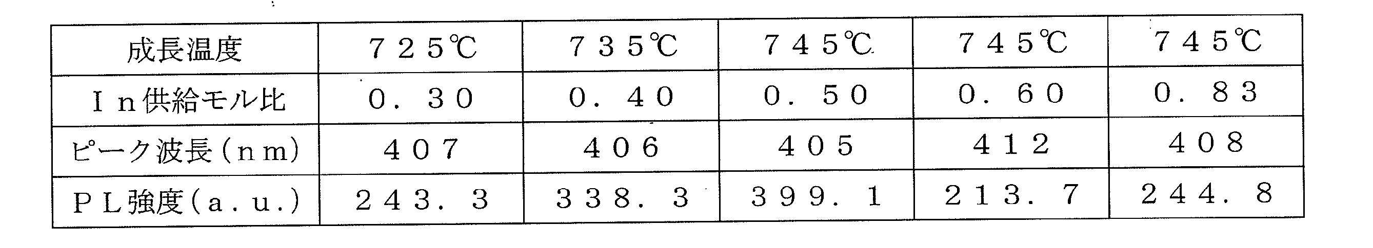
図9は、成長レートを約12.0nm/minに設定した条件の下で得られたIn供給モル比と成長温度との関係を示している。目的の発光波長は、実施形態1における値に等しく、410nm±5nm程度である。In供給モル比が0.50、0.60、0.65、0.70の各々の場合において、発光波長が410nm±5nm程度になるm面In0.1Ga0.9N井戸層14を得るための成長温度は、図9の▲で示されている。▲で示されるIn供給モル比および成長温度で形成したIn0.1Ga0.9N井戸層14の井戸層のPL発光強度は、図9のグラフ中において□で示されている。

図10は、圧力を500Torr、成長レートを約12.0nm/minに設定した条件の下で得られたIn供給モル比と成長温度との関係を示している。目的の発光波長は、実施形態1、2における値に等しく、410nm±5nm程度である。In供給モル比が0.25、0.30、0.40、0.60の各々の場合において、発光波長が410nm±5nm程度になるm面In0.1Ga0.9N井戸層14を得るための成長温度は、図10に▲で示されている。▲で示されるIn供給モル比および成長温度で形成したIn0.1Ga0.9N井戸層14の井戸層のPL発光強度は、図10のグラフ中において□で示されている。

以下、図14を参照しながら、本発明による半導体発光素子を製造する方法の実施形態を説明する。
本実施形態に係る窒化ガリウム系化合物半導体発光素子は、m面から1°以上の角度で傾斜させた面を主面とする窒化ガリウム系化合物半導体層を備えている。この点を除けば、本実施形態の構成は、図14に示される実施形態4の構成と同一である。
11 基板
12 下地となるGaN層
13 GaNバリア層
14 InxGa1-xN(0<x<1)井戸層
15 GaN/InGaN多重量子井戸発光層
101 基板
102 n-GaN層
103 GaNバリア層
104 InxGa1-xN(0<x<1)井戸層
105 GaN/InGaN多重量子井戸発光層
106 p-GaN層
107 n型電極
108 p型電極
Claims (11)
- 主面が非極性面または半極性面である窒化ガリウム系化合物半導体層を有機金属気相成長法によって形成する工程を含む窒化ガリウム系化合物半導体発光素子の製造方法であって、
有機金属気相成長法の成長条件を規定するパラメータは、圧力、成長レート、成長温度、III族原料ガス中に含まれるIn原料ガスの供給モル比であるIn供給モル比を含み、
圧力および成長レートが一定の場合において同一発光波長のInxGa1-xN(0<x<1)層を形成するための成長温度とIn供給モル比との関係を示す曲線上で、成長温度がIn供給モル比の増加に応じて単調に増加する領域と飽和する領域との間の飽和点に対応する成長条件を決定する工程(A)と、
前記成長条件で主面が非極性面または半極性面であるInxGa1-xN(0<x<1)層を成長させる工程(B)と、
を含む窒化ガリウム系化合物半導体発光素子の製造方法。 - 工程(A)は、
有機金属気相成長法により、主面が非極性面または半極性面である複数のInyGa1-yN(0<y<1)層を異なる成長条件で形成する工程(a1)と、
前記複数のInyGa1-yN(0<y<1)層のうちで発光波長が等しいInxGa1-xN(0<x<1)層を形成する成長条件に基づいて、圧力および成長レートが一定の場合における成長温度とIn供給モル比との関係を求める工程(a2)と、
成長温度とIn供給モル比との前記関係を示す曲線上において、成長温度がIn供給モル比の増加に応じて単調に増加する領域と飽和する領域との間の飽和点を決定する工程(a3)と、
を含む、請求項1に記載の窒化ガリウム系化合物半導体発光素子の製造方法。 - 工程(a2)は、圧力および成長レートの異なる組合せの各々について、圧力および成長レートが一定の場合における成長温度とIn供給モル比との関係を求める工程を含む、請求項2に記載の窒化ガリウム系化合物半導体発光素子の製造方法。
- 前記InxGa1-xN(0<x<1)層は、単一量子井戸発光層、または多重量子井戸発光層に含まれる井戸層である、請求項1から3のいずれかに記載の窒化ガリウム系化合物半導体の製造方法。
- 前記井戸層の厚さは2nm以上20nm以下である、請求項4に記載の窒化ガリウム系化合物半導体の製造方法。
- 前記井戸層の厚さは6nm以上16nm以下である、請求項4に記載の窒化ガリウム系化合物半導体の製造方法。
- 工程(B)は、成長圧力を200Torrから600Torrまでの範囲内に調整する工程(b1)を含み、
工程(B)において、調整された前記成長圧力および選択された成長レートについて得られた、成長温度とIn供給モル比との関係を示す曲線上の飽和点に対応する成長温度およびIn供給モル比で、InxGa1-xN(0<x<1)層を成長させる、請求項1から6のいずれかに記載の窒化ガリウム系化合物半導体の製造方法。 - 工程(B)は、成長圧力を常圧に調整する工程(b1)を含み、
工程(B)において、調整された前記成長圧力および選択された成長レートについて得
られた、成長温度とIn供給モル比との関係を示す曲線上の飽和点に対応する成長温度およびIn供給モル比で、InxGa1-xN(0<x<1)層を成長させる、請求項1から6のいずれかに記載の窒化ガリウム系化合物半導体の製造方法。 - 主面が非極性面または半極性面である窒化ガリウム系化合物半導体層を有機金属気相成長法によって成長させる条件を決定する窒化ガリウム系化合物半導体層の成長条件決定方法であって、
有機金属気相成長法の成長条件を規定するパラメータは、圧力、成長レート、成長温度、III族原料ガス中に含まれるIn原料ガスの供給モル比であるIn供給モル比を含み、
有機金属気相成長法により、主面が非極性面または半極性面である複数のInyGa1-yN(0<y<1)層を異なる成長条件で形成する工程(a1)と、
前記複数のInyGa1-yN(0<y<1)層のうちで発光波長が等しいInxGa1-xN(0<x<1)層を形成する成長条件に基づいて、圧力および成長レートが一定の場合における成長温度とIn供給モル比との関係を求める工程(a2)と、
成長温度とIn供給モル比との前記関係を示す曲線上において、成長温度がIn供給モル比の増加に応じて単調に増加する領域と飽和する領域との間の飽和点を決定する工程(a3)と、
を含む、窒化ガリウム系化合物半導体層の成長条件決定方法。 - 工程(a1)および工程(a2)は、
第1のIn供給モル比で第1のInx1Ga1-x1N(0<x1<1)層を形成する工程と、
前記第1のInx1Ga1-x1N(0<x1<1)層を形成するときの成長温度と同一の成長温度において、前記第1のIn供給モル比よりも低い第2のIn供給モル比で第2のInx2Ga1-x2N(0<x2<1)層を形成する工程と、
前記第1のInx1Ga1-x1N(0<x1<1)層を形成するときの成長温度と同一の成長温度において、前記第2のIn供給モル比よりも低い第3のIn供給モル比で第3のInx3Ga1-x3N(0<x3<1)層を形成する工程と、
を含む請求項9に記載の窒化ガリウム系化合物半導体層の成長条件決定方法。 - 工程(a3)では、x2がx1に等しく、かつ、x3がx2とは異なるとき、前記第3のIn供給モル比を、飽和点に相当するIn供給モル比として選択する、請求項10に記載の窒化ガリウム系化合物半導体層の成長条件決定方法。
Priority Applications (3)
| Application Number | Priority Date | Filing Date | Title |
|---|---|---|---|
| JP2011535806A JP4856792B2 (ja) | 2009-11-12 | 2010-10-18 | 窒化物半導体素子の製造方法 |
| CN201080020617XA CN102422391B (zh) | 2009-11-12 | 2010-10-18 | 氮化物半导体元件的制造方法 |
| US13/294,537 US8163573B2 (en) | 2009-11-12 | 2011-11-11 | Method for manufacturing nitride semiconductor element |
Applications Claiming Priority (2)
| Application Number | Priority Date | Filing Date | Title |
|---|---|---|---|
| JP2009258927 | 2009-11-12 | ||
| JP2009-258927 | 2009-11-12 |
Related Child Applications (1)
| Application Number | Title | Priority Date | Filing Date |
|---|---|---|---|
| US13/294,537 Continuation US8163573B2 (en) | 2009-11-12 | 2011-11-11 | Method for manufacturing nitride semiconductor element |
Publications (1)
| Publication Number | Publication Date |
|---|---|
| WO2011058697A1 true WO2011058697A1 (ja) | 2011-05-19 |
Family
ID=43991371
Family Applications (1)
| Application Number | Title | Priority Date | Filing Date |
|---|---|---|---|
| PCT/JP2010/006159 WO2011058697A1 (ja) | 2009-11-12 | 2010-10-18 | 窒化物半導体素子の製造方法 |
Country Status (4)
| Country | Link |
|---|---|
| US (1) | US8163573B2 (ja) |
| JP (1) | JP4856792B2 (ja) |
| CN (1) | CN102422391B (ja) |
| WO (1) | WO2011058697A1 (ja) |
Cited By (2)
| Publication number | Priority date | Publication date | Assignee | Title |
|---|---|---|---|---|
| WO2013042297A1 (ja) * | 2011-09-20 | 2013-03-28 | パナソニック株式会社 | 窒化ガリウム系化合物半導体発光素子及びそれを用いた光源装置 |
| JP2018137400A (ja) * | 2017-02-23 | 2018-08-30 | 大陽日酸株式会社 | 化合物半導体の製造方法 |
Families Citing this family (4)
| Publication number | Priority date | Publication date | Assignee | Title |
|---|---|---|---|---|
| JP2012094688A (ja) * | 2010-10-27 | 2012-05-17 | Sumitomo Electric Ind Ltd | 半導体装置およびその製造方法 |
| JP2015018840A (ja) * | 2013-07-08 | 2015-01-29 | 株式会社東芝 | 半導体発光素子 |
| US11195973B1 (en) * | 2019-05-17 | 2021-12-07 | Facebook Technologies, Llc | III-nitride micro-LEDs on semi-polar oriented GaN |
| US11175447B1 (en) | 2019-08-13 | 2021-11-16 | Facebook Technologies, Llc | Waveguide in-coupling using polarized light emitting diodes |
Citations (2)
| Publication number | Priority date | Publication date | Assignee | Title |
|---|---|---|---|---|
| JPH118407A (ja) * | 1997-06-17 | 1999-01-12 | Toyoda Gosei Co Ltd | 窒化ガリウム系化合物半導体素子の製造方法 |
| JP2007537600A (ja) * | 2004-05-10 | 2007-12-20 | 独立行政法人科学技術振興機構 | 有機金属気相成長法による非極性窒化インジウムガリウム薄膜、ヘテロ構造物およびデバイスの製作 |
Family Cites Families (20)
| Publication number | Priority date | Publication date | Assignee | Title |
|---|---|---|---|---|
| JP3879173B2 (ja) * | 1996-03-25 | 2007-02-07 | 住友電気工業株式会社 | 化合物半導体気相成長方法 |
| JPH10335700A (ja) * | 1997-06-04 | 1998-12-18 | Toshiba Corp | 半導体発光素子およびその製造方法 |
| US6695913B1 (en) * | 1997-07-10 | 2004-02-24 | Sharp Kabushiki Kaisha | III-Nitride optoelectronic semiconductor device containing lattice mismatched III-Nitride semiconductor materials |
| CN1062917C (zh) * | 1998-08-12 | 2001-03-07 | 北京大学 | 铟镓氮单晶薄膜金属有机物气相外延生长技术 |
| JP2001015809A (ja) * | 1999-06-30 | 2001-01-19 | Toshiba Corp | 窒化物系半導体発光素子の製造方法、窒化物系半導体レーザ素子の製造方法、および窒化物系半導体レーザ素子 |
| US6764888B2 (en) * | 2000-09-27 | 2004-07-20 | Sensor Electronic Technology, Inc. | Method of producing nitride-based heterostructure devices |
| US6998281B2 (en) * | 2000-10-12 | 2006-02-14 | General Electric Company | Solid state lighting device with reduced form factor including LED with directional emission and package with microoptics |
| GB2372632A (en) * | 2001-02-23 | 2002-08-28 | Sharp Kk | A method of growing an InGaN semiconductor layer |
| US6955933B2 (en) * | 2001-07-24 | 2005-10-18 | Lumileds Lighting U.S., Llc | Light emitting diodes with graded composition active regions |
| US7208393B2 (en) | 2002-04-15 | 2007-04-24 | The Regents Of The University Of California | Growth of planar reduced dislocation density m-plane gallium nitride by hydride vapor phase epitaxy |
| US6943381B2 (en) * | 2004-01-30 | 2005-09-13 | Lumileds Lighting U.S., Llc | III-nitride light-emitting devices with improved high-current efficiency |
| US7956360B2 (en) | 2004-06-03 | 2011-06-07 | The Regents Of The University Of California | Growth of planar reduced dislocation density M-plane gallium nitride by hydride vapor phase epitaxy |
| US7751455B2 (en) * | 2004-12-14 | 2010-07-06 | Palo Alto Research Center Incorporated | Blue and green laser diodes with gallium nitride or indium gallium nitride cladding laser structure |
| KR101145755B1 (ko) * | 2005-03-10 | 2012-05-16 | 재팬 사이언스 앤드 테크놀로지 에이젼시 | 평면의 반극성 갈륨 질화물의 성장을 위한 기술 |
| TWI377602B (en) * | 2005-05-31 | 2012-11-21 | Japan Science & Tech Agency | Growth of planar non-polar {1-100} m-plane gallium nitride with metalorganic chemical vapor deposition (mocvd) |
| JP4823672B2 (ja) | 2005-12-13 | 2011-11-24 | ローム株式会社 | InGaNの製造方法 |
| KR20080103567A (ko) * | 2006-02-17 | 2008-11-27 | 코넬 리서치 파운데이션 인코포레이티드 | 막 성장 중의 특성 변경 |
| US8021904B2 (en) * | 2007-02-01 | 2011-09-20 | Cree, Inc. | Ohmic contacts to nitrogen polarity GaN |
| US8227791B2 (en) * | 2009-01-23 | 2012-07-24 | Invenlux Limited | Strain balanced light emitting devices |
| CN101560692A (zh) * | 2009-05-13 | 2009-10-21 | 南京大学 | 一种非极性面InN材料的生长方法 |
-
2010
- 2010-10-18 WO PCT/JP2010/006159 patent/WO2011058697A1/ja active Application Filing
- 2010-10-18 JP JP2011535806A patent/JP4856792B2/ja not_active Expired - Fee Related
- 2010-10-18 CN CN201080020617XA patent/CN102422391B/zh not_active Expired - Fee Related
-
2011
- 2011-11-11 US US13/294,537 patent/US8163573B2/en active Active
Patent Citations (2)
| Publication number | Priority date | Publication date | Assignee | Title |
|---|---|---|---|---|
| JPH118407A (ja) * | 1997-06-17 | 1999-01-12 | Toyoda Gosei Co Ltd | 窒化ガリウム系化合物半導体素子の製造方法 |
| JP2007537600A (ja) * | 2004-05-10 | 2007-12-20 | 独立行政法人科学技術振興機構 | 有機金属気相成長法による非極性窒化インジウムガリウム薄膜、ヘテロ構造物およびデバイスの製作 |
Cited By (2)
| Publication number | Priority date | Publication date | Assignee | Title |
|---|---|---|---|---|
| WO2013042297A1 (ja) * | 2011-09-20 | 2013-03-28 | パナソニック株式会社 | 窒化ガリウム系化合物半導体発光素子及びそれを用いた光源装置 |
| JP2018137400A (ja) * | 2017-02-23 | 2018-08-30 | 大陽日酸株式会社 | 化合物半導体の製造方法 |
Also Published As
| Publication number | Publication date |
|---|---|
| US8163573B2 (en) | 2012-04-24 |
| CN102422391A (zh) | 2012-04-18 |
| JPWO2011058697A1 (ja) | 2013-03-28 |
| CN102422391B (zh) | 2013-11-27 |
| JP4856792B2 (ja) | 2012-01-18 |
| US20120058577A1 (en) | 2012-03-08 |
Similar Documents
| Publication | Publication Date | Title |
|---|---|---|
| JP5468709B2 (ja) | 窒化物半導体発光素子、光源及びその製造方法 | |
| US8183071B2 (en) | Method for producing nitride semiconductor optical device and epitaxial wafer | |
| WO2013042297A1 (ja) | 窒化ガリウム系化合物半導体発光素子及びそれを用いた光源装置 | |
| JP4891462B2 (ja) | 窒化ガリウム系化合物半導体発光素子 | |
| JP4952547B2 (ja) | GaN基板、エピタキシャル層付き基板、半導体装置、およびGaN基板の製造方法 | |
| JP2008285364A (ja) | GaN基板、それを用いたエピタキシャル基板及び半導体発光素子 | |
| JP2007254175A (ja) | Iii族窒化物半導体薄膜およびiii族窒化物半導体発光素子 | |
| JP4856792B2 (ja) | 窒化物半導体素子の製造方法 | |
| WO2010113423A1 (ja) | 窒化物半導体の結晶成長方法および半導体装置の製造方法 | |
| JP4647723B2 (ja) | 窒化物半導体の結晶成長方法および半導体装置の製造方法 | |
| JP2008118049A (ja) | GaN系半導体発光素子 | |
| JP6925141B2 (ja) | 半導体基板、半導体発光素子および灯具 | |
| JP5113305B2 (ja) | 窒化ガリウム系化合物半導体発光素子および当該発光素子を備える光源 | |
| JP5388967B2 (ja) | 半導体発光素子 | |
| JP5265404B2 (ja) | 窒化物半導体発光素子およびその製造方法 | |
| JP4960621B2 (ja) | 窒化物半導体成長基板及びその製造方法 | |
| WO2010100689A1 (ja) | 窒化ガリウム系化合物半導体の製造方法、および半導体発光素子 | |
| JP2008118048A (ja) | GaN系半導体発光素子 | |
| WO2020075849A1 (ja) | 半導体成長用基板、半導体素子、半導体発光素子および半導体素子製造方法 | |
| JP7350477B2 (ja) | 半導体成長用基板、半導体素子、半導体発光素子および半導体成長用基板の製造方法 | |
| KR101078062B1 (ko) | 비극성 반도체 소자 및 그것을 제조하는 방법 | |
| JP2019040898A (ja) | 半導体成長用基板、半導体素子、半導体発光素子および半導体素子製造方法 | |
| KR20070071915A (ko) | 질화 갈륨계 화합물 반도체 및 이의 제조 방법 | |
| JP4725436B2 (ja) | Iii族窒化物系化合物半導体の製造方法 | |
| WO2013128893A1 (ja) | 半導体装置の製造方法 |
Legal Events
| Date | Code | Title | Description |
|---|---|---|---|
| WWE | Wipo information: entry into national phase |
Ref document number: 201080020617.X Country of ref document: CN |
|
| 121 | Ep: the epo has been informed by wipo that ep was designated in this application |
Ref document number: 10829665 Country of ref document: EP Kind code of ref document: A1 |
|
| DPE2 | Request for preliminary examination filed before expiration of 19th month from priority date (pct application filed from 20040101) | ||
| ENP | Entry into the national phase |
Ref document number: 2011535806 Country of ref document: JP Kind code of ref document: A |
|
| NENP | Non-entry into the national phase |
Ref country code: DE |
|
| 122 | Ep: pct application non-entry in european phase |
Ref document number: 10829665 Country of ref document: EP Kind code of ref document: A1 |