WO2011042965A1 - 半導体装置および半導体論理回路装置 - Google Patents
半導体装置および半導体論理回路装置 Download PDFInfo
- Publication number
- WO2011042965A1 WO2011042965A1 PCT/JP2009/067499 JP2009067499W WO2011042965A1 WO 2011042965 A1 WO2011042965 A1 WO 2011042965A1 JP 2009067499 W JP2009067499 W JP 2009067499W WO 2011042965 A1 WO2011042965 A1 WO 2011042965A1
- Authority
- WO
- WIPO (PCT)
- Prior art keywords
- region
- gate electrode
- mos transistor
- diffusion
- regions
- Prior art date
- Legal status (The legal status is an assumption and is not a legal conclusion. Google has not performed a legal analysis and makes no representation as to the accuracy of the status listed.)
- Ceased
Links
Images
























Classifications
-
- H—ELECTRICITY
- H10—SEMICONDUCTOR DEVICES; ELECTRIC SOLID-STATE DEVICES NOT OTHERWISE PROVIDED FOR
- H10D—INORGANIC ELECTRIC SEMICONDUCTOR DEVICES
- H10D89/00—Aspects of integrated devices not covered by groups H10D84/00 - H10D88/00
- H10D89/10—Integrated device layouts
-
- H—ELECTRICITY
- H10—SEMICONDUCTOR DEVICES; ELECTRIC SOLID-STATE DEVICES NOT OTHERWISE PROVIDED FOR
- H10D—INORGANIC ELECTRIC SEMICONDUCTOR DEVICES
- H10D84/00—Integrated devices formed in or on semiconductor substrates that comprise only semiconducting layers, e.g. on Si wafers or on GaAs-on-Si wafers
- H10D84/01—Manufacture or treatment
- H10D84/0123—Integrating together multiple components covered by H10D12/00 or H10D30/00, e.g. integrating multiple IGBTs
- H10D84/0126—Integrating together multiple components covered by H10D12/00 or H10D30/00, e.g. integrating multiple IGBTs the components including insulated gates, e.g. IGFETs
- H10D84/0165—Integrating together multiple components covered by H10D12/00 or H10D30/00, e.g. integrating multiple IGBTs the components including insulated gates, e.g. IGFETs the components including complementary IGFETs, e.g. CMOS devices
- H10D84/0188—Manufacturing their isolation regions
-
- H—ELECTRICITY
- H10—SEMICONDUCTOR DEVICES; ELECTRIC SOLID-STATE DEVICES NOT OTHERWISE PROVIDED FOR
- H10D—INORGANIC ELECTRIC SEMICONDUCTOR DEVICES
- H10D84/00—Integrated devices formed in or on semiconductor substrates that comprise only semiconducting layers, e.g. on Si wafers or on GaAs-on-Si wafers
- H10D84/01—Manufacture or treatment
- H10D84/0123—Integrating together multiple components covered by H10D12/00 or H10D30/00, e.g. integrating multiple IGBTs
- H10D84/0126—Integrating together multiple components covered by H10D12/00 or H10D30/00, e.g. integrating multiple IGBTs the components including insulated gates, e.g. IGFETs
- H10D84/0165—Integrating together multiple components covered by H10D12/00 or H10D30/00, e.g. integrating multiple IGBTs the components including insulated gates, e.g. IGFETs the components including complementary IGFETs, e.g. CMOS devices
- H10D84/0191—Manufacturing their doped wells
-
- H—ELECTRICITY
- H10—SEMICONDUCTOR DEVICES; ELECTRIC SOLID-STATE DEVICES NOT OTHERWISE PROVIDED FOR
- H10D—INORGANIC ELECTRIC SEMICONDUCTOR DEVICES
- H10D84/00—Integrated devices formed in or on semiconductor substrates that comprise only semiconducting layers, e.g. on Si wafers or on GaAs-on-Si wafers
- H10D84/01—Manufacture or treatment
- H10D84/02—Manufacture or treatment characterised by using material-based technologies
- H10D84/03—Manufacture or treatment characterised by using material-based technologies using Group IV technology, e.g. silicon technology or silicon-carbide [SiC] technology
- H10D84/038—Manufacture or treatment characterised by using material-based technologies using Group IV technology, e.g. silicon technology or silicon-carbide [SiC] technology using silicon technology, e.g. SiGe
-
- H—ELECTRICITY
- H10—SEMICONDUCTOR DEVICES; ELECTRIC SOLID-STATE DEVICES NOT OTHERWISE PROVIDED FOR
- H10D—INORGANIC ELECTRIC SEMICONDUCTOR DEVICES
- H10D84/00—Integrated devices formed in or on semiconductor substrates that comprise only semiconducting layers, e.g. on Si wafers or on GaAs-on-Si wafers
- H10D84/80—Integrated devices formed in or on semiconductor substrates that comprise only semiconducting layers, e.g. on Si wafers or on GaAs-on-Si wafers characterised by the integration of at least one component covered by groups H10D12/00 or H10D30/00, e.g. integration of IGFETs
- H10D84/82—Integrated devices formed in or on semiconductor substrates that comprise only semiconducting layers, e.g. on Si wafers or on GaAs-on-Si wafers characterised by the integration of at least one component covered by groups H10D12/00 or H10D30/00, e.g. integration of IGFETs of only field-effect components
- H10D84/83—Integrated devices formed in or on semiconductor substrates that comprise only semiconducting layers, e.g. on Si wafers or on GaAs-on-Si wafers characterised by the integration of at least one component covered by groups H10D12/00 or H10D30/00, e.g. integration of IGFETs of only field-effect components of only insulated-gate FETs [IGFET]
- H10D84/85—Complementary IGFETs, e.g. CMOS
-
- H—ELECTRICITY
- H10—SEMICONDUCTOR DEVICES; ELECTRIC SOLID-STATE DEVICES NOT OTHERWISE PROVIDED FOR
- H10D—INORGANIC ELECTRIC SEMICONDUCTOR DEVICES
- H10D84/00—Integrated devices formed in or on semiconductor substrates that comprise only semiconducting layers, e.g. on Si wafers or on GaAs-on-Si wafers
- H10D84/01—Manufacture or treatment
- H10D84/0123—Integrating together multiple components covered by H10D12/00 or H10D30/00, e.g. integrating multiple IGBTs
- H10D84/0126—Integrating together multiple components covered by H10D12/00 or H10D30/00, e.g. integrating multiple IGBTs the components including insulated gates, e.g. IGFETs
- H10D84/0165—Integrating together multiple components covered by H10D12/00 or H10D30/00, e.g. integrating multiple IGBTs the components including insulated gates, e.g. IGFETs the components including complementary IGFETs, e.g. CMOS devices
- H10D84/0167—Manufacturing their channels
Definitions
- the present invention generally relates to a semiconductor device, and more particularly to a semiconductor device using a dynamic threshold MOS transistor (hereinafter referred to as a Dt-MOS transistor) and a semiconductor logic circuit device using a Dt-MOS transistor.
- a Dt-MOS transistor dynamic threshold MOS transistor
- a gate electrode is short-circuited to a semiconductor layer or well region in which a channel region is formed, and an input signal is applied simultaneously to the semiconductor layer or well region in which the gate electrode and the channel region are formed.
- the MOS transistor is capable of realizing a low off-state current and a large on-state current with a low threshold, and is suitable for low power consumption operation with a low power supply voltage.
- a semiconductor layer or well region in which a channel region is formed may be referred to as a body.
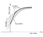
- FIG. 1 is a diagram for explaining the principle of a general Dt-MOS transistor
- FIG. 2 is a graph showing the operating characteristics of the Dt-MOS transistor 10 of FIG.
- a Dt-MOS transistor 10 is an n-channel MOS transistor on a silicon substrate 11 on which a p-type well 11P including an n-type doped source region 11S and a drain region 11D is formed.
- a gate electrode 13 made of, for example, n-type polysilicon is formed on a channel region 11C between the source region 11S and the drain region 11D via a gate insulating film 12. Is formed.
- the gate electrode 13 is further electrically connected to the p-type well 11P, that is, the body, and the signal voltage applied to the gate electrode 13 is also applied to the body 11P. Is done.
- the signal voltage acts to lower the threshold voltage of the Dt-MOS transistor 10
- the operating characteristic of the Dt-MOS transistor 10 is that of the MOS transistor having a low threshold voltage as the signal voltage increases. Asymptotically. Therefore, the Dt-MOS transistor 10 is switched on with a low signal voltage.
- the Dt-MOS transistor 10 when the signal voltage is 0V or a low voltage in the vicinity thereof, the potential of the body 11P is 0V or in the vicinity thereof, and the operating characteristics of the Dt-MOS transistor 10 are the operating characteristics of the MOS transistor having a high threshold voltage. Asymptotically. That is, the threshold voltage of the Dt-MOS transistor 10 is not different from that of a normal n-channel MOS transistor having a high threshold voltage. As a result, the Dt-MOS transistor 10 has a low off-current or leakage as shown in FIG. The switch-off operation characterized by current is shown.
- a Dt-MOS transistor When such a Dt-MOS transistor is formed on a normal silicon substrate (hereinafter referred to as a silicon bulk substrate) cut from a single crystal silicon ingot, the leakage current of the source and drain increases. In addition, there is a problem that the junction capacitance increases between the source region or drain region and the body, and the operation speed of the Dt-MOS transistor decreases due to the influence of the time constant. For this reason, conventionally, a Dt-MOS transistor is generally formed on an SOI substrate (Non-patent Document 1). The characteristics shown in FIG. 2 are for the Dt-MOSS transistor described on Non-Patent Document 2 and formed on such an SOI substrate.
- a dynamic threshold like a Dt-MOS transistor is formed on the same substrate.
- various other transistors need to be integrated, and some of them may include input / output transistors that do not want to perform a dynamic threshold operation, analog transistors, and the like.
- the Dt-MOS transistor is formed on the SOI substrate, the film thickness of the silicon film 11P constituting the body is reduced, which increases the resistance of the body, and the operation speed of the transistor due to the effect of the time constant. There arises a problem of reduction.
- Non-Patent Document 2 a source region and a drain region are formed as an elevated source / drain structure on an element isolation structure to avoid an increase in the element area, and between the source region or the drain region and the body. A configuration for reducing the junction capacitance is proposed.
- this conventional structure solves the problems of increased source leakage current and increased junction capacitance, the current path between the body and the source or drain region is narrowed, resulting in increased source resistance.
- the gate electrode is formed so as to face the source region or the drain region through the insulating film, there is a problem that the parasitic capacitance between the gate electrode and the source region or the drain region increases. The manufacturing process is complicated.
- a semiconductor device is formed in a silicon bulk substrate having an element region defined by an element isolation region, a first dynamic threshold MOS transistor formed in the element region, and the element region.
- a second dynamic threshold MOS transistor wherein the element region comprises a well having a first conductivity type, and the first dynamic threshold MOS transistor has a first gate on the surface of the silicon bulk substrate.
- a first gate electrode formed through an insulating film; a first diffusion region formed on a first side of the first gate electrode in the well; and the first gate electrode with respect to the first gate electrode.
- the S transistor includes a second gate electrode formed on a surface of the silicon bulk substrate on the second side of the first gate electrode via a second gate insulating film, the well, A third diffusion region formed on the first gate electrode side with respect to the second gate electrode, and a fourth diffusion region formed on the opposite side of the third diffusion region with respect to the second gate electrode.
- the first and second gate electrodes and the first to fourth diffusion regions have a second conductivity type opposite to that of the well, and the second diffusion region
- the third diffusion region is composed of the same diffusion region formed in the well, and the first to fourth diffusion regions are in contact with the lower ends of the first to fourth diffusion regions.
- a fourth insulating region is formed, and the second insulating region and the third insulating region are formed.
- the edge region is composed of the same insulating region, and the first dynamic threshold MOS is provided between the first insulating region and the second insulating region along the first gate electrode.
- a first body region of the first conductivity type that constitutes a body of the transistor extends as a part of the element region, and is between the third insulating region and the fourth insulating region.
- the second body region of the first conductivity type constituting the body of the second dynamic threshold MOS transistor extends as a part of the element region along the second gate electrode.
- the first gate electrode is connected to the first region, the second gate electrode is connected to the second region, and the lower ends of the first to fourth insulating regions are The first and second bodies;
- the lower end of the region is set deeper than the lower end of the region, and the lower ends of the first and second body regions are set deeper than the lower ends of the first to fourth diffusion regions.
- the insulating region is located immediately below the diffusion region serving as the source or drain of each Dt-MOS transistor, and the diffusion region corresponding to each insulating region.
- the junction capacitance associated with these diffusion regions is reduced, and the junction leakage current is reduced.
- the element area can be reduced by sharing the diffusion region of one Dt-MOS transistor with the diffusion region of the other Dt-MOS transistor. .
- the body regions of these two Dt-MOS transistors can be electrically independent. Further, by forming the lower ends of these body regions deeper than the lower ends of the respective diffusion regions, it is possible to suppress a short circuit between the diffusion regions and the wells constituting the element regions.
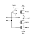
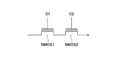
- FIG. 1 is an equivalent circuit diagram of a semiconductor logic circuit device according to a first embodiment.
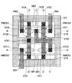
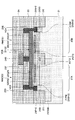
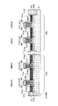
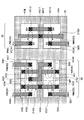
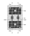
- FIG. 4 is a plan view showing a layout of the semiconductor logic circuit device of FIG. 3.
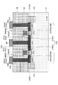
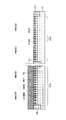
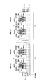
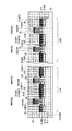
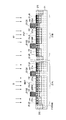
- FIG. 5 is a cross-sectional view taken along line AA ′ in FIG.
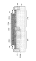
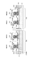
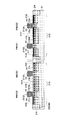
- FIG. 5 is a sectional view taken along line BB ′ in FIG.
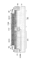
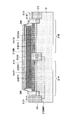
- FIG. 5 is a cross-sectional view taken along line CC ′ in FIG.
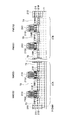
- FIG. 5 is a sectional view taken along line DD ′ in FIG.
- FIG. 5 is a sectional view taken along line EE ′ in FIG.
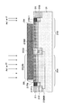
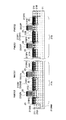
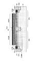
- FIG. 5 is a sectional view (No. 1) showing a manufacturing process of the semiconductor logic circuit device of FIG. 4;
- FIG. 5 is a sectional view (No. 2) showing a manufacturing process of the semiconductor logic circuit device of FIG. 4;
- FIG. 6 is a sectional view (No. 3) showing a manufacturing step of the semiconductor logic circuit device of FIG. 4;
- FIG. 6 is a sectional view (No. 4) showing a manufacturing step of the semiconductor logic circuit device of FIG. 4;
- FIG. 6 is a sectional view (No. 5) showing a manufacturing step of the semiconductor logic circuit device of FIG. 4;
- FIG. 6 is a sectional view (No. 6) showing a manufacturing step of the semiconductor logic circuit device of FIG. 4;
- FIG. 7 is a sectional view (No.).
- FIG. 9 is a sectional view (No. 8) showing a manufacturing step of the semiconductor logic circuit device of FIG. 4;
- FIG. 9 is a sectional view (No. 9) showing a manufacturing step of the semiconductor logic circuit device of FIG. 4;
- FIG. 10 is a sectional view (No. 10) showing a manufacturing step of the semiconductor logic circuit device of FIG. 4;
- FIG. 11 is a sectional view (No. 11) showing a manufacturing step of the semiconductor logic circuit device of FIG. 4;
- FIG. 13 is a sectional view (No. 12) showing a manufacturing step of the semiconductor logic circuit device of FIG. 4;
- FIG. 13 is a sectional view (No.
- FIG. 15 is a sectional view (No. 14) showing a manufacturing step of the semiconductor logic circuit device of FIG. 4;
- FIG. 15 is a sectional view (No. 15) showing a manufacturing step of the semiconductor logic circuit device of FIG. 4;
- FIG. 17 is a cross-sectional view (No. 16) showing a manufacturing step of the semiconductor logic circuit device of FIG. 4;
- FIG. 17 is a sectional view (No. 17) showing a manufacturing step of the semiconductor logic circuit device of FIG. 4;
- FIG. 19 is a sectional view (No. 18) showing a manufacturing step of the semiconductor logic circuit device of FIG. 4;
- FIG. 19 is a sectional view (No.).
- FIG. 10A is a diagram (part 1) for explaining the ion implantation process of FIGS. 10O to 10R; FIG.
- FIG. 10D is a diagram (part 2) illustrating the ion implantation process of FIGS. 10O to 10R.
- FIG. 10D is a diagram (No. 3) for explaining the ion implantation step in FIGS. 10O to 10R;
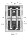
- FIG. 10D is a diagram (part 4) for explaining the ion implantation step of FIGS. 10O to 10R; It is a figure which shows one modification of 1st Embodiment. It is a top view which shows the other modification of 1st Embodiment.
- FIG. 13B is a sectional view taken along line XX ′ in FIG. 13B. It is a top view which shows another modification of 1st Embodiment.
- FIG. 10D is a diagram (part 2) illustrating the ion implantation process of FIGS. 10O to 10R.
- FIG. 10D is a diagram (No. 3) for explaining the ion implantation step in FIGS. 10O to 10R;
- FIG. 10D is
- FIG. 13B is a cross-sectional view taken along line YY ′ in FIG. 13B. It is a top view which shows another modification of 1st Embodiment.
- FIG. 6A is a sectional view (No. 1) showing a manufacturing process of the semiconductor logic circuit of FIG. 4 according to the second embodiment.
- FIG. 5D is a cross-sectional view (part 2) illustrating the manufacturing process of the semiconductor logic circuit of FIG. 4 according to the second embodiment.
- FIG. 5D is a cross-sectional view (part 3) illustrating the manufacturing process of the semiconductor logic circuit of FIG. 4 according to the second embodiment.
- FIG. 6A is a diagram (part 1) illustrating a manufacturing process of the semiconductor logic circuit of FIG. 4 according to the third embodiment; FIG.
- FIG. 6A is a diagram (part 2) illustrating a manufacturing process of the semiconductor logic circuit of FIG.
- FIG. 10 is a diagram (part 3) illustrating a manufacturing process of the semiconductor logic circuit of FIG. 4 according to the third embodiment
- FIG. 6A is a diagram (part 4) illustrating a manufacturing process of the semiconductor logic circuit of FIG. 4 according to the third embodiment
- It is a top view which shows the layout of the semiconductor logic integrated circuit device by 4th Embodiment.
- FIG. 10 is an equivalent circuit diagram showing a transfer gate according to a fifth embodiment.
- FIG. 3 shows an equivalent circuit diagram of the semiconductor logic circuit device 20 according to the first embodiment
- FIG. 4 is a plan view showing the layout thereof.
- 5 to 9 are sectional views taken along lines AA ′, BB ′, CC ′, DD ′, and EE ′ in FIG. 4, respectively.
- the semiconductor logic circuit device 20 is a two-input NAND device, which includes two p-channel MOS transistors PMOS1 and PMOS2 connected in parallel and two serially connected devices.
- the n-channel MOS transistors NOS1 and NMOS2 are configured.
- the p-channel MOS transistors PMOS1 and PMOS2 and the n-channel MOS transistors NMOS1 and NMOS2 are p - type doped silicon bulk substrate 21 (FIG. 5 to FIG. 5). (See FIG. 9).
- the source S of the p-channel MOS transistors PMOS1 and PMOS2 which is the parallel connection is connected to the power supply V CC to the common, the drain D of the p-channel MOS transistors PMOS1 and PMOS2 are common, drains D of the n-channel MOS transistor NMOS1 Connected to.
- the source S of the n-channel MOS transistor NMOS1 is connected to the drain D of the n-channel MOS transistor NMOS2, and the source S of the n-channel MOS transistor NMOS2 is connected to the ground power supply GND.
- a first input signal IN1 is supplied to the gate electrodes of the p-channel MOS transistor PMOS2 and the n-channel MOS transistor NMOS1, and the gate electrodes of the p-channel MOS transistor PMOS1 and the n-channel MOS transistor NMOS2 are supplied to the gate electrodes. Is supplied with the second input signal IN1, and a logic output signal is obtained at the connection node N between the drains D of the p-channel MOS transistors PMOS1 and PMOS2 and the drain D of the n-channel MOS transistor NMOS1.
- a first element region 21A and a second element region 21B are defined in the silicon bulk substrate 21 by an element isolation region 21I having an STI structure.
- the n-channel MOS transistor NMOS1 is formed using the polysilicon pattern 21G1 as a gate electrode
- the n-channel MOS transistor NMOS2 is formed using the polysilicon pattern 21G2 as a gate electrode.
- the polysilicon patterns 21G1 and 21G2 further extend to the element region 21B.
- the polysilicon pattern 21G1 and the polysilicon pattern 21G2 are used as the gate electrodes, respectively.
- MOS transistors PMOS2 and PMOS1 are formed.
- the polysilicon pattern 21G1 is electrically connected to the element regions 21A and 21B at the via contacts VC1 and VC2, respectively.
- the polysilicon pattern 21G2 is electrically connected to the element regions at the via contacts VC3 and VC4, respectively. It is electrically connected to 21A and 21B.
- the n-channel MOS transistors NMOS1 and NMOS2 and the p-channel MOS transistors PMOS1 and PMOS2 all exhibit the dynamic threshold operation as described above with reference to FIG.
- the p-channel MOS transistor PMOS1 shares its drain with the drain of the p-channel MOS transistor PMOS2, and the n-channel MOS transistor NMOS1 shares its source with the drain of the n-channel MOS transistor NMOS2.
- the p-channel MOS transistors PMOS1 and PMOS2 and the n-channel MOS transistors NMOS1 and NMOS2 are formed in the element regions of the semiconductor logic circuit device 20 as compared with the case where the element regions are separated by the element isolation structure. The area can be greatly reduced.
- a via contact VC5 to which the input signal A is supplied is formed on the element isolation region 21I between the element regions 21A and 21B, though not visible in the plan view of FIG. (See FIG. 7).
- a via contact VC6 to which the input signal B is supplied is formed in the polysilicon pattern 21G2 on the element isolation region 21I between the element regions 21A and 21B.
- each of the source region S of the p-channel MOS transistors PMOS1 and PMOS 2 each of the power pattern - supplying the power supply voltage V CC from the emission PW1 and PW2 Via contacts VC7 and VC8 are formed, and the drain D of the p-channel MOS transistors PMOS1 and PMOS2 connected in common is connected to the via contact VC10 provided in the drain D of the n-channel MOS transistor NMOS1. They are connected via the VC 9 and the wiring pattern WP.
- the source region of the n-channel MOS transistor NMOS2 is connected to GND via a via contact VC11 and a ground pattern GD1, and the output of the semiconductor logic circuit 20 is obtained on the wiring pattern WP. It is done.
- the element region 21A is formed with an insulating pattern SB1 that separates the via contacts VC1 and VC3 from each other and also from the via contacts VC10 and VC11.
- the insulating pattern SB1 functions as a silicide block structure.
- a silicide layer (not shown) is formed in the element region 21A, a short circuit between the via contact VC1 and the via contacts VC3, VC10, VC11 is avoided. Is done.
- a silicide layer (not shown) is formed in the element region 21A as a result of forming the insulating pattern SB1, a short circuit between the via contact VC3 and the via contacts VC1, VC10, VC11 is avoided.
- an insulating pattern SB2 that separates the via contacts VC2 and VC4 from each other and also separates from the via contacts VC7 and VC8 is formed.
- the insulating pattern SB2 also functions as a silicide block structure. As a result, even when a silicide layer (not shown) is formed in the element region 21B, a short circuit between the via contact VC2 and the via contacts VC4, VC7, VC8 is avoided. Is done.
- the insulating patterns SB1 and SB2 can be formed by adding a mask process when forming sidewall insulating films on the polysilicon patterns 21G1 and 21G2.
- FIG. 5 is a sectional view taken along line AA ′ in the plan view of FIG.
- a deep n-type well 21DNW is formed in the element region 21A, and an n-type doped gate composed of the polysilicon pattern 21G1 is formed on the surface portion of the n-type well 21DNW.
- a p-type well 21PW is formed.
- the surface portions of the p-type bodies 21BY1 and 21BY2 correspond to the channel region CH1 of the MOS transistor NMOS1 immediately below the gate electrode 23G1N and the channel region CH2 of the MOS transistor NMOS2 immediately below the gate electrode 23G2N, respectively.
- P-type channel doped regions 21NVT1 and 21NVT2 for threshold control are formed as part of p-type implantation region 21NVT, respectively.
- the p-type channel dope regions 21NVT1 and 21NVT2 can be shared by the p-type well 21PW constituting the bodies 21BY1 and 21BY2.
- the polysilicon pattern 21G1 constituting the gate electrode 23G1N is electrically connected to the body 21BY1 at the via contact VC1.
- the gate electrode 23G1N is also connected to the body 21BY1.
- the n-channel MOS transistor NMOS1 performs a dynamic threshold operation.
- the polysilicon pattern 21G2 constituting the gate electrode 23G2N is electrically connected to the body 21BY2 at the via contact VC3.
- the input applied to the gate electrode 23G2N is also applied to the body 21BY2.
- the signal IN2 is applied simultaneously, and the n-channel MOS transistor NMOS2 performs a dynamic threshold operation as described above with reference to FIG.
- the gate electrodes 21G1N and 21G2N are formed on the silicon bulk substrate 21 via gate insulating films 22Ox1 and 22Ox2, respectively.
- the gate electrodes 21G1N and 21G2N are formed on the first side of the channel region CH1.
- An n-type diffusion region 21DN1 serving as the drain of the n-channel MOS transistor NMOS1 is disposed on the side facing the n-type diffusion region 21DN1 across the channel region CH1, and an n-type diffusion serving as the source of the n-channel MOS transistor NMOS1.
- Region 21SN1 is formed.
- an n-type diffusion region 21DN2 serving as a drain of the n-channel MOS transistor NMOS2 is formed on the first side of the channel region CH2, and the n-type diffusion region is sandwiched between the channel region CH2.
- An n-type diffusion region 21SN2 serving as the source of the n-channel MOS transistor NMOS2 is formed on the side facing 21DN2.
- the n-type diffusion region 21SN1 and the n-type diffusion region 21DN2 are actually composed of the same n-type diffusion region, so that in the present embodiment, as described above, the semiconductor logic circuit It is possible to reduce the occupied area of 20.
- the insulating region 21I1 is continuous with the adjacent element isolation region 21I
- the insulating region 21I3 is continuous with the adjacent element isolation region 21I
- the insulating regions 21I1, 21I2, and 21I3 have lower ends. It is formed to be deeper than the lower end of the shallow p-type well 21PW constituting the bodies 21BY1 and 21BY2. As a result, the bodies 21BY1 and 21BY2 are electrically separated from each other, and the problem that the input signals IN1 and IN2 interfere with each other does not occur.
- the lower ends of the n-type diffusion regions 21DN1, 21SN1, and thus 21DN2 and 21SN2, are formed shallower than the lower end of the shallow p-type well 21PW, and these n-type diffusion regions are formed below the n-type well 21NW. There is no risk of short circuit.
- interlayer insulating films 23 and 24 are stacked on the silicon bulk substrate 21, and the via contact VC 10 contacts the diffusion region 21 DN 1 through the interlayer insulating films 23 and 24. Yes.
- the via contact VC11 is in contact with the diffusion region 21SN2 through the interlayer insulating films 23 and 24.
- the via contact VC10 is in contact with a wiring pattern WP formed on the interlayer insulating film 24, and the via contact VC11 is formed on the interlayer insulating film 24 and connected to the ground power supply GND.
- the wiring pattern GD1 is connected.
- FIG. 6 is a sectional view taken along line BB ′ in the plan view of FIG.
- Shallow n-type wells 21NW constituting the respective bodies 21BY4 and 21BY3 of the p-channel MOS transistors PMOS2 and PMOS1 are respectively formed immediately below the type-doped gate electrode 21G1P.
- the surface portions of the n-type bodies 21BY3 and 21BY4 correspond to the channel region CH3 of the MOS transistor PMOS1 immediately below the gate electrode 23G1P and the channel region CH4 of the MOS transistor PMOS2 immediately below the gate electrode 23G1P, respectively.
- N-type channel doped regions 21PVT1 and 21PVT2 for threshold control are formed as part of the n-type implantation region PVT, respectively.
- the n-type channel dope regions 21PVT1 and 21PVT2 can be shared by the n-type well 21NW constituting the bodies 21BY3 and 21BY4.
- the polysilicon pattern 21G1 constituting the gate electrode 23G2P is electrically connected to the body 21BY4 at the via contact VC2, and as a result, the gate electrode 23G2P is also connected to the body 21BY4.
- the input signal IN1 applied to is simultaneously applied, and the p-channel MOS transistor PMOS2 performs a dynamic threshold operation.
- the polysilicon pattern 21G2 constituting the gate electrode 23G1P is electrically connected to the body 21BY3 at the via contact VC4.
- the input applied to the gate electrode 23G1P is also applied to the body 21BY3.
- the signal IN2 is applied simultaneously, and the p-channel MOS transistor PMOS1 performs the dynamic threshold operation as described above with reference to FIG.
- the gate electrodes 21G2P and 21G1P are formed on the silicon bulk substrate 21 via gate insulating films 22Ox3 and 22Ox4, respectively.
- a first region of the channel region CH4 is formed in the p-type silicon bulk substrate 21, a first region of the channel region CH4 is formed.
- the p-type diffusion region 21SP2 serving as the drain of the p-channel MOS transistor PMOS2 is disposed on the side, and the source of the p-channel MOS transistor PMOS2 is disposed on the side facing the p-type diffusion region 21SP2 across the channel region CH4.
- a p-type diffusion region 21DP2 is formed.
- a p-type diffusion region 21DP1 serving as the drain of the p-channel MOS transistor PMOS1 is formed on the first side of the channel region CH3, and the p-type diffusion region 21DP1 is sandwiched between the channel region CH3 and the p-type diffusion region 21DP1.
- an n type diffusion region 21SP1 serving as the source of the p-channel MOS transistor NMOS1 is formed on the side facing the type diffusion region 21DP1.
- the p-type diffusion region 21DP2 and the p-type diffusion region 21DP1 are actually composed of the same p-type diffusion region, and are formed by being electrically connected to the via contact VP9 in FIG. Has been.
- the occupation area of the semiconductor logic circuit 20 is reduced. It is possible to reduce.
- the via contact VP9 extends through the interlayer insulating films 23 and 24 and is connected to a wiring pattern WP formed on the interlayer insulating film 24.
- insulating regions 21I4, 21I5 and 21I6 made of silicon oxide films are provided immediately below the p-type diffusion region 21SP1, the p-type diffusion region 21DP1, that is, the p-type diffusion region 21DP2, and the p-type diffusion region 21SP2. Note that each is formed.
- the insulating region 21I4 is continuous to the adjacent element isolation region 21I
- the insulating region 21I6 is also continuous to the adjacent element isolation region 21I
- the lower ends of the insulating regions 21I3, 21I4 and 21I5 are It is formed so as to be deeper than the lower end of shallow n-type well 21NW constituting bodies 21BY3 and 21BY4.
- the bodies 21BY3 and 21BY4 are electrically separated from each other, and the problem that the input signals IN1 and IN2 interfere with each other does not occur.
- the lower ends of the p-type diffusion regions 21SP1, 21DP1, and thus 21DP2 and 21SP2 are formed shallower than the lower end of the shallow well 21NW, and these p-type diffusion regions are formed under the p-type silicon bulk substrate 21 below. There is no risk of short circuit.
- the via contact VC1 is in contact with the diffusion region 21SP2 through the interlayer insulating films 23 and 24.
- the via contact VC8 is in contact with the diffusion region 21SP1 through the interlayer insulating films 23 and 24.
- a power supply wiring pattern PW1 formed on the interlayer insulating film 24 is in contact with the via contact VC7, and a power supply wiring pattern PW2 is connected to the via contact VC8 on the interlayer insulating film 24.
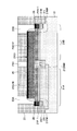
- FIG. 7 is a sectional view of the semiconductor logic circuit device 20 taken along the line CC ′ in FIG.
- a shallow p-type well 21PW including the channel dope region NVT1 is formed immediately below the gate electrode 23G1N constituted by a part of the polysilicon pattern 21G1.
- the shallow p-type well 21PW has a high concentration for ohmic connection corresponding to an end portion of the polysilicon pattern 21G1 constituting the gate electrode 23G1N in the element region 21A.
- P-type region 21P + is formed.
- an opening 23A exposing the end of the p-type region 21P + and the gate electrode 23G1N is formed in the interlayer insulating film 23, and the opening 23A is filled with a via contact VC1 made of a metal plug.
- the gate electrode 23G1N is electrically connected to the shallow well 21PW.
- a shallow n-type well 21NW including the channel dope region PVT2 is formed immediately below the gate electrode 23G2P constituted by a part of the polysilicon pattern 21G1, and the shallow n
- the type well 21NW includes a high-concentration n + type ohmic region for ohmic connection corresponding to an end portion of the polysilicon pattern 21G1 in the element region 21B constituting the gate electrode 23G2P. 21N + 1 is formed.
- the interlayer insulating film 23 is formed with an opening 23B exposing the end of the n + type ohmic region 21N + 1 and the gate electrode 23G2P, and the opening 23B is filled with a via contact VC2 made of a metal plug.
- the gate electrode 23G2P is electrically connected to the shallow well 21NW through the n + type ohmic region 21N + 1.
- the p-channel MOS transistor PMOS1 and the n-channel MOS transistor NMOS2 each perform a dynamic threshold operation.
- a contact hole 23C is formed in the interlayer insulating film 23 corresponding to the element isolation region 21I between the element region 21A and the element region 21B.
- a via contact VC5 made of a plug By filling with a via contact VC5 made of a plug, a signal wiring pattern 24A formed on the interlayer insulating film 23 and supplied with a signal IN1 is electrically connected to the polysilicon pattern 21G1.
- a low-resistance silicide layer is formed on the polysilicon pattern 21G1, and therefore, in the polysilicon pattern 21G1, the n-type doped gate electrode 23G1N and There is no problem that the electric resistance increases at the joint with the gate electrode 23G1P doped in p-type.
- the via contact CV5 is not shown in the plan view of FIG. 4 because it is formed immediately below the wiring pattern WP formed on the interlayer insulating film 24.
- FIG. 8 is a cross-sectional view of the semiconductor logic circuit device 20 taken along line DD ′ in FIG.
- the shallow p-type well 21PW is formed including the channel dope region NVT2 immediately below the gate electrode 23G2N constituted by a part of the polysilicon pattern 21G2.
- the shallow p-type well 21PW is connected to the polysilicon pattern 21G2 for ohmic connection corresponding to the end of the portion constituting the gate electrode 23G2N in the element region 21A.
- a high concentration p-type region 21P + 2 is formed.
- an opening 23A exposing the end of the p-type ohmic region 21P + 2 and the gate electrode 23G2N is formed in the interlayer insulating film 23, and the opening 23A is filled with a via contact VC3 made of a metal plug.
- the gate electrode 23G2N is electrically connected to the shallow well 21PW through the p-type ohmic region 21P2.
- a shallow n-type well 21NW including the channel dope region PVT2 is formed immediately below the gate electrode 23G1P constituted by a part of the polysilicon pattern 21G2, and the shallow n-type well 21NW is formed.
- an opening 23E exposing the end of the n-type ohmic region 21N + 2 and the gate electrode 23G1P is formed in the interlayer insulating film 23, and the opening 23E is filled with a via contact VC4 made of a metal plug.
- the gate electrode 23G1P is electrically connected to the shallow well 21NW via the n-type ohmic region 21N + 2.
- the p-channel MOS transistor PMOS1 and the n-channel MOS transistor NMOS2 each perform a dynamic threshold operation.
- a contact hole 23F is formed in the interlayer insulating film 23 corresponding to the element isolation region 21I between the element region 21A and the element region 21B.
- the signal wiring pattern 24B formed on the interlayer insulating film 23 and supplied with the signal IN2 is electrically connected to the polysilicon pattern 21G2.
- a low-resistance silicide layer is also formed on the polysilicon pattern 21G2. Therefore, in the polysilicon pattern 21G2, the n-type doped gate electrode 23G2N and There is no problem that the electrical resistance increases at the joint with the gate electrode 23G2P doped in p-type.
- FIG. 9 is a cross-sectional view taken along line EE ′ in the plan view of FIG.
- the wiring pattern WP extends over the interlayer insulating film 24 across the via contact VC5 and the signal wiring pattern 24A formed on the polysilicon pattern 21G1. It can be seen that the via contact VC9 contacts the p-type diffusion region 21DP1, that is, 21DP2, and the via contact CV10 contacts the n-type diffusion region 21DN1.
- the gate electrode 23G1N of the n-channel MOS transistor NMOS1 shown in FIG. 5 is formed of a p-type well 21PW and extends directly under the channel region 21CH1, as shown in FIG. Are electrically connected to each other by a via contact VC1 and a p-type ohmic region 21P + 1. Therefore, the n-channel MOS transistor NMOS1 operates at a low voltage and exhibits low dynamic threshold operation as described in FIG.
- the Dt-MOS transistor is characterized by an off current and a large on current.
- the gate electrode 23G2N of the n-channel MOS transistor NMOS2 shown in FIG. 5 is formed in a body 21BY2 which is made of a p-type well 21PW and extends immediately below the channel region 21CH2, as shown in FIG.
- the n-channel MOS transistor NMOS2 is also electrically connected by the via contact VC3 and the p-type ohmic region 21P + 2, so that the n-channel MOS transistor NMOS2 also operates at a low voltage and exhibits a dynamic threshold operation as described in FIG.
- the Dt-MOS transistor is characterized by a low off current and a large on current.
- the gate electrode 23G1P of the p-channel MOS transistor PMOS1 shown in FIG. 6 has an n-type well 21NW and extends directly under the channel region 21CH3, as shown in FIG. Are electrically connected to each other by a via contact VC4 and an n-type ohmic region 21N + 2.
- the p-channel MOS transistor PMOS1 performs the dynamic threshold operation as described with reference to FIG.
- the resulting Dt-MOS transistor is characterized by current and large on-current.
- the gate electrode 23G2P of the p-channel MOS transistor PMOS2 shown in FIG. are electrically connected to each other by a via contact VC2 and an n + type ohmic region 21N + 1. Therefore, the p-channel MOS transistor PMOS2 operates at a low voltage and exhibits low dynamic threshold operation as described with reference to FIG.
- the Dt-MOS transistor is characterized by an off current and a large on current.
- insulating regions 21I2 and 21I1 made of silicon oxide films are formed immediately below the n-type diffusion region 21SN1 constituting the source region and the n-type diffusion region 21DN1 constituting the drain region, respectively. Therefore, the junction capacitance associated with these diffusion regions is reduced, the operation speed is improved, and the junction leakage current is reduced.
- insulating regions 21I3 and 21I2 made of silicon oxide films are formed immediately below the n-type diffusion region 21SN2 constituting the source region and the n-type diffusion region 21DN2 constituting the drain region, respectively. Therefore, the junction capacitance associated with these diffusion regions is reduced, the operation speed is improved, and the junction leakage current is reduced.
- the body 21By1 and the body 21BY2 are electrically connected.
- the input signal In1 and the input signal IN2 do not interfere with each other.
- the lower ends of the n-type diffusion regions 21DN1, 21SN1, 21DN2 and 21SN2 are formed shallower than the lower end of the p-type well 21PW, these diffusion regions are short-circuited to the deep n-type well 21DNW below it. None do.
- insulating regions 21I4 and 21I5 made of silicon oxide films are formed immediately below the p-type diffusion region 21SP1 constituting the source region and the p-type diffusion region 21DP1 constituting the drain region, respectively. Therefore, the junction capacitance associated with these diffusion regions is reduced, the operation speed is improved, and the junction leakage current is reduced.
- insulating regions 21I6 and 21I5 made of silicon oxide films are formed immediately below the p-type diffusion region 21SP2 constituting the source region and the p-type diffusion region 21DP2 constituting the drain region, respectively. Therefore, the junction capacitance associated with these diffusion regions is reduced, the operation speed is improved, and the junction leakage current is reduced.
- the lower end of the n-type well 21NW constituting the body 21BY3 and the body 21BY4 is set to a depth that does not exceed the lower ends of the insulating regions 21I4 to 21I6. Therefore, the body 21BY3 and the body 21BY4 are electrically The input signal In1 and the input signal IN2 do not interfere with each other. Further, since the lower ends of the p-type diffusion regions 21DP1, 21SP1, 21DP2, and 21SP2 are formed at a shallower position than the lower end of the n-type well 21NW, these diffusion regions are formed on the p-type silicon bulk substrate 21 therebelow. There is no short circuit.
- the n-channel MOS transistor NMOS1 is configured to use the source diffusion region 21SN1 also as the drain region 21DN2 of the n-channel MOS transistor NMOS2. Therefore, the MOS transistors NMOS1 and NMOS2 can be arranged close to each other, and the area of the element region 21A can be reduced.
- the p-channel MOS transistor PMOS1 is configured so that its drain diffusion region 21DP1 is also used as the drain region 21DP2 of the p-channel MOS transistor PMOS2. Therefore, the MOS transistors PMOS1 and PMOS2 Can be arranged close to each other, and the area of the element region 21B can be reduced.
- the semiconductor logic circuit device 20 has the above-described normal operation, for example, by forming a via contact for fixing the body potential on the same semiconductor bulk substrate as a normal MOS transistor having no Dt-MOS transistor configuration.
- the MOS transistors can be integrated without changing the configuration.
- the insulating regions 21I1 to 21I8 are not formed immediately below the polysilicon pattern 21G1, and therefore the n-channel MOS transistor is not formed.
- the depth of the body is not limited by the insulating region made of the silicon oxide film, and the electric fields of the bodies 21BY1 to 21BY4 to which the input signal is applied Resistance can be reduced. For this reason, it becomes possible to improve the operation speed of each transistor.
- the left half of the broken line is a cross-sectional view along the line AA ′ in FIG. 4, and the right half of the broken line is along the line BB ′ in FIG. It is a sectional view. The same applies hereinafter.
- a on a p-type single crystal silicon bulk substrate 21 having a (100) plane orientation in which element regions 21A and 21B are defined by an STI type element isolation region 21I having a lower end depth of 200 nm to 400 nm, for example.
- the resist pattern R1 covering the device region 21B is formed, the resist pattern R1 as a mask, phosphorus (P) in the silicon bulk substrate 21 under the acceleration voltage of 400keV ⁇ 2MeV, 2 ⁇ 10 12 Ions are implanted at a dose of cm ⁇ 2 to 1 ⁇ 10 14 cm ⁇ 2 to form an n-type well 21DNW deeper than the lower end of the element isolation region 21I.
- boron (B) is ion-implanted into the silicon bulk substrate 21 at a dose of 1 ⁇ 10 12 cm ⁇ 2 to 5 ⁇ 10 13 cm ⁇ 2 under an acceleration voltage of 5 keV to 20 keV.
- a shallow p-type well 21PW having a lower end depth of, for example, 30 nm to 100 nm and a p-type implantation for channel doping of the n-channel MOS transistors NMOS1 and NMOS2 are formed in the surface portion of the silicon bulk substrate 21.
- the region NVT is formed shallower than the lower end of the element isolation region 21I (a typical source / drain region has a thickness of about 20 nm to 60 nm and a buried layer has a thickness of 30 nm to 150 nm. Set the well depth to be within the layer depth range).
- the p-type implantation region NVT is shown as being formed on the surface portion of the p-type well 21PW. However, as described above, the p-type well 21PW causes the p-type implantation region NVT to The mold injection region NVT can also be used.
- FIG. 10B is a cross-sectional view along the same cross section as FIG. 10A.
- the device region 21A is covered with another resist pattern R2, and arsenic (As) is 20 keV to 120 keV in the silicon bulk substrate 21 using the resist pattern R2 as a mask.
- Arsenic (As) is 20 keV to 120 keV in the silicon bulk substrate 21 using the resist pattern R2 as a mask.
- a shallow n-type well 21NW of ⁇ 100 nm and an n-type implantation region PVT for channel doping of the p-channel MOS transistors PMOS1 and PMOS2 are formed shallower than the lower end of the element isolation region 21I (a typical source / drain region). Since the thickness is as low as 20 to 60 nm and the thickness of the buried layer is 30 to 150 nm, the depth range of the buried layer Set the well depth to the same).
- the n-type implantation region PVT is shown as being formed in the surface portion of the n-type well 21NW. However, as described above, the n-type well 21NW causes the n-type implantation region PVT to The mold injection region PVT can also be used.
- FIG. 10C is a cross-sectional view along the same cross sections AA ′ and BB ′ as in FIG. 10A
- FIG. 10D is a cross section along the line CC ′ in FIG. 4 in the step of FIG. 10C. The figure is shown.
- the polysilicon patterns 21G1 and 21G2 are formed on the element region 21A shown on the left side of the broken line through the gate insulating films 22Ox1 and 22Ox2, respectively. Is done. Accordingly, it is understood that the polysilicon patterns 21G1 and 21G2 are formed through the gate insulating films 22Ox3 and 22Ox4 also in the element region 21B on the right side of the broken line in FIG. 10C.
- the polysilicon patterns 21G1 and 21G2 are formed by patterning a polysilicon film using a hard mask pattern 21OM made of a silicon oxide film or a silicon nitride film as a mask. The hard mask pattern 21OM will be described later. It is left on the polysilicon patterns 21G1 and 21G2 until the steps of FIGS. 10M and 10N.
- Each of the polysilicon patterns 21G1 and 21G2 has a sidewall insulating film sw having a thickness of about 5 to 20 nm made of a silicon oxide film or a silicon nitride film on each sidewall surface. Further, in the process of FIG. In the element region 21A, using the polysilicon patterns 21G1 and 21G2 as a mask, As is ionized at a dose of about 1 ⁇ 10 13 cm ⁇ 2 to 2 ⁇ 10 15 cm ⁇ 2 under an acceleration voltage of 1 keV to 5 keV, for example.
- n-type diffusion regions 21a to 21c constituting n-type source / drain extension regions are formed on the surface of the silicon bulk substrate 21 constituting the element region 21A, and the n-type diffusion region 21b serves as the polysilicon pattern.
- the n-type diffusion region 21a is positioned between the G-type diffusion region 21b and the n-type diffusion region 21b.
- the n-type diffusion region 21c is formed outside the polysilicon pattern 21G1 so as to be positioned outside the polysilicon pattern 21G2 with respect to the n-type diffusion region 21b.
- the element region 12B is covered with a resist pattern (not shown).
- B is subjected to an acceleration voltage of 0.1 keV to 1 keV, for example, 1 ⁇ 10 13 cm ⁇ 2 to 2 ⁇ 10 15. Ion implantation is performed at a dose of about cm ⁇ 2, and p-type diffusion regions 21d to 21f constituting p-type source / drain extension regions are formed on the surface of the silicon bulk substrate 21 constituting the element region 21B.
- the p-type diffusion region 21d is located outside the polysilicon pattern 21G1 with respect to the p-type diffusion region 21e so that the region 21e is located between the polysilicon patterns 21G1 and G2.
- a type diffusion region 21f is formed so as to be located outside the polysilicon pattern 21G2 with respect to the p type diffusion region 21e.
- the element region 12A is covered with a resist pattern (not shown).
- a deep n-type well 21DNW is formed in the element region 21A, and a polysilicon pattern 21G1 extends from the element region 21A to the element region 21B. It can be seen that the region extends beyond the element isolation region 21I separating the region 21A and the element region 21B.
- a gate insulating film 22Ox1 is interposed between the surface of the silicon bulk substrate 21 and the polysilicon pattern 21G1, and in the element region 21B, the surface of the silicon bulk substrate 21 and the polysilicon are formed. It can be seen that the gate insulating film 22Ox2 is interposed between the pattern 21G2 and the pattern 21G2.
- both ends of the polysilicon pattern 21G1 are covered with the same side wall insulating film as the side wall insulating film sw.
- the same structure as that of FIG. 10D is formed in the cross section along line DD ′ in FIG.
- FIG. 10E is a cross-sectional view along the same cross sections AA ′ and BB ′ as in FIG. 10A
- FIG. 10F is a cross section along the line CC ′ in FIG. 4 in the process of FIG. 10E. The figure is shown.
- the sidewall insulating film sw is covered and an outer side made of a silicon oxide film or a silicon nitride film or the like.
- the sidewall insulating film SW is formed by depositing and etching back a silicon oxide film or silicon nitride film having a thickness of 20 nm to 50 nm.
- the both end portions of the silicon pattern 21G1 are also formed so as to cover the inner side wall insulating film sw.
- a structure similar to that of FIG. 10F is also formed in the cross section along line DD ′ in FIG.
- the insulating patterns SB1 and SB2 to be silicide blocks described in FIG. Simultaneously with the insulating film SW, it is formed so as to extend laterally from each of the trace patterns 21G1, 21G2 known to the polysilicon.
- FIG. 10G is a cross-sectional view along the same cross sections AA ′ and BB ′ as in FIG. 10A
- FIG. 10H is a cross section along the line CC ′ in FIG. 4 in the process of FIG. 10G. The figure is shown.
- the silicon bulk substrate is formed using the polysilicon patterns 21G1 and 21G2 covered with the sidewall insulating film SW and the hard mask pattern 21OM as a mask.
- the surface of 21 is dry-etched by RIE, and in the element region 21A, trenches T1, T2, and T3 that extend beyond the lower end of the p-type well 21PW and reach the deep n-type well 21DNW are formed in the trench T2.
- the trench T1 is located between the silicon patterns 21G1 and 21G2, the trench T1 is located outside the polysilicon pattern 21G1 with respect to the trench T2, and the trench T3 is located with respect to the trench T2. It is formed so as to be located outside the screen 21G2.
- the shallow p-type well 21PW is separated into the first body region 21BY1 and the second body region 21BY2, and
- the p-type implantation region NVT thereon is also separated into a channel dope region NVT1 on the body 21BY1 and a channel dope region NVT2 on the body 21BY2.
- the trenches T4, T5 and T6 exceeding the lower end of the n-type well 21NW are located between the polysilicon patterns 21G1 and 21G2 by the dry etching.
- the trench T4 is formed so as to be located outside the polysilicon pattern 21G1 with respect to the trench T5, and the trench T6 is located outside the polysilicon pattern 21G2 with respect to the trench T5. .
- the trenches T1 to T6 are formed to a depth of 70 nm from the surface of the silicon bulk substrate 21.
- the shallow n-type well 21NW is separated into the third body region 21BY3 and the fourth body region 21BY4, and The n-type implantation region PVT thereon is also separated into a channel doped region PVT1 on the body 21BY3 and a channel doped region PVT2 on the body 21BY4.
- the upper surface of the polysilicon pattern 21G1 is covered at both ends of the polysilicon pattern 21G1 in the silicon bulk substrate 21, as shown in the sectional view of FIG. 10H. Dry etching is performed using the hard mask pattern 21OM and the sidewall insulating film SW as a self-aligned mask.
- a trench T7 corresponding to an end of the polysilicon pattern 21G1 is formed in the element region 21A.
- a trench T8 is formed at substantially the same depth as the trenches T1 to T6 corresponding to the end of the polysilicon pattern 21G2.
- FIG. 10I is a cross-sectional view along the same cross sections AA ′ and BB ′ as in FIG. 10A
- FIG. 10J is a cross section along the line CC ′ in FIG. 4 in the process of FIG. 10I. The figure is shown.
- the structure of FIG. 10G has anisotropy such as reactive sputtering, and deposition occurs preferentially in the direction perpendicular to the substrate surface.
- a silicon oxide film is deposited by a film forming method, and at the bottom of the trenches T1, T2, T3, T4, T5, and T6, the upper end is the shallow p-type well 21PW, and thus the body 21BY1, and the shallow n-type well 21NW.
- the insulating regions 21I1, 21I2, 21I3, 21I4, 21I5 and 21I6 are formed with a thickness of, for example, about 20 nm to 50 nm so as to exceed the lower end of the body 21BY3. At this time, the insulating regions 21I1, 21I2, 21I3, 21I4, 21I5, and 21I6 have the same thickness as the shallow p-type well 21PW and the shallow n-type even if the etching process described in FIGS. 10K and 10L is performed next. The thickness is set so as to exceed the lower end of the well 21NW.
- the insulating regions 21I9 and 21I10 described above with reference to FIG. 8 are filled with the trenches T7 and T8 in the cross section of FIG. 10J. Are formed with a thickness exceeding the lower end of the shallow p-type well 21PW, and hence the body 21BY1, and the shallow n-type well 21NW and thus the body 21BY3.
- FIG. 10J a structure similar to FIG. 10J is also formed in the section DD ′ in FIG. 4, and in the element region 21A, insulation is provided corresponding to the end of the polysilicon pattern 21G2.
- An insulating region 21I10 is formed corresponding to the end of the polysilicon pattern 21G2 in the region 21I9 and in the element region 21B.
- a silicon oxide film 21O is formed on the polysilicon patterns 21G1 and 21G2 so as to cover the sidewall insulating film SW and the hard mask pattern 21OM.
- a similar silicon oxide film 21O is also formed on the element isolation structure 21I.
- the insulating regions 21I1 to 21I10 can be formed by oxygen ion implantation and heat treatment, which will be described later.
- FIG. 10K is a cross-sectional view along the same cross sections AA ′ and BB ′ as in FIG. 10A
- FIG. 10L is a cross section along the line CC ′ in FIG. 4 in the process of FIG. 10K. The figure is shown.
- FIGS. 10K and 10L the structure shown in FIGS. 10I and 10J is dipped in an HF etchant for a short time and surrounded by a broken line in FIGS. 10K and 10L.
- the silicon oxide film deposited during the formation of the insulating regions 21I1 to 21I10 is removed from the exposed side wall surface of T8 by wet etching to expose a fresh silicon surface.
- the p-type well 21PW is formed so as to exceed the lower ends of the p-type bodies 21BY1 and BY2, and the element region 21B is formed so as to exceed the lower ends of the shallow n-type well 21NW, and thus the n-type bodies 21BY3 and BY4. ing.
- FIG. 10M is a cross-sectional view along the same cross sections AA ′ and BB ′ as in FIG. 10A
- FIG. 10N is a cross section along the line CC ′ in FIG. 4 in the process of FIG. 10M. The figure is shown.
- the single crystal silicon epitaxial layer 21ep is placed in the trenches T1 to T8 at a substrate temperature of, for example, 700 ° C. to 800 ° C.
- the trenches T1 to T8 are filled by epitaxially re-growing laterally from the silicon surface of the single crystal silicon bulk substrate 21 exposed on the side wall surface of T8.
- these single crystal silicon epitaxial layers 21ep are not yet doped in either p-type or n-type.
- the formation of the epitaxial layer 21ep in the trenches T9 and T10 is the same as the cross-sectional view of FIG.
- each single crystal silicon epitaxial layer 21ep is shown to coincide with the upper surface of the silicon bulk substrate 21, but these single crystal silicon epitaxial layers Can be formed to exceed the upper surface of the silicon bulk substrate 21.
- FIG. 11A and FIG. 11B facets composed of crystal planes of Si are generated in each single crystal silicon epitaxial layer, but there is no inconvenience due to this.
- the extending direction of the polysilicon patterns 21G1 and 21G2 formed on the single crystal silicon bulk substrate 21 having the (100) plane orientation is defined as the trench.
- the ⁇ 100> direction can also be used so that the (100) surface of Si is exposed on the side wall surfaces of T1 to T10.
- a single crystal SiC epitaxial layer having a lattice constant smaller than that of Si constituting the silicon bulk substrate 21 is formed in the element region 21A, and the n channel is formed.
- a uniaxial tensile stress may be applied to the channel regions of the MOS transistors NMOS1 and NMOS2 to improve the operation speed of these MOS transistors.
- a single crystal SiGe epitaxial layer having a lattice constant larger than that of the silicon bulk substrate 21 is formed instead of the single crystal silicon epitaxial layer 21ep, and uniaxiality is formed in the channel regions of the p-channel MOS transistors PMOS1 and PMOS2.
- a compressive stress may be applied to improve the operating speed of these MOS transistors.
- the concentration does not affect the channel stress of the n-channel MOS transistors NMOS1 and NMOS2 and the p-channel MOS transistors PMOS1 and PMOS2 instead of the single crystal silicon epitaxial layer 21ep. It is possible to reduce the temperature during the epitaxial growth by forming a single crystal SiGe mixed crystal layer containing Ge.
- FIG. 10O is a cross-sectional view along the same cross sections AA ′ and BB ′ as in FIG. 10A
- FIG. 10P is a cross section along the line CC ′ in FIG. 4 in the process of FIG. 10O. The figure is shown.
- the silicon oxide film 21O is removed together with the underlying hard mask pattern 21OM by, for example, wet etching, and further to FIG. 12A.
- the p-type impurity element such as B is ion-implanted into the entire element region 21A using the ion implantation mask M1 shown in FIG. 1, and the single crystal in the element region 21A including part of the polysilicon patterns 21G1, 21G2 is included.
- the entire silicon epitaxial layer 21ep is doped to the same p-type as the p-type well 21PW.
- an n-type impurity element such as As or P is ion-implanted into the entire element region 21B to include a part of the polysilicon patterns 21G1 and 21G2, and the element region 21B.
- the whole of the single crystal silicon epitaxial layer 21ep is doped with n-type which is the same as the n-type well 21NW.
- n-type impurity element such as P is ion-implanted at a high concentration, and the silicon single crystal regions 21DN1 and 21SN1, that is, the silicon single crystal region 21DN2 and further the silicon single crystal region 21SN2 are doped to n + type.
- the ion implantation can be performed at a dose of about 6 ⁇ 10 15 cm ⁇ 2 under an acceleration voltage of 10 keV, for example, when P is implanted, and when performed by implanting As, For example, it can be performed with an acceleration voltage of 20 keV and a dose of about 6 ⁇ 10 15 cm ⁇ 2 .
- the same n-type impurity element ions are implanted also in the vicinity of the ends of the polysilicon patterns 21G1 and 21G2 in the single crystal silicon epitaxial layer 21e in the element region 21B.
- the diffusion regions 21SN1, 21DN1, 21SN2, and 21DN2 are doped in the same n + type to form the ohmic regions 21N + 1 and 21N + 2.
- the ohmic regions 21N + 1 and 21 + 2 formed in this manner are electrically separated as can be seen from the shape of the mask M3 in FIG. 12C. Therefore, the bodies 21BY1 and 21BY2 are electrically separated in the element region 21A. There will be no interference.
- portions of the polysilicon patterns 21G1 and G2 extending in the element region 21A are doped n + type, and the n-type polysilicon gates of the n-channel MOS transistors NMOS1 and NMOS2 are doped. Electrodes 23G1N and 23G2N are formed.
- FIG. 10Q is a cross-sectional view along the same cross sections AA ′ and BB ′ as in FIG. 10A
- FIG. 10R is a cross section along the line CC ′ in FIG. 4 in the process of FIG. 10Q. The figure is shown.
- a p-type impurity element such as B is ion-implanted at a high concentration into the element region 21B.
- the silicon single crystal regions 21SP2 and 21DP2, that is, the silicon single crystal region 21DP1, and further, the silicon single crystal region 21SP1 are doped into p + type.
- the ion implantation can be performed, for example, at an acceleration voltage of 3 keV and a dose of about 5 ⁇ 10 15 cm ⁇ 2 .
- the same p-type impurity element ions are also implanted in the element region 21A near the tips of the polysilicon patterns 21G1 and 21G2, and the diffusion regions 21SP1, 21DP1, 21SP2, and so on.
- the ohmic regions 21P + 1 and 21P + 2 are formed by doping into the same p + type as 21DP2.
- the ohmic regions 21P + 1 and 21P + 2 formed in this way are electrically separated as can be seen from the shape of the mask M4 in FIG. 12D. Therefore, the bodies 21BY3 and 21BY4 are electrically separated in the element region 21B. There is no interference.
- portions of the polysilicon patterns 21G1 and G2 extending in the element region 21B are doped p + type, and the p type polysilicon gates of the p channel MOS transistors PMOS1 and PMOS2 are doped. Electrodes 23G1P and 23G2P are formed.
- FIGS. 10Q and 10R may be performed before the steps of FIGS. 10O and 10P.
- an element region 21A and an element region 21B are defined on the silicon bulk substrate 21 by an element isolation region 21I. From the element region 21A to the element region 21B, The polysilicon patterns 21G1 and 21G2 extend across the element isolation region 21I interposed therebetween.
- the element region 21A recesses are continuously formed by the trenches T1 to T3 and the trenches T7 and T9 formed in the steps of FIGS. 10I and 10J, surrounding the polysilicon patterns 21G1 and 21G2.
- 10K and FIG. 10L after the insulating regions 21I1 to 21I10 are formed at the bottom in the steps of FIG. 10K and FIG. 10L, the single crystal silicon region is formed by lateral epitaxial growth in the steps of FIG. 10M and FIG. It is continuously filled with 21DN1, 21SN1 and thus with 21DN2, 21SN2.
- recesses are continuously formed by the trenches T4 to T6 and the trenches T8 and T10 formed in the steps of FIGS. 10I and 10J, surrounding the polysilicon patterns 21G1 and 21G2.
- 10K and 10L after the insulating regions 21I1 to 21I10 are formed at the bottom, the recess is formed by the epitaxial growth in the lateral direction in the steps of FIGS. 10M and 10N.
- the areas 21SP1, 21DP1 and therefore 21DP2, 21SP2 are continuously filled.
- the n-type impurity element is ion-implanted through the mask M3, and the single crystal silicon region is formed.
- 21DN1, 21SN1, therefore, 21DN2, 21SN2, and portions of the polysilicon silicon patterns 21G1, 21G2 that extend through the element region 21A, and the ohmic regions 21N + 1, 21 + 2 of the element region 21B are the diffusion regions 21SN1, 21DN1, It is formed by doping in the same n + type as 21DN2 and 21SN2.
- the p-type impurity element is ion-implanted through the mask M4, so that the single crystal silicon regions 21SP1, 21DP1, and thus 21DP2, 21SP2, and the polysilicon silicon patterns 21G1, 21G2 are formed.
- the ohmic regions 21P + 1 and 21P + 2 extending in the element region 21B and further in the element region 21A are formed by being doped in the same p + type as the diffusion regions 21SP1, 21DP1, 21DP2, and 21SP2.
- FIG. 10S is a cross-sectional view along the same cross sections AA ′ and BB ′ as in FIG. 10A
- FIG. 10T is a cross-sectional view along the line CC ′ in FIG. 4 in the process of FIG. 10S. Indicates.
- the exposed surfaces of the single crystal silicon regions 21SP1, 21DP1, and therefore 21DP2, 21SP2, the exposed surfaces of the n + type ohmic regions 21N + 1, 21N + 2, and the exposed surfaces of the p + type ohmic regions 21P + 1, 21P + 2 are formed by a normal salicide method, for example.
- a silicide layer 25 made of nickel silicide is formed.
- an interlayer insulating film 23 is formed on the silicon bulk substrate 21 so as to cover the gate electrodes 23G1N, 23G2N, 23G1P and 23G2P, Further, as shown in FIG. 10V, the openings 23A and 23B described above are formed in the interlayer insulating film 23 by exposing the p + type ohmic region 21P + 1 and the n + type ohmic region 21N + 1. Similarly, in the cross section along the line DD ′ in FIG. 4, the above-described openings 23D and 23E are formed by exposing the p + type ohmic region 21P + 2 and the n + type ohmic region 21N + 2. See the cross-sectional view of FIG.
- a contact hole for a signal IN1 corresponding to the polysilicon pattern 21G1 is formed on the element isolation insulating film 21I between the element regions 21A and 21B in the interlayer insulating film 23.
- a contact hole 23F for the signal IN2 is formed on the element isolation insulating film 21I between the element regions 21A and 21B corresponding to the polysilicon pattern 21G2.
- the via contacts VC1, VC2, VC5 described in FIG. 7 are formed.
- the via contacts VC3, CV4, and VC6 described with reference to FIG. 8 are formed by filling the openings 23D to 23F with metal plugs such as tungsten.
- the interlayer insulating film 24 is formed on the structures of FIGS. 10U and 10V, and via contacts VC7 to VC11 are formed.
- the semiconductor logic circuit device 20 having the cross section of FIG. 9 and the layout described in FIG. 4 is obtained.
- FIGS. 10A to 10F, 10O to 10R, etc. are the same as the manufacturing process of a MOS transistor that performs a normal non-dynamic threshold operation. According to the above, it can be seen that MOS transistors that perform non-dynamic threshold operation simultaneously with the semiconductor logic circuit device 20 described with reference to FIGS. 4 to 8 can be formed on the same semiconductor bulk substrate. At this time, as described above, it is not necessary to change the configuration of a normal MOS transistor, such as providing a contact hole for fixing a body potential in a MOS transistor that performs a non-dynamic threshold operation.
- the CMOS element 40 can be easily integrated on the same silicon bulk substrate as that of the semiconductor logic circuit device 20 of FIG.
- the NAND circuit 20 described above with reference to FIG. 4 is formed on the same silicon bulk substrate 21, the element region is formed by the element isolation region 21I. 41A and 41B are defined, and the polysilicon pattern 21G3 extends from the element region 41A to the element region 41B across the element isolation region 21I interposed between the element regions 41A and 41B. .
- the polysilicon pattern 21G3 is doped n + in the element region 41A and forms the gate electrode of the n-channel MOS transistor NMOS3. That is, in the element region 41A, a source SN and a drain DN made of an n + type diffusion region are formed on both sides of the polysilicon pattern 21G3, and the source SN is connected via the via contact CV16 and the power supply wiring pattern GD2. It is connected to the ground power supply GND.
- the polysilicon pattern 21G3 is doped p + type and forms the gate electrode of the p-channel MOS transistor PMOS3. That is, in the element region 41A, a source SP and a drain DP made of a p + type diffusion region are formed on both sides of the polysilicon pattern 21G3. Connected.
- the drain DP of the p-channel MOS transistor PMOS3 is connected to the drain of the n-channel MOS transistor NMOS3 via the via contact VC13, the local wiring pattern WP2, and the via contact VC15.
- the channel MOS transistor pMOS3 forms the CMOS element 40.
- the respective gate electrodes are not connected to the body, and these MOS transistors perform a non-dynamic threshold operation.
- a circuit using a Dt-MOS transistor and a circuit using a non-Dt-MOS transistor can be easily integrated on the same substrate.
- the n-channel MOS transistor NMOS3 and the p-channel MOS transistor PMOS3 constituting the CMOS element 40 in the configuration shown in FIG. 13A can also have a Dt-MOS configuration.
- the gate electrode 21G3 of the n-channel MOS transistor NMOS3 may be connected to its body through a via contact
- the gate electrode of the p-channel MOS transistor PMOS3 may be connected to its body through a via contact.
- the depth of the lower end of the p-type well 21PW and the depth of the lower end of the n-type well 21NW do not necessarily need to coincide with each other and may be different.
- the depths of the insulating regions 21I1 to 21I10 are inevitably the same in the steps of FIGS. 10A to 10V.
- the insulating regions 21I1 to 21I10 are formed by ion implantation of oxygen described in a later embodiment. It is also possible to change the depth of the insulating regions 21I1 to 21I10 between the element regions 21A and 21B by changing the acceleration voltage of oxygen ions between the element regions 21A and 21B.
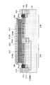
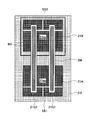
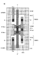
- FIG. 13B is a plan view of a single n-channel Dt-MOS transistor 40 used in the semiconductor logic integrated circuit 20 of this embodiment, and FIG. 13C is along the line XX ′ of the MOS transistor of FIG. 13B. A cross-sectional view is shown.
- a deep n-type well 41DNW is formed under the element region 41NMOS defined by the element isolation structure 41I corresponding to the element isolation structure 21I.
- a polysilicon is formed corresponding to the deep n-type well 21DNW.
- polysilicon corresponding to the polysilicon pattern 21G1 or 21G2 and serving as the gate electrode of the n-channel MOS transistor 40 is formed.
- a p-type well 41PW is formed directly below the pattern 41G along the polysilicon silicon pattern 41G corresponding to the p-type well 21PW.
- a p-type channel doped region NVT is formed on the surface of the p-type well 41PW.
- the gate electrode 41G is formed on the element region 41NMOS via a gate insulating film 41Gox.
- an n + type source diffusion region and an n + type drain diffusion region are formed on one side and the other side of the gate electrode 41G, respectively, using Mask1 shown in FIG. 13B as an ion implantation mask.
- a source contact S and a drain contact D are formed respectively.
- the gate electrode 41G is doped n + type on the element region 41NMOS.
- the n-channel MOS transistor according to the present embodiment is similar to the n-channel MOS transistor NMOS1 or NMOS2 whose cross section was previously shown in FIG. It has the same insulating pattern as 21I1 to 21I3, and the source diffusion region and the drain diffusion region are formed epitaxially by regrowth on the insulating pattern.
- the element region 41NMOS defined by the element isolation structure 41I has an extension 41ex on a part thereof, and the head 41Gh of the gate electrode 41G is formed on the extension 41ex.
- the extension portion 41ex is partially covered via the gate insulating film 41Gox.
- the head portion 41Gh and the extension portion 41ex of the gate electrode 41G are doped p + type using Mask2 shown in FIG. 13B as an ion implantation mask.
- an insulating pattern 41i similar to the insulating patterns 21I7 to 21I10 in the previous embodiment is formed continuously with the element isolation structure 21I, and the insulating pattern 41i is formed on the insulating pattern 41i.
- an epitaxial layer of silicon is formed by regrowth to form the extension 41ex.
- a silicide layer 45 is formed on the surface of the source diffusion region / drain diffusion region in the polysilicon pattern 41G and the element region 41NMOS, and further on the surface of the extension 41ex, and the gate electrode 41G is formed by a via plug VC. , And electrically connected to the extending portion 41ex.
- the silicide layer 45s formed on the extending portion 41ex is separated from the silicide layer 45 formed on the surface of the element region 41NMOS by the head portion 41Gh of the polysilicon pattern 41G. Therefore, a short circuit between the via contact VC and the source diffusion region or the drain diffusion region can be avoided without forming the silicide block patterns SB1 and SB2 as in the previous embodiment.
- a p-channel Dt-MOS transistor can be formed.
- the deep n-type well 41DNW is not used.
- the configuration of the p-channel Dt-MOS transistor is clear from the description of the previous embodiments such as FIGS. 13B and 13C and FIGS. 10A to 10V, and further description is omitted.
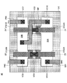
- FIG. 13D is a plan view showing a layout of the inverter 60 using the n-channel Dt-MOS transistor 41 and the corresponding p-channel Dt-MOS transistor of FIGS. 13B and 13C
- FIG. 13E is a line Y in FIG. 13D. A cross-sectional view along -Y ′ is shown.
- the inverter 60 includes an n-channel Dt-MOS transistor NMOS having the same configuration as the n-channel Dt-MOS transistor NMOS1 or NMOS2 in FIG. 5 and a p-channel Dt-MOS transistor in FIG.
- the p-channel Dt-MOS transistor PMOS has the same configuration as the PMOS1 or PMOS2, and the n-channel Dt-MOS transistor NMOS is formed in an element region 61A defined by an element isolation region 21I in the silicon substrate 21.
- the p-channel Dt-MOS transistor PMOS is formed in the element region 61B defined by the element isolation region 21I in the silicon substrate 21.
- the element region 61A has an extension part 61Aex in a part thereof, and the element region 61B has an extension part 61Bex in a part thereof, and the extension parts 61Aex and 61Bex are connected to each other.
- the region 61A and the element region 61B constitute a single active region.
- a deep n-type well 61DNW is formed below the extended portion 61Aex corresponding to the deep n-type well 21DNW.
- a polysilicon gate electrode 61G1 extends over the element region 61A through the gate insulating film 61Gox1 including the extending portion 61Aex, and the p-type well 21PW is directly under the polysilicon gate electrode 61G1. Corresponding to p-type well 61PW extends.
- a polysilicon gate electrode 61G2 extends through the gate insulating film 61Gox2 including the extending portion 61Bex, and the n-type is directly below the polysilicon gate electrode 61G2.
- An n-type well 61NW extends corresponding to the well 21NW.
- the channel doped region NVT of the n-channel MOS transistor NMOS is formed on the surface of the p-type well 61PW, and the p-channel MOS transistor is formed on the surface of the n-type well 61NW.
- a PMOS channel doped region PVT is formed.
- an insulating pattern 61i similar to the insulating patterns 21I7 to 21I10 in the previous example is continuously formed under the extending portions 61Aex and 61Bex, and the insulating pattern
- An epitaxial layer of silicon is formed on the silicon 61i by regrowth to form the extending portions 61Aex and 61Bex.
- the silicon epitaxial layer is doped p + type in the extension 61Aex to form an ohmic contact region 61P +, and is doped n + in the extension 61Bex to form an ohmic contact region 61N +.
- Silicide layers 65 are formed on the surfaces of the polysilicon gate electrodes 61G1 and 61G2, and silicide layers 65 are continuously formed on the surfaces of the ohmic contact regions 61P + and 61N + from the ohmic contact regions 61P + to 61N +. Via plugs 61in are formed on the ohmic contact regions 61P + and 61N + so as to bridge the gate electrodes 61G1 and 61G2.
- an input voltage signal is supplied to the via plug 61in, and the wiring pattern 61WR is connected to the drain region D of the p-channel Dt-MOS transistor PMOS and the drain region D of the n-channel Dt-MOS transistor NMOS.
- the element of FIG. 13D operates as an inverter.
- the silicide layer 65 formed on the ohmic contact regions 61P + and 61N + includes the source region S or drain region D of the element region 61A, and further the source region S or drain region D of the element region 61B. Since the silicide layer formed on the gate electrode is separated by the gate insulating film 61Gox1 directly below the polysilicon gate electrode 61G1 and the gate insulating film 61Gox2 directly below the polysilicon gate electrode 61Gox2, the silicide block pattern as in the previous embodiment is used. There is no need to form SB1 and SB2.
- FIG. 13F shows a configuration of a two-input NAND device 80 according to a modification of the two-input NAND device 40 of FIG. 4 using the inverter structure of FIGS. 13D and 13E.
- the parts described above are denoted by corresponding reference numerals, and the description thereof is omitted.
- two polysilicon patterns 21G1A and 21G1B are used instead of the polysilicon pattern 21G1 of FIG. 4, and two polysilicon patterns are used instead of the polysilicon pattern 21G2.
- 21G2A and 21G2B are used.
- the cross section taken along lines Z1-Z1 ′ and Z2-Z2 ′ in FIG. 13F has the same structure as the cross section of FIG. 13E, and the via contact VC5 is the first signal.
- the polysilicon patterns 21G1A and 21G1B are connected to the p-type ohmic region 21P + 1 and the n-type ohmic region 21N + 1, respectively.
- the via contact VC6 constitutes the second signal input terminal, and at the same time, the polysilicon patterns 21G2A and 21G2B are connected to the p-type ohmic region 21P + 2 and the n-type ohmic region 21N + 2, respectively.
- the via contacts VC1 to VC4 in FIG. 4 are omitted.
- the insulating regions 21I1 to 21I10 are formed by forming a trench in the silicon bulk substrate 21, and depositing a silicon oxide film on the formed trench. It is not limited to such a specific manufacturing method, and can be formed by ion implantation of oxygen ions as described below.
- FIG. 14A corresponds to the steps of FIGS. 10C and 10D.
- oxygen ions are implanted into the surfaces of the polysilicon patterns 21G1 and 21G2 instead of the hard mask pattern 21OM.
- the cover film 21M for preventing the film is formed with a film thickness of 30 to 50 nm using, for example, a tungsten (W) film.
- oxygen ions O + are ion-implanted into the structure of FIG. 14A, using the cover film 21M as a mask, for example, at an acceleration voltage of 10 to 60 keV and a dose of 1 ⁇ 10 16 cm ⁇ 2 or more.
- Oxygen doped regions 21J1 to 21J6 are formed corresponding to the insulating regions 21I1 to 21I6.
- similar oxygen doped regions are also formed corresponding to the other insulating regions 21I7 to 21I10.
- the depth of the oxygen doped regions 21J1 to 21J6 can be controlled by an acceleration voltage.
- the depth of the upper ends of the oxygen doped regions 21J1 to 21J6 can be controlled to 27 nm. Further, when an acceleration voltage of 60 keV is used, the depth of the upper ends of the oxygen doped regions 21J1 to 21J6 can be controlled to 140 nm.
- RTA rapid thermal processing
- MSA millisecond thermal processing
- Oxygen atoms introduced in the regions 21J1 to 21J6 react with Si atoms to convert the oxygen doped regions 21J1 to 21J6 into insulating regions 21I1 to 21I6 made of silicon oxide films, respectively.
- the insulating regions 21I7 to 21I10 are formed in the same manner.
- FIG. 14C By performing the processes of FIG. 10O and FIG. 10P and thereafter, the semiconductor logic circuit device 20 of FIG. Can be manufactured.
- FIGS. 15A to 15D show a third embodiment. However, FIGS. 15A to 15D are subsequent to the steps of FIGS. 10G and 10H and replace the steps of FIGS. 10I to 10N.
- a layer 21Ge in which a SiGe mixed crystal layer, a Ge layer, and a SiGe mixed crystal layer are sequentially stacked is formed below the trenches T1 to T8.
- the upper end of the layer 21G2 is formed with a thickness exceeding the upper end of the p-type well 21PW or the n-type well 21NW by sputtering or CVD.
- the layer 21Ge thus formed has a SiGe mixed crystal layer interposed between the underlying silicon substrate and the Ge layer, and a SiGe mixed crystal layer formed on the Ge layer.
- an epitaxial layer of silicon can be easily formed.
- the n-channel MOS transistor NMOS1 is a part of the AA ′ section in FIG. 4, and the p-channel MOS transistor PMOS1 is a part of the BB ′ section in FIG.
- a single crystal silicon epitaxial layer 21ep is formed on the layer 21Ge by performing epitaxial growth.
- the single crystal silicon epitaxial layer 21ep can be formed under the conditions described above with reference to FIGS. 10M and 10N.
- an opening 21eo exposing the Ge layer in the underlying layer 21Ge is formed in the single crystal silicon epitaxial layer 21ep.
- the silicon bulk substrate 21 is heat-treated at a temperature of 600 ° C. in an oxygen atmosphere.
- the Ge layer constituting the layer 21Ge is vaporized as GeO and is discharged out of the system from the opening 21eo.
- a space 21V is formed under the single crystal silicon epitaxial layer 21ep instead of the insulating regions 21I1 to 21I10 in the previous embodiment.
- the space 21V thus formed exhibits the same insulating action as that of the insulating regions 21I1 to 21I10.
- the relative permittivity is 1.0
- the n-channel MOS transistors NMOS1 and NMOS2 and the p-channel MOS transistor PMOS1 and The parasitic capacitance of the PMOS 2 is reduced, and a favorable effect of improving the respective operation speeds can be obtained.
- FIG. 16 is a plan view showing a configuration of a logic integrated circuit device 60 according to the fourth embodiment. However, in FIG. 16, the parts described above are denoted by the same reference numerals, and description thereof is omitted.
- the semiconductor logic circuit device 60 is a NOR circuit device.
- the element regions 21A and 21B are replaced, and the n-channel MOS transistor NMOS1 and the p-channel MOS transistor are replaced.
- the PMOS 2 is replaced, and the n-channel MOS transistor NMOS 2 and the p-channel MOS transistor PMOS 1 are replaced.
- the n-channel MOS transistor NMOS1 and the n-channel MOS transistor NMOS2, and the p-channel MOS transistor PMOS1 and the p-channel MOS transistor PMOS2 are all Dt-MOS transistors and are formed on the silicon bulk substrate. .
- the Dt-MOS configuration n-channel MOS transistors NMOS1 and NMOS2 in FIG. 4 are connected in series, or the Dt-MOS configuration p-channel MOS transistors PMOS1 and PMOS2 in FIG. 16 are connected in series. It can be used alone, for example, as a semiconductor device such as a transfer gate.
- FIG. 17 shows an equivalent circuit diagram of such a transfer gate composed of Dt-MOS transistors NMOS1 and NMOS2.
Landscapes
- Metal-Oxide And Bipolar Metal-Oxide Semiconductor Integrated Circuits (AREA)
- Insulated Gate Type Field-Effect Transistor (AREA)
- Semiconductor Integrated Circuits (AREA)
Abstract
半導体装置は、シリコンバルク基板上の素子領域中に形成された第1および第2のDt-MOSトランジスタを含み、前記第1および第2のDt-MOSトランジスタは、一つの拡散領域を共有して形成され、それぞれの拡散領域の下には対応する絶縁領域が形成される。前記第1および第2のDt-MOSトランジスタのゲート電極の下には第1および第2のボディ領域がそれぞれ延在し、前記絶縁領域の下端は前記第1および第2のボディ領域の下端よりも深く形成され、前記第1および第2のボディ領域の下端は前記拡散領域の下端よりも深く形成される。
Description
本発明は一般に半導体装置に係り、特にダイナミックスレッショルドMOSトランジスタ(以下Dt-MOSトランジスタと表記する)を使った半導体装置、およびDt-MOSトランジスタを使った半導体論理回路装置に関する。
Dt-MOSトランジスタは、ゲート電極を、チャネル領域が形成される半導体層ないしウェル領域に短絡させ、入力信号を前記ゲート電極とチャネル領域が形成される半導体層ないしウェル領域とに同時に印加することにより、低い閾値ながら、低いオフ電流と大きなオン電流を実現でき、低い電源電圧での低消費電力動作に適したMOSトランジスタである。チャネル領域が形成される半導体層ないしウェル領域を、ボディとよぶこともある。
図1は、一般的なDt-MOSトランジスタの原理を説明する図、図2は、前記図1のDt-MOSトランジスタ10の動作特性を示すグラフである。
図1を参照するに、この例ではDt-MOSトランジスタ10はnチャネルMOSトランジスタであり、n型にドープされたソース領域11Sおよびドレイン領域11Dを含むp型ウェル11Pが形成されたシリコン基板11上に形成されており、前記シリコン基板11上には、前記ソース領域11Sとドレイン領域11Dとの間のチャネル領域11C上に、ゲート絶縁膜12を介して例えばn型ポリシリコンよりなるゲート電極13が形成されている。
図1のDt-MOSトランジスタ10では、さらに前記ゲート電極13が前記p型ウェル11P、すなわちボディと電気的に接続されており、ゲート電極13に印加される信号電圧が、前記ボディ11Pにも印加される。その結果、前記信号電圧は前記Dt-MOSトランジスタ10の閾値電圧を低下させるように作用し、Dt-MOSトランジスタ10の動作特性は、前記信号電圧の増大と共に、閾値電圧が低いMOSトランジスタの動作特性に漸近する。このため、前記Dt-MOSトランジスタ10は低い信号電圧でスイッチオンする。
一方、信号電圧が0Vあるいはその近傍の低電圧である場合には、前記ボディ11Pの電位が0Vあるいはその近傍となり、Dt-MOSトランジスタ10の動作特性は、高い閾値電圧を有するMOSトランジスタの動作特性に漸近する。すなわち前記Dt-MOSトランジスタ10の閾値電圧は、通常の、高い閾値電圧を有するnチャネルMOSトランジスタのものと変わらず、その結果、Dt-MOSトランジスタ10は図2に示すように低いオフ電流ないしリーク電流で特徴づけられるスイッチオフ動作を示す。
このようなDt-MOSトランジスタでは、図1中に囲んで示したソース領域11Sとボディ11Pの間の接合部11Jが順方向バイアスされるため、前記ソース領域11S、ドレイン領域11Dの間に大きな電源電圧を印加することができず、前記基板11としてシリコン基板を使った場合、前記電源電圧は、シリコンpn接合のビルトインポテンシャルに対応した0.7V以下に設定する必要があるという制約が課せられる。
なお上記の説明は、上記のp型およびn型を反転させたpチャネルMOSトランジスタの場合にも、同様に成立する。
Assaderaaghi, F. et al., IEEE Electron Device Lett.15, pp.510- (1994)
シャープ技報第79号・2001年4月
このようなDt-MOSトランジスタを通常の、単結晶シリコンインゴットから切り出されたシリコン基板(以下、シリコンバルク基板と称する)上に形成した場合には、ソースやドレインのリーク電流が増大してしまう問題があり、またソース領域あるいはドレイン領域と前記ボディとの間で接合容量が増大し、時定数の影響でDt-MOSトランジスタの動作速度が低下する問題が生じる。このため従来、Dt-MOSトランジスタは一般にSOI基板上に形成されていた(非特許文献1)。先の図2の特性は、非特許文献2に記載された、このようなSOI基板上に形成されたDt-MOSSトランジスタについてのものである。
しかし、単体のDt-MOSならばともかく、単一の基板上に一つのシステムを搭載するSoC(システムオンチップ)のような半導体装置では、同じ基板上に、Dt-MOSトランジスタのようにダイナミックスレッショルド動作をするトランジスタ以外にも、他の様々なトランジスタを集積する必要があり、そのなかにはダイナミックスレッショルド動作をさせたくない入出力トランジスタやアナログ用途のトランジスタなどが含まれることがある。
このような場合、これらのトランジスタについては、個別にコンタクトを設けてボディを接地するなどしてボディ電位を固定する対策が必要となるが、このような構成では、高価なSOI基板の使用に伴う費用の増大の他に、集積密度が低下したり、製造プロセスが複雑になったりする問題が生じてしまう。また入力信号が高周波信号となると、ボディの電位が入力信号の変化に追従できなくなるという問題も生じる。
またDt-MOSトランジスタをSOI基板上に形成した場合には、ボディを構成するシリコン膜11Pの膜厚が薄くなり、このためボディの抵抗が増大してしまい、時定数の効果でトランジスタの動作速度が低減する問題が生じる。
従来、シリコンバルク基板上にDt-MOSトランジスタを形成しようとする試みも行われている。例えば非特許文献2には、ソース領域およびドレイン領域を素子分離構造上に、エレベーテッド・ソース/ドレイン構造として形成し、素子面積の増大を回避しつつ、ソース領域あるいはドレイン領域とボディとの間の接合容量を低減する構成が提案されている。
しかし、この従来の構造では、ソースリーク電流の増大や接合容量の増大の問題は解決するものの、ボディとソース領域あるいはドレイン領域との間の電流経路が絞られるため、ソース抵抗が増大してしまい、またゲート電極がソース領域あるいはドレイン領域と絶縁膜を介して対向して形成されるため、ゲート電極とソース領域あるいはドレイン領域との間の寄生容量が増大してしまう問題点があり、またさらに、製造工程が複雑になる問題点がある。
一実施形態によれば半導体装置は、素子分離領域により素子領域を画成されたシリコンバルク基板と、前記素子領域中に形成された第1のダイナミックスレッショルドMOSトランジスタと、前記素子領域中に形成された第2のダイナミックスレッショルドMOSトランジスタと、を含み、前記素子領域は第1の導電型を有するウェルよりなり、前記第1のダイナミックスレッショルドMOSトランジスタは、前記シリコンバルク基板の表面上に第1のゲート絶縁膜を介して形成された第1のゲート電極と、前記ウェル中、前記第1のゲート電極の第1の側に形成された第1の拡散領域と、前記第1のゲート電極に対し前記第1の拡散領域と反対の第2の側に形成された第2の拡散領域とを有し、前記第2のダイナミックスレッショルドMOSトランジスタは、前記シリコンバルク基板の表面上、前記第1のゲート電極の前記第2の側に、第2のゲート絶縁膜を介して形成された第2のゲート電極と、前記ウェル中、前記第2のゲート電極に対し前記第1のゲート電極の側に形成された第3の拡散領域と、前記第2のゲート電極に対し前記第3の拡散領域と反対側に形成された第4の拡散領域とを有し、前記第1および第2のゲート電極および前記第1~第4の拡散領域は、前記ウェルとは逆の第2の導電型を有し、前記第2の拡散領域と前記第3の拡散領域とは、前記ウェル中に形成された同一の拡散領域より構成されており、前記第1~第4の拡散領域の下には、それぞれの下端部に接して第1~第4の絶縁領域がそれぞれ形成されており、前記第2の絶縁領域と前記第3の絶縁領域とは、同一の絶縁領域より構成されており、前記第1の絶縁領域と前記第2の絶縁領域の間には、前記第1のゲート電極に沿って、前記第1のダイナミックスレッショルドMOSトランジスタのボディを構成する前記第1の導電型の第1のボディ領域が、前記素子領域の一部として延在しており、前記第3の絶縁領域と前記第4の絶縁領域の間には、前記第2のゲート電極に沿って、前記第2のダイナミックスレッショルドMOSトランジスタのボディを構成する前記第1の導電型の第2のボディ領域が、前記素子領域の一部として延在しており、前記第1のゲート電極は前記第1の領域に接続されており、前記第2のゲート電極は前記第2の領域に接続されており、前記第1~第4の絶縁領域の下端は、前記第1および第2のボディ領域の下端よりも深い位置に設定されており、前記第1および第2のボディ領域の下端は、前記第1~第4の拡散領域の下端よりも深い位置に設定されている。
上記実施形態によれば、二つのDt-MOSトランジスタを含む半導体装置において、それぞれのDt-MOSトランジスタのソースあるいはドレインとなる拡散領域の直下に絶縁領域が、それぞれの絶縁領域が対応する拡散領域の下端に接するように形成されており、その結果、これら拡散領域に伴う接合容量が低減され、また接合リーク電流が減少する。さらに同一の素子領域中で隣接する二つのDt-MOSトランジスタにおいて、一方のDt-MOSトランジスタの拡散領域を他方のDt-MOSトランジスタの拡散領域と兼用することにより、素子面積を低減することができる。さらに前記絶縁領域の下端を、それぞれのDt-MOSトランジスタのボディ領域の下端よりも深く形成することにより、これら二つのDt-MOSトランジスタのボディ領域を電気的に独立させることが可能となる。またこれらボディ領域の下端をそれぞれの拡散領域の下端よりも深く形成することにより、拡散領域と素子領域を構成するウェルとの間の短絡を抑制することが可能となる。
[第1の実施形態]
以下、Dt-MOSトランジスタを使った第1の実施形態による半導体論理回路装置20について説明する。
以下、Dt-MOSトランジスタを使った第1の実施形態による半導体論理回路装置20について説明する。
図3は、第1の実施形態による半導体論理回路装置20のその等価回路図を示し、図4はそのレイアウトを示す平面図である。また図5~図9は、前記図4中、それぞれ線A-A',B-B',C-C',D-D',E-E'に沿った断面図を示す。
図3の等価回路図からわかるように、前記半導体論理回路装置20は二入力NAND装置であり、並列接続された二つのpチャネルMOSトランジスタPMOS1およびPMOS2と、これに対し直列に接続された二つのnチャネルMOSトランジスタNOS1およびNMOS2より構成され、本実施形態では、これらのpチャネルMOSトランジスタPMOS1およびPMOS2,nチャネルMOSトランジスタNMOS1およびNMOS2は、p-型にドープされたシリコンバルク基板21(図5~図9を参照)上に形成されている。
前記並列接続されたpチャネルMOSトランジスタPMOS1およびPMOS2のソースSは共通に電源VCCに接続され、また前記pチャネルMOSトランジスタPMOS1およびPMOS2のドレインDは共通に、前記nチャネルMOSトランジスタNMOS1のドレインDに接続される。また前記nチャネルMOSトランジスタNMOS1のソースSは前記nチャネルMOSトランジスタNMOS2のドレインDに接続され、前記nチャネルMOSトランジスタNMOS2のソースSは接地電源GNDに接続されている。
また前記pチャネルMOSトランジスタPMOS2および前記nチャネルMOSトランジスタNMOS1のそれぞれのゲート電極には第1の入力信号IN1が供給され、前記pチャネルMOSトランジスタPMOS1および前記nチャネルMOSトランジスタNMOS2のそれぞれのゲート電極には第2の入力信号IN1が供給され、論理出力信号が、前記pチャネルMOSトランジスタPMOS1およびPMOS2のドレインDとnチャネルMOSトランジスタNMOS1のドレインDの接続ノードNにおいて得られる。
次に図4の平面図を参照するに、前記シリコンバルク基板21中にはSTI構造の素子分離領域21Iにより第1の素子領域21Aおよび第2の素子領域21Bが画成されており、前記素子領域21Aには、ポリシリコンパタ―ン21G1をゲート電極として前記nチャネルMOSトランジスタNMOS1が形成されており、またポリシリコンパタ―ン21G2をゲート電極として前記nチャネルMOSトランジスタNMOS2が形成されている。
前記ポリシリコンパタ―ン21G1および21G2はさらに前記素子領域21Bへと延在し、前記素子領域21Bでは前記ポリシリコンパタ―ン21G1およびポリシリコンパタ―ン21G2をそれぞれのゲート電極として、前記pチャネルMOSトランジスタPMOS2およびPMOS1が形成されている。
前記ポリシリコンパタ―ン21G1はビアコンタクトVC1およびVC2において、それぞれ前記素子領域21Aおよび21Bに電気的に接続されており、またポリシリコンパタ―ン21G2はビアコンタクトVC3およびVC4において、それぞれ前記素子領域21Aおよび21Bに電気的に接続されている。これにより、前記nチャネルMOSトランジスタNMOS1およびNMOS2、およびpチャネルMOSトランジスタPMOS1,PMOS2はいずれも、先に図2で説明したようなダイナミックスレッショルド動作を示す。
さらに前記pチャネルMOSトランジスタPMOS1はそのドレインを、前記pチャネルMOSトランジスタPMOS2のドレインと共有し、前記nチャネルMOSトランジスタNMOS1はそのソースをnチャネルMOSトランジスタNMOS2のドレインと共有している。これにより、前記pチャネルMOSトランジスタPMOS1,PMOS2およびnチャネルMOSトランジスタNMOS1,NMOS2を、それぞれの素子領域中に、素子分離構造で分離して形成した場合に比べて、前記半導体論理回路装置20の素子面積を大きく低減することが可能となる。
また前記ポリシリコンパタ―ン21G1には、前記素子領域21Aと21Bの間の素子分離領域21I上において、図4の平面図では見えないが、前記入力信号Aを供給されるビアコンタクトVC5が形成されている(図7参照)。同様に前記ポリシリコンパタ―ン21G2には、前記素子領域21Aと21Bの間の素子分離領域21I上において、前記入力信号Bを供給されるビアコンタクトVC6が形成されている。
さらに前記図3の回路を構成するため、前記素子領域21Bには、前記pチャネルMOSトランジスタPMOS1およびPMOS2のそれぞれのソース領域Sに、それぞれの電源パタ―ンPW1およびPW2から電源電圧VCCを供給するビアコンタクトVC7およびVC8が形成されており、さらに共通接続された前記pチャネルMOSトランジスタPMOS1およびPMOS2のドレインDは、前記nチャネルMOSトランジスタNMOS1のドレインDに設けられたビアコンタクトVC10に、ビアコンタクトVC9および配線パタ―ンWPを介して接続されている。また前記nチャネルMOSトランジスタNMOS2のソース領域が、ビアコンタクトVC11および接地パタ―ンGD1を介して、GNDに接続されており、前記半導体論理回路20の出力は、前記配線パタ―ンWP上に得られる。
なお図4の平面図において、前記素子領域21Aには、ビアコンタクトVC1およびVC3を相互に分離し、またビアコンタクトVC10およびVC11からも分離する絶縁パターンSB1が形成されている。前記絶縁パターンSB1はシリサイドブロック構造として作用し、その結果、前記素子領域21Aにシリサイド層(図示せず)が形成された場合でも、ビアコンタクトVC1とビアコンタクトVC3,VC10,VC11との短絡が回避される。同様に前記絶縁パターンSB1を形成した結果、前記素子領域21Aにシリサイド層(図示せず)が形成された場合でも、ビアコンタクトVC3とビアコンタクトVC1,VC10,VC11との短絡が回避される。
同様に図4の平面図において、前記素子領域21Bには、ビアコンタクトVC2およびVC4を相互に分離し、またビアコンタクトVC7およびVC8からも分離する絶縁パターンSB2が形成されている。前記絶縁パターンSB2もシリサイドブロック構造として作用し、その結果、前記素子領域21Bにシリサイド層(図示せず)が形成された場合でも、ビアコンタクトVC2とビアコンタクトVC4,VC7,VC8との短絡が回避される。同様に前記絶縁パターンSB2を形成した結果、前記素子領域21Bにシリサイド層(図示せず)が形成された場合でも、ビアコンタクトVC4とビアコンタクトVC2,VC7,VC8との短絡が回避される。
前記絶縁パターンSB1,SB2は、前記ポリシリコンパタ―ン21G1,21G2に側壁絶縁膜を形成する際に、マスクプロセスを追加することで形成することができる。
図5は、前記図4の平面図中の線A-A'に沿った断面図を示す。
図5を参照するに、前記素子領域21Aには深いn型ウェル21DNWが形成されており、前記n型ウェル21DNWの表面部分には、前記ポリシリコンパタ―ン21G1により構成されるn型ドープゲート電極23G1Nの直下、および前記ポリシリコンパタ―ン21G2により構成されるn型ドープゲート電極23G2Nの直下にそれぞれ対応して、前記nチャネルMOSトランジスタNMOS1およびNMOS2のそれぞれのボディ21BY1および21BY2を構成する浅いp型ウェル21PWが形成されている。
また前記p型ボディ21BY1および21BY2のそれぞれの表面部分には、前記ゲート電極23G1N直下の前記MOSトランジスタNMOS1のチャネル領域CH1および前記ゲート電極23G2N直下の前記MOSトランジスタNMOS2のチャネル領域CH2に対応して、閾値制御のためのp型チャネルドープ領域21NVT1および21NVT2がそれぞれp型注入領域21NVTの一部分として形成されている。なお前記p型チャネルドープ領域21NVT1,21NVT2は、前記ボディ21BY1および21BY2を構成するp型ウェル21PWにより兼用することも可能である。
図4に示すように、前記ゲート電極23G1Nを構成するポリシリコンパタ―ン21G1は、前記ビアコンタクトVC1において前記ボディ21BY1に電気的に接続され、その結果、前記ボディ21BY1にも、前記ゲート電極23G1Nに印加される入力信号IN1が同時に印加され、前記nチャネルMOSトランジスタNMOS1はダイナミックスレッショルド動作を行う。同様に前記ゲート電極23G2Nを構成するポリシリコンパタ―ン21G2は、前記ビアコンタクトVC3において前記ボディ21BY2に電気的に接続され、その結果、前記ボディ21BY2にも、前記ゲート電極23G2Nに印加される入力信号IN2が同時に印加され、前記nチャネルMOSトランジスタNMOS2は、例えば先に図2で説明したようなダイナミックスレッショルド動作を行う。
前記ゲート電極21G1Nおよび21G2Nは、前記シリコンバルク基板21上に、それぞれゲート絶縁膜22Ox1および22Ox2を介して形成されており、前記深いウェル21DNW中には、前記チャネル領域CH1の第1の側に前記nチャネルMOSトランジスタNMOS1のドレインとなるn型拡散領域21DN1が、また前記チャネル領域CH1を挟んで前記n型拡散領域21DN1と対向する側には、前記nチャネルMOSトランジスタNMOS1のソースとなるn型拡散領域21SN1が形成されている。
同様に前記深いウェル21DNW中には、前記チャネル領域CH2の第1の側に前記nチャネルMOSトランジスタNMOS2のドレインとなるn型拡散領域21DN2が、また前記チャネル領域CH2を挟んで前記n型拡散領域21DN2と対向する側には、前記nチャネルMOSトランジスタNMOS2のソースとなるn型拡散領域21SN2が、それぞれ形成されている。ここで前記n型拡散領域21SN1とn型拡散領域21DN2とは、実際には同一のn型拡散領域より構成されており、これにより、本実施形態では、先に説明したように前記半導体論理回路20の占有面積を縮小することが可能である。
さて、図5の構造では、前記n型拡散領域21DN1、前記n型拡散領域21SN1すなわちn型拡散領域21DN2、および前記n型拡散領域21SN2の直下に、シリコン酸化膜よりなる絶縁領域21I1,21I2および21I3がそれぞれ形成されていることに注意すべきである。
前記絶縁領域21I1は、隣接する素子分離領域21Iに連続し、また前記絶縁領域21I3は、隣接する素子分離領域21Iに連続しており、また前記絶縁領域21I1,21I2および21I3は、それぞれの下端が前記ボディ21BY1および21BY2を構成する浅いp型ウェル21PWの下端よりも深くなるように形成されている。その結果、前記ボディ21BY1および21BY2は相互に電気的に分離され、前記入力信号IN1およびIN2が干渉する問題は生じない。
また前記n型拡散領域21DN1、21SN1、従って21DN2、および21SN2の下端は、前記浅いp型ウェル21PWの下端よりも浅く形成されており、これらのn型拡散領域が、その下のn型ウェル21NWと短絡する恐れはない。
さらに前記図5の構成では、前記シリコンバルク基板21上に層間絶縁膜23,24が積層され、前記拡散領域21DN1に前記ビアコンタクトVC10が、前記層間絶縁膜23,24を貫通してコンタクトしている。同様に、前記拡散領域21SN2には前記ビアコンタクトVC11が、前記層間絶縁膜23,24を貫通してコンタクトしている。前記ビアコンタクトVC10には、前記層間絶縁膜24上に形成された配線パタ―ンWPがコンタクトし、またビアコンタクトVC11には、前記層間絶縁膜24上に前記接地電源GNDに接続されて形成された配線パタ―ンGD1が接続されている。
図6は、前記図4の平面図中の線B-B'に沿った断面図を示す。
図6を参照するに、前記素子領域21Bの表面部分には、前記ポリシリコンパタ―ン21G1により構成されるp型ドープゲート電極23G2Pの直下、および前記ポリシリコンパタ―ン21G2により構成されるp型ドープゲート電極21G1Pの直下にそれぞれ対応して、前記pチャネルMOSトランジスタPMOS2およびPMOS1のそれぞれのボディ21BY4および21BY3を構成する浅いn型ウェル21NWが形成されている。
また前記n型ボディ21BY3および21BY4のそれぞれの表面部分には、前記ゲート電極23G1P直下の前記MOSトランジスタPMOS1のチャネル領域CH3および前記ゲート電極23G1P直下の前記MOSトランジスタPMOS2のチャネル領域CH4に対応して、閾値制御のためのn型チャネルドープ領域21PVT1および21PVT2がそれぞれn型注入領域PVTの一部分として形成されている。なお前記n型チャネルドープ領域21PVT1,21PVT2は、前記ボディ21BY3および21BY4を構成するn型ウェル21NWにより兼用することも可能である。
図4に示すように、前記ゲート電極23G2Pを構成するポリシリコンパタ―ン21G1は、前記ビアコンタクトVC2において前記ボディ21BY4に電気的に接続され、その結果、前記ボディ21BY4にも、前記ゲート電極23G2Pに印加される入力信号IN1が同時に印加され、前記pチャネルMOSトランジスタPMOS2はダイナミックスレッショルド動作をする。同様に前記ゲート電極23G1Pを構成するポリシリコンパタ―ン21G2は、前記ビアコンタクトVC4において前記ボディ21BY3に電気的に接続され、その結果、前記ボディ21BY3にも、前記ゲート電極23G1Pに印加される入力信号IN2が同時に印加され、前記pチャネルMOSトランジスタPMOS1は、例えば先に図2で説明したようなダイナミックスレッショルド動作を行う。
前記ゲート電極21G2Pおよび21G1Pは、前記シリコンバルク基板21上に、それぞれゲート絶縁膜22Ox3および22Ox4を介して形成されており、前記p型シリコンバルク基板21中には、前記チャネル領域CH4の第1の側に前記pチャネルMOSトランジスタPMOS2のドレインとなるp型拡散領域21SP2が、また前記チャネル領域CH4を挟んで前記p型拡散領域21SP2と対向する側には、前記pチャネルMOSトランジスタPMOS2のソースとなるp型拡散領域21DP2が形成されている。
同様に前記p型シリコンバルク基板21中には、前記チャネル領域CH3の第1の側に前記pチャネルMOSトランジスタPMOS1のドレインとなるp型拡散領域21DP1が、また前記チャネル領域CH3を挟んで前記p型拡散領域21DP1と対向する側には、前記pチャネルMOSトランジスタNMOS1のソースとなるn型拡散領域21SP1が、それぞれ形成されている。ここで前記p型拡散領域21DP2とp型拡散領域21DP1とは、実際には同一のp型拡散領域より構成されており、これらには、図4におけるビアコンタクトVP9が電気的に接続されて形成されている。このように前記p型拡散領域21DP2とp型拡散領域21DP1とを、同一のp型拡散領域より構成することにより、本実施形態では、先に説明したように前記半導体論理回路20の占有面積を縮小することが可能である。
前記ビアコンタクトVP9は前記層間絶縁膜23,24を貫通して延在し、前記層間絶縁膜24上に形成された配線パタ―ンWPに接続される。
図6の構造では、前記p型拡散領域21SP1、前記p型拡散領域21DP1すなわちp型拡散領域21DP2、および前記p型拡散領域21SP2の直下に、シリコン酸化膜よりなる絶縁領域21I4,21I5および21I6がそれぞれ形成されていることに注意すべきである。
前記絶縁領域21I4は、隣接する素子分離領域21Iに連続し、また前記絶縁領域21I6も隣接する素子分離領域21Iに連続しており、また前記絶縁領域21I3,21I4および21I5は、それぞれの下端が前記ボディ21BY3および21BY4を構成する浅いn型ウェル21NWの下端よりも深くなるように形成されている。その結果、前記ボディ21BY3および21BY4は相互に電気的に分離され、前記入力信号IN1およびIN2が干渉する問題は生じない。
また前記p型拡散領域21SP1、21DP1、従って21DP2、および21SP2の下端は、前記浅いウェル21NWの下端よりも浅く形成されており、これらのp型拡散領域が、その下のp型シリコンバルク基板21と短絡する恐れはない。
さらに前記図6の構成では、前記拡散領域21SP2に前記ビアコンタクトVC1が、前記層間絶縁膜23,24を貫通してコンタクトしている。同様に、前記拡散領域21SP1には前記ビアコンタクトVC8が、前記層間絶縁膜23,24を貫通してコンタクトしている。前記ビアコンタクトVC7には、前記層間絶縁膜24上に形成された電源配線パタ―ンPW1がコンタクトし、またビアコンタクトVC8には、前記層間絶縁膜24上に前記電源配線パタ―ンPW2が接続されている。
図7は、前記図4中、線C-C'に沿った前記半導体論理回路装置20の断面図を示す。
図7を参照するに、前記素子領域21Aにおいては前記ポリシリコンパタ―ン21G1の一部により構成されるゲート電極23G1Nの直下に、前記チャネルドープ領域NVT1を含む浅いp型ウェル21PWが形成されており、前記浅いp型ウェル21PWには、前記ポリシリコンパタ―ン21G1のうち、前記素子領域21A中において前記ゲート電極23G1Nを構成する部分の端部に対応して、オーミック接続のための高濃度のp型領域21P+が形成されている。さらに前記層間絶縁膜23には、前記p型領域21P+および前記ゲート電極23G1Nの前記端部を露出する開口部23Aが形成され、前記開口部23Aを金属プラグよりなるビアコンタクトVC1で充填することにより、前記ゲート電極23G1Nを前記浅いウェル21PWに、電気的に接続する。
同様に前記素子領域21Bにおいては前記ポリシリコンパタ―ン21G1の一部により構成されるゲート電極23G2Pの直下に、前記チャネルドープ領域PVT2を含む浅いn型ウェル21NWが形成されており、前記浅いn型ウェル21NWには、前記ポリシリコンパタ―ン21G1のうち、前記素子領域21B中において前記ゲート電極23G2Pを構成する部分の端部に対応して、オーミック接続のための高濃度のn+型オーミック領域21N+1が形成されている。さらに前記層間絶縁膜23には、前記n+型オーミック領域21N+1および前記ゲート電極23G2Pの前記端部を露出する開口部23Bが形成され、前記開口部23Bを金属プラグよりなるビアコンタクトVC2で充填することにより、前記ゲート電極23G2Pを前記浅いウェル21NWに、前記n+型オーミック領域21N+1を介して電気的に接続する。
その結果、前記pチャネルMOSトランジスタPMOS1およびnチャネルMOSトランジスタNMOS2は、それぞれダイナミックスレッショルド動作を行うことになる。
前記ポリシリコンパタ―ン21G1には、前記素子領域21Aと素子領域21Bの間の素子分離領域21Iに対応して、前記層間絶縁膜23中にコンタクトホール23Cが形成され、前記コンタクトホール23Cを金属プラグよりなるビアコンタクトVC5により充填することにより、前記層間絶縁膜23上に形成され信号IN1が供給される信号配線パタ―ン24Aが、前記ポリシリコンパタ―ン21G1に電気的に接続される。なお図示していないが、前記ポリシリコンパタ―ン21G1上には低抵抗シリサイド層が形成されており、このため、前記ポリシリコンパタ―ン21G1において、n型にドープされた前記ゲート電極23G1Nとp型にドープされた前記ゲート電極23G1Pとの継ぎ目において電気抵抗が増大する問題は生じない。なお前記ビアコンタクトCV5は、前記層間絶縁膜24上に形成された配線パタ―ンWPの直下に形成されているため、図4の平面図では示されていない。
図8は、前記図4中、線D-D'に沿った前記半導体論理回路装置20の断面図を示す。
図8を参照するに、前記素子領域21Aにおいても前記浅いp型ウェル21PWが、前記ポリシリコンパタ―ン21G2の一部により構成されるゲート電極23G2Nの直下に前記チャネルドープ領域NVT2を含んで形成されており、前記浅いp型ウェル21PWには、前記ポリシリコンパタ―ン21G2のうち、前記素子領域21A中において前記ゲート電極23G2Nを構成する部分の端部に対応して、オーミック接続のための高濃度のp型領域21P+2が形成されている。さらに前記層間絶縁膜23には、前記p型オーミック領域21P+2および前記ゲート電極23G2Nの前記端部を露出する開口部23Aが形成され、前記開口部23Aを金属プラグよりなるビアコンタクトVC3で充填することにより、前記ゲート電極23G2Nを前記浅いウェル21PWに、前記p型オーミック領域21P2を介して電気的に接続する。
同様に前記素子領域21Bにおいては前記チャネルドープ領域PVT2を含む浅いn型ウェル21NWが、前記ポリシリコンパタ―ン21G2の一部により構成されるゲート電極23G1Pの直下に形成されており、前記浅いn型ウェル21NWには、前記ポリシリコンパタ―ン21G2のうち、前記素子領域21B中において前記ゲート電極23G1Pを構成する部分の端部に対応して、オーミック接続のための高濃度のn型領域21N+2が形成されている。さらに前記層間絶縁膜23には、前記n型オーミック領域21N+2および前記ゲート電極23G1Pの前記端部を露出する開口部23Eが形成され、前記開口部23Eを金属プラグよりなるビアコンタクトVC4で充填することにより、前記ゲート電極23G1Pを前記浅いウェル21NWに、前記n型オーミック領域21N+2を介して電気的に接続する。
その結果、前記pチャネルMOSトランジスタPMOS1およびnチャネルMOSトランジスタNMOS2は、それぞれダイナミックスレッショルド動作を行うことになる。
前記ポリシリコンパタ―ン21G2には、前記素子領域21Aと素子領域21Bの間の素子分離領域21Iに対応して、前記層間絶縁膜23中にコンタクトホール23Fが形成され、前記コンタクトホール23Fを金属プラグよりなるビアコンタクトVC6により充填することにより、前記層間絶縁膜23上に形成され信号IN2が供給される信号配線パタ―ン24Bが、前記ポリシリコンパタ―ン21G2に電気的に接続される。なお図示していないが、前記ポリシリコンパタ―ン21G2上にも低抵抗シリサイド層が形成されており、このため、前記ポリシリコンパタ―ン21G2において、n型にドープされた前記ゲート電極23G2Nとp型にドープされた前記ゲート電極23G2Pとの継ぎ目において電気抵抗が増大する問題は生じない。
図9は、前記図4の平面図中、線E-E'に沿った断面図を示す。
図9を参照するに、前記配線パタ―ンWPが前記ポリシリコンパタ―ン21G1上に形成されたビアコンタクトVC5および信号配線パタ―ン24Aを跨いで前記層間絶縁膜24上を延在し、ビアコンタクトVC9によりp型拡散領域21DP1、すなわち21DP2に、またビアコンタクトCV10によりn型拡散領域21DN1にコンタクトするのがわかる。
また図9の断面図においても、前記n型ウェル21NWおよびその内部に形成されたp型拡散領域21DP、従ってp型拡散領域21DP2の直下にはシリコン酸化膜よりなる絶縁領域21I5が形成されており、また前記p型ウェル21PWおよびその内部に形成されたn型拡散領域21DN1の直下にはシリコン酸化膜よりなる絶縁領域21I1が形成されているのがわかる。
かかる構造の半導体論理回路装置20では、図5に示す前記nチャネルMOSトランジスタNMOS1のゲート電極23G1Nが、p型ウェル21PWよりなりチャネル領域21CH1の直下を延在するボディ21BY1に、図7に示すようにビアコンタクトVC1およびp型オーミック領域21P+1により電気的に接続されており、このため前記nチャネルMOSトランジスタNMOS1は、前記図2で説明したようなダイナミックスレッショルド動作を示す、低電圧動作をし、低いオフ電流と大きなオン電流で特徴づけられるDt-MOSトランジスタとなる。
またかかる構造の半導体論理回路装置20では、図5に示す前記nチャネルMOSトランジスタNMOS2のゲート電極23G2Nが、p型ウェル21PWよりなりチャネル領域21CH2の直下を延在するボディ21BY2に、図8に示すようにビアコンタクトVC3およびp型オーミック領域21P+2により電気的に接続されており、このため前記nチャネルMOSトランジスタNMOS2も、前記図2で説明したようなダイナミックスレッショルド動作を示す、低電圧動作をし、低いオフ電流と大きなオン電流で特徴づけられるDt-MOSトランジスタとなる。
またかかる構造の半導体論理回路装置20では、図6に示すpチャネルMOSトランジスタPMOS1のゲート電極23G1Pが、n型ウェル21NWよりなりチャネル領域21CH3の直下を延在するボディ21BY3に、図8に示すようにビアコンタクトVC4およびn型オーミック領域21N+2により電気的に接続されており、このため前記pチャネルMOSトランジスタPMOS1は、前記図2で説明したようなダイナミックスレッショルド動作を、低電圧動作をし、低いオフ電流と大きなオン電流で特徴づけられる示すDt-MOSトランジスタとなる。
さらにかかる構造の半導体論理回路装置20では、図6に示すpチャネルMOSトランジスタPMOS2のゲート電極23G2Pが、n型ウェル21NWよりなりチャネル領域21CH4の直下を延在するボディ21BY4に、図7に示すようにビアコンタクトVC2およびn+型オーミック領域21N+1により電気的に接続されており、このため前記pチャネルMOSトランジスタPMOS2は、前記図2で説明したようなダイナミックスレッショルド動作を示す、低電圧動作をし、低いオフ電流と大きなオン電流で特徴づけられるDt-MOSトランジスタとなる。
前記nチャネルMOSトランジスタNMOS1では、そのソース領域を構成するn型拡散領域21SN1およびそのドレイン領域を構成するn型拡散領域21DN1の直下に、それぞれシリコン酸化膜よりなる絶縁領域21I2および21I1が形成されているため、これらの拡散領域に伴う接合容量が低減し、動作速度が向上すると同時に、接合リーク電流が低減される。
同様に前記nチャネルMOSトランジスタNMOS2では、そのソース領域を構成するn型拡散領域21SN2およびそのドレイン領域を構成するn型拡散領域21DN2の直下に、それぞれシリコン酸化膜よりなる絶縁領域21I3および21I2が形成されているため、これらの拡散領域に伴う接合容量が低減し、動作速度が向上すると同時に、接合リーク電流が低減される。
その際、前記ボディ21BY1およびボディ21BY2を構成するp型ウェル21PWの下端は前記絶縁領域21I1~21I3の下端を超えないような深さに設定されているため、前記ボディ21By1とボディ21BY2は電気的に分離されており、入力信号In1と入力信号IN2が干渉することはない。また、前記n型拡散領域21DN1,21SN1,21DN2および21SN2の下端は前記p型ウェル21PWの下端よりも浅い位置に形成されているため、これらの拡散領域がその下の深いn型ウェル21DNWに短絡することはない。
前記pチャネルMOSトランジスタPMOS1では、そのソース領域を構成するp型拡散領域21SP1およびそのドレイン領域を構成するp型拡散領域21DP1の直下に、それぞれシリコン酸化膜よりなる絶縁領域21I4および21I5が形成されているため、これらの拡散領域に伴う接合容量が低減し、動作速度が向上すると同時に、接合リーク電流が低減される。
同様に前記pチャネルMOSトランジスタPMOS2でも、そのソース領域を構成するp型拡散領域21SP2およびそのドレイン領域を構成するp型拡散領域21DP2の直下に、それぞれシリコン酸化膜よりなる絶縁領域21I6および21I5が形成されているため、これらの拡散領域に伴う接合容量が低減し、動作速度が向上すると同時に、接合リーク電流が低減される。
その際、前記ボディ21BY3およびボディ21BY4を構成するn型ウェル21NWの下端は前記絶縁領域21I4~21I6の下端を超えないような深さに設定されているため、前記ボディ21BY3とボディ21BY4は電気的に分離されており、入力信号In1と入力信号IN2が干渉することはない。また、前記p型拡散領域21DP1,21SP1,21DP2および21SP2の下端は前記n型ウェル21NWの下端よりも浅い位置に形成されているため、これらの拡散領域がその下のp型シリコンバルク基板21に短絡することはない。
先に図4でも説明したように本実施形態では、前記素子領域21Aにおいては前記nチャネルMOSトランジスタNMOS1がそのソース拡散領域21SN1を、前記nチャネルMOSトランジスタNMOS2のドレイン領域21DN2と兼用するように構成されているため、前記MOSトランジスタNMOS1とNMOS2を近接して配置することが可能で、前記素子領域21Aの面積を低減させることが可能となる。
同様に前記素子領域21Bにおいても、前記pチャネルMOSトランジスタPMOS1がそのドレイン拡散領域21DP1を、前記pチャネルMOSトランジスタPMOS2のドレイン領域21DP2と兼用するように構成されているため、前記MOSトランジスタPMOS1とPMOS2を近接して配置することが可能で、前記素子領域21Bの面積を低減させることが可能となる。
またこのような半導体論理回路装置20は、Dt-MOSトランジスタ構成を有さない通常のMOSトランジスタと同一の半導体バルク基板上に、例えばボディ電位を固定するためのビアコンタクトを形成するなど、前記通常のMOSトランジスタの構成を変更することなく、集積化することができる。
さらに本実施形態によれば、図7あるいは図8の断面図に示すように前記ポリシリコンパタ―ン21G1の直下には絶縁領域21I1~21I8は形成されておらず、このため前記nチャネルMOSトランジスタNMOS1およびNMOS2、およびpチャネルMOSトランジスタPMOS1およびPMOS2のいずれにおいても、そのボディの深さがシリコン酸化膜よりなる絶縁領域により制限されることがなく、入力信号が印加されるボディ21BY1~21BY4の電気抵抗を低減することができる。このため、それぞれのトランジスタの動作速度を向上させることが可能となる。
次に、前記半導体論理回路装置20の製造工程を説明する。
図10Aは、破断線の左半分が前記図4中、線A-A'に沿った断面図となっており、破断線の右半分が、前記図4中、線B-B'に沿った断面図となっている。以下、同様である。
図10Aを参照するに、下端の深さが例えば200nm~400nmのSTI型の素子分離域21Iにより素子領域21Aおよび21Bが画成された(100)面方位のp型単結晶シリコンバルク基板21上に、前記素子領域21Bを覆うようにレジストパターンR1が形成され、前記レジストパターンR1をマスクに、前記シリコンバルク基板21中にリン(P)を、400keV~2MeVの加速電圧下、2×1012cm-2~1×1014cm-2のドーズ量でイオン注入し、前記素子分離領域21Iの下端よりも深いn型ウェル21DNWを形成する。
さらに同じレジストパターンR1をマスクに、前記シリコンバルク基板21中にボロン(B)を5keV~20keVの加速電圧下、1×1012cm-2~5×1013cm-2のドーズ量でイオン注入し、前記素子領域21A中、前記シリコンバルク基板21の表面部分に、下端の深さが例えば30nm~100nmの浅いp型ウェル21PWとnチャネルMOSトランジスタNMOS1,NMOS2のチャネルドープのためのp型注入領域NVTを、前記素子分離領域21Iの下端よりも浅く形成する(典型的なソース/ドレイン領域の厚さは20nm~60nm程度、埋込層の厚さは30nm~150nmであるので、その埋込層の深さの範囲にウェル深さがくるように設定する)。なお図10Aの例では前記p型注入領域NVTは前記p型ウェル21PWの表面部分に形成されているように示されているが、前にも説明したように、前記p型ウェル21PWにより前記p型注入領域NVTを兼用することが可能である。
図10Bは、前記図10Aと同じ断面に沿った断面図である。
図10Bを参照するに、前記図10Aの工程の後、前記素子領域21Aを別のレジストパターンR2により覆い、前記レジストパターンR2をマスクに前記シリコンバルク基板21中にヒ素(As)を20keV~120keVの加速電圧下、1×1012cm-2~5×1013cm-2のドーズ量でイオン注入し、前記素子領域21B中、前記シリコンバルク基板21の表面部分に、下端の深さが30nm~100nmの浅いn型ウェル21NWとpチャネルMOSトランジスタPMOS1,PMOS2のチャネルドープのためのn型注入領域PVTを、前記素子分離領域21Iの下端よりも浅く形成する(典型的なソース/ドレイン領域の厚さは20nm~60nm低度、埋込層の厚さは30~150nmであるので、その埋込層の深さの範囲にウェル深さがくるように設定する)。なお図10Bの例でも前記n型注入領域PVTは前記n型ウェル21NWの表面部分に形成されているように示されているが、前にも説明したように、前記n型ウェル21NWにより前記n型注入領域PVTを兼用することが可能である。
図10Cは、前記図10Aと同じ断面A-A'およびB-B'に沿った断面図、図10Dは、前記図10Cの工程における、図4中、前記線C-C'に沿った断面図を示す。
図10Cを参照するに、前記図10Bの工程の後、前記破断線より左側に示す素子領域21A上に、前記ポリシリコンパタ―ン21G1および21G2が、それぞれゲート絶縁膜22Ox1および22Ox2を介して形成される。これに伴い、図10Cの破断線より右側の素子領域21Bにおいても、前記ポリシリコンパタ―ン21G1および21G2が、それぞれゲート絶縁膜22Ox3および22Ox4を介して形成されるのがわかる。なお前記ポリシリコンパタ―ン21G1,21G2は、ポリシリコン膜をシリコン酸化膜あるいはシリコン窒化膜よりなるハードマスクパターン21OMをマスクとしてパターニングすることにより形成され、前記ハードマスクパターン21OMは、後で説明する図10Mおよび図10Nの工程まで、前記ポリシリコンパタ―ン21G1および21G2上に残しておく。
前記ポリシリコンパタ―ン21G1および21G2はそれぞれの側壁面に、シリコン酸化膜あるいはシリコン窒化膜よりなる厚さが5~20nm程度の側壁絶縁膜swを有しており、さらに図10Cの工程では、前記素子領域21Aにおいて前記ポリシリコンパタ―ン21G1,21G2をマスクに、Asを例えば1keV~5keVの加速電圧下、1×1013cm-2~2×1015cm-2程度のドーズ量でイオン注入し、前記素子領域21Aを構成するシリコンバルク基板21の表面にn型のソース/ドレインエクステンション領域を構成するn型拡散領域21a~21cを、前記n型拡散領域21bが前記ポリシリコンパタ―ン21G1とG2の間に位置するように、また前記n型拡散領域21aが、前記n型拡散領域21bに対し前記ポリシリコンパタ―ン21G1の外側に、前記n型拡散領域21cが前記n型拡散領域21bに対し前記ポリシリコンパタ―ン21G2の外側に位置するように形成する。前記n型拡散領域21a~21cの形成時には、前記素子領域12Bは図示しないレジストパターンにより覆っておく。
さらに図10Cの工程では、前記素子領域21Bにおいて前記ポリシリコンパタ―ン21G1,21G2をマスクに、Bを例えば0.1keV~1keVの加速電圧下、1×1013cm-2~2×1015cm-2程度のドーズ量でイオン注入し、前記素子領域21Bを構成するシリコンバルク基板21の表面にp型のソース/ドレインエクステンション領域を構成するp型拡散領域21d~21fを、前記p型拡散領域21eが前記ポリシリコンパタ―ン21G1とG2の間に位置するように、また前記p型拡散領域21dが、前記p型拡散領域21eに対し前記ポリシリコンパタ―ン21G1の外側に、前記p型拡散領域21fが前記p型拡散領域21eに対し前記ポリシリコンパタ―ン21G2の外側に位置するように形成する。前記p型拡散領域21d~21fの形成時には、前記素子領域12Aは図示しないレジストパターンにより覆っておく。
図10Dを参照するに、前記シリコンバルク基板21中には前記素子領域21Aにおいて深いn型ウェル21DNWが形成されており、ポリシリコンパタ―ン21G1が前記素子領域21Aから素子領域21Bまで、前記素子領域21Aと素子領域21Bとを隔てる素子分離領域21Iを超えて延在しているのがわかる。また前記素子領域21Aでは、前記シリコンバルク基板21の表面とポリシリコンパタ―ン21G1との間に、ゲート絶縁膜22Ox1が介在し、前記素子領域21Bでは、前記シリコンバルク基板21の表面とポリシリコンパタ―ン21G2との間に、ゲート絶縁膜22Ox2が介在するのがわかる。また前記ポリシリコンパタ―ン21G1の両端は、前記側壁絶縁膜swと同じ側壁絶縁膜により覆われている。なお図示はしないが、図4中、線D-D'に沿った断面においても、前記図10Dと同様な構造が形成される。
図10Eは、前記図10Aと同じ断面A-A'およびB-B'に沿った断面図、図10Fは、前記図10Eの工程における、図4中、前記線C-C'に沿った断面図を示す。
図10Eを参照するに、前記図10Cおよび図10Dの工程の後、前記ポリシリコンパタ―ン21G1および21G2上に、前記側壁絶縁膜swを覆って、シリコン酸化膜あるいはシリコン窒化膜などよりなる外側の側壁絶縁膜SWが、厚さが20nm~50nmのシリコン酸化膜やシリコン窒化膜の堆積およびエッチバックにより形成されており、図10Fに示すように、前記外側の側壁絶縁膜SWは、前記ポリシリコンパタ―ン21G1の両端部においても、内側の側壁絶縁膜swを覆って形成される。図示はしないが、図4中、線D-D'に沿った断面においても、前記図10Fと同様な構造が形成される。本実施形態では、図10E,図10Fの側壁絶縁膜SWを形成するエッチバック工程においてマスクプロセスを追加することにより、先に図4で説明したシリサイドブロックとなる絶縁パターンSB1,SB2が、前記側壁絶縁膜SWと同時に、前記ポリシリコン知る痕パタ―ン21G1,21G2のそれぞれから側方に延在するように形成される。
図10Gは、前記図10Aと同じ断面A-A'およびB-B'に沿った断面図、図10Hは、前記図10Gの工程における、図4中、前記線C-C'に沿った断面図を示す。
図10Gを参照するに、前記図10Eおよび図10Fの工程の後、前記側壁絶縁膜SWおよびハードマスクパタ―ン21OMで覆われたポリシリコンパタ―ン21G1,21G2をマスクに、前記シリコンバルク基板21の表面をRIE法によりドライエッチングし、前記素子領域21Aにおいては前記p型ウェル21PWの下端を超え、前記深いn型ウェル21DNWに到達するトレンチT1,T2およびT3を、前記トレンチT2が前記ポリシリコンパタ―ン21G1と21G2の間に位置し、前記トレンチT1が前記トレンチT2に対し前記ポリシリコンパタ―ン21G1の外側に位置し、また前記トレンチT3が前記トレンチT2に対し、前記ポリシリコンパタ―ン21G2の外側に位置するように形成する。
このように前記素子領域21AにトレンチT1~T3が形成される結果、図10Gに示すように前記浅いp型ウェル21PWは、第1のボディ領域21BY1と第2のボディ領域21BY2に分離し、またその上のp型注入領域NVTも、前記ボディ21BY1上のチャネルドープ領域NVT1と、前記ボディ21BY2上のチャネルドープ領域NVT2とに分離する。
また同時に前記素子領域21Bにおいて、前記n型ウェル21NWの下端を超るトレンチT4,T5およびT6を、前記ドライエッチングにより、前記トレンチT5が前記ポリシリコンパタ―ン21G1と21G2の間に位置し、前記トレンチT4が前記トレンチT5に対し前記ポリシリコンパタ―ン21G1の外側に位置し、また前記トレンチT6が前記トレンチT5に対し、前記ポリシリコンパタ―ン21G2の外側に位置するように、形成する。一例として、前記トレンチT1~T6は、前記シリコンバルク基板21の表面から70nmの深さに形成される。
このように前記素子領域21BにトレンチT4~T6が形成される結果、図10Gに示すように前記浅いn型ウェル21NWは、第3のボディ領域21BY3と第4のボディ領域21BY4に分離し、またその上のn型注入領域PVTも、前記ボディ21BY3上のチャネルドープ領域PVT1と、前記ボディ21BY4上のチャネルドープ領域PVT2とに分離する。
また前記図10Gの工程の際には、図10Hの断面図に示すように、前記シリコンバルク基板21中、前記ポリシリコンパタ―ン21G1の両端に、前記ポリシリコンパタ―ン21G1の上面を覆う前記ハードマスクパターン21OMおよび側壁絶縁膜SWを自己整合マスクにドライエッチングがなされ、その結果、前記素子領域21Aにおいては前記ポリシリコンパタ―ン21G1の端部に対応してトレンチT7が、また前記素子領域21Bにおいては前記ポリシリコンパタ―ン21G2の端部に対応してトレンチT8が、前記トレンチT1~T6と実質的に同一の深さに形成される。
なお説明は省略するが、図10Hと同様な構造が、図4中、断面D-D'においても形成される。
図10Iは、前記図10Aと同じ断面A-A'およびB-B'に沿った断面図、図10Jは、前記図10Iの工程における、図4中、前記線C-C'に沿った断面図を示す。
図10Iを参照するに、前記図10Gおよび図10Hの工程の後、前記図10Gの構造上に、反応性スパッタなど異方性を有し、基板面に垂直な方向に優先的に堆積を生じる成膜方法により、シリコン酸化膜を堆積し、前記トレンチT1,T2,T3,T4,T5,T6の底部に、上端が前記浅いp型ウェル21PW、従ってボディ21BY1、および浅いn型ウェル21NW、従ってボディ21BY3の下端を超えるような、例えば20nm~50nm程度の厚さで、前記絶縁領域21I1,21I2,21I3,21I4,21I5および21I6を形成する。その際、前記絶縁領域21I1,21I2,21I3,21I4,21I5および21I6の厚さは、次に図10Kおよび図10Lで説明するエッチングプロセスを行っても、なおかつ前記浅いp型ウェル21PWおよび浅いn型ウェル21NWの下端を超えるような厚さに設定しておく。
このような絶縁領域21I1,21I2,21I3,21I4,21I5および21I6の形成に伴い、図10Jの断面においても、前記トレンチT7およびT8を充填して、先に図8で説明した絶縁領域21I9および21I10が、前記浅いp型ウェル21PW、従ってボディ21BY1、および前記浅いn型ウェル21NW、従ってボディ21BY3の下端を超える厚さで形成される。
なお説明は省略するが、図10Jと同様な構造が、図4中、断面D-D'においても形成され、前記素子領域21Aにおいては前記ポリシリコンパタ―ン21G2の端部に対応して絶縁領域21I9が、また前記素子領域21Bにおいては前記ポリシリコンパタ―ン21G2の端部に対応して絶縁領域21I10が形成される。
また前記絶縁領域21I1,~21I10の形成に伴い、前記ポリシリコンパタ―ン21G1および21G2上には、前記側壁絶縁膜SWおよびハードマスクパターン21OMを覆って、シリコン酸化膜21Oが形成される。同様なシリコン酸化膜21Oは、素子分離構造21I上にも形成される。
なお図10Iおよび図10Jの工程において、前記絶縁領域21I1~21I10の形成は、後の実施形態で説明する酸素のイオン注入および熱処理により行うことも可能である。
図10Kは、前記図10Aと同じ断面A-A'およびB-B'に沿った断面図、図10Lは、前記図10Kの工程における、図4中、前記線C-C'に沿った断面図を示す。
図10Kおよび図10Lの工程では、前記図10Iおよび図10Jで示した構造を、HFエッチャント中に短時間浸漬し、図10Kおよび図10Lにおいて破線で囲んだ、部分的に充填されたトレンチT1~T8の露出側壁面から前記絶縁領域21I1~21I10の形成時に堆積したシリコン酸化膜がウェットエッチングにより除去され、新鮮なシリコン表面が露出される。
なお、図10Kおよび図10Lのウェットエッチング工程では、前記絶縁領域21I1,21I2,21I3,21I4,21I5および21I6を構成するシリコン酸化膜もエッチングを受けるが、HFエッチャント中への浸漬時間を短時間とすることにより、前記絶縁領域21I1,21I2,21I3,21I4,21I5および21I6の膜減りを無視することが可能である。いずれにせよ、前記絶縁領域21I1,21I2,21I3,21I4,21I5および21I6は、先にも説明したように、前記図10Kおよび図10Lのウェットエッチング工程を経ても、前記素子領域21Aにおいては前記浅いp型ウェル21PW、従ってp型のボディ21BY1およびBY2の下端を超えるように、また前記素子領域21Bにおいては前記浅いn型ウェル21NW、従ってn型のボディ21BY3およびBY4の下端を超えるように形成されている。
図10Mは、前記図10Aと同じ断面A-A'およびB-B'に沿った断面図、図10Nは、前記図10Mの工程における、図4中、前記線C-C'に沿った断面図を示す。
図10Mおよび図10Nを参照するに、前記図10Kおよび図10Lの工程の後、前記トレンチT1~T8に単結晶シリコンエピタキシャル層21epを、例えば700℃~800℃の基板温度で、前記トレンチT1~T8の側壁面に露出している前記単結晶シリコンバルク基板21のシリコン面から横方向にエピタキシャルに再成長させ、前記トレンチT1~T8を充填する。
ただし、図10Mおよび図10Nの工程では、これらの単結晶シリコンエピタキシャル層21epはまだp型にもn型にもドープされていない。また図10Mおよび図10Nにおいては、前記トレンチT9およびT10へのエピタキシャル層21epの形成は、図10Nの断面図と同様であるので、図示を省略している。
なお図10Mおよび図10Nの工程においては、前記各単結晶シリコンエピタキシャル層21epの上面は前記シリコンバルク基板21の上面に一致するように示してあるが、これらの単結晶シリコンエピタキシャル層は、その上面が前記シリコンバルク基板21の上面を超えるように形成することも可能である。この場合には、図11Aおよび図11Bに示すように、それぞれの単結晶シリコンエピタキシャル層にSiの結晶面よりなるファセットが生じるが、これによる不都合は生じない。
なおこのような単結晶シリコンエピタキシャル層21epの成長を見込んで、前記(100)面方位の単結晶シリコンバルク基板21上に形成されるポリシリコンパタ―ン21G1,21G2の延在方向を、前記トレンチT1~T10の側壁面においてSiの(100)面が露出するように、<100>方向とすることも可能である。
さらに図示はしないが、前記単結晶シリコンエピタキシャル層21epの代わりに、特に前記素子領域21Aにおいて前記シリコンバルク基板21を構成するSiよりも格子定数の小さい単結晶SiCエピタキシャル層を形成し、前記nチャネルMOSトランジスタNMOS1,NMOS2のチャネル領域に一軸性引張応力を印加し、これらMOSトランジスタの動作速度を向上させてもよい。
また前記素子領域21Bにおいて前記単結晶シリコンエピタキシャル層21epの代わりに前記シリコンバルク基板21よりも格子定数の大きい単結晶SiGeエピタキシャル層を形成し、前記pチャネルMOSトランジスタPMOS1,PMOS2のチャネル領域に一軸性圧縮応力を印加し、これらMOSトランジスタの動作速度を向上させてもよい。
また前記全てのトレンチT1~T10において、前記単結晶シリコンエピタキシャル層21epのかわりに、前記nチャネルMOSトランジスタNMOS1,NMOS2、および前記pチャネルMOSトランジスタPMOS1,PMOS2のチャネル応力に影響を与えないような濃度でGeを含む単結晶SiGe混晶層を形成することにより、前記エピタキシャル成長の際の温度を低減することも可能である。
図10Oは、前記図10Aと同じ断面A-A'およびB-B'に沿った断面図、図10Pは、前記図10Oの工程における、図4中、前記線C-C'に沿った断面図を示す。
図10Oおよび図10Pを参照するに、前記図10Lおよび図10Mの工程の後、前記シリコン酸化膜21Oが、その下のハードマスクパタ―ン21OM共々、例えばウェットエッチングにより除去され、さらに図12Aに示すイオン注入マスクM1を使い、前記素子領域21A全体にBなどのp型不純物元素をイオン注入し、前記ポリシリコンパタ―ン21G1,21G2の一部を含め、前記素子領域21A中の前記単結晶シリコンエピタキシャル層21epの全体を、前記p型ウェル21PWと同程度のp型にドープする。次いで図12Bに示すイオン注入マスクM2を使い、前記素子領域21B全体にAsやPなどのn型不純物元素をイオン注入し前記ポリシリコンパタ―ン21G1,21G2の一部を含め、前記素子領域21Bにおける前記単結晶シリコンエピタキシャル層21epの全体を、前記n型ウェル21NWと同程度のn型にドープする。
さらに図10Oおよび図10Pの工程では、図12Cに示すイオン注入マスクM3を使い、前記素子領域21Aにおいて前記単結晶シリコンエピタキシャル層21epのうち、前記ポリシリコンパタ―ン21G1および21G2の両側にAsあるいはPなどのn型不純物元素を高濃度でイオン注入し、前記シリコン単結晶領域21DN1,21SN1、すなわちシリコン単結晶領域21DN2、さらに前記シリコン単結晶領域21SN2をn+型にドープする。前記イオン注入は、Pを注入して行う場合には、例えば10keVの加速電圧下、6×1015cm-2程度のドーズ量で行うことができ、またAsを注入して行う場合には、例えば20keVの加速電圧下、6×1015cm-2程度のドーズ量で行うことができる。
図10Oおよび図10Pの工程では、同時に前記素子領域21Bにおける前記単結晶シリコンエピタキシャル層21eのうち、前記ポリシリコンパタ―ン21G1および21G2の先端部近傍にも同じn型不純物元素のイオン注入が生じ、前記拡散領域21SN1,21DN1,21SN2,21DN2と同様なn+型にドープされて、前記オーミック領域21N+1および21N+2が形成される。このようにして形成されたオーミック領域21N+1、21+2は、前記図12CのマスクM3の形状よりわかるように電気的に分離しており、このため前記ボディ21BY1と21BY2とが素子領域21A中において電気的に干渉することはない。
また上記イオン注入に伴い、前記ポリシリコンパタ―ン21G1,G2のうち、前記素子領域21A中を延在する部分がn+型にドープされ、前記nチャネルMOSトランジスタNMOS1およびNMOS2のn型ポリシリコンゲート電極23G1Nおよび23G2Nが形成される。
図10Qは、前記図10Aと同じ断面A-A'およびB-B'に沿った断面図、図10Rは、前記図10Qの工程における、図4中、前記線C-C'に沿った断面図を示す。
図10Qを参照するに、前記図10Oおよび図10Pの工程の後、図12Dに示すイオン注入マスクM4を使い、前記素子領域21BにBなどのp型不純物元素を高濃度でイオン注入し、前記シリコン単結晶領域21SP2,21DP2、すなわちシリコン単結晶領域21DP1、さらに前記シリコン単結晶領域21SP1をp+型にドープする。前記イオン注入は、例えば3keVの加速電圧下、5×1015cm-2程度のドーズ量で行うことができる。
図10Qおよび図10Rの工程では、同時に前記素子領域21Aにおいて前記ポリシリコンパタ―ン21G1および21G2の先端部近傍にも同じp型不純物元素のイオン注入が生じ、前記拡散領域21SP1,21DP1,21SP2,21DP2と同様なp+型にドープされて前記オーミック領域21P+1および21P+2が形成される。このようにして形成されたオーミック領域21P+1、21P+2は、前記図12DのマスクM4の形状よりわかるように、電気的に分離しており、このため前記ボディ21BY3と21BY4が素子領域21Bにおいて電気的に干渉することはない。
また上記イオン注入に伴い、前記ポリシリコンパタ―ン21G1,G2のうち、前記素子領域21B中を延在する部分がp+型にドープされ、前記pチャネルMOSトランジスタPMOS1およびPMOS2のp型ポリシリコンゲート電極23G1Pおよび23G2Pが形成される。
なお図10Qおよび図10Rの工程は、前記図10Oおよび図10Pの工程の前に行うことも可能である。
ここで図12A,図12Bを参照するに、前記シリコンバルク基板21上には素子領域21Aおよび素子領域21Bが素子分離領域21Iにより画成されており、前記素子領域21Aから素子領域21Bまで、間に介在する素子分離領域21Iを跨いでポリシリコンパタ―ン21G1および21G2が延在している。
また前記素子領域21Aには、前記ポリシリコンパタ―ン21G1および21G2を囲んで、前記図10Iおよび図10Jの工程で形成されたトレンチT1~T3およびトレンチT7,T9により凹部が連続的に形成されており、前記凹部は、前記図10Kおよび図10Lの工程において底部に絶縁領域21I1~21I10が形成された後、図10Mおよび図10Nの工程で、横方向へのエピタキシャル成長により、前記単結晶シリコン領域21DN1,21SN1従って21DN2,21SN2により連続して充填されている。
同様に前記素子領域21Bには、前記ポリシリコンパタ―ン21G1および21G2を囲んで、前記図10Iおよび図10Jの工程で形成されたトレンチT4~T6およびトレンチT8,T10により凹部が連続的に形成されており、前記凹部は、前記図10Kおよび図10Lの工程において底部に絶縁領域21I1~21I10が形成された後、図10Mおよび図10Nの工程で、横方向へのエピタキシャル成長により、前記単結晶シリコン領域21SP1,21DP1従って21DP2,21SP2により連続して充填されている。
そこで前記図10Oおよび図10Pの工程では、前記マスクM1およびM2を使った予備的なイオン注入工程の後、前記マスクM3を介して前記n型不純物元素のイオン注入がなされ、前記単結晶シリコン領域21DN1,21SN1従って21DN2,21SN2、および前記ポリシリコンシリコンパターン21G1,21G2のうち前記素子領域21A中を延在する部分、さらに前記素子領域21Bのオーミック領域21N+1、21+2が、前記拡散領域21SN1,21DN1,21DN2,21SN2と同様なn+型にドープされて形成される。
また前記図10Qおよび図10Rの工程では、前記マスクM4を介して前記p型不純物元素のイオン注入がなされ、前記単結晶シリコン領域21SP1,21DP1従って21DP2,21SP2、および前記ポリシリコンシリコンパターン21G1,21G2のうち前記素子領域21B中を延在する部分、さらに前記素子領域21Aに前記オーミック領域21P+1および21P+2が、前記拡散領域21SP1,21DP1,21DP2,21SP2と同様なp+型にドープされて形成される。
図10Sは前記図10Aと同じ断面A-A'およびB-B'に沿った断面図、図10Tは、前記図10Sの工程における、図4中、前記線C-C'に沿った断面図を示す。
図10Sおよび図10Tを参照するに、前記図10Qおよび図10Rの工程の後、前記ポリシリコンパタ―ン21G1,21G2の露出表面、前記単結晶シリコン領域21DN1,21SN1従って21DN2,21SN2の露出表面、前記単結晶シリコン領域21SP1,21DP1従って21DP2,21SP2の露出表面、さらに前記n+型オーミック領域21N+1,21N+2の露出表面、前記p+型オーミック領域21P+1,21P+2の露出表面には、通常のサリサイド法により、例えばニッケルシリサイドよりなるシリサイド層25が形成される。
さらに前記図10Sおよび図10Tの工程に引き続く図10Uおよび図10Vの工程において、前記シリコンバルク基板21上に、前記ゲート電極23G1N,23G2N,23G1Pおよび23G2Pを覆うように層間絶縁膜23が形成され、さらに図10Vに示すように前記層間絶縁膜23には、前記p+型オーミック領域21P+1およびn+型オーミック領域21N+1を露出して、先に説明した開口部23Aおよび23Bが形成される。同様に、前記図4の線D-D'に沿った断面においても、前記p+型オーミック領域21P+2およびn+型オーミック領域21N+2を露出して、先に説明した開口部23Dおよび23Eが形成される。前記図8の断面図を参照。
また図10Vの断面図では、前記層間絶縁膜23中に、前記素子領域21Aと21Bの間の素子分離絶縁膜21I上に前記ポリシリコンパタ―ン21G1に対応して信号IN1のためのコンタクトホール23Cが形成されており、また図示はしないが、前記素子領域21Aと21Bの間の素子分離絶縁膜21I上に前記ポリシリコンパタ―ン21G2に対応して信号IN2のためのコンタクトホール23Fが形成されている。前記図8の断面図を参照。
さらに前記開口部23A~23Cをタングステンなどの金属プラグで充填することにより、図7で説明したビアコンタクトVC1,VC2,VC5が形成される。同様に、前記開口部23D~23Fをタングステンなどの金属プラグで充填することにより、図8で説明したビアコンタクトVC3,CV4,VC6が形成される。
さらに必要に応じて信号配線パタ―ン24A,24Bを形成した後、図10Uおよび図10Vの構造上に前記層間絶縁膜24を形成し、ビアコンタクトVC7~VC11を形成することにより、図5~図9の断面と図4で説明したレイアウトを有する半導体論理回路装置20が得られる。
なお上記の半導体論理回路装置20の製造工程において、図10A~図10F,図10O~図10Rの工程などは、通常の非ダイナミックスレッショルド動作をするMOSトランジスタの製造工程と同じであり、本実施形態によれば、図4~図8で説明した半導体論理回路装置20と同時に非ダイナミックスレッショルド動作をするMOSトランジスタを同一の半導体バルク基板上に形成できることがわかる。またその際、先にも説明したが、非ダイナミックスレッショルド動作をするMOSトランジスタにおいて、ボディ電位を固定するコンタクトホールを設けるなど、通常のMOSトランジスタの構成を変更する必要はない。
そこで、図13Aに示すように、本実施形態では前記図4の半導体論理回路装置20と同一のシリコンバルク基板上に、例えばCMOS素子40を集積化することを容易に行うことが可能である。
図13Aを参照するに、前記素子領域21Aおよび21Bには、先に図4で説明したNAND回路20が形成されているが、同じシリコンバルク基板21上には、前記素子分離領域21Iにより素子領域41Aおよび41Bが画成されており、ポリシリコンパタ―ン21G3が前記素子領域41Aから素子領域41Bまで、前記素子領域41Aと41Bの間に介在する素子分離領域21Iを跨いで延在している。
前記ポリシリコンパタ―ン21G3は前記素子領域41Aにおいてはn+型にドープされており、nチャネルMOSトランジスタNMOS3のゲート電極を形成する。すなわち前記素子領域41Aにおいては、前記ポリシリコンパタ―ン21G3の両側にn+型拡散領域よりなるソースSNとドレインDNが形成され、前記ソースSNはビアコンタクトCV16および電源配線パタ―ンGD2を介して接地電源GNDに接続されている。
同様に前記素子領域41Bにおいては前記ポリシリコンパタ―ン21G3はp+型にドープされており、pチャネルMOSトランジスタPMOS3のゲート電極を形成する。すなわち前記素子領域41Aにおいては、前記ポリシリコンパタ―ン21G3の両側にp+型拡散領域よりなるソースSPとドレインDPが形成され、前記ソースSPはビアコンタクトVC14および電源配線PW3を介して電源Vccに接続される。また前記pチャネルMOSトランジスタPMOS3のドレインDPはビアコンタクトVC13および局所配線パタ―ンWP2、およびビアコンタクトVC15を介して前記nチャネルMOSトランジスタNMOS3のドレインに接続されて、前記nチャネルMOSトランジスタNMOS3とpチャネルMOSトランジスタpMOS3とは前記CMOS素子40を形成している。
ここで前記nチャネルMOSトランジスタNMOS3およびpチャネルMOSトランジスタPMOS3ではそれぞれのゲート電極がボディに接続されることはなく、これらのMOSトランジスタは非ダイナミックスレッショルド動作をする。
このように、本実施形態ではシリコンバルク基板を使うことにより、同一の基板上にDt-MOSトランジスタを使った回路と非Dt-MOSトランジスタを使った回路とを、容易に集積化することができる。
また図示はしないが、図13Aの構成においてCMOS素子40を構成するnチャネルMOSトランジスタNMOS3およびpチャネルMOSトランジスタPMOS3をDt-MOS構成とすることも可能である。この場合には、前記nチャネルMOSトランジスタNMOS3のゲート電極21G3をビアコンタクトによりそのボディに接続し、また前記pチャネルMOSトランジスタPMOS3のゲート電極をビアコンタクトによりそのボディに接続すればよい。
本実施形態において前記p型ウェル21PWの下端の深さと前記n型ウェル21NWの下端の深さとは必ずしも一致する必要はなく、異なっていてもよい。また前記絶縁領域21I1~21I10の深さも、図10A~図10Vの工程では必然的同じになるが、例えば後の実施形態で説明する酸素のイオン注入により前記絶縁領域21I1~21I10を形成する場合には、酸素イオンの加速電圧を素子領域21Aと21Bとで変化させることにより、前記絶縁領域21I1~21I10の深さを前記素子領域21Aと21Bとで変化させることも可能である。
図13Bは、本実施形態の半導体論理集積回路20で使われる単一のnチャネルDt-MOSトランジスタ40の平面図を、また図13Cは前記図13BのMOSトランジスタの線X-X'に沿った断面図を示す。
図13B,図13Cを参照するに、前記シリコン基板21中には、前記素子分離構造21Iに対応する素子分離構造41Iにより画成された素子領域41NMOSの下部に、深いn型ウェル41DNWが、前記深いn型ウェル21DNWに対応して形成されており、前記深いn型ウェル41DNWの上部には、前記ポリシリコンパタ―ン21G1あるいは21G2に対応し前記nチャネルMOSトランジスタ40のゲート電極となるポリシリコンパタ―ン41Gの直下に、p型ウェル41PWが、前記p型ウェル21PWに対応して、前記ポリシリコンシリコンパターン41Gに沿って形成されている。また前記p型ウェル41PWの表面にはp型のチャネルドープ領域NVTが形成されている。前記ゲート電極41Gは前記素子領域41NMOS上にゲート絶縁膜41Goxを介して形成されている。
前記素子領域41NMOSには、前記ゲート電極41Gの一方の側および他方の側に、それぞれn+型のソース拡散領域およびn+型のドレイン拡散領域が、図13Bに示すMask1をイオン注入マスクに使って形成されており、それぞれソースコンタクトSおよびドレインコンタクトDが形成されている。またその際、前記ゲート電極41Gは前記素子領域41NMOS上においてn+型にドープされる。本実施形態によるnチャネルMOSトランジスタは、先に図5において断面を示したnチャネルMOSトランジスタNMOS1あるいはNMOS2と同様に、前記ソース拡散領域およびドレイン拡散領域の直下には、図示はしないが前記絶縁パターン21I1~21I3と同様な絶縁パタ―ンを有しており、前記ソース拡散領域およびドレイン拡散領域は、かかる絶縁パターン上において再成長によりエピタキシャルに形成されている。
さて本実施形態では、前記素子分離構造41Iにより画成される素子領域41NMOSはその一部に延出部41exを有し、前記延出部41ex上には前記ゲート電極41Gのヘッド部41Ghが、前記ゲート絶縁膜41Goxを介して、前記延出部41exを部分的に覆って形成されている。
前記ゲート電極41Gのヘッド部41Ghおよび前記延在部41exは、図13Bに示すMask2をイオン注入マスクに使ってp+型にドープされる。
前記延出部41exの下には、前記素子分離構造21Iに連続して先の実施例における絶縁パターン21I7~21I10と同様な絶縁パタ―ン41iが形成されており、前記絶縁パタ―ン41i上には再成長によりシリコンのエピタキシャル層が形成され、前記延出部41exを形成している。
さらに前記ポリシリコンパタ―ン41Gおよび前記素子領域41NMOS中のソース拡散領域/ドレイン拡散領域の表面、さらに前記延在部41exの表面にはシリサイド層45が形成され、前記ゲート電極41GはビアプラグVCにより、前記延在部41exに電気的に接続される。
本実施例では、前記延在部41ex上に形成されるシリサイド層45sは、前記素子領域41NMOS表面に形成されるシリサイド層45とは、前記ポリシリコンパタ―ン41Gのヘッド部41Ghにより分離されているため、先の実施形態のようなシリサイドブロックパタ―ンSB1,SB2を形成せずとも、前記ビアコンタクトVCとソース拡散領域あるいはドレイン拡散領域との短絡を回避することができる。
また同様にしてpチャネルDt-MOSトランジスタを構成することができる。ただしこの場合は、前記深いn型ウェル41DNWは使われない。pチャネルDt-MOSトランジスタの構成は、前記図13Bおよび図13C、および図10A-10Vなど先の実施例の説明より明らかであり、さらなる説明は省略する。
図13Dは、前記図13B,図13CのnチャネルDt-MOSトランジスタ41および対応するpチャネルDt-MOSトランジスタを使ったインバータ60のレイアウトを示す平面図を、また図13Eは図13D中、線Y-Y'に沿った断面図を示す。
図13D,図13Eを参照するに、前記インバータ60は前記図5のnチャネルDt-MOSトランジスタNMOS1あるいはNMOS2と同様な構成のnチャネルDt-MOSトランジスタNMOSと、図6のpチャネルDt-MOSトランジスタPMOS1あるいはPMOS2と同様な構成のpチャネルDt-MOSトランジスタPMOSより構成されており、前記nチャネルDt-MOSトランジスタNMOSは前記シリコン基板21中に素子分離領域21Iで画成された素子領域61Aに、また前記pチャネルDt-MOSトランジスタPMOSは前記シリコン基板21中に素子分離領域21Iで画成された素子領域61Bに形成されている。
前記素子領域61Aはその一部に延在部61Aexを、また前記素子領域61Bはその一部に延在部61Bexを有し、前記延在部61Aexと61Bexとは連結され、その結果、前記素子領域61Aと素子領域61Bとは単一の活性領域を構成する。前記素子領域61Aには、前記延在部61Aexまで含めて、下部に深いn型ウェル61DNWが、前記深いn型ウェル21DNWに対応して形成されている。
前記素子領域61A上には、前記延在部61Aexまで含めて、ゲート絶縁膜61Gox1を介してポリシリコンゲート電極61G1が延在し、前記ポリシリコンゲート電極61G1の直下には、前記p型ウェル21PWに対応してp型ウェル61PWが延在する。同様に前記素子領域61B上には、前記延在部61Bexまで含めて、ゲート絶縁膜61Gox2を介してポリシリコンゲート電極61G2が延在し、前記ポリシリコンゲート電極61G2の直下には、前記n型ウェル21NWに対応してn型ウェル61NWが延在する。
また先の各実施形態と同様に、前記p型ウェル61PWの表面には前記nチャネルMOSトランジスタNMOSのチャネルドープ領域NVTが形成されており、前記n型ウェル61NWの表面には前記pチャネルMOSトランジスタPMOSのチャネルドープ領域PVTが形成されている。
本実施形態のインバータ60では、前記延出部61Aexおよび61Bexの下に、連続して先の実施例における絶縁パターン21I7~21I10と同様な絶縁パタ―ン61iが形成されており、前記絶縁パタ―ン61i上には再成長によりシリコンのエピタキシャル層が形成され、前記延出部61Aexおよび61Bexを形成している。その際、前記シリコンエピタキシャル層は、前記延出部61Aexにおいてはp+型にドープされ、オーミックコンタクト領域61P+を形成し、また前記延出部61Bexにおいてn+型にドープされ、オーミックコンタクト領域61N+を形成する。
前記ポリシリコンゲート電極61G1および61G2の表面にはシリサイド層65が形成され、また前記オーミックコンタクト領域61P+および61N+の表面にもシリサイド層65がオーミックコンタクト領域61P+から61N+まで連続して形成されており、前記オーミックコンタクト領域61P+および61N+上にはビアプラグ61inが、前記ゲート電極61G1および61G2を架橋するように形成される。
そこで図13Dに示すように前記ビアプラグ61inに入力電圧信号を供給し、前記pチャネルDt-MOSトランジスタPMOSのドレイン領域Dを、前記nチャネルDt-MOSトランジスタNMOSのドレイン領域Dに配線パタ―ン61WRを介して接続し、前記pチャネルMOSトランジスタPMOSのソース領域Sに電源電圧Vccを電源配線パタ―ン61PWRを介して供給し、さらに前記nチャネルMOSトランジスタNMOSのドレイン領域Dを接地配線パタ―ン61GNDにより接地することにより、図13Dの素子はインバータとして動作する。
本実施形態においても、前記オーミックコンタクト領域61P+および61N+上に形成されるシリサイド層65は、前記素子領域61Aのソース領域Sあるいはドレイン領域D、さらには前記素子領域61Bのソース領域Sあるいはドレイン領域Dに形成されるシリサイド層とは、ポリシリコンゲート電極61G1直下のゲート絶縁膜61Gox1およびポリシリコンゲート電極61Gox2直下のゲート絶縁膜61Gox2により分離されているため、先の実施形態のようなシリサイドブロックパタ―ンSB1,SB2を形成する必要はない。
さらに図13Fは、前記図13Dおよび図13Eのインバータ構造を使った、前記図4の二入力NAND装置40の一変形例による二入力NAND装置80の構成を示す。ただし図13F中、先に説明した部分には対応する参照符号を付し、説明は省略する。
図13Fの変形例では、図4のポリシリコンパタ―ン21G1の代わりに2つのポリシリコンパタ―ン21G1Aおよび21G1Bが使われ、またポリシリコンパタ―ン21G2の代わりに2つのポリシリコンパタ―ン21G2Aおよび21G2Bが使われる。
その際本変形例では、図13F中、線Z1-Z1'およびZ2-Z2'に沿った断面が前記図13Eの断面と同様な構造を有しており、前記ビアコンタクトVC5が第1の信号入力端子を構成すると同時に、前記ポリシリコンパタ―ン21G1Aおよび21G1Bをそれぞれp型オーミック領域21P+1およびn型オーミック領域21N+1に接続する。同様に前記ビアコンタクトVC6が第2の信号入力端子を構成すると同時に、前記ポリシリコンパタ―ン21G2Aおよび21G2Bをそれぞれp型オーミック領域21P+2およびn型オーミック領域21N+2に接続する。これに伴い、本変形例では図4におけるビアコンタクトVC1~VC4は省略される。
また本変形例では、図4の実施形態におけるようなシリサイドブロックパタ―ンSB1,SB2を形成する必要がない。
その結果、本変形例によれば図4の二入力NAND装置の面積を縮小することができる。
[第2の実施形態]
前記第1の実施形態では、前記絶縁領域21I1~21I10はシリコンバルク基板21中にトレンチを形成し、形成されたトレンチにシリコン酸化膜を堆積することにより形成していたが、本発明はこのような特定の製造方法に限定されるものではなく、以下に説明するように、酸素イオンのイオン注入により形成することも可能である。
[第2の実施形態]
前記第1の実施形態では、前記絶縁領域21I1~21I10はシリコンバルク基板21中にトレンチを形成し、形成されたトレンチにシリコン酸化膜を堆積することにより形成していたが、本発明はこのような特定の製造方法に限定されるものではなく、以下に説明するように、酸素イオンのイオン注入により形成することも可能である。
図14Aは前記図10Cおよび図10Dの工程に対応しているが、本実施形態ではさらに前記ポリシリコンパタ―ン21G1,21G2の表面に、前記ハードマスクパタ―ン21OMの代わりに酸素イオンの注入を阻止するカバー膜21Mを、例えばタングステン(W)膜により、30~50nmの膜厚に形成する。
さらに図14Bの工程において、前記図14Aの構造中に酸素イオンO+を、前記カバー膜21Mをマスクに、例えば10~60keVの加速電圧下、1×1016cm-2以上のドーズ量でイオン注入し、前記絶縁領域21I1~21I6に対応して酸素ドープ領域21J1~21J6を形成する。図示はしないが、同様な酸素ドープ領域は、他の絶縁領域21I7~21I10に対応しても形成される。前記酸素ドープ領域21J1~21J6の深さは、加速電圧により制御でき、例えば10keVの加速電圧を使った場合、前記酸素ドープ領域21J1~21J6の上端の深さを27nmに制御することができる。また60keVの加速電圧を使った場合、前記酸素ドープ領域21J1~21J6の上端の深さを140nmに制御することができる。
さらにこのようにして酸素イオンを導入した構造に対し急速熱処理(RTA)を例えば1050℃の温度で、あるいはミリ秒熱処理(MSA)を例えば20mJ/cm2以上のエネルギで行うことにより、前記酸素ドープ領域21J1~21J6において導入された酸素原子をSi原子と反応させ、前記酸素ドープ領域21J1~21J6を、それぞれシリコン酸化膜よりなる絶縁領域21I1~21I6に変換する。絶縁領域21I7~21I10も、同様にして形成される。
次に図14Cの工程において前記カバー膜21Mを除去することにより、図14Cに示す構造が得られ、これに対し図10Oおよび図10P以下の工程を行うことにより、図4の半導体論理回路装置20を製造することができる。
[第3の実施形態]
図15A~図15Dは、第3の実施形態を示す。ただし図15A~図15Dは、前記図10Gおよび図10Hの工程に続くものであり、図10I~図10Nの工程を置き換える。
[第3の実施形態]
図15A~図15Dは、第3の実施形態を示す。ただし図15A~図15Dは、前記図10Gおよび図10Hの工程に続くものであり、図10I~図10Nの工程を置き換える。
図15Aを参照するに、本実施形態では前記図10Gおよび図10Hの工程の後、前記トレンチT1~T8の下部にSiGe混晶層とGe層とSiGe混晶層とを順次積層した層21Geを、スパッタやCVD法などにより、前記層21G2の上端が前記p型ウェル21PWあるいはn型ウェル21NWの上端を超えるような厚さで形成する。このようにして形成された層21Geは、下地となるシリコン基板とGe層との間にSiGe混晶層が介在し、さらにGe層の上にSiGe混晶層が形成されているため、その上にシリコンのエピタキシャル層を容易に形成することができる。
なお図15AにおいてnチャネルMOSトランジスタNMOS1は、前記図4におけるA-A'断面の一部であり、pチャネルMOSトランジスタPMOS1は前記図4におけるB-B'断面の一部である。
次に図15Bの工程において、本実施形態では前記層21Ge上に単結晶シリコンエピタキシャル層21epを、エピタキシャル成長を行うことにより形成する。前記単結晶シリコンエピタキシャル層21epの形成は、先に図10Mおよび図10Nで説明した条件で実行することができる。
次に図15Cの工程において本実施形態では、前記素子領域21Aおよび21Bの各々において、前記単結晶シリコンエピタキシャル層21epにその下の層21Ge中のGe層を露出する開口部21eoを形成し、さらに前記シリコンバルク基板21を酸素雰囲気中、600℃の温度で熱処理する。その結果、前記層21Geを構成するGe層はGeOとなって気化し、前記開口部21eoから系外に排出される。
その結果、本実施形態では、図15Dに示すように、前記単結晶シリコンエピタキシャル層21epの下に空間21Vが、先の実施形態における絶縁領域21I1~21I10の代わりに形成される。このようにして形成された空間21Vは前記絶縁領域21I1~21I10と同様な絶縁作用を示すが、比誘電率が1.0であるため前記nチャネルMOSトランジスタNMOS1,NMOS2およびpチャネルMOSトランジスタPMOS1およびPMOS2の寄生容量が低減され、それぞれの動作速度が向上する好ましい効果が得られる。
図15Dにおいて、残留している層21Geは、前記積層構造中に含まれていたSiGe混晶層に対応する。
[第4の実施形態]
図16は、第4の実施形態による論理集積回路装置60の構成を示す平面図である。ただし図16中、先に説明した部分には同一の参照符号を付し、説明を省略する。
[第4の実施形態]
図16は、第4の実施形態による論理集積回路装置60の構成を示す平面図である。ただし図16中、先に説明した部分には同一の参照符号を付し、説明を省略する。
図16を参照するに、本実施形態に係る半導体論理回路装置60はNOR回路装置であり、前記図4の構成において素子領域21Aと21Bとを入れ替え、またnチャネルMOSトランジスタNMOS1とpチャネルMOSトランジスタPMOS2を入れ替え、nチャネルMOSトランジスタNMOS2とpチャネルMOSトランジスタPMOS1を入れ替えた構成を有している。本実施形態においても前記nチャネルMOSトランジスタNMOS1とnチャネルMOSトランジスタNMOS2、およびpチャネルMOSトランジスタPMOS1とpチャネルMOSトランジスタPMOS2は、いずれもDt-MOSトランジスタであり、シリコンバルク基板上に形成されている。
その他の構成および特徴は先の第1の実施形態で説明した通りであり、さらなる説明は省略する。
[第5の実施形態]
本発明は先に第1~第4の実施形態で説明したものに限定されるものではない。
[第5の実施形態]
本発明は先に第1~第4の実施形態で説明したものに限定されるものではない。
例えば前記図4におけるDt-MOS構成のnチャネルMOSトランジスタNMOS1およびNMOS2を直列に接続した構成、あるいは前記図16におけるDt-MOS構成のpチャネルMOSトランジスタPMOS1およびPMOS2を直列に接続した構成は、それ単独で、例えばトランスファゲートなどの半導体装置として使うことが可能である。
図17は、このようなDt-MOSトランジスタNMOS1およびNMOS2によるトランスファゲートの等価回路図を示す。
図187を参照するに、前記Dt-MOSトランジスタNMOS1およびNMOS2のそれぞれのゲート電極に制御信号C1およびC2を順次印加することにより、電荷などの信号を一方の側から他方の側に順次転送することが可能である。同様なトランスファゲートは、Dt-MOSトランジスタPMOS1およびPMOS2を使っても実現が可能である。
以上、本発明を好ましい実施例について説明したが、本発明はかかる特定の実施例に限定されるものではなく、特許請求の範囲に記載した要旨内において様々な変形・変更が可能である。
21 シリコン基板
21A,21B 素子領域
21BY1,21BY2,21BY3,21BY4 ボディ領域
21DN1,21SN1,21DN2,21SN2 n型拡散領域
21PN1,21PN1,21PN2,21PN2 p型拡散領域
21N+1,21N+2,21P+1,21P+2 n型およびp型オーミック領域
21G1,21G2 ポリシリコンパタ―ン
21G1N,21G2N,21G1P,21G2P ポリシリコンゲート電極
21I 素子分離領域
21I1~21I10 絶縁領域
21OM ハードマスクパタ―ン
21O シリコン酸化膜
21Ox1~21Ox4 ゲート絶縁膜
21PW,21NW PウェルおよびNウェル
21DNW 深いNウェル
21Ge ゲルマニウム層
21V 空間
21a~21f ソース/ドレインエクステンション領域
21ep 単結晶シリコンエピタキシャル層
21eo 開口部
23,24 層間絶縁膜
23A~23C 開口部
24A,24B 信号配線パタ―ン
25 シリサイド
NMOS1,NMOS2,PMOS1,PMOS2 Dt-MOSトランジスタ
NVT1,NVT2,PVT1,PVT2 チャネルドープ領域
PW1,PW2,GD1,WP 配線パタ―ン
sw 内側側壁絶縁膜
SW 外側側壁絶縁膜
T1~T8 トレンチ
VC1~VC11 ビアコンタクト
21A,21B 素子領域
21BY1,21BY2,21BY3,21BY4 ボディ領域
21DN1,21SN1,21DN2,21SN2 n型拡散領域
21PN1,21PN1,21PN2,21PN2 p型拡散領域
21N+1,21N+2,21P+1,21P+2 n型およびp型オーミック領域
21G1,21G2 ポリシリコンパタ―ン
21G1N,21G2N,21G1P,21G2P ポリシリコンゲート電極
21I 素子分離領域
21I1~21I10 絶縁領域
21OM ハードマスクパタ―ン
21O シリコン酸化膜
21Ox1~21Ox4 ゲート絶縁膜
21PW,21NW PウェルおよびNウェル
21DNW 深いNウェル
21Ge ゲルマニウム層
21V 空間
21a~21f ソース/ドレインエクステンション領域
21ep 単結晶シリコンエピタキシャル層
21eo 開口部
23,24 層間絶縁膜
23A~23C 開口部
24A,24B 信号配線パタ―ン
25 シリサイド
NMOS1,NMOS2,PMOS1,PMOS2 Dt-MOSトランジスタ
NVT1,NVT2,PVT1,PVT2 チャネルドープ領域
PW1,PW2,GD1,WP 配線パタ―ン
sw 内側側壁絶縁膜
SW 外側側壁絶縁膜
T1~T8 トレンチ
VC1~VC11 ビアコンタクト
Claims (11)
- 素子分離領域により素子領域を画成されたシリコンバルク基板と、
前記素子領域中に形成された第1のダイナミックスレッショルドMOSトランジスタと、
前記素子領域中に形成された第2のダイナミックスレッショルドMOSトランジスタと、を含み、
前記素子領域は第1の導電型を有するウェルよりなり、
前記第1のダイナミックスレッショルドMOSトランジスタは、前記シリコンバルク基板の表面上に第1のゲート絶縁膜を介して形成された第1のゲート電極と、前記ウェル中、前記第1のゲート電極の第1の側に形成された第1の拡散領域と、前記第1のゲート電極に対し前記第1の拡散領域と反対の第2の側に形成された第2の拡散領域とを有し、
前記第2のダイナミックスレッショルドMOSトランジスタは、前記シリコンバルク基板の表面上、前記第1のゲート電極の前記第2の側に、第2のゲート絶縁膜を介して形成された第2のゲート電極と、前記ウェル中、前記第2のゲート電極に対し前記第1のゲート電極の側に形成された第3の拡散領域と、前記第2のゲート電極に対し前記第3の拡散領域と反対側に形成された第4の拡散領域とを有し、
前記第1および第2のゲート電極および前記第1~第4の拡散領域は、前記ウェルとは逆の第2の導電型を有し、
前記第2の拡散領域と前記第3の拡散領域とは、前記ウェル中に形成された同一の拡散領域より構成されており、
前記第1~第4の拡散領域の下には、それぞれの下端部に接して第1~第4の絶縁領域がそれぞれ形成されており、
前記第2の絶縁領域と前記第3の絶縁領域とは、同一の絶縁領域より構成されており、
前記第1の絶縁領域と前記第2の絶縁領域の間には、前記第1のゲート電極に沿って、前記第1のダイナミックスレッショルドMOSトランジスタのボディを構成する前記第1の導電型の第1のボディ領域が、前記素子領域の一部として延在しており、
前記第3の絶縁領域と前記第4の絶縁領域の間には、前記第2のゲート電極に沿って、前記第2のダイナミックスレッショルドMOSトランジスタのボディを構成する前記第1の導電型の第2のボディ領域が、前記素子領域の一部として延在しており、
前記第1のゲート電極は前記第1のボディ領域に電気的に接続されており、
前記第2のゲート電極は前記第2のボディ領域に電気的に接続されており、
前記第1~第4の絶縁領域の下端は、前記第1および第2のボディ領域の下端よりも深い位置に設定されており、
前記第1および第2のボディ領域の下端は、前記第1~第4の拡散領域の下端よりも深い位置に設定されている半導体装置。 - 前記第1のゲート電極は、前記第1のボディ領域に形成された、前記第1の導電型を有する第1のオーミック接続領域において接続され、前記第2のゲート電極は、前記第2のボディ領域に形成された、前記第1の導電型を有する第2のオーミック接続領域において接続され、前記第1のオーミック領域と前記第2のオーミック領域とは、前記ウェル中において互いに電気的に分離されている請求項1記載の半導体装置。
- 前記第1のゲート電極と前記第1のオーミック接続領域とは第1の金属プラグにより接続され、前記第2のゲート電極と前記第2のオーミック接続領域とは第2の金属プラグにより接続される請求項2記載の半導体装置。
- 前記第1~第4の絶縁領域はシリコン酸化膜よりなる請求項1記載の半導体装置。
- 前記第1~第4の絶縁領域は空間を形成する請求項1記載の半導体装置。
- 前記第1~第4の拡散領域および前記第1および第2のオーミック接続領域は、再成長したシリコンのエピタキシャル層中に形成されている請求項2記載の半導体装置。
- 前記第1~第4の拡散領域および前記第1および第2のオーミック接続領域は、再成長したSiGeまたはSiCのエピタキシャル層中に形成されている請求項2記載の半導体装置。
- 前記バルクシリコン基板表面には、前記素子分離領域により別の素子領域が画成されており、前記別の素子領域には、前記別の素子領域から電気的に絶縁されたゲート電極を有するMOSトランジスタが形成されている請求項1記載の半導体装置。
- 素子分離領域により第1の素子領域と第2の素子領域を画成されたシリコンバルク基板と、
前記第1の素子領域中に形成された第1のダイナミックスレッショルドMOSトランジスタと、
前記第1の素子領域中に形成された第2のダイナミックスレッショルドMOSトランジスタと、
前記第2の素子領域中に形成された第3のダイナミックスレッショルドMOSトランジスタと、
前記第2の素子領域中に形成された第4のダイナミックスレッショルドMOSトランジスタと、
を含み、
前記第1の素子領域は第1の導電型を有する第1のウェルよりなり、
前記第2の素子領域は、前記第1の導電型の逆導電型である第2の導電型を有する第2のウェルよりなり、
前記第1のダイナミックスレッショルドMOSトランジスタは、前記シリコンバルク基板の表面上の前記第1の素子領域に第1のゲート絶縁膜を介して形成された第1のゲート電極と、前記第1のウェル中、前記第1のゲート電極の第1の側に形成された第1の拡散領域と、前記第1のゲート電極に対し前記第1の拡散領域と反対の第2の側に形成された第2の拡散領域とを有し、
前記第2のダイナミックスレッショルドMOSトランジスタは、前記シリコンバルク基板の表面上の前記第1の素子領域に、前記第1のゲート電極の前記第2の側に、第2のゲート絶縁膜を介して形成された第2のゲート電極と、前記第1のウェル中、前記第2のゲート電極に対し前記第1のゲート電極の側に形成された第3の拡散領域と、前記第2のゲート電極に対し前記第3の拡散領域と反対側に形成された第4の拡散領域とを有し、
前記第1および第2のゲート電極および前記第1~第4の拡散領域は、前記第2の導電型を有し、
前記第2の拡散領域と前記第3の拡散領域とは、前記第1のウェル中に形成された同一の拡散領域より構成されており、
前記第1~第4の拡散領域の下には、それぞれの下端部に接して第1~第4の絶縁領域がそれぞれ形成されており、
前記第2の絶縁領域と前記第3の絶縁領域とは、同一の絶縁領域より構成されており、
前記第1の絶縁領域と前記第2の絶縁領域の間には、前記第1のゲート電極に沿って、前記第1のダイナミックスレッショルドMOSトランジスタのボディを構成する前記第1の導電型の第1のボディ領域が、前記第1の素子領域の一部として延在しており、
前記第3の絶縁領域と前記第4の絶縁領域の間には、前記第2のゲート電極に沿って、前記第2のダイナミックスレッショルドMOSトランジスタのボディを構成する前記第1の導電型の第2のボディ領域が、前記第1の素子領域の一部として延在しており、
前記第3のダイナミックスレッショルドMOSトランジスタは、前記シリコンバルク基板の表面上の前記第2の素子領域に第3のゲート絶縁膜を介して形成された第3のゲート電極と、前記第2のウェル中、前記第3のゲート電極の第1の側に形成された第5の拡散領域と、前記第3のゲート電極に対し前記第5の拡散領域と反対の第2の側に形成された第6の拡散領域とを有し、
前記第4のダイナミックスレッショルドMOSトランジスタは、前記シリコンバルク基板の表面上の前記第2の素子領域に、前記第3のゲート電極の前記第2の側に、第4のゲート絶縁膜を介して形成された第4のゲート電極と、前記第2のウェル中、前記第4のゲート電極に対し前記第3のゲート電極の側に形成された第7の拡散領域と、前記第4のゲート電極に対し前記第5の拡散領域と反対側に形成された第8の拡散領域とを有し、
前記第3および第4のゲート電極および前記第5~第8の拡散領域は、前記第1の導電型を有し、
前記第6の拡散領域と前記第7の拡散領域とは、前記第2のウェル中に形成された同一の拡散領域より構成されており、
前記第5~第8の拡散領域の下には、それぞれの下端部に接して第5~第8の絶縁領域がそれぞれ形成されており、
前記第6の絶縁領域と前記第7の絶縁領域とは、同一の絶縁領域より構成されており、
前記第5の絶縁領域と前記第6の絶縁領域の間には、前記第3のゲート電極に沿って、前記第3のダイナミックスレッショルドMOSトランジスタのボディを構成する前記第2の導電型の第3のボディ領域が、前記第2の素子領域の一部として延在しており、
前記第7の絶縁領域と前記第8の絶縁領域の間には、前記第4のゲート電極に沿って、前記第4のダイナミックスレッショルドMOSトランジスタのボディを構成する前記第2の導電型の第4のボディ領域が、前記第2の素子領域の一部として延在しており、
前記第1のゲート電極は前記第1のボディ領域に電気的に接続されており、
前記第2のゲート電極は前記第2のボディ領域に電気的に接続されており、
前記第3のゲート電極は前記第3のボディ領域に電気的に接続されており、
前記第4のゲート電極は前記第4のボディ領域に電気的に接続されており、
前記第1~第4の絶縁領域の下端は、前記第1および第2のボディ領域の下端よりも深い位置に設定されており、
前記第5~第8の絶縁領域の下端は、前記第3および第4のボディ領域の下端よりも深い位置に設定されており、
前記第1および第2のボディ領域の下端は、前記第1~第4の拡散領域の下端よりも深い位置に設定されており、
前記第3および第4のボディ領域の下端は、前記第5~第8の拡散領域の下端よりも深い位置に設定されており、
前記第1のゲート電極と前記第4のゲート電極とは、前記シリコンバルク基板上を前記第1の素子領域から前記第2の素子領域まで前記素子分離領域を跨いで延在する第1のポリシリコンパタ―ン中より構成され、
前記第2のゲート電極と前記第3のゲート電極とは、前記シリコンバルク基板上を前記第1の素子領域から前記第2の素子領域まで前記素子分離領域を跨いで延在する第2のポリシリコンパタ―ン中より構成され、
前記シリコンバルク基板上には、層間絶縁膜と配線パタ―ンを含む多層配線構造が形成されている半導体論理回路装置。 - 前記多層配線構造は、前記第1の拡散領域を第1の電源に接続する第1の配線パタ―ンと、前記第2の拡散領域と前記第6の拡散領域を接続する第2の配線パタ―ンと、前記第5の拡散領域を第2の電源に接続する第3の配線パタ―ンと、前記第8の拡散領域を前記第2の電源に接続する第4の配線パタ―ンと、を含む請求項9記載の半導体論理回路装置。
- 前記バルクシリコン基板表面には、前記素子分離領域により第3の素子領域が画成されており、前記第3の素子領域には、前記第3の素子領域から電気的に絶縁されたゲート電極を有するMOSトランジスタが形成されている請求項9記載の半導体論理回路装置。
Priority Applications (3)
| Application Number | Priority Date | Filing Date | Title |
|---|---|---|---|
| PCT/JP2009/067499 WO2011042965A1 (ja) | 2009-10-07 | 2009-10-07 | 半導体装置および半導体論理回路装置 |
| JP2011535238A JP5387684B2 (ja) | 2009-10-07 | 2009-10-07 | 半導体装置および半導体論理回路装置 |
| US13/398,056 US8759918B2 (en) | 2009-10-07 | 2012-02-16 | Semiconductor device and semiconductor logic circuit device |
Applications Claiming Priority (1)
| Application Number | Priority Date | Filing Date | Title |
|---|---|---|---|
| PCT/JP2009/067499 WO2011042965A1 (ja) | 2009-10-07 | 2009-10-07 | 半導体装置および半導体論理回路装置 |
Related Child Applications (1)
| Application Number | Title | Priority Date | Filing Date |
|---|---|---|---|
| US13/398,056 Continuation US8759918B2 (en) | 2009-10-07 | 2012-02-16 | Semiconductor device and semiconductor logic circuit device |
Publications (1)
| Publication Number | Publication Date |
|---|---|
| WO2011042965A1 true WO2011042965A1 (ja) | 2011-04-14 |
Family
ID=43856461
Family Applications (1)
| Application Number | Title | Priority Date | Filing Date |
|---|---|---|---|
| PCT/JP2009/067499 Ceased WO2011042965A1 (ja) | 2009-10-07 | 2009-10-07 | 半導体装置および半導体論理回路装置 |
Country Status (3)
| Country | Link |
|---|---|
| US (1) | US8759918B2 (ja) |
| JP (1) | JP5387684B2 (ja) |
| WO (1) | WO2011042965A1 (ja) |
Cited By (5)
| Publication number | Priority date | Publication date | Assignee | Title |
|---|---|---|---|---|
| CN102956493A (zh) * | 2011-08-24 | 2013-03-06 | 中芯国际集成电路制造(上海)有限公司 | 晶体管及其形成方法 |
| JP2013074146A (ja) * | 2011-09-28 | 2013-04-22 | Fujitsu Semiconductor Ltd | 半導体装置及びその製造方法 |
| JP2014013792A (ja) * | 2012-07-03 | 2014-01-23 | Fujitsu Semiconductor Ltd | 半導体装置およびその製造方法 |
| JP2014038956A (ja) * | 2012-08-17 | 2014-02-27 | Fujitsu Semiconductor Ltd | 半導体装置及び半導体装置の製造方法 |
| WO2015083273A1 (ja) * | 2013-12-05 | 2015-06-11 | ルネサスエレクトロニクス株式会社 | 半導体装置およびその製造方法 |
Families Citing this family (9)
| Publication number | Priority date | Publication date | Assignee | Title |
|---|---|---|---|---|
| US10535735B2 (en) * | 2012-06-29 | 2020-01-14 | Intel Corporation | Contact resistance reduced P-MOS transistors employing Ge-rich contact layer |
| US20170062279A1 (en) * | 2015-08-25 | 2017-03-02 | United Microelectronics Corp. | Transistor set forming process |
| US10043905B2 (en) * | 2015-09-11 | 2018-08-07 | Toshiba Memory Corporation | Semiconductor device |
| US10181478B2 (en) * | 2017-01-06 | 2019-01-15 | Qorvo Us, Inc. | Radio frequency switch having field effect transistor cells |
| US10277222B1 (en) | 2018-02-28 | 2019-04-30 | Qorvo Us, Inc. | Radio frequency switch |
| US10263616B1 (en) | 2018-03-29 | 2019-04-16 | Qorvo Us, Inc. | Radio frequency switch |
| US10659031B2 (en) | 2018-07-30 | 2020-05-19 | Qorvo Us, Inc. | Radio frequency switch |
| US11749671B2 (en) * | 2020-10-09 | 2023-09-05 | Globalfoundries U.S. Inc. | Integrated circuit structures with well boundary distal to substrate midpoint and methods to form the same |
| FR3144401B1 (fr) * | 2022-12-22 | 2025-06-13 | St Microelectronics Int Nv | Circuit électronique à transistors MOS et procédé de fabrication |
Citations (7)
| Publication number | Priority date | Publication date | Assignee | Title |
|---|---|---|---|---|
| JP2000332120A (ja) * | 1999-05-24 | 2000-11-30 | Sharp Corp | 半導体集積回路 |
| JP2004103613A (ja) * | 2002-09-04 | 2004-04-02 | Toshiba Corp | 半導体装置とその製造方法 |
| JP2005197462A (ja) * | 2004-01-07 | 2005-07-21 | Toshiba Corp | 半導体装置及びその製造方法 |
| JP2005340579A (ja) * | 2004-05-28 | 2005-12-08 | Sharp Corp | 半導体装置、半導体製造方法、半導体製造装置および携帯情報端末機器 |
| JP2006502573A (ja) * | 2002-10-07 | 2006-01-19 | インフィネオン テクノロジーズ アクチエンゲゼルシャフト | ソース/ドレイン部分絶縁部を有する電界効果トランジスタ、および、その製造方法 |
| JP2009049171A (ja) * | 2007-08-20 | 2009-03-05 | Toshiba Corp | 半導体装置 |
| JP2009522800A (ja) * | 2006-01-05 | 2009-06-11 | エヌエックスピー ビー ヴィ | 半導体装置の製造方法およびこの方法によって得られた半導体装置 |
-
2009
- 2009-10-07 JP JP2011535238A patent/JP5387684B2/ja not_active Expired - Fee Related
- 2009-10-07 WO PCT/JP2009/067499 patent/WO2011042965A1/ja not_active Ceased
-
2012
- 2012-02-16 US US13/398,056 patent/US8759918B2/en not_active Expired - Fee Related
Patent Citations (7)
| Publication number | Priority date | Publication date | Assignee | Title |
|---|---|---|---|---|
| JP2000332120A (ja) * | 1999-05-24 | 2000-11-30 | Sharp Corp | 半導体集積回路 |
| JP2004103613A (ja) * | 2002-09-04 | 2004-04-02 | Toshiba Corp | 半導体装置とその製造方法 |
| JP2006502573A (ja) * | 2002-10-07 | 2006-01-19 | インフィネオン テクノロジーズ アクチエンゲゼルシャフト | ソース/ドレイン部分絶縁部を有する電界効果トランジスタ、および、その製造方法 |
| JP2005197462A (ja) * | 2004-01-07 | 2005-07-21 | Toshiba Corp | 半導体装置及びその製造方法 |
| JP2005340579A (ja) * | 2004-05-28 | 2005-12-08 | Sharp Corp | 半導体装置、半導体製造方法、半導体製造装置および携帯情報端末機器 |
| JP2009522800A (ja) * | 2006-01-05 | 2009-06-11 | エヌエックスピー ビー ヴィ | 半導体装置の製造方法およびこの方法によって得られた半導体装置 |
| JP2009049171A (ja) * | 2007-08-20 | 2009-03-05 | Toshiba Corp | 半導体装置 |
Cited By (6)
| Publication number | Priority date | Publication date | Assignee | Title |
|---|---|---|---|---|
| CN102956493A (zh) * | 2011-08-24 | 2013-03-06 | 中芯国际集成电路制造(上海)有限公司 | 晶体管及其形成方法 |
| JP2013074146A (ja) * | 2011-09-28 | 2013-04-22 | Fujitsu Semiconductor Ltd | 半導体装置及びその製造方法 |
| US9087898B2 (en) | 2011-09-28 | 2015-07-21 | Fujitsu Semiconductor Limited | Semiconductor device and method of manufacturing semiconductor device |
| JP2014013792A (ja) * | 2012-07-03 | 2014-01-23 | Fujitsu Semiconductor Ltd | 半導体装置およびその製造方法 |
| JP2014038956A (ja) * | 2012-08-17 | 2014-02-27 | Fujitsu Semiconductor Ltd | 半導体装置及び半導体装置の製造方法 |
| WO2015083273A1 (ja) * | 2013-12-05 | 2015-06-11 | ルネサスエレクトロニクス株式会社 | 半導体装置およびその製造方法 |
Also Published As
| Publication number | Publication date |
|---|---|
| US20120146149A1 (en) | 2012-06-14 |
| JP5387684B2 (ja) | 2014-01-15 |
| US8759918B2 (en) | 2014-06-24 |
| JPWO2011042965A1 (ja) | 2013-02-28 |
Similar Documents
| Publication | Publication Date | Title |
|---|---|---|
| JP5387684B2 (ja) | 半導体装置および半導体論理回路装置 | |
| JP4664631B2 (ja) | 半導体装置及びその製造方法 | |
| KR100968182B1 (ko) | 고이동도 벌크 실리콘 pfet | |
| US7670912B2 (en) | Methods of fabricating multichannel metal oxide semiconductor (MOS) transistors | |
| US9024386B2 (en) | Semiconductor device and method of manufacturing the same | |
| JP2010056215A (ja) | 縦型電界効果トランジスタを備える半導体装置及びその製造方法 | |
| US10199392B2 (en) | FinFET device having a partially dielectric isolated fin structure | |
| JP2012507162A (ja) | トランジスタにおいて進歩したシリサイド形成と組み合わされる凹型のドレイン及びソース区域 | |
| KR102655099B1 (ko) | 트랜지스터 구조 및 관련 인버터 | |
| CN110610987B (zh) | 基于多栅极竖直场效应晶体管的单元架构 | |
| US8227857B2 (en) | Planar extended drain transistor and method of producing the same | |
| JP2005197462A (ja) | 半導体装置及びその製造方法 | |
| US9087898B2 (en) | Semiconductor device and method of manufacturing semiconductor device | |
| KR20180054431A (ko) | 반도체 장치 | |
| JP2012230993A (ja) | 半導体基板、半導体装置及びその製造方法 | |
| US5943562A (en) | Semiconductor fabrication employing a transistor gate coupled to a localized substrate | |
| US20100001352A1 (en) | Semiconductor device and method of manufacturing the same | |
| KR20260059442A (ko) | 적층된 트랜지스터들의 다이오드 구조 및 이를 제조하는 방법 | |
| KR100214491B1 (ko) | 반도체소자 및 그 제조방법 | |
| JP2001036023A (ja) | 半導体集積回路装置およびその製造方法 | |
| JPH11317517A (ja) | 半導体装置およびその製造方法 | |
| JP2012038773A (ja) | 半導体装置およびその製造方法 |
Legal Events
| Date | Code | Title | Description |
|---|---|---|---|
| 121 | Ep: the epo has been informed by wipo that ep was designated in this application |
Ref document number: 09850236 Country of ref document: EP Kind code of ref document: A1 |
|
| WWE | Wipo information: entry into national phase |
Ref document number: 2011535238 Country of ref document: JP |
|
| NENP | Non-entry into the national phase |
Ref country code: DE |
|
| 122 | Ep: pct application non-entry in european phase |
Ref document number: 09850236 Country of ref document: EP Kind code of ref document: A1 |