WO2011027828A1 - バランス回路を備えた蓄電装置 - Google Patents
バランス回路を備えた蓄電装置 Download PDFInfo
- Publication number
- WO2011027828A1 WO2011027828A1 PCT/JP2010/065041 JP2010065041W WO2011027828A1 WO 2011027828 A1 WO2011027828 A1 WO 2011027828A1 JP 2010065041 W JP2010065041 W JP 2010065041W WO 2011027828 A1 WO2011027828 A1 WO 2011027828A1
- Authority
- WO
- WIPO (PCT)
- Prior art keywords
- power storage
- switch
- bank
- charger
- voltage
- Prior art date
- Legal status (The legal status is an assumption and is not a legal conclusion. Google has not performed a legal analysis and makes no representation as to the accuracy of the status listed.)
- Ceased
Links
Images


Classifications
-
- H—ELECTRICITY
- H01—ELECTRIC ELEMENTS
- H01M—PROCESSES OR MEANS, e.g. BATTERIES, FOR THE DIRECT CONVERSION OF CHEMICAL ENERGY INTO ELECTRICAL ENERGY
- H01M10/00—Secondary cells; Manufacture thereof
- H01M10/42—Methods or arrangements for servicing or maintenance of secondary cells or secondary half-cells
- H01M10/44—Methods for charging or discharging
-
- H—ELECTRICITY
- H02—GENERATION; CONVERSION OR DISTRIBUTION OF ELECTRIC POWER
- H02J—CIRCUIT ARRANGEMENTS OR SYSTEMS FOR SUPPLYING OR DISTRIBUTING ELECTRIC POWER; SYSTEMS FOR STORING ELECTRIC ENERGY
- H02J7/00—Circuit arrangements for charging or depolarising batteries or for supplying loads from batteries
- H02J7/0013—Circuit arrangements for charging or depolarising batteries or for supplying loads from batteries acting upon several batteries simultaneously or sequentially
- H02J7/0014—Circuits for equalisation of charge between batteries
- H02J7/0016—Circuits for equalisation of charge between batteries using shunting, discharge or bypass circuits
-
- H—ELECTRICITY
- H02—GENERATION; CONVERSION OR DISTRIBUTION OF ELECTRIC POWER
- H02J—CIRCUIT ARRANGEMENTS OR SYSTEMS FOR SUPPLYING OR DISTRIBUTING ELECTRIC POWER; SYSTEMS FOR STORING ELECTRIC ENERGY
- H02J7/00—Circuit arrangements for charging or depolarising batteries or for supplying loads from batteries
- H02J7/0013—Circuit arrangements for charging or depolarising batteries or for supplying loads from batteries acting upon several batteries simultaneously or sequentially
- H02J7/0014—Circuits for equalisation of charge between batteries
- H02J7/0019—Circuits for equalisation of charge between batteries using switched or multiplexed charge circuits
-
- H—ELECTRICITY
- H02—GENERATION; CONVERSION OR DISTRIBUTION OF ELECTRIC POWER
- H02J—CIRCUIT ARRANGEMENTS OR SYSTEMS FOR SUPPLYING OR DISTRIBUTING ELECTRIC POWER; SYSTEMS FOR STORING ELECTRIC ENERGY
- H02J7/00—Circuit arrangements for charging or depolarising batteries or for supplying loads from batteries
- H02J7/007—Regulation of charging or discharging current or voltage
- H02J7/00712—Regulation of charging or discharging current or voltage the cycle being controlled or terminated in response to electric parameters
-
- H—ELECTRICITY
- H02—GENERATION; CONVERSION OR DISTRIBUTION OF ELECTRIC POWER
- H02J—CIRCUIT ARRANGEMENTS OR SYSTEMS FOR SUPPLYING OR DISTRIBUTING ELECTRIC POWER; SYSTEMS FOR STORING ELECTRIC ENERGY
- H02J7/00—Circuit arrangements for charging or depolarising batteries or for supplying loads from batteries
- H02J7/34—Parallel operation in networks using both storage and other DC sources, e.g. providing buffering
- H02J7/345—Parallel operation in networks using both storage and other DC sources, e.g. providing buffering using capacitors as storage or buffering devices
-
- Y—GENERAL TAGGING OF NEW TECHNOLOGICAL DEVELOPMENTS; GENERAL TAGGING OF CROSS-SECTIONAL TECHNOLOGIES SPANNING OVER SEVERAL SECTIONS OF THE IPC; TECHNICAL SUBJECTS COVERED BY FORMER USPC CROSS-REFERENCE ART COLLECTIONS [XRACs] AND DIGESTS
- Y02—TECHNOLOGIES OR APPLICATIONS FOR MITIGATION OR ADAPTATION AGAINST CLIMATE CHANGE
- Y02E—REDUCTION OF GREENHOUSE GAS [GHG] EMISSIONS, RELATED TO ENERGY GENERATION, TRANSMISSION OR DISTRIBUTION
- Y02E60/00—Enabling technologies; Technologies with a potential or indirect contribution to GHG emissions mitigation
- Y02E60/10—Energy storage using batteries
Definitions
- the present invention relates to a power storage module including a power storage module in which a plurality of power storage units including a single power storage bank or a plurality of power storage banks connected in series are connected in series, and a balance circuit connected to the power storage module. About the system.
- Capacitors (electric double layer capacitors, hybrid capacitors, redox capacitors, etc.) have characteristics that the terminal voltage fluctuates greatly depending on the charge / discharge state compared to conventional secondary batteries.
- electronic devices have a certain range of operating voltages, but the operation is unstable or non-operating outside the operating voltage range. Therefore, when a capacitor having a large voltage fluctuation is used as a power source for electronic devices, it is necessary to suppress the voltage fluctuation of the capacitor within a certain range.
- the output voltage can be controlled by switching the number of taps connected in series with a plurality of taps.
- Patent Document 1 A capacitor power supply device in which the fluctuation range is reduced has already been proposed.
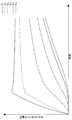
- FIG. 3 shows an output voltage (upper) and a capacitor voltage curve (lower) when the capacitor module is discharged using this apparatus.
- FIG. 3 shows an output voltage (upper) and a capacitor voltage curve (lower) when the capacitor module is discharged using this apparatus.
- FIG. 3 shows an output voltage (upper) and a capacitor voltage curve (lower) when the capacitor module is discharged using this apparatus.
- FIG. 3 shows an output voltage (upper) and a capacitor voltage curve (lower) when the capacitor module is discharged using this apparatus.
- an object is to provide a method for uniformly using a power storage bank in charge and discharge. Another object is to suppress fluctuations in the input voltage from the charger or the output voltage to the load within an arbitrary range while uniformly using the power storage bank in charging and discharging.
- a power storage module in which a plurality of power storage units composed of one power storage bank or a plurality of power storage banks connected in series are connected in series, and charging for charging the power storage bank , A balance circuit that is connected to the power storage module and corrects variation in the charge / discharge state of the power storage bank, and a voltage detection unit that detects one or more voltages of the power storage bank and / or the voltage of the charger A plurality of taps taken out from each of one or more series connection points of one terminal of the power storage module and / or the plurality of power storage units via a switch, and one of the plurality of taps is the A switch control unit that switches the switch so that the switch is connected to one terminal of the charger, and the switch control unit proceeds with charging during the charging period. Accordingly, the switches are sequentially switched based on the detection result of the voltage detection unit so as to control the number of the plurality of power storage units that are directly charged from the charger without going through the balance circuit.
- a power storage module in which a plurality of power storage units
- a power storage module in which a plurality of power storage units composed of a single power storage bank or a plurality of power storage banks connected in series are connected in series, and charging for charging the power storage bank ,
- a balance circuit that is connected to the power storage module and corrects variation in the charge / discharge state of the power storage bank, and a voltage detection unit that detects one or more voltages of the power storage bank and / or the voltage of the charger
- a plurality of taps taken out via a switch from one or more of the one terminal of the power storage module and / or the other terminal of the power storage module and / or the series connection point of the plurality of power storage units, Switch control for switching the switch so that one of the plurality of taps is connected to one terminal or the other terminal of the charger.
- the switch control unit is directly charged from the charger without going through the balance circuit based on the detection result of the voltage detection unit according to the progress of charging during the charging period.
- the power storage system is characterized in that the switches are sequentially switched so as to control the number of power storage units.
- the plurality of power storage units are grouped into a plurality of groups, and charging is progressed in a time-sharing manner for each of the plurality of groups. Accordingly, the switches are sequentially switched based on the detection result of the voltage detection unit so as to control the number of the plurality of power storage units that are directly charged from the charger without going through the balance circuit.
- the switch control unit detects the voltage detection unit according to the progress of charging in a time-sharing manner with respect to each of the plurality of groups in which the plurality of power storage units are grouped into a plurality of groups. Based on the result, the switches are sequentially switched so as to control the number of the plurality of power storage units that are directly charged from the charger without going through the balance circuit.
- the switch control unit further regroups the plurality of power storage units into a group larger than the number of groups of the power storage units after the predetermined number of times of switch switching. Directly from the charger without passing through the balance circuit based on the detection result of the voltage detection unit according to the progress of charging in a time-sharing manner for each of the groups larger than the number of groups of the power storage units. One or more of the switches are sequentially switched so as to control the number of the plurality of power storage units to be charged.
- a power storage module in which a plurality of power storage units composed of one power storage bank or a plurality of power storage banks connected in series are connected in series, and a load supplied with power from the power storage bank
- a balance circuit that is connected to the power storage module and corrects variation in the charge / discharge state of the power storage bank, and detects one or more voltages of the power storage bank and / or a discharge voltage from the power storage bank to the load.
- a plurality of taps taken out from each of one or more series connection points of one of the terminals of the power storage module and / or the plurality of power storage units via a switch, and the plurality of taps A switch control unit that switches the switch so that one of the switches is connected to one terminal of the load, the switch control unit,
- the number of the plurality of power storage units that are discharged directly from the power storage bank to the load without going through the balance circuit is controlled based on a detection result of the voltage detection unit according to a discharge state during a power supply period. It is an object of the present invention to provide a power storage system characterized by sequentially switching the switches.
- a power storage module in which a plurality of power storage units composed of one power storage bank or a plurality of power storage banks connected in series are connected in series, and a load supplied with power from the power storage bank
- a balance circuit that is connected to the power storage module and corrects variation in the charge / discharge state of the power storage bank, and detects one or more voltages of the power storage bank and / or a discharge voltage from the power storage bank to the load.
- a plurality of voltage detection units to be taken out from one or more of the one terminal of the power storage module and / or the other terminal of the power storage module and / or one or more series connection points of the plurality of power storage units via a switch.
- the switch control unit is configured such that the plurality of power storage units are grouped into a plurality of groups, and each of the plurality of groups is time-divisionally and the detection result of the voltage detection unit according to a discharge state
- the switches are sequentially switched so as to control the number of the plurality of power storage units that are directly discharged from the load without going through the balance circuit.
- the switch control unit further regroups the plurality of power storage units into a group smaller than the number of groups of the power storage units after the predetermined number of times of switch switching.
- the switch control unit In a time-sharing manner with respect to each of the groups smaller than the number of groups of the power storage units, according to the discharge state, based on the detection result of the voltage detection unit, directly from the power storage module without passing through the balance circuit
- One or more of the switches are sequentially switched so as to control the number of the plurality of power storage units discharged to the load.
- a power storage module in which a plurality of power storage units composed of one power storage bank or a plurality of power storage banks connected in series are connected in series, and charging for charging the power storage bank ,
- a balance circuit that is connected to the power storage module and corrects variation in the charge / discharge state of the power storage bank, and a voltage detection unit that detects one or more voltages of the power storage bank and / or the voltage of the charger
- a power storage system wherein the switch is switched at least once based on a detection result of a detection unit so as to reduce the number of the plurality of power storage units that are directly charged from the charger without going
- a power storage module in which a plurality of power storage units composed of one power storage bank or a plurality of power storage banks connected in series are connected in series, and charging for charging the power storage bank ,
- a balance circuit that is connected to the power storage module and corrects variation in the charge / discharge state of the power storage bank, and a voltage detection unit that detects one or more voltages of the power storage bank and / or the voltage of the charger
- a plurality of taps taken out via a switch from one or more of the one terminal of the power storage module and / or the other terminal of the power storage module and / or the series connection point of the plurality of power storage units, Switch control for switching the switch so that one of the plurality of taps is connected to one terminal or the other terminal of the charger.
- the switch control unit reduces the number of the plurality of power storage units that are directly charged from the charger without going through the balance circuit based on a detection result of the voltage detection unit during a charging period.
- the power storage system is characterized in that the switch is switched at least once.
- the switch control unit further includes the voltage detection unit in a time-sharing manner for each of the plurality of groups in which the plurality of power storage units are grouped into a plurality of groups after a predetermined number of times of switch switching. Based on the detection result, the switch is switched at least once so that the number of the plurality of power storage units that are directly charged from the charger without going through the balance circuit is reduced.
- the switch control unit is configured to perform the charging based on a detection result of the voltage detection unit in a time-sharing manner for each of the plurality of groups in which the plurality of power storage units are grouped into a plurality of groups.
- the switch is switched at least once so that the number of the plurality of power storage units that are directly charged from the battery without going through the balance circuit is reduced.
- the switch control unit further regroups the plurality of power storage units into a group larger than the number of groups of the power storage units after the predetermined number of times of switch switching.
- the plurality of power storage units that are charged directly from the charger without passing through the balance circuit based on the detection result of the voltage detection unit in a time-sharing manner for each of the groups that are larger than the number of groups of the power storage units.
- One or more switching of the switch is performed at least once to reduce the number of units.
- a power storage module in which a plurality of power storage units composed of one power storage bank or a plurality of power storage banks connected in series are connected in series, and a load supplied with power from the power storage bank
- a balance circuit that is connected to the power storage module and corrects variation in the charge / discharge state of the power storage bank, and detects one or more voltages of the power storage bank and / or a discharge voltage from the power storage bank to the load.
- a plurality of taps taken out from each of one or more series connection points of one of the terminals of the power storage module and / or the plurality of power storage units via a switch, and the plurality of taps A switch control unit that switches the switch so that one of the switches is connected to one terminal of the load, the switch control unit, Based on the detection result of the voltage detection unit, the switch is switched at least once so that the number of the power storage units that are discharged directly from the power storage bank to the load without going through the balance circuit is increased during a power supply period.
- a power storage module in which a plurality of power storage units composed of a single power storage bank or a plurality of power storage banks connected in series are connected in series, and a load supplied with power from the power storage bank
- a balance circuit that is connected to the power storage module and corrects variation in the charge / discharge state of the power storage bank, and detects one or more voltages of the power storage bank and / or a discharge voltage from the power storage bank to the load.
- a plurality of voltage detection units to be taken out from one or more of the one terminal of the power storage module and / or the other terminal of the power storage module and / or one or more series connection points of the plurality of power storage units via a switch.
- a switch control unit for switching wherein the switch control unit discharges directly from the power storage bank to the load without passing through the balance circuit based on a detection result of the voltage detection unit during a discharge period.
- the power storage system is characterized in that the switch is switched at least once so that the number of switches increases.
- the switch control unit is configured to perform the charging based on a detection result of the voltage detection unit in a time-sharing manner for each of the plurality of groups in which the plurality of power storage units are grouped into a plurality of groups.
- the switch is switched at least once so that the number of the power storage units that are directly discharged from the vessel without going through the balance circuit is increased.
- the switch control unit further regroups the plurality of power storage units into a group smaller than the number of groups of the power storage units after the predetermined number of times of switch switching. Based on the detection result of the voltage detection unit, each of the groups smaller than the number of groups of the power storage units is discharged directly from the power storage module to the load without passing through the balance circuit. The switch is switched at least once so that the number of power storage units increases.
- a power storage module in which a plurality of power storage units composed of one power storage bank or a plurality of power storage banks connected in series are connected in series, and charging for charging the power storage bank ,
- a balance circuit that is connected to the power storage module and corrects variation in the charge / discharge state of the power storage bank, and a voltage detection unit that detects one or more voltages of the power storage bank and / or the voltage of the charger
- a plurality of taps taken out via a switch from one or more of the one terminal of the power storage module and / or the other terminal of the power storage module and / or the series connection point of the plurality of power storage units, Switch control for switching the switch so that one of the plurality of taps is connected to one terminal or the other terminal of the charger.
- the switch control unit is configured such that the plurality of power storage units are grouped into a plurality of groups, and the same power storage unit for each of the plurality of groups without the balance circuit from the charger. It is an object of the present invention to provide a power storage system in which the switches are sequentially switched so that direct charging is repeatedly performed in a time division manner.
- a power storage module in which a plurality of power storage units composed of a single power storage bank or a plurality of power storage banks connected in series are connected in series, and a load supplied with power from the power storage bank
- a balance circuit that is connected to the power storage module and corrects variation in the charge / discharge state of the power storage bank, and detects one or more voltages of the power storage bank and / or a discharge voltage from the power storage bank to the load.
- a plurality of voltage detection units to be taken out from one or more of the one terminal of the power storage module and / or the other terminal of the power storage module and / or one or more series connection points of the plurality of power storage units via a switch.
- a switch control unit for switching wherein the plurality of power storage units are grouped into a plurality of groups, and for each of the plurality of groups, the same power storage unit performs direct discharge to a load in a time-sharing manner. It is an object of the present invention to provide a power storage system in which the switches are sequentially switched so as to be repeatedly performed.
- the power storage system according to the present invention efficiently balances power storage banks even when only a balance circuit that corrects variations in charge / discharge states due to the effects of the internal resistance of the power storage bank and the characteristics of the balance circuit requires time for correction. Can be done automatically.
- the power storage system appropriately selects the tap connected to the charger and the load according to the voltage value of the power storage bank and / or the charger, while maintaining the voltage of the power storage bank uniform,
- the charging voltage from the charger and the discharging voltage to the load can be suppressed within a certain range without using a DC-DC converter or the like.
- FIG. 1 It is a circuit diagram of the conventional capacitor power supply device. It is a circuit diagram of the conventional capacitor power supply device. It is the graph which showed the output voltage (upper) at the time of discharging a capacitor module using the capacitor power supply device shown in FIG. 2, and the voltage curve (lower) of a capacitor. It is a circuit diagram of the electrical storage system which concerns on Example 1 of this invention. It is the charger voltage (upper) at the time of charging in the electrical storage system which concerns on Example 1, and the charge curve (lower) of a capacitor bank. It is a circuit diagram of the electrical storage system which concerns on Example 2 of this invention. FIG.
- Example 6 is an example of a charging waveform of a part of the capacitor banks when the capacitor module is charged using a balance circuit that has a limited equalization ability in the power storage system according to the first embodiment.
- It is a circuit diagram of the electrical storage system which concerns on Example 3 of this invention.
- It is a circuit diagram of the electrical storage system which concerns on Example 4 of this invention.
- It is a diagram showing a state in which by selecting the S 39a and S 13b in Example 4 is charging.
- Example 4 it is a figure which shows the state in which the capacitor units grouped into 2 groups are charged by the time division.
- FIG. 10 is an example of a charging waveform of a part of capacitor banks when the capacitor module is charged using a balance circuit having a limited equalization ability in the power storage system according to the fourth embodiment.
- FIG. 10 is an example of a charging waveform of a part of capacitor banks when the capacitor module is charged using a balance circuit having a limited equalization ability in the power storage system according to the fourth embodiment.
- It is a circuit diagram of the electrical storage system which concerns on the modification of Example 4 of this invention.
- It is a circuit diagram of the electrical storage system which concerns on Example 5 of this invention.
- FIG. 10 is an example of a charging waveform of a part of capacitor banks when the capacitor module is charged using a balance circuit having a limited equalization ability in the power storage system according to the fourth embodiment.
- Example 9 shows a load voltage (upper) and a discharge curve (lower) of a capacitor bank when discharging is performed in the power storage system according to the fifth embodiment. It is a circuit diagram of the electrical storage system which concerns on Example 6 of this invention. It is a circuit diagram of the electrical storage system which concerns on Example 7 of this invention. It is a circuit diagram of the electrical storage system which concerns on Example 8 of this invention. It is a figure which shows the state which the capacitor unit grouped into 4 groups in Example 8 is discharging by time division. In Example 8, it is a figure which shows the state in which the capacitor unit grouped into 3 groups is discharging by time division. It is a diagram showing a state of performing discharge by selecting the S 39a and S 13b in example 8.
- a “capacitor bank” refers to a single capacitor cell or a capacitor cell that is configured by series, parallel, or series-parallel connection of a plurality of capacitor cells
- a “capacitor unit” refers to a single capacitor cell.
- a capacitor bank or a plurality of capacitor banks connected in series is referred to, and a “capacitor module” refers to a structure in which a plurality of capacitor units are connected in series.
- the “storage cell” refers to a capacitor, a secondary battery, or the like.
- Storage bank refers to a single storage cell or a plurality of storage cells configured in series, parallel, or series-parallel connection
- storage unit refers to a single storage bank or connected in series
- storage module refers to a structure in which a plurality of storage units are connected in series.
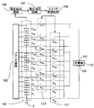
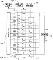
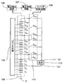
- FIG. 4 is a circuit diagram of the power storage system according to Embodiment 1 of the present invention.
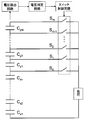
- the capacitor module 109 configured by connecting m capacitor banks of the rated voltage V c in series, n taps are provided for each capacitor unit composed of h capacitor banks, and a balance circuit 105 is provided.
- the balance circuit is a circuit for correcting variations in the charge / discharge states of the storage banks constituting the storage module, and energy transfer between the storage banks, that is, a balance operation during both charging and discharging periods. It can be performed.
- the balance circuit is roughly classified into a method using a capacitor, a method using a coil, and a method using a transformer.
- Various specific circuits are known (for example, Patent Document 2, Non-patent document 1).
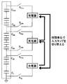
- the switches S 2a to S 51a constitute a switch group 110 and are connected between the taps taken out from the respective series connection points of the capacitor units and the high potential side terminal 101 of the charger 112. ing.
- C 1 to C 100 are capacitor banks. Any one of the switches S 2a to S 51a is on and is directly connected to the high potential side terminal 101 of the charger 112.
- the low potential side terminal 102 of the charger is fixedly connected to the ground 0 of the capacitor module.
- the voltage detection circuit 106 detects the voltages of all or some of the capacitor banks that constitute the capacitor module 109.
- the voltage detection result is compared with the reference voltage in the voltage determination circuit 107, and the switch control circuit 108 switches the switch based on the comparison result, so that the charging voltage from the charger is within an arbitrary range, for example, the charger It is controlled to be within the allowable fluctuation voltage.
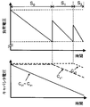
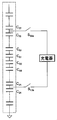
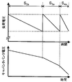
- FIG. 5 shows a charger voltage (upper) and a capacitor bank charging curve (lower) when charging is performed in the configuration of FIG.
- the operation of the balance circuit is ideal, and the description will be made on the assumption that the voltage of each capacitor bank constituting the capacitor module is kept uniform by the balance circuit under any conditions.
- the charger voltage As the charge progresses, the voltage of each capacitor bank Yuki rises, the charger voltage reaches the V in. At this time, if the voltage of each capacitor bank is uniform, the voltage of each bank is V in / 100.
- the switch control circuit 108 turns on the S 50a and simultaneously turns off the switch S 51a, which As a result, the tap connecting the charger 112 and the capacitor module 109 is shifted to the lower side by one. As a result, the charger voltage is lowered by the voltage of the capacitor banks C 100 and C 99 , that is, (2 ⁇ V in ) / 100.
- the power from the charger is supplied to the capacitor unit on the low potential side of the tap connected to S 50a , that is, the capacitor banks C 1 to C 98 are directly charged from the charger.
- the capacitor banks C 100 and C 99 are charged by receiving charges from the capacitor banks C 1 to C 98 via the balance circuit.
- the charger voltage by the voltage determination circuit 107 based on a voltage detection result by the voltage detection circuit 106 is determined to have reached again V in, the switch control circuit 108 turns off the switch S 50a simultaneously
- the tap connecting the charger 112 and the capacitor module 109 is further shifted down by one.
- the charger voltage is lowered by the voltage of the capacitor banks C 98 and C 97 , that is, (2 ⁇ V in ) / 98.
- the capacitor unit on the low potential side of the tap connected to S 49a that is, the capacitor bank of C 1 to C 96 is directly charged from the charger.
- the capacitor banks C 97 to C 100 are charged by receiving charges from the capacitor banks C 1 to C 96 via the balance circuit.
- each capacitor can be uniformly charged while keeping the charger voltage within a certain range.
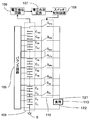
- FIG. 6 is a circuit diagram of a power storage system according to Embodiment 2 of the present invention. In the figure, parts corresponding to those in FIG.
- the high-potential side terminal 101 of the charger 112 is connected to each tap of the capacitor module 109 via the switch group 110, whereas in the present embodiment, the low-potential side of the charger 112 is connected.
- a switch group 111 including S 1b to S 50b is provided between the terminal 102 and the capacitor module 109. In this embodiment, the switches are switched in the order of S 1b , S 2b ,..., S 50b by the switch control circuit 108 based on the voltage detection result by the voltage detection circuit 106.
- the operation of the balance circuit is ideal, and the description has been made on the assumption that the voltage of each capacitor bank constituting the capacitor module is kept uniform by the balance circuit under any conditions.
- the characteristics of the balance circuit are not ideal, and variations in the voltage of the capacitor bank occur due to the limitation of the equalization capability and the presence of the equivalent series resistance of the capacitor bank.
- FIG. 7 shows an example of charging waveforms of C 15 , C 15 , C 20 and C 25 . It can be seen that the capacitor banks are not uniformly charged during the charging process.
- the capacitor banks that are not directly charged from the charger are balanced from the capacitor banks that are directly charged (capacitor banks C 1 to C 5 on the lower potential side than S 5a ). It is charged by receiving the charge via the circuit, but the balance circuit is not fast enough to transfer the charge from the low potential side to the high potential side.
- the bank is located farther from the charger, and the progress of charging becomes slower. Although the voltage of each bank eventually converges due to the function of the balance circuit, it takes a long time until the voltage of each bank is sufficiently equalized. In addition, a charge voltage overshoot phenomenon (overcharge) is observed in some capacitor banks C1.
- FIG. 8 is a circuit diagram of a power storage system according to Example 3 of the present invention. In the figure, parts corresponding to those in FIG.
- the low potential side terminal 102 of the charger and the ground 0 of the capacitor module 109 are directly connected, whereas in this embodiment, the low potential side terminal 102 is connected to the ground 0 of the capacitor module 109. Not directly connected but fixedly connected to the series connection point of the capacitor banks C2 and C3.
- the switches are switched in the order of S 51a , S 50a ,..., S 3a by the switch control circuit 108 based on the voltage detection result by the voltage detection circuit 106.
- the switch S 2a is on, the two capacitor banks C 1 and C 2 are directly charged, and the other capacitor banks are charged via the balance circuit. Yes.
- the capacitor bank of the C 100 is the most electrically separated from the charger 112 (98 banks min), when the characteristic of the balancing circuit is not ideal, would indicate a lowest voltage in the charging process.
- the low potential side terminal 102 of the charger 112 is connected to the ground 0 of the capacitor module 109.
- the low potential side terminal of the charger and the ground terminal of the capacitor module are connected to each other. In the configuration that is not directly connected, the electrical distance between the balance circuit and the capacitor bank at the end of charging can be shortened compared to the configuration of the first embodiment.
- the charger 112 since the low potential side terminal 102 of the charger is fixedly connected to the series connection point of the capacitor banks C 2 and C 3 , the charger 112 cannot directly charge the capacitor banks of C 1 and C 2. I can't. However, the capacitor banks C 1 and C 2 are charged by receiving charges from other capacitor banks via the balance circuit 105.
- the switch S 3a is turned on, the capacitor banks of C 3 and C 4 are directly charged, and the other banks are charged via the balance circuit.
- the capacitor bank of C 100 that is the most electrically separated from the charger 112 is 98 banks separated in the configuration of FIG. 4 of the first embodiment, whereas in the configuration of the present embodiment, the low charge of the charger 112 is low. Since the potential side terminal 102 is connected to the high potential side (direct connection point between C 2 and C 3 ) by two banks, 96 banks closer to the charger by two banks than the configuration of FIG. The distance in minutes. Therefore, it is possible to suppress the voltage variation of the capacitor bank to be smaller than that of the configuration of FIG.
- the high-potential side terminal 101 and the low-potential side terminal 102 of the charger 112 are respectively connected to S 27a and S 26a , or What is necessary is just to connect to S26a and S25a .
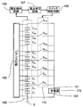
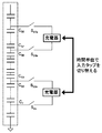
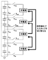
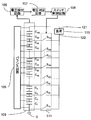
- FIG. 9 is a circuit diagram of a power storage system according to Embodiment 4 of the present invention. In the figure, parts corresponding to those in FIG.
- the high potential side terminal 101 and the low potential side terminal 102 of the charger 112 are respectively connected to the switch S. 27a and S26a or switches S26a and S25a may be connected.
- a bank a bank located on the low potential side such as C 1
- voltage variations occur even in the initial stage of charging.
- the present embodiment is not limited to this, but solves such problems.
- the switches S 2a to S 51a constitute a first switch group 110 ′, and the switches S 1b to S 50b constitute a second switch group 111 ′, and taps and charging taken out from each of the series connection points of the capacitor units.
- the high-potential side terminal 101 and the low-potential side terminal 102 are connected to each other.
- the charger voltage reaches the V in.
- the switch control circuit 108 turns on at the same time switches S 50a is turned off to switch S51a, which As a result, the tap connecting the high potential side terminal 101 of the charger 112 and the capacitor module 109 is shifted to the lower side by one.
- the capacitor banks C 1 to C 98 are directly charged by the charger without going through the balance circuit, and the capacitor banks C 99 and C 100 are charged through the balance circuit.
- the switch control circuit 108 turns off the switch S 1b simultaneously
- the switch S2b is turned on, thereby shifting the tap connecting the low potential side terminal 102 of the charger 112 and the capacitor module 109 upward by one.
- the capacitor banks C 3 to C 98 are directly charged by the charger without going through the balance circuit, and the capacitor banks C 1 , C 2 , C 99 , and C 100 are charged through the balance circuit.
- the taps connected to the high-potential side terminal 101 and the low-potential side terminal 102 of the charger are sequentially switched as the charging progresses.
- the banks (C 50 , C 51 ) near the center of the capacitor bank are set to the center of the capacitor bank that is directly charged by the charger.
- C 50 and C 51 is Yuki sequentially switches the switch such that the center of the capacitor bank is charged directly by the charger, S 39a and S 13b are selected, total 52 C 25 ⁇ C 76 of It shows a state in which the capacitor bank is directly charged by a charger (for simplicity, a balance circuit, a non-operating switch, etc. are omitted).
- the other capacitor banks C 1 to C 24 and C 77 to C 100 are charged via a balance circuit. By performing such switch switching, the electrical distance between the capacitor bank charged via the balance circuit and the charger can be made as short as possible.
- the capacitor bank of the capacitor module 109 is changed to m ⁇ 1 / 4, m ⁇ 3/4, that is, grouped into two groups so that the banks around C 25 and C 75 are the center of the series-connected capacitor banks that are directly charged by the charger.
- the switch control circuit 108 selects a switch and performs charging by a charger in a time division manner.
- the switch control circuit 108 selects the switches S 47a and S 29b and the switches S 22a and S 4b so that the bank around C 25 and C 75 is the center of the series-connected capacitor bank that is directly charged by the charger.
- a capacitor bank of C 57 to C 92 and a capacitor bank of C 7 to C 42 are alternately directly charged by a charger in a time division manner.
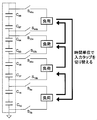
- the capacitor bank of the capacitor module 109 So that the banks around m ⁇ 1/6, m ⁇ 3/6, m ⁇ 5/6, that is, C 17 , C 50 , C 83 are the center of the series-connected capacitor banks that are directly charged by the charger.
- the switches are grouped into three groups, and the switch control circuit 108 selects a switch for each of the three groups thus grouped, and performs charging by a charger in a time division manner. In FIG.
- the switch control circuit 108 selects the switches S 51a and S 35b , the switches S 34a and S 18b , and the switches S 17a and S 1b , and C 69 to C 100 , C 35 to C 66 and C 1 to C 32 are selected. This shows a state where the capacitor banks are directly charged by the charger alternately.
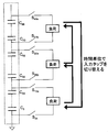
- the capacitor bank of the capacitor module 109 is m ⁇ 1/8, m ⁇ 3/8, m ⁇ 5/8, m ⁇ 7/8, that is, series connected capacitors in which banks around C 13 , C 38 , C 63 , C 88 are directly charged by a charger
- the four groups are grouped so as to be the center of the bank, and the switch control circuit 108 selects a switch for each of the four groups thus grouped, and performs charging by a charger in a time division manner.
- switch control circuit 108 switches S 48a and S 42b, switches S 35a and S 29 b, switches S 23a and S 17b, and select switches S 10a and S 4b, C 83 ⁇ C 94 , C 57 ⁇ C 68 shows a state in which capacitor banks of C 33 to C 44 and C 7 to C 18 are alternately charged directly by a charger.
- any grouped charging stage it is desirable to switch the switches so that the time for which each capacitor unit is directly charged by the charger is equal from the viewpoint of keeping the voltage of each capacitor bank as uniform as possible.
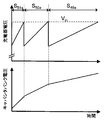
- FIG. 14A shows an example of charging waveforms of some capacitor banks C 1 , C 5 , C 10 , C 15 , C 20 , and C 25 in the case where a balance circuit having a limitation is used. It can be seen that the charge waveforms of the capacitor banks are in good agreement, and the capacitor banks are charged uniformly. It can also be seen that the charging time of each capacitor bank is short. Compared with FIG. 7 of the example of Example 1, it can be seen that the improvement is made significantly.
- charging is started from a state where a plurality of power storage banks constituting the power storage module is not grouped, but charging is started from a state where a plurality of power storage banks constituting the power storage module are grouped. You can also.
- the switch is switched so that the number of capacitor units directly charged by the charger is reduced.
- the same capacitor unit is directly charged by the charger for each of the plurality of groups. Even in a configuration in which these are repeatedly performed in a time-sharing manner, the electrical distance to the capacitor unit charged through the balance circuit can be shortened, so that charging to each capacitor bank can be performed more evenly.
- the layout of the position and number of switches is such that one of the plurality of taps is connected to one terminal or the other terminal of the charger, and without a balance circuit from the charger.
- the configuration can be changed as appropriate as long as the switch can be sequentially switched so as to control the number of the plurality of power storage units that are directly charged.
- the one shown in FIG. 15 can be considered.
- the number of power storage units that are directly charged from the charger is increased in the charging process. It is also conceivable to switch the switch as described above. Therefore, based on the voltage detection result by the voltage detection circuit, it is conceivable to appropriately combine switching of switches such that the number of power storage units directly charged from the charger is reduced, made constant, or increased.
- the configuration of the storage unit where charging starts the number of groups in each grouping stage of the plurality of storage banks constituting the storage module, the number of storage banks in each group, and the like can be arbitrarily selected. it can.
- the timing of the switch by the switch control circuit 108 although the charger voltage based on a voltage detection result by the voltage detection circuit 106 was when it is determined to have reached the V in, the charger voltage to which the voltage is determined to have reached can be any voltage less than V in.
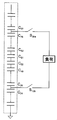
- FIG. 16 is a circuit diagram of a power storage system according to Example 5 of the present invention. In the figure, parts corresponding to those in FIG.
- the configuration of the present embodiment is obtained by replacing the charger in the configuration of the first embodiment with the load 113, and basically performing an operation reverse to that during charging (switch switching order, etc.) to output It is possible to discharge each capacitor bank uniformly while suppressing voltage fluctuation.
- FIG. 17 shows operation waveforms when discharging is performed with the configuration of FIG. Contrary to the charging operation described with reference to FIGS. 4 to 5 of the first embodiment, the voltage determination circuit 107 determines the load voltage detected by the voltage detection circuit 106 by starting from the state where S2a is on.
- the switch control circuit 108 suppresses the load voltage within a certain range by sequentially switching the switch to the upper side so that the load voltage does not fall below a certain arbitrary value (for example, the allowable lower limit voltage V low of the load).
- the capacitor bank directly connected to the load (C 1 and C 2 when S 2a is on) discharges directly to the load, and the other capacitor banks discharge through the balance circuit.
- FIG. 18 is a circuit diagram of a power storage system according to Embodiment 6 of the present invention.
- parts corresponding to those in FIG. 16 are denoted by the same reference numerals, and description of parts similar to those in the fifth embodiment is omitted.
- the switch group 110 is provided between the high-potential side terminal 121 of the load 113 and the capacitor module 109, whereas in the present embodiment, the switch group 110 is provided between the low-potential side terminal 122 and the capacitor module 109.
- a switch group 111 is provided. In this embodiment, the switches are switched in the order of S 50b , S 49b ,..., S 1b by the switch control circuit 108 based on the voltage detection result by the voltage detection circuit 106.
- FIG. 19 is a circuit diagram of a power storage system according to Example 7 of the present invention.
- parts corresponding to those in FIG. 16 are denoted by the same reference numerals, and description of parts similar to those in the fifth embodiment is omitted.
- the low potential side terminal 122 of the load 113 and the ground 0 of the capacitor module 109 are directly connected, whereas in this embodiment, the low potential side terminal 122 is connected to the ground 0 of the capacitor module 109. And is fixedly connected to the series connection point of the capacitor banks C 2 and C 3 .
- the switch is switched in the order of S 3a , S 4a ,..., S 51a by the switch control circuit 108 based on the voltage detection result by the voltage detection circuit 106.
- the low potential side terminal 122 of the load 113 is connected to the ground 0 of the capacitor module 109.
- the low potential side terminal of the load and the ground terminal of the capacitor module are directly connected.
- the switch S 3a is turned on, and the capacitor banks C 3 and C 4 are directly discharged to the load, and the capacitor banks C 1 , C 2 , C 5 to C 100 are balanced. Discharging occurs through the circuit.
- the capacitor bank of C 100 that is the most electrically separated from the load 113 was separated by 98 banks in the fifth embodiment, whereas the low potential side terminal 122 of the load 113 has two banks in the configuration of the present embodiment. Since it is connected to the high potential side (the direct connection point between C 2 and C 3 ), it is a distance of 96 banks that is closer to the charger by 2 banks than the configuration of the fifth embodiment. Therefore, it is possible to suppress the voltage variation of the capacitor bank to be smaller in the initial stage of the discharging process than in the case of the fifth embodiment.
- the high potential side terminal 121 and the low potential side terminal 122 of the load 113 are respectively connected to the switches S 27a and S 26a , or What is necessary is just to connect to switch S26a and S25a .
- FIG. 20 is a circuit diagram of a power storage system according to Example 8 of the present invention.
- parts corresponding to those in FIG. 16 are denoted by the same reference numerals, and description of parts similar to those in the fifth embodiment is omitted.
- the configuration of the present embodiment is obtained by replacing the charger in the configuration of the fourth embodiment with a load 113, and basically an operation reverse to that during charging (switch switching order, capacitor bank grouping order, etc.) By performing the above, it is possible to uniformly discharge each capacitor bank while suppressing output voltage fluctuation.
- m capacitor banks of rated voltage Vc are connected in series, and n taps (each composed of n switches) are provided for each capacitor unit composed of h banks.
- the switches S 2a to S 51a constitute a first switch group 110 ′, and the switches S 1b to S 50b constitute a second switch group 111 ′, and taps and loads taken out from the respective series connection points of the capacitor units. 113 is connected between the high potential side terminal 121 and the low potential side terminal 122.
- the present embodiment basically performs an operation opposite to that of the fourth embodiment, which is an embodiment during charging. Therefore, here, as an example, a description will be given of a state in which the number of groups at the start of discharge is four, that is, a configuration in which the capacitor banks constituting the capacitor module are grouped into four groups.
- the capacitor bank of the capacitor module 109 is set to m ⁇ 1/8, m ⁇ 3/8, m ⁇ 5/8, m ⁇ 7/8, that is, C 13 , C 38 , C 63 , C
- the group is divided into four groups so that the bank around 88 is the center of the series-connected capacitor bank that discharges directly to the load.
- the switch control circuit 108 configures each group. Select the switch so that the banks near the center of the series-connected capacitor banks (banks per C 13 , C 38 , C 63 , C 88 ) become the center of the series-connected capacitor bank group that discharges directly to the load, and time division To discharge to the load.
- the switch control circuit 108 selects the switches S 8a and S 7b , S 20a and S 19b , S 33a and S 32b , S 45a and S 44b , and C 13 to C 14 , C 37 to C 38 , C
- a state is shown in which capacitor banks 63 to C 64 and C 87 to C 88 are alternately discharged to the load.
- the operation of the four in each group will be described taking the group containing the capacitor bank C 13 as an example. First, start from a state where S 8a and S 7b are on.
- the voltage of each capacitor bank decreases, and based on the voltage detection result by the voltage detection circuit 106, the voltage determination circuit 107 determines that the load voltage has reached the allowable lower limit voltage V low of the load.
- the switch control circuit 108 when the switch is turned off S 8a turns on the switch S 9a simultaneously, thereby shifting the tap for connecting the high-potential side terminal 121 and the capacitor module 109 of the load 113 to one minute upper side.
- the capacitor banks C 13 to C 16 are discharged directly to the load without going through the balance circuit, and the other capacitor banks are discharged through the balance circuit.
- the switch control circuit 108 turns off the switch S7b and simultaneously switches the switch S7b.
- the tap connecting the low potential side terminal 122 of the load 113 and the capacitor module 109 is shifted to the lower side by one.
- the capacitor banks C 11 to C 16 are discharged directly to the load without passing through the balance circuit, and the other capacitor banks are discharged via the balance circuit.
- the capacitor bank of the capacitor module 109 3 ⁇ 3/6, m ⁇ 3/6, m ⁇ 5/6, that is, the capacitor bank around C 17 , C 50 , and C 83 is the center of the series-connected capacitor bank that discharges directly to the load.
- the switch control circuit 108 includes a bank (around C 17 , C 50 , C 83) near the center of the series-connected capacitor banks that constitute each group.
- the switch control circuit 108 selects the switches S 15a and S 3b , the switches S 32a and S 20b , and the switches S 49a and S 37b , and C 5 -C 28 , C 39 -C 62 , C 73 This shows a state in which the capacitor banks of .about.C 96 alternately discharge directly to the load. Since the switch control by the switch control circuit 108 in each group is the same as described above, the description thereof is omitted.
- FIG. 23 shows a state in which the switches S 39a and S 13b are selected, the capacitor banks C 25 to C 76 are discharged directly to the load, and the other banks are discharged via the balance circuit. Assuming that the voltage of the capacitor bank at the time of discharge is V dis , the above grouped discharge is repeated until m ⁇ V dis ⁇ V low is satisfied. By repeating the above operation, the discharge from each capacitor bank is performed more evenly, and as a result, the discharge time can be prolonged.
- any grouped discharge stage it is desirable to switch the switches so that the time for each capacitor bank to discharge directly to the load is equal from the viewpoint of keeping the voltage of each capacitor bank as uniform as possible.
- switching is performed so that the number of capacitor units directly discharged to the load is increased.
- the same capacitor unit repeatedly performs direct discharge to the load in a time division manner for each of a plurality of groups. Even in the configuration, since the electrical distance to the capacitor unit discharged via the balance circuit can be shortened, the discharge from each capacitor bank can be performed more evenly.
- the layout of the position and number of switches is such that one of the plurality of taps is connected to one terminal of the load or the other terminal, and the balance circuit is provided. Any configuration can be used as long as the switches can be sequentially switched so as to control the number of the plurality of power storage units that are directly discharged to the load without intervention.
- the number of power storage units that directly discharge to the load in the discharging process It is also conceivable to switch the switches so as to reduce the number of switches. Therefore, based on the voltage detection result by the voltage detection circuit, it is conceivable to appropriately combine switching of switches such that the number of power storage units directly discharged to the load is reduced, made constant, or increased.
- the configuration of the storage unit starting discharge, the number of groups in each grouping stage of the plurality of storage banks constituting the storage module, the number of storage banks in each group, and the like can be arbitrarily selected. it can.
- the switch switching timing by the switch control circuit 108 is when it is determined that the load has reached V low based on the voltage detection result by the voltage detection circuit 106, but the load voltage is The voltage determined to have reached can be any voltage greater than V low and less than the allowable upper limit voltage of the load.
- the voltage detection circuit 106 detects the voltage of each capacitor bank constituting the capacitor module 109, compares the detection result with the reference voltage in the voltage determination circuit 107, and performs switch control based on the comparison result.
- the case has been described in which the switch is switched by the circuit 108 to control the charging voltage from the charger or the discharging voltage to the load within a certain range.
- the charging voltage from the charger or the discharging voltage to the load may be detected, and switch switching control may be performed based on the detection result. .
- the capacitor bank voltage, the charging voltage from the charger, and the discharging voltage to the load show the same tendency as the characteristics described so far.
- the configuration in which n taps are provided for each capacitor unit composed of h capacitor banks has been described.
- the number of capacitor banks constituting the capacitor unit (the interval at which taps are provided) is set at a certain position. Then, it may be arbitrarily changed depending on the position, such as h, and a certain position is h + 1.
- the rated voltage of each capacitor bank is V c , but the rated voltage is arbitrarily changed depending on each capacitor bank, such as Vc ′ for a certain capacitor bank and V c ′′ for a certain capacitor bank. May be.
- the present invention can be applied to the case where another type of storage bank such as a secondary battery is used.
Landscapes
- Engineering & Computer Science (AREA)
- Power Engineering (AREA)
- Manufacturing & Machinery (AREA)
- Chemical & Material Sciences (AREA)
- Chemical Kinetics & Catalysis (AREA)
- Electrochemistry (AREA)
- General Chemical & Material Sciences (AREA)
- Charge And Discharge Circuits For Batteries Or The Like (AREA)
- Secondary Cells (AREA)
Priority Applications (4)
| Application Number | Priority Date | Filing Date | Title |
|---|---|---|---|
| CN201080039577.3A CN102577016B (zh) | 2009-09-02 | 2010-09-02 | 具有平衡电路的蓄电器件 |
| KR1020127005537A KR101726901B1 (ko) | 2009-09-02 | 2010-09-02 | 밸런스회로를 구비한 축전장치 |
| EP10813776.1A EP2475067B1 (en) | 2009-09-02 | 2010-09-02 | Electricity-storage device provided with balancing circuit |
| US13/411,480 US9318779B2 (en) | 2009-09-02 | 2012-03-02 | Electric energy storage units connected in series and selectively charged/discharged via a balancing circuit or directly from a charger or to a load |
Applications Claiming Priority (2)
| Application Number | Priority Date | Filing Date | Title |
|---|---|---|---|
| JP2009202684A JP5440918B2 (ja) | 2009-09-02 | 2009-09-02 | バランス回路を備えた蓄電装置 |
| JP2009-202684 | 2009-09-02 |
Related Child Applications (1)
| Application Number | Title | Priority Date | Filing Date |
|---|---|---|---|
| US13/411,480 Continuation US9318779B2 (en) | 2009-09-02 | 2012-03-02 | Electric energy storage units connected in series and selectively charged/discharged via a balancing circuit or directly from a charger or to a load |
Publications (1)
| Publication Number | Publication Date |
|---|---|
| WO2011027828A1 true WO2011027828A1 (ja) | 2011-03-10 |
Family
ID=43649362
Family Applications (1)
| Application Number | Title | Priority Date | Filing Date |
|---|---|---|---|
| PCT/JP2010/065041 Ceased WO2011027828A1 (ja) | 2009-09-02 | 2010-09-02 | バランス回路を備えた蓄電装置 |
Country Status (7)
| Country | Link |
|---|---|
| US (1) | US9318779B2 (enExample) |
| EP (1) | EP2475067B1 (enExample) |
| JP (1) | JP5440918B2 (enExample) |
| KR (1) | KR101726901B1 (enExample) |
| CN (1) | CN102577016B (enExample) |
| TW (1) | TWI499162B (enExample) |
| WO (1) | WO2011027828A1 (enExample) |
Cited By (1)
| Publication number | Priority date | Publication date | Assignee | Title |
|---|---|---|---|---|
| WO2020049824A1 (ja) * | 2018-09-07 | 2020-03-12 | Fdk株式会社 | 蓄電装置及び充電方法 |
Families Citing this family (26)
| Publication number | Priority date | Publication date | Assignee | Title |
|---|---|---|---|---|
| JP5440918B2 (ja) | 2009-09-02 | 2014-03-12 | 独立行政法人 宇宙航空研究開発機構 | バランス回路を備えた蓄電装置 |
| JP4590520B1 (ja) | 2009-09-02 | 2010-12-01 | 日本蓄電器工業株式会社 | 交流出力可能な蓄電装置 |
| EP2610998A4 (en) * | 2011-03-18 | 2015-07-29 | Asahi Kasei Microdevices Corp | SWITCHING OF SERIAL MEMORY CELLS AND METHOD OF COMPARING SERIAL MEMORY CELLS |
| DE102012209657A1 (de) * | 2012-06-08 | 2013-12-12 | Robert Bosch Gmbh | Verfahren und Vorrichtung zur Ermittlung des Innenwiderstandes von Batteriezellen einer Batterie |
| JP6034602B2 (ja) * | 2012-07-02 | 2016-11-30 | ローム株式会社 | 制御回路、キャパシタモジュール、電池モジュール、電源回路、それらを用いた家庭用蓄電池および車両 |
| JP6134520B2 (ja) * | 2013-01-25 | 2017-05-24 | Fdk株式会社 | バランス補正装置及び蓄電装置 |
| JP6196466B2 (ja) | 2013-05-10 | 2017-09-13 | Fdk株式会社 | 電源装置 |
| FR3019217B1 (fr) * | 2014-03-27 | 2018-07-27 | Safran Helicopter Engines | Procede et systeme de reactivation rapide de turbomachine |
| US20160105044A1 (en) * | 2014-10-08 | 2016-04-14 | Panasonic Intellectual Property Management Co., Ltd. | Power-storage-system control method and power-storage-system control apparatus |
| EP3026750A1 (de) * | 2014-11-28 | 2016-06-01 | Siemens Aktiengesellschaft | Verfahren zum Symmetrieren eines Energiespeichersystems |
| US9912164B2 (en) * | 2014-12-24 | 2018-03-06 | Intel Corporation | Multisource power delivery system |
| WO2016209698A1 (en) * | 2015-06-26 | 2016-12-29 | Amber Kinetics, Inc. | Switching fabric for energy storage and power conversion |
| CN107294145A (zh) * | 2016-03-30 | 2017-10-24 | 通用电气公司 | 充电装置、系统和方法 |
| KR101837548B1 (ko) * | 2016-04-07 | 2018-04-26 | 삼화콘덴서공업 주식회사 | 커패시터 관리 시스템 |
| JP6883396B2 (ja) * | 2016-08-25 | 2021-06-09 | 矢崎総業株式会社 | 急速充電装置 |
| DE102016122444A1 (de) * | 2016-11-22 | 2018-05-24 | HELLA GmbH & Co. KGaA | Zweispannungsbatterie |
| EP3340412B1 (de) * | 2016-12-21 | 2019-03-06 | Airbus Defence and Space GmbH | Energieversorgungsschaltung, elektrisches antriebssystem und flugkörper mit einem elektrischen antriebssystem |
| US10822858B2 (en) * | 2017-07-24 | 2020-11-03 | Gmi Holdings, Inc. | Power supply for movable barrier opener with brushless DC motor |
| JP6928347B2 (ja) * | 2017-08-02 | 2021-09-01 | NExT−e Solutions株式会社 | 管理装置、蓄電装置、蓄電システム、及び、電気機器 |
| CN107591818B (zh) * | 2017-08-11 | 2020-06-26 | 烟台海珐电气科技有限公司 | 一种解决低负载无功过补、欠补问题的无功补偿方法 |
| JP7009915B2 (ja) * | 2017-10-27 | 2022-01-26 | 株式会社デンソー | 蓄電システム |
| US10444295B2 (en) * | 2017-12-20 | 2019-10-15 | National Chung Shan Institute Of Science And Technology | Battery balance management circuit |
| CN111971871B (zh) * | 2018-03-28 | 2024-04-30 | 松下知识产权经营株式会社 | 蓄电设备用的放电电路、蓄电系统以及具备其的车辆 |
| FR3085540B1 (fr) * | 2018-08-31 | 2020-09-25 | St Microelectronics Rousset | Dispositif integre de mesure temporelle a constante de temps ultra longue et procede de fabrication |
| CN114430673A (zh) * | 2019-09-27 | 2022-05-03 | 波士顿科学医学有限公司 | 用于控制激光脉冲发生的系统和方法 |
| KR102366121B1 (ko) * | 2020-04-02 | 2022-02-22 | 엘지전자 주식회사 | 전기자동차 충전장치 |
Citations (6)
| Publication number | Priority date | Publication date | Assignee | Title |
|---|---|---|---|---|
| JPH02123928A (ja) * | 1988-10-31 | 1990-05-11 | Mitsubishi Metal Corp | 電源装置 |
| JPH08182212A (ja) * | 1994-12-26 | 1996-07-12 | Nissan Motor Co Ltd | 組電池充電制御回路 |
| JPH1032936A (ja) * | 1996-07-12 | 1998-02-03 | Tokyo R & D:Kk | 電源装置の制御システムおよび制御方法 |
| JP2000209775A (ja) | 1999-01-18 | 2000-07-28 | Okamura Kenkyusho:Kk | 直列接続段数切り換え式キャパシタ電源装置 |
| JP2003134686A (ja) * | 2001-10-23 | 2003-05-09 | Japan Storage Battery Co Ltd | 充電装置 |
| JP2008219964A (ja) | 2007-02-28 | 2008-09-18 | Japan Aerospace Exploration Agency | 蓄電モジュール |
Family Cites Families (27)
| Publication number | Priority date | Publication date | Assignee | Title |
|---|---|---|---|---|
| US3100851A (en) | 1959-11-03 | 1963-08-13 | Ling Temco Vought Inc | High power synthetic waveform generator |
| FR2418977A1 (fr) | 1978-03-02 | 1979-09-28 | Labo Electronique Physique | Onduleur universel |
| CN1022529C (zh) | 1990-06-06 | 1993-10-20 | 北京理工大学 | 高频开关电容型逆变器 |
| JPH07115728A (ja) | 1992-08-28 | 1995-05-02 | Tai-Her Yang | 複数の独立直流電源による多段階複電圧出力回路 |
| GB2265502A (en) | 1993-03-22 | 1993-09-29 | Yang Tai Her | Dc-ac converter |
| JPH08308249A (ja) | 1995-04-27 | 1996-11-22 | Matsushita Electric Works Ltd | 電源装置 |
| US5656915A (en) * | 1995-08-28 | 1997-08-12 | Eaves; Stephen S. | Multicell battery pack bilateral power distribution unit with individual cell monitoring and control |
| US5659237A (en) * | 1995-09-28 | 1997-08-19 | Wisconsin Alumni Research Foundation | Battery charging using a transformer with a single primary winding and plural secondary windings |
| US5710504A (en) * | 1996-05-20 | 1998-01-20 | The Board Of Trustees Of The University Of Illinois | Switched capacitor system for automatic battery equalization |
| AU3803497A (en) * | 1996-07-18 | 1998-02-10 | Curtis Instruments, Inc. | Sequential high-rate charging of battery cells |
| US6121751A (en) * | 1999-03-11 | 2000-09-19 | Lockheed Martin Corporation | Battery charger for charging a stack of multiple lithium ion battery cells |
| JP2002345157A (ja) | 2001-03-16 | 2002-11-29 | Kazumichi Fujioka | 充放電装置 |
| JP3858893B2 (ja) * | 2001-10-01 | 2006-12-20 | サンケン電気株式会社 | 電圧バランス回路、電圧検出用回路、電圧バランス方法及び電圧検出方法 |
| JP3867581B2 (ja) * | 2002-01-17 | 2007-01-10 | 松下電器産業株式会社 | 組電池システム |
| US7378818B2 (en) * | 2002-11-25 | 2008-05-27 | Tiax Llc | Bidirectional power converter for balancing state of charge among series connected electrical energy storage units |
| TW571452B (en) * | 2002-12-13 | 2004-01-11 | Quanta Comp Inc | Charging-type electrical potential balance device |
| JP4130186B2 (ja) | 2004-11-12 | 2008-08-06 | 三洋電機株式会社 | パック電池 |
| DE102005041824A1 (de) | 2005-09-02 | 2007-03-08 | Siemens Ag | Vorrichtung und Verfahren zum Ladungsausgleich zwischen den Einzelzellen eines Doppelschichtkondensators, insbesondere in einem Mehrspannungs-Kraftfahrzeugbordnetz |
| DK1947752T3 (da) * | 2005-10-19 | 2012-10-29 | Ltd Company Tm | Ladningslagerindretning med brug af kondensatorer og dens styringsfremgangsmåde |
| JP4157552B2 (ja) | 2005-12-09 | 2008-10-01 | 独立行政法人 宇宙航空研究開発機構 | 蓄電素子のための電圧バランス回路 |
| JP2007312517A (ja) | 2006-05-18 | 2007-11-29 | Nippon Yusoki Co Ltd | 電源装置 |
| DE102006028503A1 (de) * | 2006-06-21 | 2007-12-27 | Siemens Ag | Vorrichtung und Verfahren zum Laden eines Energiespeichers |
| TW200810317A (en) * | 2006-08-01 | 2008-02-16 | Aeneas Energy Technology Co Ltd | Charging circuit of serial-connected batteries without damaging in uniform charging |
| TW201103229A (en) * | 2009-07-13 | 2011-01-16 | Sanyang Industry Co Ltd | Charging device with balance circuit |
| WO2011025937A2 (en) * | 2009-08-28 | 2011-03-03 | The Charles Stark Draper Laboratory, Inc. | High-efficiency battery equalization for charging and discharging |
| JP4590520B1 (ja) | 2009-09-02 | 2010-12-01 | 日本蓄電器工業株式会社 | 交流出力可能な蓄電装置 |
| JP5440918B2 (ja) | 2009-09-02 | 2014-03-12 | 独立行政法人 宇宙航空研究開発機構 | バランス回路を備えた蓄電装置 |
-
2009
- 2009-09-02 JP JP2009202684A patent/JP5440918B2/ja active Active
-
2010
- 2010-09-01 TW TW099129419A patent/TWI499162B/zh active
- 2010-09-02 KR KR1020127005537A patent/KR101726901B1/ko active Active
- 2010-09-02 CN CN201080039577.3A patent/CN102577016B/zh active Active
- 2010-09-02 WO PCT/JP2010/065041 patent/WO2011027828A1/ja not_active Ceased
- 2010-09-02 EP EP10813776.1A patent/EP2475067B1/en active Active
-
2012
- 2012-03-02 US US13/411,480 patent/US9318779B2/en active Active
Patent Citations (6)
| Publication number | Priority date | Publication date | Assignee | Title |
|---|---|---|---|---|
| JPH02123928A (ja) * | 1988-10-31 | 1990-05-11 | Mitsubishi Metal Corp | 電源装置 |
| JPH08182212A (ja) * | 1994-12-26 | 1996-07-12 | Nissan Motor Co Ltd | 組電池充電制御回路 |
| JPH1032936A (ja) * | 1996-07-12 | 1998-02-03 | Tokyo R & D:Kk | 電源装置の制御システムおよび制御方法 |
| JP2000209775A (ja) | 1999-01-18 | 2000-07-28 | Okamura Kenkyusho:Kk | 直列接続段数切り換え式キャパシタ電源装置 |
| JP2003134686A (ja) * | 2001-10-23 | 2003-05-09 | Japan Storage Battery Co Ltd | 充電装置 |
| JP2008219964A (ja) | 2007-02-28 | 2008-09-18 | Japan Aerospace Exploration Agency | 蓄電モジュール |
Non-Patent Citations (1)
| Title |
|---|
| K. Z. GUO ET AL.: "Comparison and evaluation of charge equalization technique for series connected batteries", PROC. IEEE PESC'06, 2006, pages 1 - 6, XP010945045, DOI: doi:10.1109/PESC.2006.1711751 |
Cited By (3)
| Publication number | Priority date | Publication date | Assignee | Title |
|---|---|---|---|---|
| WO2020049824A1 (ja) * | 2018-09-07 | 2020-03-12 | Fdk株式会社 | 蓄電装置及び充電方法 |
| JP2020043653A (ja) * | 2018-09-07 | 2020-03-19 | Fdk株式会社 | 蓄電装置及び充電方法 |
| JP7044671B2 (ja) | 2018-09-07 | 2022-03-30 | Fdk株式会社 | 蓄電装置及び充電方法 |
Also Published As
| Publication number | Publication date |
|---|---|
| CN102577016B (zh) | 2014-08-27 |
| EP2475067A4 (en) | 2016-06-08 |
| US9318779B2 (en) | 2016-04-19 |
| EP2475067A1 (en) | 2012-07-11 |
| CN102577016A (zh) | 2012-07-11 |
| TWI499162B (zh) | 2015-09-01 |
| US20120194138A1 (en) | 2012-08-02 |
| KR101726901B1 (ko) | 2017-04-26 |
| JP2011055649A (ja) | 2011-03-17 |
| JP5440918B2 (ja) | 2014-03-12 |
| TW201125259A (en) | 2011-07-16 |
| EP2475067B1 (en) | 2019-04-10 |
| KR20120090956A (ko) | 2012-08-17 |
Similar Documents
| Publication | Publication Date | Title |
|---|---|---|
| JP5440918B2 (ja) | バランス回路を備えた蓄電装置 | |
| KR102120797B1 (ko) | 배터리 충방전 장치 및 방법 | |
| US8217623B2 (en) | Charge equalization apparatus and method | |
| US8054044B2 (en) | Apparatus and method for balancing of battery cell'S charge capacity | |
| KR101702824B1 (ko) | 축전 소자의 충전 방법 및 축전 장치 | |
| US9356467B2 (en) | Charge balancing circuit for series connected chains of charge storage elements | |
| US20100123433A1 (en) | Voltage equalization apparatus and method for battery system | |
| CN110768237B (zh) | 具有双向三电平的混合储能系统及其中性点电压平衡方法 | |
| JP2013078242A (ja) | 電源装置 | |
| CN112968481B (zh) | 充电电路和电子设备 | |
| CN106329592A (zh) | 一种能量均衡的方法及装置 | |
| JP2009247145A (ja) | 電源システム | |
| CN107134599B (zh) | 一种串联电池组的电压均衡电路及其工作方法 | |
| CN114709497A (zh) | 一种并联电池簇状态控制系统及其环流抑制方法、荷电状态均衡方法 | |
| JP2012186881A (ja) | 直列接続された蓄電セルの一石式電圧均等化回路 | |
| KR101490740B1 (ko) | 엘씨 직렬공진을 이용한 배터리셀 모듈의 밸런싱 제어회로 | |
| JP2009213242A (ja) | キャパシタ電源システム | |
| US20180226808A1 (en) | Battery module balancing method using single inductor | |
| US20240364123A1 (en) | Voltage equalization apparatus of battery cells | |
| JP7731303B2 (ja) | 蓄電デバイス | |
| CN103166272A (zh) | 高压差式的电容主动平衡装置及其方法 | |
| EP4395116A1 (en) | Active balancer | |
| CN120638542A (zh) | 一种基于变压器的电池电压均衡电路及控制方法 | |
| JP2019017215A (ja) | 蓄電装置及びその均等化方法 | |
| JP2011199948A (ja) | パルス幅制御が可能な直列接続蓄電セル用均一充電器 |
Legal Events
| Date | Code | Title | Description |
|---|---|---|---|
| WWE | Wipo information: entry into national phase |
Ref document number: 201080039577.3 Country of ref document: CN |
|
| 121 | Ep: the epo has been informed by wipo that ep was designated in this application |
Ref document number: 10813776 Country of ref document: EP Kind code of ref document: A1 |
|
| ENP | Entry into the national phase |
Ref document number: 20127005537 Country of ref document: KR Kind code of ref document: A |
|
| NENP | Non-entry into the national phase |
Ref country code: DE |
|
| WWE | Wipo information: entry into national phase |
Ref document number: 2010813776 Country of ref document: EP |