EP2475067B1 - Electricity-storage device provided with balancing circuit - Google Patents
Electricity-storage device provided with balancing circuit Download PDFInfo
- Publication number
- EP2475067B1 EP2475067B1 EP10813776.1A EP10813776A EP2475067B1 EP 2475067 B1 EP2475067 B1 EP 2475067B1 EP 10813776 A EP10813776 A EP 10813776A EP 2475067 B1 EP2475067 B1 EP 2475067B1
- Authority
- EP
- European Patent Office
- Prior art keywords
- electric energy
- energy storage
- switches
- charger
- storage units
- Prior art date
- Legal status (The legal status is an assumption and is not a legal conclusion. Google has not performed a legal analysis and makes no representation as to the accuracy of the status listed.)
- Active
Links
Images


Classifications
-
- H—ELECTRICITY
- H01—ELECTRIC ELEMENTS
- H01M—PROCESSES OR MEANS, e.g. BATTERIES, FOR THE DIRECT CONVERSION OF CHEMICAL ENERGY INTO ELECTRICAL ENERGY
- H01M10/00—Secondary cells; Manufacture thereof
- H01M10/42—Methods or arrangements for servicing or maintenance of secondary cells or secondary half-cells
- H01M10/44—Methods for charging or discharging
-
- H—ELECTRICITY
- H02—GENERATION; CONVERSION OR DISTRIBUTION OF ELECTRIC POWER
- H02J—ELECTRIC POWER NETWORKS; CIRCUIT ARRANGEMENTS OR SYSTEMS FOR SUPPLYING OR DISTRIBUTING ELECTRIC POWER; SYSTEMS FOR STORING ELECTRIC ENERGY
- H02J7/00—Circuit arrangements for charging or discharging batteries or for supplying loads from batteries
- H02J7/50—Circuit arrangements for charging or discharging batteries or for supplying loads from batteries acting upon multiple batteries simultaneously or sequentially
- H02J7/52—Circuit arrangements for charging or discharging batteries or for supplying loads from batteries acting upon multiple batteries simultaneously or sequentially for charge balancing, e.g. equalisation of charge between batteries
- H02J7/54—Passive balancing, e.g. using resistors or parallel MOSFETs
-
- H—ELECTRICITY
- H02—GENERATION; CONVERSION OR DISTRIBUTION OF ELECTRIC POWER
- H02J—ELECTRIC POWER NETWORKS; CIRCUIT ARRANGEMENTS OR SYSTEMS FOR SUPPLYING OR DISTRIBUTING ELECTRIC POWER; SYSTEMS FOR STORING ELECTRIC ENERGY
- H02J7/00—Circuit arrangements for charging or discharging batteries or for supplying loads from batteries
- H02J7/50—Circuit arrangements for charging or discharging batteries or for supplying loads from batteries acting upon multiple batteries simultaneously or sequentially
- H02J7/52—Circuit arrangements for charging or discharging batteries or for supplying loads from batteries acting upon multiple batteries simultaneously or sequentially for charge balancing, e.g. equalisation of charge between batteries
- H02J7/56—Active balancing, e.g. using capacitor-based, inductor-based or DC-DC converters
-
- H—ELECTRICITY
- H02—GENERATION; CONVERSION OR DISTRIBUTION OF ELECTRIC POWER
- H02J—ELECTRIC POWER NETWORKS; CIRCUIT ARRANGEMENTS OR SYSTEMS FOR SUPPLYING OR DISTRIBUTING ELECTRIC POWER; SYSTEMS FOR STORING ELECTRIC ENERGY
- H02J7/00—Circuit arrangements for charging or discharging batteries or for supplying loads from batteries
- H02J7/90—Regulation of charging or discharging current or voltage
- H02J7/933—Regulation of charging or discharging current or voltage the cycle being controlled or terminated in response to electric parameters
-
- H—ELECTRICITY
- H02—GENERATION; CONVERSION OR DISTRIBUTION OF ELECTRIC POWER
- H02J—ELECTRIC POWER NETWORKS; CIRCUIT ARRANGEMENTS OR SYSTEMS FOR SUPPLYING OR DISTRIBUTING ELECTRIC POWER; SYSTEMS FOR STORING ELECTRIC ENERGY
- H02J7/00—Circuit arrangements for charging or discharging batteries or for supplying loads from batteries
- H02J7/34—Parallel operation in networks using both storage and other DC sources, e.g. providing buffering
- H02J7/345—Parallel operation in networks using both storage and other DC sources, e.g. providing buffering using capacitors as storage or buffering devices
-
- Y—GENERAL TAGGING OF NEW TECHNOLOGICAL DEVELOPMENTS; GENERAL TAGGING OF CROSS-SECTIONAL TECHNOLOGIES SPANNING OVER SEVERAL SECTIONS OF THE IPC; TECHNICAL SUBJECTS COVERED BY FORMER USPC CROSS-REFERENCE ART COLLECTIONS [XRACs] AND DIGESTS
- Y02—TECHNOLOGIES OR APPLICATIONS FOR MITIGATION OR ADAPTATION AGAINST CLIMATE CHANGE
- Y02E—REDUCTION OF GREENHOUSE GAS [GHG] EMISSIONS, RELATED TO ENERGY GENERATION, TRANSMISSION OR DISTRIBUTION
- Y02E60/00—Enabling technologies; Technologies with a potential or indirect contribution to GHG emissions mitigation
- Y02E60/10—Energy storage using batteries
Definitions
- the present invention relates to an electric energy storage system which comprises an electric energy storage module having a plurality of electric energy storage units connected in series, each of the plurality of electric energy storage units having one electric energy storage bank or a plurality of electric energy storage banks connected in series, and a balancing circuit connected to the electric energy storage module.
- a capacitor (such as an electric double layer capacitor, a hybrid capacitor or a redox capacitor) has a characteristic that a terminal voltage largely fluctuates depending on a charged/discharged state thereof, as compared to conventional secondary batteries.
- an electronic device is configured such that an operating voltage thereof has a certain allowable range. However, if a supply voltage changes to a value out of the operating voltage range, the electronic device becomes operationally unstable or becomes non-operative. Therefore, in cases where a capacitor having a large voltage fluctuation is used as a power supply of an electronic device, it is necessary to keep the voltage fluctuation in the capacitor within a given range.
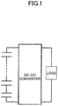
- a technique is conceivable which is designed to perform voltage conversion using a DC-DC converter as illustrated in FIG. 1 .
- problems such as a significant increase in loss, and an increase in circuit size, will occur.
- the problems also occur during charging to the capacitor.
- a charger is a sort of DC-DC converter, thus, charging is performed in a wide voltage range, loss in the charger will increase, and the size of the charger will become larger.
- a capacitor has an energy density which is significantly less than those of conventional secondary batteries, it is desirable to establish a voltage conversion scheme with higher efficiency as compared to a conventional DC-DC converter.
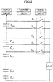
- a capacitor-based power supply apparatus which comprises a capacitor module composed of a plurality of capacitors connected in series, and a plurality of taps, as illustrated in FIG. 2 , wherein the apparatus is configured to change the number of ones of the series-connected capacitors which are to be connected to a load (to change the taps), to thereby reduce a fluctuation range of an output voltage thereof (the following Patent Document 1).
- Non-Patent Document 1 K. Z. Guo, et al.,: “Comparison and evaluation of charge equalization technique for series connected batteries” in Proc. IEEE PESC'06, pp. 1-6 (2006 )
- Patent document US5656915 discloses a battery charger comprising several taps connected to a charger and a balancing circuit.
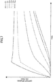
- FIG. 3 illustrates an output voltage (upper graph) and capacitor voltage curves (lower graph) obtained when the capacitor module is discharged using the above apparatus.
- FIG. 3 illustrates an output voltage (upper graph) and capacitor voltage curves (lower graph) obtained when the capacitor module is discharged using the above apparatus.
- a period of time for which a capacitor is to be connected to the load is also changed, so that a variation in charged/discharged state occurs between the capacitors, which causes a problem that energy of a part (in FIG. 2 , C y1 to C ym ) of the capacitors cannot be effectively utilized.
- the above problem can be solved by employing a technique of setting different capacitance values for each of a plurality of capacitors so as to allow voltages across the respective capacitors to become equal to each other at the end of the discharging. In this case, however, it is necessary to prepare a plurality of types of capacitors having different capacitance values.
- an electric energy storage system which comprises an electric energy storage module having a plurality of electric energy storage units connected in series, each of the plurality of electric energy storage units having one electric energy storage bank or a plurality of electric energy storage banks connected in series, and a balancing circuit connected to the electric energy storage module, it is an object of the present invention to provide a technique of equally utilizing the electric energy storage banks during charging/discharging. It is an object of the present invention to keep fluctuation of an input voltage from a charger or an output voltage to a load, within an arbitrary range, while equally utilizing the electric energy storage banks during charging/discharging.
- an electric energy storage system which comprises: an electric energy storage module having a plurality of electric energy storage units connected in series, each of the plurality of electric energy storage units having one electric energy storage bank or a plurality of electric energy storage banks connected in series; a charger for charging at least one of the electric energy storage banks; a balancing circuit connected to the electric energy storage module to correct a variation in charged/discharged state between the electric energy storage banks; a voltage detection section for detecting a voltage across or across each of one or more of the electric energy storage banks, or a voltage across the charger; a plurality of taps led out, respectively, from one of opposite terminals of the electric energy storage module and/or one or more of a plurality of series-connection points between the electric energy storage units, through respective switches; and a switch control section for switching the switches such that one of the plurality of taps is connected to one of opposite terminals of the charger, wherein the switch control section is operable, during a charging period, to sequentially
- an electric energy storage system which comprises: an electric energy storage module having a plurality of electric energy storage units connected in series, each of the plurality of electric energy storage units having one electric energy storage bank or a plurality of electric energy storage banks connected in series; a charger for charging at least one of the electric energy storage banks; a balancing circuit connected to the electric energy storage module to correct a variation in charged/discharged state between the electric energy storage banks; a voltage detection section for detecting a voltage across or across each of one or more of the electric energy storage banks, or a voltage across the charger; a plurality of taps led out, respectively, from one of opposite terminals of the electric energy storage module and/or the other terminal of the electric energy storage module and/or one or more of a plurality of series-connection points between the electric energy storage units, through respective switches; and a switch control section for switching the switches such that one of the plurality of taps is connected to one of opposite terminals of the charger or the other terminal of the charger,
- the switch control section is operable, after switching the switches predetermined times, with respect to each of a plurality of groups set by grouping the plurality of electric energy storage units, to subsequently sequentially switch the switches according to progress of the charging, based on a detection result from the voltage detection section and in a time division manner, so as to control the number of at least one of the plurality of electric energy storage units which is to be charged not via the balancing circuit but directly from the charger.
- the switch control section is operable, with respect to each of a plurality of groups set by grouping the plurality of electric energy storage units, to sequentially switch the switches according to progress of the charging, based on a detection result from the voltage detection section and in a time division manner, so as to control the number of at least one of the plurality of electric energy storage units which is to be charged not via the balancing circuit but directly from the charger.
- the switch control section is further operable to perform one or more times, after switching the switches predetermined times, with respect to each of groups set by re-grouping the plurality of electric energy storage units such that the number of the group set by the re-grouping is greater than the number of the group after switching the switches predetermined times, at least one subsequent sequential switching of the switch according to progress of the charging, based on a detection result from the voltage detection section and in a time division manner, so as to control the number of at least one of the plurality of electric energy storage units which is to be charged not via the balancing circuit but directly from the charger.
- an electric energy storage system which comprises: an electric energy storage module having a plurality of electric energy storage units connected in series, each of the plurality of electric energy storage units having one electric energy storage bank or a plurality of electric energy storage banks connected in series; a load to which electric energy is to be supplied from at least one of the electric energy storage banks; a balancing circuit connected to the electric energy storage module to correct a variation in charged/discharged state between the electric energy storage banks; a voltage detection section for detecting a voltage across or across each of one or more of the electric energy storage banks, or a discharging voltage from the electric energy storage banks to the load; a plurality of taps led out, respectively, from one of opposite terminals of the electric energy storage module and/or one or more of a plurality of series-connection points between the electric energy storage units, through respective switches; and a switch control section for switching the switches such that one of the plurality of taps is connected to one of opposite terminals of the load, wherein the
- an electric energy storage system which comprises: an electric energy storage module having a plurality of electric energy storage units connected in series, each of the plurality of electric energy storage units having one electric energy storage bank or a plurality of electric energy storage banks connected in series; a load to which electric energy is to be supplied from at least one of the electric energy storage banks; a balancing circuit connected to the electric energy storage module to correct a variation in charged/discharged state between the electric energy storage banks; a voltage detection section for detecting a voltage across or across each of one or more of the electric energy storage banks, or a discharging voltage from the electric energy storage banks to the load; a plurality of taps led out, respectively, from one of opposite terminals of the electric energy storage module and/or the other terminal of the electric energy storage module and/or one or more of a plurality of series-connection points between the electric energy storage units, through respective switches; and a switch control section for switching the switches such that one of the plurality of taps is connected to
- the switch control section is operable, with respect to each of a plurality of groups set by grouping the plurality of electric energy storage units, to sequentially switch the switches according to the discharged state, based on a detection result from the voltage detection section and in a time division manner, so as to control the number of at least one of the plurality of electric energy storage units which is to be discharged from at least one of the electric energy storage units not via the balancing circuit but directly to the load.
- the switch control section is further operable to perform one or more times, after switching the switches predetermined times, with respect to each of at least one group set by re-grouping the plurality of electric energy storage units such that the number of the at least one group set by the re-grouping is less than the number of the groups after switching the switches predetermined times, at least one subsequent sequential switching of the switches according to the discharged state, based on a detection result from the voltage detection section and in a time division manner, so as to control the number of at least one of the plurality of electric energy storage units which is to be discharged from at least one of the electric energy storage units not via the balancing circuit but directly to the load.
- an electric energy storage system which comprises: an electric energy storage module having a plurality of electric energy storage units connected in series, each of the plurality of electric energy storage units having one electric energy storage bank or a plurality of electric energy storage banks connected in series; a charger for charging at least one of the electric energy storage banks; a balancing circuit connected to the electric energy storage module to correct a variation in charged/discharged state between the electric energy storage banks; a voltage detection section for detecting a voltage across or across each of one or more of the electric energy storage banks, or a voltage across the charger; a plurality of taps led out, respectively, from one of opposite terminals of the electric energy storage module and/or one or more of a plurality of series-connection points between the electric energy storage units, through respective switches; and a switch control section for switching the switches such that one of the plurality of taps is connected to one of opposite terminals of the charger, wherein the switch control section is operable, during a charging period, to switch the
- an electric energy storage system which comprises: an electric energy storage module having a plurality of electric energy storage units connected in series, each of the plurality of electric energy storage units having one electric energy storage bank or a plurality of electric energy storage banks connected in series; a charger for charging at least one of the electric energy storage banks; a balancing circuit connected to the electric energy storage module to correct a variation in charged/discharged state between the electric energy storage banks; a voltage detection section for detecting a voltage across or across each of one or more of the electric energy storage banks, or a voltage across the charger; a plurality of taps led out, respectively, from one of opposite terminals of the electric energy storage module and/or the other terminal of the electric energy storage module and/or one or more of a plurality of series-connection points between the electric energy storage units, through respective switches; and a switch control section for switching the switches such that one of the plurality of taps is connected to one of opposite terminals of the charger or the other terminal of the charger,
- the switch control section is operable, after switching the switches predetermined times, with respect to each of a plurality of groups set by grouping the plurality of electric energy storage units, to sequentially switch the switches at least once, based on a detection result from the voltage detection section and in a time division manner, so as to reduce the number of at least one of the plurality of electric energy storage units which is to be charged not via the balancing circuit but directly from the charger.
- the switch control section is operable, with respect to each of a plurality of groups set by grouping the plurality of electric energy storage units, to switch the switches at least once, based on a detection result from the voltage detection section and in a time division manner, so as to reduce the number of at least one of the plurality of electric energy storage units which is to be charged not via the balancing circuit but directly from the charger.
- the switch control section is further operable to perform one or more times, after switching the switches predetermined times, with respect to each of groups set by re-grouping the plurality of electric energy storage units such that the number of the group set by the re-grouping is greater than the number of the group after switching the switches predetermined times, subsequent switching of the switches at least one time, based on a detection result from the voltage detection section and in a time division manner, so as to reduce the number of at least one of the plurality of electric energy storage units which is to be charged not via the balancing circuit but directly from the charger.
- an electric energy storage system which comprises: an electric energy storage module having a plurality of electric energy storage units connected in series, each of the plurality of electric energy storage units having one electric energy storage bank or a plurality of electric energy storage banks connected in series; a load to which electric energy is to be supplied from at least one of the electric energy storage banks; a balancing circuit connected to the electric energy storage module to correct a variation in charged/discharged state between the electric energy storage banks; a voltage detection section for detecting a voltage across or across each of one or more of the electric energy storage banks, or a discharging voltage from the electric energy storage banks to the load; a plurality of taps led out, respectively, from one of opposite terminals of the electric energy storage module and/or one or more of a plurality of series-connection points between the electric energy storage units, through respective switches; and a switch control section for switching the switches such that one of the plurality of taps is connected to one of opposite terminals of the load, wherein the
- an electric energy storage system which comprises: an electric energy storage module having a plurality of electric energy storage units connected in series, each of the plurality of electric energy storage units having one electric energy storage bank or a plurality of electric energy storage banks connected in series; a load to which electric energy is to be supplied from at least one of the electric energy storage banks; a balancing circuit connected to the electric energy storage module to correct a variation in charged/discharged state between the electric energy storage banks; a voltage detection section for detecting a voltage across or across each of one or more of the electric energy storage banks, or a discharging voltage from the electric energy storage banks to the load; a plurality of taps led out, respectively, from one of opposite terminals of the electric energy storage module and/or the other terminal of the electric energy storage module and/or one or more of a plurality of series-connection points between the electric energy storage units, through respective switches; and a switch control section for switching the switches such that one of the plurality of taps is connected to one
- the switch control section is operable, with respect to each of a plurality of groups set by grouping the plurality of electric energy storage units, to switch the switches at least once, based on a detection result from the voltage detection section and in a time division manner, so as to increase the number of at least one of the plurality of electric energy storage units which is to be discharged from at least one of the electric energy storage units not via the balancing circuit but directly to the load without involving the balancing circuit.
- the switch control section is further operable to perform one or more times, after switching the switches predetermined times, with respect to each of groups set by re-grouping the plurality of electric energy storage units such that the number of the group set by the re-grouping is greater than the number of the group after switching the switches predetermined times, subsequent switching of the switches at least one time, based on a detection result from the voltage detection section and in a time division manner, so as to increase the number of at least one of the plurality of electric energy storage units which is to be discharged from at least one of the electric energy storage units not via the balancing circuit but directly to the load.
- an electric energy storage system which comprises: an electric energy storage module having a plurality of electric energy storage units connected in series, each of the plurality of electric energy storage units having one electric energy storage bank or a plurality of electric energy storage banks connected in series; a charger for charging at least one of the electric energy storage banks; a balancing circuit connected to the electric energy storage module to correct a variation in charged/discharged state between the electric energy storage banks; a voltage detection section for detecting a voltage across or across each of one or more of the electric energy storage banks, or a voltage across the charger; a plurality of taps led out, respectively, from one of opposite terminals of the electric energy storage module and/or the other terminal of the electric energy storage module and/or one or more of a plurality of series-connection points between the electric energy storage units, through respective switches; and a switch control section for switching the switches such that one of the plurality of taps is connected to one of opposite terminals of the charger or the other terminal of the charger,
- an electric energy storage system which comprises: an electric energy storage module having a plurality of electric energy storage units connected in series, each of the plurality of electric energy storage units having one electric energy storage bank or a plurality of electric energy storage banks connected in series; a load to which electric energy is to be supplied from at least one of the electric energy storage banks; a balancing circuit connected to the electric energy storage module to correct a variation in charged/discharged state between the electric energy storage banks; a voltage detection section for detecting a voltage across or across each of one or more of the electric energy storage banks, or a discharging voltage from the electric energy storage banks to the load; a plurality of taps led out, respectively, from one of opposite terminals of the electric energy storage module and/or the other terminal of the electric energy storage module and/or one or more of a plurality of series-connection points between the electric energy storage units, through respective switches; and a switch control section for switching the switches such that one of the plurality of taps is
- the electric energy storage system of the present invention can efficiently perform voltage equalization between the electric energy storage banks, even in cases where the balancing circuit needs time to correct a variation in charged/discharged state by itself, due to influences of an internal resistance of each of the electric energy storage banks, characteristics of the balancing circuit, etc.
- the electric energy storage system of the present invention can keep a charging voltage from the charger or a discharging voltage to the load within an arbitrary range without using a DC-DC converter, etc., while equally maintaining voltages across the respective electric energy storage banks, by adequately selecting the taps connected to the charger or load, according to a voltage value of or of each of the electric energy storage banks or a voltage value in the charger.
- capacitor bank means a bank composed of a single capacitor cell or a plurality of capacitor cells connected in series, in parallel or in series-parallel.
- capacitor unit means a unit composed of a single capacitor bank, or a plurality of capacitor banks connected in series.
- capacitor module means a module composed of a plurality of capacitor units connected in series.
- electric energy storage cell means a capacitor, a secondary battery or the like.
- electric energy storage bank means a bank composed of a single electric energy storage cell or a plurality of electric energy storage cells connected in series, in parallel or in series-parallel.
- electric energy storage unit means a unit composed of a single electric energy storage bank, or a plurality of electric energy storage banks connected in series.
- electric energy storage module means a module composed of a plurality of electric energy storage units connected in series.
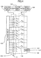
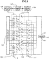
- FIG. 4 is a circuit diagram illustrating an electric energy storage system according to a first embodiment of the present invention.
- the balancing circuit is a circuit for correcting a variation in charged/discharged state between a plurality of electric energy storage banks making up an electric energy storage module, and is operable to perform energy transfer between the electric energy storage banks, i.e., a balancing operation, during both a charging period and a discharging period.
- the balancing circuit may be roughly classified into a type using a capacitor, a type using a coil and a type using a transformer.
- Various specific circuits of each of the three types are known (see, for example, the Patent Document 2 and the Non-Patent Document 1).
- switches S 2a to S 51a make up a switch group 110, and each of the switches S 2a to S 51a is connected between a corresponding one of the taps led out from respective ones of a plurality of series-connection points between the capacitor units, and a high-potential side terminal 101 of the charger 112.
- C 1 to C 100 indicate the respective capacitor banks.
- One of the switches S 2a to S 51a is turned on and directly connected to the high-potential side terminal 101 of the charger 112.
- a low-potential side terminal 102 of the charger is fixedly connected to the ground 0 of the capacitor module.
- a voltage detection circuit 106 is operable to detect a voltage across or acorss each of all or a part of the capacitor banks making up the capacitor module 109.
- a voltage determination circuit 107 is operable to compare the voltage detection result with a reference voltage, and then a switch control circuit 108 is operable, based on a result of the comparison, to switch the switches to control a charging voltage from the charger to fall within an arbitrary range, e.g., within an allowable voltage fluctuation range of the charger.
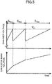
- FIG. 5 illustrates a charger voltage (upper graph) and a capacitor bank charging curve (lower graph) when a charging is performed in the system illustrated in FIG. 4 .
- the following description will be made on the assumption that an operation of the balancing circuit is ideal, i.e., voltages across the respective capacitor banks making up the capacitor module are evenly maintained by the balancing circuit under any conditions.
- the voltage across each of the capacitor banks will be gradually increased, and the charger voltage will reach Vin. Given that the voltages across the respective capacitor banks at this timing are equal to each other, the voltage across each of the capacitor banks is Vin/100.
- the switch control circuit 108 operates to turn off the switch S 51a and simultaneously turn on the switch S 50a , so that the tap for connecting the charger 112 and the capacitor module 109 is shifted toward the low potential side by one. This leads the charger voltage to be lowered by a value corresponding to a voltage across the capacitor banks C 100 and C 99 , i.e., (2 ⁇ Vin)/100.
- the switch control circuit 108 operates to turn off the switch S 50a and simultaneously turn on the switch S 49a , so that the tap for connecting the charger 112 and the capacitor module 109 is additionally shifted toward the low potential side by one. This leads the charger voltage to be lowered by a value corresponding to a voltage across the capacitor banks C 98 and C 97 , i.e., (2 ⁇ Vin)/98.
- ones of the capacitor units on the low potential side of the tap connected to the switch S 49a i.e., the capacitor banks C 1 to C 96 , are directly charged from the charger. Further, the capacitor banks C 97 to C 100 are charged by receiving electric charges from the capacitor banks C 1 to C 98 via the balancing circuit.
- the switches S 49a to S 2a are sequentially switched, according to the charger voltage so that the respective capacitor banks can be equally charged, while keeping the charger voltage within a certain arbitrary range.
- the above operation will be repeated until a total value of the rated voltages of the capacitor banks to be directly charged by the charger becomes less than the charging voltage by the charger.
- the above grouped charging will be repeated until the following relation is satisfied: x ⁇ Vc ⁇ Vin, where x is the number of series-connected ones of the capacitor banks which are to be directly charged by the charger. Based on repeating the above operation, it becomes possible to more equally perform the charging to each of the capacitor banks and thus shorten a charging time.
- FIG. 6 is a circuit diagram illustrating an electric energy storage system according to a second embodiment of the present invention.
- an element or component corresponding to that in FIG. 4 is defined by a common reference numeral or code, and duplicate description of the same element or component as that in the first embodiment will be omitted.
- the first embodiment is configured such that the high-potential side terminal 101 of the charger 112 is connected to the taps led out from the capacitor module 109, via the switch group 110.
- a switch group 111 composed of switches S 1b to S 50b is provided between the low-potential side terminal 102 of the charger 112 and the capacitor module 109.
- the switch control circuit 108 is operable, based on a voltage detection result from the voltage detection circuit 106, to sequentially switch the switches in order of S 1b , S 2b , -----, S 50b .
- FIG. 7 illustrates one example of charging waveforms of a part (C 1 , C 5 , C 10 , C 15 , C 20 and C 25 ) of the capacitor banks.
- FIG. 7 shows that the capacitor banks are not equally charged in the charging process.
- a part (C 6 to C 25 on a high potential side with respect to the switch S 5a ) of the capacitor banks which are not directly charged from a charger are charged by receiving electric charges from the directly charged capacitor banks (capacitor banks C 1 to C 5 on a low potential side with respect to the switch S 5a ) via the balancing circuit.
- the directly charged capacitor banks capacitor banks C 1 to C 5 on a low potential side with respect to the switch S 5a
- a voltage across each of the capacitor banks on the high potential side is apt to become less than that across each of the capacitor banks on the low potential side.
- progress of the charging becomes slower.
- FIG. 8 is a circuit diagram illustrating an electric energy storage system according to a third embodiment of the present invention.
- an element or component corresponding to that in FIG. 4 is defined by a common reference numeral or code, and duplicate description of the same element or component as that in the first embodiment will be omitted.
- the first embodiment is configured such that the low-potential side terminal 102 of the charger is directly connected to the ground 0 of the capacitor module 109.
- the low-potential side terminal 102 is fixedly connected to the series-connection point between the capacitor banks C 2 and C 3 , instead of being directly connected to the ground 0 of the capacitor module 109.
- the switch control circuit 108 is operable, based on a voltage detection result from the voltage detection circuit 106, to sequentially switch switches in order of S 51a , S 50a , -----, S 3a .
- the switch S 2a is turned on, so that the two capacitor banks C 1 and C 2 are directly charged, and the remaining capacitor banks are charged via the balancing circuit.
- the capacitor bank C 100 is located electrically farthest from the charger 112 (by a distance corresponding to ninety-eight capacitor banks), so that, when characteristics of the balancing circuit are not ideal, the capacitor bank C 100 exhibits the lowest voltage in the charging process.
- an electrical distance between the charger and the capacitor bank in the last phase of the charging can be shortened as compared to the system according to the first embodiment.
- the low-potential side terminal 102 of the charger is fixedly connected to the series-connection point between the capacitor banks C 2 and C 3 , so that the capacitor banks C 1 and C 2 cannot be directly charged by the charger 112. However, the capacitor banks C 1 and C 2 are charged by receiving electric charges from the remaining capacitor banks via the balancing circuit 105.
- the switch S 3a is turned on, so that the capacitor banks C 3 and C 4 are directly charged, and the remaining capacitor banks are charged via the balancing circuit.
- the capacitor bank C 100 located electrically farthest from the charger 112 is away from the charger by a distance corresponding to ninety-eight capacitor banks, whereas, in the system according to the third embodiment, the low-potential side terminal 102 of the charger 112 is connected to a position (the series-connection point between the capacitor banks C 2 and C 3 ) of higher potential side by a distance corresponding to two capacitor banks.
- the capacitor bank C 100 is away from the charger by a distance corresponding to ninety-six capacitor banks, i.e., closer to the charger by a distance corresponding to two capacitor banks, as compared to the system illustrated in FIG. 4 according to the first embodiment. This makes it possible to suppress a voltage variation between the capacitor banks in the last phase of the charging process at a lower level, as compared to the system illustrated in FIG. 4 according to the first embodiment.
- the high-potential side terminal 101 and the low-potential side terminal 102 of the charger 112 may be connected, respectively, to the switches S 27a and S 26a , or the switches S 26a and S 25a .
- a layout such as a position and the number of the switches, in the third embodiment, may be appropriately changed or modified, as needed.
- FIG. 9 is a circuit diagram illustrating an electric energy storage system according to a fourth embodiment of the present invention.
- an element or component corresponding to that in FIG. 4 is defined by a common reference numeral or code, and duplicate description of the same element or component as that in the first embodiment will be omitted.
- the high-potential side terminal 101 and the low-potential side terminal 102 of the charger 112 may be connected, respectively, to the switches S 27a and S 26a , or the switches S 26a and S 25a .
- some of the capacitor banks located on the low potential side, such as the capacitor bank C 1 ) are located electrically far from the charger.
- the fourth embodiment is directed, but not limited, to solving this problem.
- Switches S 2a to S 51a make up a first switch group 110', and switches S 1b to S 50b make up a second switch group 111'.
- Each of the switches S 2a to S 51a and each of the switches S 1b to S 50b are connected, respectively, between a corresponding one of the taps led out from respective ones of a plurality of series-connection points between the capacitor units, and a high-potential side terminal 101 of the charger 112, and between a corresponding one of the taps, and a low-potential side terminal 102 of the charger 112.
- a switch control circuit 108 operates to perform charging by turning on the switches S 51a and S 1b . At this time, all of the capacitor banks of the capacitor module 108 are directly charged from the charger 112.
- a voltage across each of the capacitor banks will be gradually increased, and a charger voltage will reach Vin.
- the switch control circuit 108 operates to turn off the switch S 51a and simultaneously turn on the switch S 50a , so that the tap for connecting the high-potential side terminal 101 of the charger 112 and the capacitor module 109 is shifted toward the low potential side by one.
- the capacitor banks C 1 to C 98 are charged not via the balancing circuit but directly by the charger, and the capacitor banks C 99 and C 100 are charged via the balancing circuit.
- the switch control circuit 108 operates to turn off the switch S 1b and simultaneously turn on the switch S 2b , so that the tap for connecting the low-potential side terminal 102 of the charger 112 and the capacitor module 109 is shifted toward the high potential side by one.
- the capacitor banks C 3 to C 98 are charged not via the balancing circuit but directly by the charger, and the capacitor banks C 1 , C 2 , C 99 and C 100 are charged via the balancing circuit.
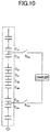
- FIG. 10 illustrates a state in which the switches are switched sequentially such that the capacitor banks C 50 and C 51 are located at the center of the capacitor banks which are directly charged by the charger, and the switches S 39a and S 13b are selected so that the total fifty-two capacitor banks C 25 to C 76 are directly charged by the charger (for simplifying illustration, the balancing circuit and the switches in a non-activated state are omitted).
- the remaining capacitor banks C 1 to C 24 and C 77 to C 100 are charged via the balancing circuit. Based on switching the switches in the above manner, it becomes possible to shorten an electrical distance between the charger and each of the capacitor banks to be charged via the balancing circuit, as much as possible.
- the capacitor banks of the capacitor module 109 are grouped into two groups, in such a manner that each of the capacitor banks around C m ⁇ 1/4 (i.e., C 25 ) and C m ⁇ 3/4 (i.e., C 75 ) is located at a center of each of the two groups of the series-connected capacitor banks to be directly charged by the charger, and the switch control circuit 108 operates to, with respect to each of the two groups, select two of the switches to perform charging by the charger in a time division manner.
- FIG. 11 illustrates a state in which the switch control circuit 108 operates to select the switches S 47a and S 29b and the switches S 22a and S 4b such that the capacitor banks around C 25 and C 75 are located at a center of each of the two groups of the series-connected capacitor banks to be directly charged by the charger, so that the group of capacitor banks C 57 to C 92 and the group of capacitor banks C 7 to C 42 are charged alternately and directly by the charger in a time division manner.
- the switch control circuit 108 operates to perform the charging via the switches S 47a and S 29b .
- the capacitor banks C 57 to C 92 are directly charged by the charger, and the remaining capacitor banks are charged via the balancing circuit.
- the switch control circuit 108 operates to perform the charging via the switches S 22a and S 4b
- the capacitor banks C 7 to C 42 are directly charged by the charger, and the remaining capacitor banks are charged via the balancing circuit.
- the capacitor banks of the capacitor module 109 are grouped into three groups, in such a manner that each of the capacitor banks around C m ⁇ 1/6 (i.e., C 17 ), C m ⁇ 3/6 (i.e., C 50 ) and C m ⁇ 5/6 (i.e., C 83 ) is located at a center of each of the three groups of the series-connected capacitor banks to be directly charged by the charger, and the switch control circuit 108 operates to, with respect to each of the three groups, select two of the switches to perform charging by the charger in a time division manner.
- C m ⁇ 1/6 i.e., C 17
- C m ⁇ 3/6 i.e., C 50
- C m ⁇ 5/6 i.e., C 83
- FIG. 12 illustrates a state in which the switch control circuit 108 operates to select the switches S 51a and S 35b , the switches S 34a and S 18b , the switches S 17a and S 1b , so that the group of capacitor banks C 69 to C 100 , the group of capacitor banks C 35 to C 66 , and the group of capacitor banks C 1 to C 32 are charged alternately and directly by the charger.
- the capacitor banks of the capacitor module 109 are grouped into four groups, in such a manner that each of the capacitor banks around C m ⁇ 1/8 (i.e., C 13 ), C m ⁇ 3/8 (i.e., C 38 ), C m ⁇ 5/8 (i.e., C 63 ) and C m ⁇ 7/8 (i.e., C 88 ) is located at a center of the series-connected capacitor banks to be directly charged by the charger, and the switch control circuit 108 operates to, with respect to each of the four groups, select switches to perform charging by the charger in a time division manner.
- FIG. 13 illustrates a state in which the switch control circuit 108 operates to select the switches S 48a and S 42b , the switches S 35a and S 29b , the switches S 23a and S 17b , the switches S 10a and S 4b , so that the group of capacitor banks C 83 to C 94 , the group of capacitor banks C 57 to C 68 , the group of capacitor banks C 33 to C 44 , and the group of capacitor banks C 7 to C 18 are charged alternately and directly by the charger.
- the above operation will be repeated until a total value of the rated voltages of the capacitor banks to be directly charged by the charger becomes less than the charging voltage Vin by the charger.
- the above grouped charging will be repeated until the following relation is satisfied: x ⁇ Vc ⁇ Vin, where x is the number of series-connected ones of the capacitor banks which are to be directly charged by the charger. Based on repeating the above operation, it becomes possible to more equally perform the charging to each of the capacitor banks and thus shorten a charging time.
- FIG. 14A illustrates one example of charging waveforms of a part (C 1 , C 5 , C 10 , C 15 , C 20 and C 25 ) of the capacitor banks.
- the charging waveforms of the respective capacitor banks well coincide with each other, which shows that the respective capacitor banks are equally charged.
- FIG. 14A also shows that the charging time for each of the capacitor banks is short. It is proven that significant improvement is achieved as compared to FIG. 7 illustrating the example of the first embodiment.
- the charging is started under a condition that a plurality of electric energy storage banks making up an electric energy storage module are not grouped.
- the charging may be started under a condition that the plurality of electric energy storage banks making up the electric energy storage module are grouped into a plurality of groups.
- the switches are switched such that the number of ones of the capacitor units which are to be directly charged by the charger is reduced.
- the switches may be switched such that, with respect to each of the plurality of groups, the same at least one capacitor unit is repeatedly subjected to direct charging by the charger, in a time division manner. This also makes it possible to shorten an electrical distance from the charger to the capacitor units to be charged via the balancing unit to more equally perform the charging to each of the capacitor banks.
- FIG. 14B illustrates one example of charging waveforms of a part (C 1 , C 5 , C 10 , C 15 , C 20 and C 25 ) of the capacitor banks.
- the charging waveforms of the respective capacitor banks excellently coincide with each other, which shows that the respective capacitor banks are equally charged. It is proven that significant improvement is achieved as compared to FIG. 7 illustrating the example of the first embodiment. Further, a comparison with FIG. 14A illustrating the aforementioned example shows that the capacitor banks can be more equally used, although it is necessary to take time for charging.
- a layout such as a position and the number of the switches, may be appropriately changed or modified, as long as the system of the layout may sequentially switch the switches such that one of the plurality of taps is connected to the one terminal or the other terminal of the charger, and control the number of at least one of the plurality of electric energy storage units which is to be charged not via the balancing circuit but directly from the charger.
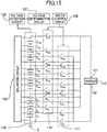
- a modified embodiment may include a system illustrated in FIG. 15 .
- the charger is a type in which an output voltage is likely to fluctuate, such as a solar cell
- switchings of the switches to reduce, retain or increase the number of ones of the electric energy storage units which are to be directly charged by the charger, according to a voltage detection result from the voltage detection circuit may be appropriately combined.
- a position of the electric energy storage unit where the charging is started, the number of groups in each grouping phase of the plurality of electric energy storage banks making up the electric energy storage module and the number of the electric energy storage banks in each of the groups, and the like may be arbitrarily selected.
- a timing of switching the switches by the switch control circuit 108 corresponds to a time when it is determined that the charger voltage reaches Vin, based on a voltage detection result from the voltage detection circuit 106.
- a criterial value of the charge voltage for the determination may be any voltage value which is less than Vin.
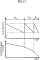
- FIG. 16 is a circuit diagram illustrating an electric energy storage system according to a fifth embodiment of the present invention.
- an element or component corresponding to that in FIG. 4 is defined by a common reference numeral or code, and duplicate description of the same element or component as that in the first embodiment will be omitted.
- the system according to the fifth embodiment is formed by replacing the charger in the system according to the first embodiment with a load 113, and fundamentally, performing operations (sequence of switching the switches , etc.) reverse to those during the charging enables the capacitor banks to be equally discharged while suppressing fluctuation of an output voltage.
- FIG. 17 illustrates operational waveforms when discharging is performed in the system illustrated in FIG. 16 .
- the discharging operation is started under a condition that the switch S 2a is turned on, and the switch control circuit 108 is operable to sequentially switch the switches toward a higher potential side to prevent a load voltage from becoming less than a certain arbitrary value (e.g., an allowable lower limit V low of the load voltage), by determining by the voltage determination circuit 107 the load voltage detected by the voltage detection circuit 106, so as to keep the load voltage within an arbitrary range.
- the capacitor bank (C 1 and C 2 during turn-on of the switch S 2a ) directly connected to the load is directly discharged to the load, and the remaining capacitor banks are discharged via the balancing circuit.
- FIG. 18 is a circuit diagram illustrating an electric energy storage system according to a sixth embodiment of the present invention.
- an element or component corresponding to that in FIG. 16 is defined by a common reference numeral or code, and duplicate description of the same element or component as that in the fifth embodiment will be omitted.
- the fifth embodiment is configured such that the switch group 110 is provided between a high-potential side terminal 121 of the load 113 and the capacitor module 109.
- a switch group 111 is provided between a low-potential side terminal 122 of the load 113 and the capacitor module 109.
- the switch control circuit 108 is operable, based on a voltage detection result from the voltage detection circuit 106, to switch switches in order of S 50b , S 49b , -----, S 1b .
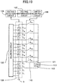
- FIG. 19 is a circuit diagram illustrating an electric energy storage system according to a seventh embodiment of the present invention.
- an element or component corresponding to that in FIG. 16 is defined by a common reference numeral or code, and duplicate description of the same element or component as that in the fifth embodiment will be omitted.
- the fifth embodiment is configured such that the low-potential side terminal 122 of the load 113 is directly connected to the ground 0 of the capacitor module 109.
- the low-potential side terminal 122 is not directly connected to the ground 0 of the capacitor module 109 but fixedly connected to the series-connection point between the capacitor banks C 2 and C 3 .
- the switch control circuit 108 is operable, based on a voltage detection result from the voltage detection circuit 106, to sequentially switch switches in order of S 3a , S 4a , -----, S 51a .
- an electrical distance between the load and the capacitor bank in an initial phase of a charging process can be shortened as compared to the system according to the fifth embodiment.
- the switch S 3a is turned on, so that the capacitor banks C 3 and C 4 are directly discharged to the load, and the capacitor banks C 1 , C 2 and C 5 to C 100 are discharged via the balancing circuit.
- the capacitor bank C 100 located electrically farthest from the load 113 is away from the load by a distance corresponding to ninety-eight capacitor banks, whereas, in the system according to the seventh embodiment, the low-potential side terminal 122 of the load 113 is connected to a position (the series-connection point between the capacitor banks C 2 and C 3 ) of higher potential side by a distance corresponding to two capacitor banks.
- the capacitor bank C 100 is away from the load by a distance corresponding to ninety-six capacitor banks, i.e., closer to the load by a distance corresponding to two capacitor banks, as compared to the system according to the fifth embodiment. This makes it possible to suppress a voltage variation between the capacitor banks in the initial phase of the charging process at a lower level, as compared to the system according to the fifth embodiment.
- the high-potential side terminal 121 and the low-potential side terminal 122 of the load 113 may be connected, respectively, to the switches S 27a and S 26a , or the switches S 26a and S 25a .
- a layout such as a position and the number of the switches, in the fifth to seventh embodiments, may be appropriately changed or modified, as needed.
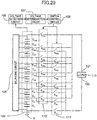
- FIG. 20 is a circuit diagram illustrating an electric energy storage system according to an eighth embodiment of the present invention.
- an element or component corresponding to that in FIG. 16 is defined by a common reference numeral or code, and duplicate description of the same element or component as that in the fifth embodiment will be omitted.
- the system according to the eighth embodiment is formed by replacing the charger in the system according to the fourth embodiment with a load 113, and fundamentally, performing operations (sequence of switching the switches , sequence of grouping of the capacitor banks, etc.) reverse to those during the charging enables the capacitor banks to be equally discharged while suppressing fluctuation of an output voltage.
- Switches S 2a to S 51a make up a first switch group 110', and switches S 1b to S 50b make up a second switch group 111'.
- Each of the switches S 2a to S 51a and each of the switches S 1b to S 50b are connected, respectively, between a corresponding one of the taps led out from respective ones of a plurality of series-connection points between the capacitor units, and a high-potential side terminal 121 of the load 113, and between a corresponding one of the taps, and a low-potential side terminal 122 of the load 113.
- the eighth embodiment is fundamentally designed to perform operations reverse to those in the fourth embodiment designed for a charging process. Then, the following description will be made based on an example where the discharging process is started under a condition that the number of groups is four, i.e. under a condition that the plurality of capacitor banks making up the capacitor module are grouped into four groups.
- the capacitor banks in the capacitor module 109 are grouped into four groups, in such a manner that each of the capacitor banks around C m ⁇ 1/8 (i.e., C 13 ), C m ⁇ 3/8 (i.e., C 38 ), C m ⁇ 5/8 (i.e., C 63 ) and C m ⁇ 7/8 (i.e., C 88 ) is located at a center of each of the four groups of the series-connected capacitor banks to be directly discharged to the load, and the switch control circuit 108 operates to, with respect to each of the four groups, select the switches in such a manner that each of the banks (around banks C 13 , C 38 , C 63 and C 88 ) around at respective centers of the series-connected capacitor banks making up each of the groups is located at a center of each of the groups of the series-connected capacitor banks to be directly discharged to the load, to perform discharging to the load in a time division manner.
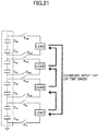
- FIG. 21 illustrates a state in which the switch control circuit 108 operates to select the switches S 8a and S 7b , the switches S 20a and S 19b , the switches S 33a and S 32b , the switches S 45a and S 44b , so that the group of capacitor banks C 13 to C 14 , the group of capacitor banks C 37 to C 38 , the group of capacitor banks C 63 to C 64 , and the group of capacitor banks C 87 to C 88 are discharged alternately to the load.
- a discharge operation of the four groups will be described by taking the group including the capacitor bank C 13 as an example. The discharge operation is started under a condition that the switches S 8a and S 7b are turned on.
- the switch control circuit 108 operates to turn off the switch S 8a and simultaneously turn on the switch S 9a , so that the tap for connecting the high-potential side terminal 121 of the load 113 and the capacitor module 109 is shifted toward higher potential side by one.
- the capacitor banks C 13 to C 16 are discharged not via the balancing circuit but directly to the load, and the remaining capacitor banks are discharged via the balancing circuit.
- the switch control circuit 108 operates to turn off the switch S 7b and simultaneously turn on the switch S 6b , so that the tap for connecting the low-potential side terminal 122 of the load 113 and the capacitor module 109 is shifted toward lower potential side by one.
- the capacitor banks C 11 to C 16 are discharged not via the balancing circuit but directly to the load, and the remaining capacitor banks are discharged via the balancing circuit. Based on switching the switches in this manner, it becomes possible to equalize times for allowing the respective capacitor banks to be directly discharged to the load, as evenly as possible, which is desirable in view of keeping voltages of the respective capacitor banks as equal as possible.
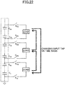
- the capacitor banks of the capacitor module 109 are grouped into three groups, in such a manner that each of the capacitor banks around C m ⁇ 1/6 (i.e., C 17 ), C m ⁇ 3/6 (i.e., C 50 ) and C m ⁇ 5/6 (i.e., C 83 ) is located at a center of each of the three groups of the series-connected capacitor banks to be directly discharged to the load, and the switch control circuit 108 operates to, with respect to each of the three groups, select the switches in such a manner that each of the capacitor banks (capacitor banks around C 17 , C 50 and C 83 ) around at respective centers of the three groups of series-connected capacitor banks is located at
- FIG. 22 illustrates a state in which the switch control circuit 108 operates to select the switches S 15a and S 3b , the switches S 32a and S 20b , and the switches S 49 and S 37b , so that the group of capacitor banks C 5 to C 28 , the group of capacitor banks C 39 to C 62 and the group of capacitor banks C 73 to C 96 are discharged alternately to the load.
- the switches are switched by the switch control circuit 108 in each of the groups in the same manner as above, and its description will be omitted.
- FIG. 23 illustrates a state in which the switches S 39a and S 13b are selected, so that the capacitor banks C 25 to C 76 are directly discharged to the load, and the remaining capacitor banks are discharged via the balancing circuit.
- the switches are switched to increase the number of ones of the capacitor units which are to be directly discharged to the load.
- the switches may be switched such that, with respect to each of the plurality of groups, the same at least one capacitor unit is repeatedly subjected to direct discharging to the load, in a time division manner. This also makes it possible to shorten an electrical distance from the load to the capacitor units to be discharged via the balancing unit to more equally perform the discharging from each of the capacitor banks.
- a layout such as a position and the number of the switches, may be arbitrarily changed or modified, as long as the system of the layout may sequentially switch the switches such that one of the plurality of taps is connected to the one terminal or the other terminal of the load, and control the number of at least one of the plurality of electric energy storage units which is to be discharged not via the balancing circuit but directly to the load, as with the fourth embodiment.
- the switches may be switched to reduce the number of ones of the electric energy storage units which are to be directly discharged to the load during the discharging process.
- a position of the electric energy storage unit where the discharging is started, the number of groups in each grouping phase of the plurality of electric energy storage banks making up the electric energy storage module and the number of the electric energy storage banks in each of the groups, and the like may be arbitrarily selected.
- a timing of switching the switch by the switch control circuit 108 corresponds to a time when it is determined that the load voltage reaches V low , based on a voltage detection result from the voltage detection circuit 106.
- a criterial value of the load voltage for the determination may be any voltage value which is greater than V low and equal to or less than an allowable upper voltage limit of the load.
- the voltage detection circuit 106 is compared with a reference voltage in the voltage determination circuit 107, and the switches are switched by the switch control circuit 108 based on a result of the comparison to control a charging voltage from a charger or a discharging voltage to a load to fall within a certain arbitrary range.
- the charging voltage from the charger or the discharging voltage to the load may be detected to switch the switches based on a result of the detection.
- the capacitor bank voltage, the charging voltage from the charger, and the discharging voltage to the load exhibit the same tendency as the characteristics described above.
- the number of capacitor banks making up the capacitor unit may be arbitrarily changed depending on positions, for example, in such a manner that the number is set to h at one position and to (h + 1) at another position.
- the rated voltage of each of the capacitor banks is Vc.
- the rated voltage may be arbitrarily changed in each of the capacitor banks, for example, in such a manner that one of the capacitor banks has Vc', and one of the capacitor banks has Vc".
- the present invention may be applied to a system using any electric energy storage bank other than the capacitor bank, such as a secondary battery.
Landscapes
- Engineering & Computer Science (AREA)
- Power Engineering (AREA)
- Manufacturing & Machinery (AREA)
- Chemical & Material Sciences (AREA)
- Chemical Kinetics & Catalysis (AREA)
- Electrochemistry (AREA)
- General Chemical & Material Sciences (AREA)
- Charge And Discharge Circuits For Batteries Or The Like (AREA)
- Secondary Cells (AREA)
Applications Claiming Priority (2)
| Application Number | Priority Date | Filing Date | Title |
|---|---|---|---|
| JP2009202684A JP5440918B2 (ja) | 2009-09-02 | 2009-09-02 | バランス回路を備えた蓄電装置 |
| PCT/JP2010/065041 WO2011027828A1 (ja) | 2009-09-02 | 2010-09-02 | バランス回路を備えた蓄電装置 |
Publications (3)
| Publication Number | Publication Date |
|---|---|
| EP2475067A1 EP2475067A1 (en) | 2012-07-11 |
| EP2475067A4 EP2475067A4 (en) | 2016-06-08 |
| EP2475067B1 true EP2475067B1 (en) | 2019-04-10 |
Family
ID=43649362
Family Applications (1)
| Application Number | Title | Priority Date | Filing Date |
|---|---|---|---|
| EP10813776.1A Active EP2475067B1 (en) | 2009-09-02 | 2010-09-02 | Electricity-storage device provided with balancing circuit |
Country Status (7)
| Country | Link |
|---|---|
| US (1) | US9318779B2 (enExample) |
| EP (1) | EP2475067B1 (enExample) |
| JP (1) | JP5440918B2 (enExample) |
| KR (1) | KR101726901B1 (enExample) |
| CN (1) | CN102577016B (enExample) |
| TW (1) | TWI499162B (enExample) |
| WO (1) | WO2011027828A1 (enExample) |
Families Citing this family (27)
| Publication number | Priority date | Publication date | Assignee | Title |
|---|---|---|---|---|
| JP4590520B1 (ja) | 2009-09-02 | 2010-12-01 | 日本蓄電器工業株式会社 | 交流出力可能な蓄電装置 |
| JP5440918B2 (ja) | 2009-09-02 | 2014-03-12 | 独立行政法人 宇宙航空研究開発機構 | バランス回路を備えた蓄電装置 |
| US9385553B2 (en) * | 2011-03-18 | 2016-07-05 | Asahi Kasei Microdevices Corporation | Balance charging circuit for series-connected storage cells and balance charging method for series-connected storage cells |
| DE102012209657A1 (de) * | 2012-06-08 | 2013-12-12 | Robert Bosch Gmbh | Verfahren und Vorrichtung zur Ermittlung des Innenwiderstandes von Batteriezellen einer Batterie |
| JP6034602B2 (ja) * | 2012-07-02 | 2016-11-30 | ローム株式会社 | 制御回路、キャパシタモジュール、電池モジュール、電源回路、それらを用いた家庭用蓄電池および車両 |
| JP6134520B2 (ja) * | 2013-01-25 | 2017-05-24 | Fdk株式会社 | バランス補正装置及び蓄電装置 |
| JP6196466B2 (ja) | 2013-05-10 | 2017-09-13 | Fdk株式会社 | 電源装置 |
| FR3019217B1 (fr) * | 2014-03-27 | 2018-07-27 | Safran Helicopter Engines | Procede et systeme de reactivation rapide de turbomachine |
| US20160105044A1 (en) * | 2014-10-08 | 2016-04-14 | Panasonic Intellectual Property Management Co., Ltd. | Power-storage-system control method and power-storage-system control apparatus |
| EP3026750A1 (de) * | 2014-11-28 | 2016-06-01 | Siemens Aktiengesellschaft | Verfahren zum Symmetrieren eines Energiespeichersystems |
| US9912164B2 (en) * | 2014-12-24 | 2018-03-06 | Intel Corporation | Multisource power delivery system |
| WO2016209698A1 (en) | 2015-06-26 | 2016-12-29 | Amber Kinetics, Inc. | Switching fabric for energy storage and power conversion |
| CN107294145A (zh) * | 2016-03-30 | 2017-10-24 | 通用电气公司 | 充电装置、系统和方法 |
| KR101837548B1 (ko) * | 2016-04-07 | 2018-04-26 | 삼화콘덴서공업 주식회사 | 커패시터 관리 시스템 |
| JP6883396B2 (ja) * | 2016-08-25 | 2021-06-09 | 矢崎総業株式会社 | 急速充電装置 |
| DE102016122444A1 (de) * | 2016-11-22 | 2018-05-24 | HELLA GmbH & Co. KGaA | Zweispannungsbatterie |
| EP3340412B1 (de) * | 2016-12-21 | 2019-03-06 | Airbus Defence and Space GmbH | Energieversorgungsschaltung, elektrisches antriebssystem und flugkörper mit einem elektrischen antriebssystem |
| US10822858B2 (en) | 2017-07-24 | 2020-11-03 | Gmi Holdings, Inc. | Power supply for movable barrier opener with brushless DC motor |
| JP6928347B2 (ja) * | 2017-08-02 | 2021-09-01 | NExT−e Solutions株式会社 | 管理装置、蓄電装置、蓄電システム、及び、電気機器 |
| CN107591818B (zh) * | 2017-08-11 | 2020-06-26 | 烟台海珐电气科技有限公司 | 一种解决低负载无功过补、欠补问题的无功补偿方法 |
| JP7009915B2 (ja) * | 2017-10-27 | 2022-01-26 | 株式会社デンソー | 蓄電システム |
| US10444295B2 (en) * | 2017-12-20 | 2019-10-15 | National Chung Shan Institute Of Science And Technology | Battery balance management circuit |
| JP7170173B2 (ja) * | 2018-03-28 | 2022-11-14 | パナソニックIpマネジメント株式会社 | 蓄電デバイス用の放電回路、蓄電システム及びそれを備える車両 |
| FR3085540B1 (fr) * | 2018-08-31 | 2020-09-25 | St Microelectronics Rousset | Dispositif integre de mesure temporelle a constante de temps ultra longue et procede de fabrication |
| JP7044671B2 (ja) * | 2018-09-07 | 2022-03-30 | Fdk株式会社 | 蓄電装置及び充電方法 |
| KR102932560B1 (ko) * | 2019-09-27 | 2026-03-03 | 보스톤 싸이엔티픽 싸이메드 인코포레이티드 | 레이저 펄싱을 제어하기 위한 시스템들 및 방법들 |
| KR102366121B1 (ko) * | 2020-04-02 | 2022-02-22 | 엘지전자 주식회사 | 전기자동차 충전장치 |
Family Cites Families (33)
| Publication number | Priority date | Publication date | Assignee | Title |
|---|---|---|---|---|
| US3100851A (en) | 1959-11-03 | 1963-08-13 | Ling Temco Vought Inc | High power synthetic waveform generator |
| FR2418977A1 (fr) | 1978-03-02 | 1979-09-28 | Labo Electronique Physique | Onduleur universel |
| JPH02123928A (ja) * | 1988-10-31 | 1990-05-11 | Mitsubishi Metal Corp | 電源装置 |
| CN1022529C (zh) | 1990-06-06 | 1993-10-20 | 北京理工大学 | 高频开关电容型逆变器 |
| JPH07115728A (ja) | 1992-08-28 | 1995-05-02 | Tai-Her Yang | 複数の独立直流電源による多段階複電圧出力回路 |
| GB2265502A (en) | 1993-03-22 | 1993-09-29 | Yang Tai Her | Dc-ac converter |
| JPH08182212A (ja) * | 1994-12-26 | 1996-07-12 | Nissan Motor Co Ltd | 組電池充電制御回路 |
| JPH08308249A (ja) | 1995-04-27 | 1996-11-22 | Matsushita Electric Works Ltd | 電源装置 |
| US5656915A (en) * | 1995-08-28 | 1997-08-12 | Eaves; Stephen S. | Multicell battery pack bilateral power distribution unit with individual cell monitoring and control |
| US5659237A (en) * | 1995-09-28 | 1997-08-19 | Wisconsin Alumni Research Foundation | Battery charging using a transformer with a single primary winding and plural secondary windings |
| US5710504A (en) * | 1996-05-20 | 1998-01-20 | The Board Of Trustees Of The University Of Illinois | Switched capacitor system for automatic battery equalization |
| JP3922655B2 (ja) * | 1996-07-12 | 2007-05-30 | 株式会社東京アールアンドデー | 電源装置の制御システムおよび電源装置の制御方法 |
| US6181106B1 (en) * | 1996-07-18 | 2001-01-30 | Curtis Instruments, Inc. | Sequential high-rate charging of battery cells |
| JP3594288B2 (ja) | 1999-01-18 | 2004-11-24 | 株式会社岡村研究所 | 直列接続段数切り換え式キャパシタ電源装置 |
| US6121751A (en) * | 1999-03-11 | 2000-09-19 | Lockheed Martin Corporation | Battery charger for charging a stack of multiple lithium ion battery cells |
| JP2002345157A (ja) | 2001-03-16 | 2002-11-29 | Kazumichi Fujioka | 充放電装置 |
| JP3858893B2 (ja) * | 2001-10-01 | 2006-12-20 | サンケン電気株式会社 | 電圧バランス回路、電圧検出用回路、電圧バランス方法及び電圧検出方法 |
| JP2003134686A (ja) * | 2001-10-23 | 2003-05-09 | Japan Storage Battery Co Ltd | 充電装置 |
| JP3867581B2 (ja) * | 2002-01-17 | 2007-01-10 | 松下電器産業株式会社 | 組電池システム |
| US7378818B2 (en) * | 2002-11-25 | 2008-05-27 | Tiax Llc | Bidirectional power converter for balancing state of charge among series connected electrical energy storage units |
| TW571452B (en) * | 2002-12-13 | 2004-01-11 | Quanta Comp Inc | Charging-type electrical potential balance device |
| JP4130186B2 (ja) | 2004-11-12 | 2008-08-06 | 三洋電機株式会社 | パック電池 |
| DE102005041824A1 (de) | 2005-09-02 | 2007-03-08 | Siemens Ag | Vorrichtung und Verfahren zum Ladungsausgleich zwischen den Einzelzellen eines Doppelschichtkondensators, insbesondere in einem Mehrspannungs-Kraftfahrzeugbordnetz |
| JP4368924B2 (ja) * | 2005-10-19 | 2009-11-18 | 有限会社ティーエム | キャパシタを用いた蓄電装置とその制御方法 |
| JP4157552B2 (ja) | 2005-12-09 | 2008-10-01 | 独立行政法人 宇宙航空研究開発機構 | 蓄電素子のための電圧バランス回路 |
| JP2007312517A (ja) | 2006-05-18 | 2007-11-29 | Nippon Yusoki Co Ltd | 電源装置 |
| DE102006028503A1 (de) * | 2006-06-21 | 2007-12-27 | Siemens Ag | Vorrichtung und Verfahren zum Laden eines Energiespeichers |
| TW200810317A (en) * | 2006-08-01 | 2008-02-16 | Aeneas Energy Technology Co Ltd | Charging circuit of serial-connected batteries without damaging in uniform charging |
| JP4352183B2 (ja) | 2007-02-28 | 2009-10-28 | 独立行政法人 宇宙航空研究開発機構 | 蓄電モジュール |
| TW201103229A (en) * | 2009-07-13 | 2011-01-16 | Sanyang Industry Co Ltd | Charging device with balance circuit |
| US9197081B2 (en) * | 2009-08-28 | 2015-11-24 | The Charles Stark Draper Laboratory, Inc. | High-efficiency battery equalization for charging and discharging |
| JP5440918B2 (ja) | 2009-09-02 | 2014-03-12 | 独立行政法人 宇宙航空研究開発機構 | バランス回路を備えた蓄電装置 |
| JP4590520B1 (ja) | 2009-09-02 | 2010-12-01 | 日本蓄電器工業株式会社 | 交流出力可能な蓄電装置 |
-
2009
- 2009-09-02 JP JP2009202684A patent/JP5440918B2/ja active Active
-
2010
- 2010-09-01 TW TW099129419A patent/TWI499162B/zh active
- 2010-09-02 KR KR1020127005537A patent/KR101726901B1/ko active Active
- 2010-09-02 CN CN201080039577.3A patent/CN102577016B/zh active Active
- 2010-09-02 WO PCT/JP2010/065041 patent/WO2011027828A1/ja not_active Ceased
- 2010-09-02 EP EP10813776.1A patent/EP2475067B1/en active Active
-
2012
- 2012-03-02 US US13/411,480 patent/US9318779B2/en active Active
Non-Patent Citations (1)
| Title |
|---|
| None * |
Also Published As
| Publication number | Publication date |
|---|---|
| JP2011055649A (ja) | 2011-03-17 |
| JP5440918B2 (ja) | 2014-03-12 |
| KR101726901B1 (ko) | 2017-04-26 |
| TW201125259A (en) | 2011-07-16 |
| TWI499162B (zh) | 2015-09-01 |
| EP2475067A1 (en) | 2012-07-11 |
| WO2011027828A1 (ja) | 2011-03-10 |
| EP2475067A4 (en) | 2016-06-08 |
| US20120194138A1 (en) | 2012-08-02 |
| KR20120090956A (ko) | 2012-08-17 |
| CN102577016A (zh) | 2012-07-11 |
| US9318779B2 (en) | 2016-04-19 |
| CN102577016B (zh) | 2014-08-27 |
Similar Documents
| Publication | Publication Date | Title |
|---|---|---|
| EP2475067B1 (en) | Electricity-storage device provided with balancing circuit | |
| KR101922370B1 (ko) | 전지 밸런싱 및 충전 장치 및 방법 | |
| KR102120797B1 (ko) | 배터리 충방전 장치 및 방법 | |
| US8773070B2 (en) | Apparatus and method for balancing charge capacity of battery cell | |
| CN103620860B (zh) | 用于提供中间电压的电池系统和方法 | |
| EP3128639B1 (en) | Electricity storage element charging method and electricity storage device | |
| US9356467B2 (en) | Charge balancing circuit for series connected chains of charge storage elements | |
| US9831689B2 (en) | Battery cell balancing method | |
| US10027135B2 (en) | Apparatus for balancing battery power | |
| WO2007145464A1 (en) | Charge equalization apparatus and method | |
| WO2012042401A2 (en) | Charge balancing system | |
| CN107134599A (zh) | 一种串联电池组的电压均衡电路及其工作方法 | |
| US20180226808A1 (en) | Battery module balancing method using single inductor | |
| KR101957841B1 (ko) | 태양광 전력 저장 배터리 밸런싱 장치 | |
| JP2016046836A (ja) | 非絶縁型セルバランス回路 | |
| WO2018223168A1 (en) | Energy transfer arrangement and method of controlling the same | |
| JP2025536659A (ja) | モジュールバランシング方法およびこれを適用したバッテリー管理システム | |
| CN114726024A (zh) | 并联电池模组的电容模块均衡电路 | |
| KR20150012670A (ko) | 임피던스매칭 직-병렬전환회로장치 |
Legal Events
| Date | Code | Title | Description |
|---|---|---|---|
| PUAI | Public reference made under article 153(3) epc to a published international application that has entered the european phase |
Free format text: ORIGINAL CODE: 0009012 |
|
| 17P | Request for examination filed |
Effective date: 20120319 |
|
| AK | Designated contracting states |
Kind code of ref document: A1 Designated state(s): AL AT BE BG CH CY CZ DE DK EE ES FI FR GB GR HR HU IE IS IT LI LT LU LV MC MK MT NL NO PL PT RO SE SI SK SM TR |
|
| DAX | Request for extension of the european patent (deleted) | ||
| RA4 | Supplementary search report drawn up and despatched (corrected) |
Effective date: 20160506 |
|
| RIC1 | Information provided on ipc code assigned before grant |
Ipc: H02J 7/02 20060101AFI20160429BHEP Ipc: H01M 10/44 20060101ALI20160429BHEP Ipc: H02J 7/00 20060101ALI20160429BHEP |
|
| STAA | Information on the status of an ep patent application or granted ep patent |
Free format text: STATUS: REQUEST FOR EXAMINATION WAS MADE |
|
| STAA | Information on the status of an ep patent application or granted ep patent |
Free format text: STATUS: EXAMINATION IS IN PROGRESS |
|
| 17Q | First examination report despatched |
Effective date: 20180322 |
|
| GRAP | Despatch of communication of intention to grant a patent |
Free format text: ORIGINAL CODE: EPIDOSNIGR1 |
|
| STAA | Information on the status of an ep patent application or granted ep patent |
Free format text: STATUS: GRANT OF PATENT IS INTENDED |
|
| INTG | Intention to grant announced |
Effective date: 20181023 |
|
| RIN1 | Information on inventor provided before grant (corrected) |
Inventor name: KUKITA AKIO Inventor name: UNO MASATOSHI Inventor name: SEKIDO TSUTOMU Inventor name: ITO KAZUSHIGE |
|
| GRAS | Grant fee paid |
Free format text: ORIGINAL CODE: EPIDOSNIGR3 |
|
| GRAA | (expected) grant |
Free format text: ORIGINAL CODE: 0009210 |
|
| STAA | Information on the status of an ep patent application or granted ep patent |
Free format text: STATUS: THE PATENT HAS BEEN GRANTED |
|
| AK | Designated contracting states |
Kind code of ref document: B1 Designated state(s): AL AT BE BG CH CY CZ DE DK EE ES FI FR GB GR HR HU IE IS IT LI LT LU LV MC MK MT NL NO PL PT RO SE SI SK SM TR |
|
| REG | Reference to a national code |
Ref country code: GB Ref legal event code: FG4D |
|
| REG | Reference to a national code |
Ref country code: CH Ref legal event code: EP Ref country code: AT Ref legal event code: REF Ref document number: 1119996 Country of ref document: AT Kind code of ref document: T Effective date: 20190415 |
|
| REG | Reference to a national code |
Ref country code: IE Ref legal event code: FG4D |
|
| REG | Reference to a national code |
Ref country code: DE Ref legal event code: R096 Ref document number: 602010058197 Country of ref document: DE |
|
| REG | Reference to a national code |
Ref country code: NL Ref legal event code: MP Effective date: 20190410 |
|
| REG | Reference to a national code |
Ref country code: LT Ref legal event code: MG4D |
|
| REG | Reference to a national code |
Ref country code: AT Ref legal event code: MK05 Ref document number: 1119996 Country of ref document: AT Kind code of ref document: T Effective date: 20190410 |
|
| PG25 | Lapsed in a contracting state [announced via postgrant information from national office to epo] |
Ref country code: NL Free format text: LAPSE BECAUSE OF FAILURE TO SUBMIT A TRANSLATION OF THE DESCRIPTION OR TO PAY THE FEE WITHIN THE PRESCRIBED TIME-LIMIT Effective date: 20190410 |
|
| PG25 | Lapsed in a contracting state [announced via postgrant information from national office to epo] |
Ref country code: FI Free format text: LAPSE BECAUSE OF FAILURE TO SUBMIT A TRANSLATION OF THE DESCRIPTION OR TO PAY THE FEE WITHIN THE PRESCRIBED TIME-LIMIT Effective date: 20190410 Ref country code: SE Free format text: LAPSE BECAUSE OF FAILURE TO SUBMIT A TRANSLATION OF THE DESCRIPTION OR TO PAY THE FEE WITHIN THE PRESCRIBED TIME-LIMIT Effective date: 20190410 Ref country code: AL Free format text: LAPSE BECAUSE OF FAILURE TO SUBMIT A TRANSLATION OF THE DESCRIPTION OR TO PAY THE FEE WITHIN THE PRESCRIBED TIME-LIMIT Effective date: 20190410 Ref country code: PT Free format text: LAPSE BECAUSE OF FAILURE TO SUBMIT A TRANSLATION OF THE DESCRIPTION OR TO PAY THE FEE WITHIN THE PRESCRIBED TIME-LIMIT Effective date: 20190910 Ref country code: NO Free format text: LAPSE BECAUSE OF FAILURE TO SUBMIT A TRANSLATION OF THE DESCRIPTION OR TO PAY THE FEE WITHIN THE PRESCRIBED TIME-LIMIT Effective date: 20190710 Ref country code: LT Free format text: LAPSE BECAUSE OF FAILURE TO SUBMIT A TRANSLATION OF THE DESCRIPTION OR TO PAY THE FEE WITHIN THE PRESCRIBED TIME-LIMIT Effective date: 20190410 Ref country code: HR Free format text: LAPSE BECAUSE OF FAILURE TO SUBMIT A TRANSLATION OF THE DESCRIPTION OR TO PAY THE FEE WITHIN THE PRESCRIBED TIME-LIMIT Effective date: 20190410 Ref country code: ES Free format text: LAPSE BECAUSE OF FAILURE TO SUBMIT A TRANSLATION OF THE DESCRIPTION OR TO PAY THE FEE WITHIN THE PRESCRIBED TIME-LIMIT Effective date: 20190410 |
|
| PG25 | Lapsed in a contracting state [announced via postgrant information from national office to epo] |
Ref country code: LV Free format text: LAPSE BECAUSE OF FAILURE TO SUBMIT A TRANSLATION OF THE DESCRIPTION OR TO PAY THE FEE WITHIN THE PRESCRIBED TIME-LIMIT Effective date: 20190410 Ref country code: BG Free format text: LAPSE BECAUSE OF FAILURE TO SUBMIT A TRANSLATION OF THE DESCRIPTION OR TO PAY THE FEE WITHIN THE PRESCRIBED TIME-LIMIT Effective date: 20190710 Ref country code: GR Free format text: LAPSE BECAUSE OF FAILURE TO SUBMIT A TRANSLATION OF THE DESCRIPTION OR TO PAY THE FEE WITHIN THE PRESCRIBED TIME-LIMIT Effective date: 20190711 Ref country code: PL Free format text: LAPSE BECAUSE OF FAILURE TO SUBMIT A TRANSLATION OF THE DESCRIPTION OR TO PAY THE FEE WITHIN THE PRESCRIBED TIME-LIMIT Effective date: 20190410 |
|
| PG25 | Lapsed in a contracting state [announced via postgrant information from national office to epo] |
Ref country code: IS Free format text: LAPSE BECAUSE OF FAILURE TO SUBMIT A TRANSLATION OF THE DESCRIPTION OR TO PAY THE FEE WITHIN THE PRESCRIBED TIME-LIMIT Effective date: 20190810 Ref country code: AT Free format text: LAPSE BECAUSE OF FAILURE TO SUBMIT A TRANSLATION OF THE DESCRIPTION OR TO PAY THE FEE WITHIN THE PRESCRIBED TIME-LIMIT Effective date: 20190410 |
|
| REG | Reference to a national code |
Ref country code: DE Ref legal event code: R097 Ref document number: 602010058197 Country of ref document: DE |
|
| PG25 | Lapsed in a contracting state [announced via postgrant information from national office to epo] |
Ref country code: DK Free format text: LAPSE BECAUSE OF FAILURE TO SUBMIT A TRANSLATION OF THE DESCRIPTION OR TO PAY THE FEE WITHIN THE PRESCRIBED TIME-LIMIT Effective date: 20190410 Ref country code: SK Free format text: LAPSE BECAUSE OF FAILURE TO SUBMIT A TRANSLATION OF THE DESCRIPTION OR TO PAY THE FEE WITHIN THE PRESCRIBED TIME-LIMIT Effective date: 20190410 Ref country code: EE Free format text: LAPSE BECAUSE OF FAILURE TO SUBMIT A TRANSLATION OF THE DESCRIPTION OR TO PAY THE FEE WITHIN THE PRESCRIBED TIME-LIMIT Effective date: 20190410 Ref country code: RO Free format text: LAPSE BECAUSE OF FAILURE TO SUBMIT A TRANSLATION OF THE DESCRIPTION OR TO PAY THE FEE WITHIN THE PRESCRIBED TIME-LIMIT Effective date: 20190410 Ref country code: CZ Free format text: LAPSE BECAUSE OF FAILURE TO SUBMIT A TRANSLATION OF THE DESCRIPTION OR TO PAY THE FEE WITHIN THE PRESCRIBED TIME-LIMIT Effective date: 20190410 |
|
| PLBE | No opposition filed within time limit |
Free format text: ORIGINAL CODE: 0009261 |
|
| STAA | Information on the status of an ep patent application or granted ep patent |
Free format text: STATUS: NO OPPOSITION FILED WITHIN TIME LIMIT |
|
| PG25 | Lapsed in a contracting state [announced via postgrant information from national office to epo] |
Ref country code: SM Free format text: LAPSE BECAUSE OF FAILURE TO SUBMIT A TRANSLATION OF THE DESCRIPTION OR TO PAY THE FEE WITHIN THE PRESCRIBED TIME-LIMIT Effective date: 20190410 Ref country code: IT Free format text: LAPSE BECAUSE OF FAILURE TO SUBMIT A TRANSLATION OF THE DESCRIPTION OR TO PAY THE FEE WITHIN THE PRESCRIBED TIME-LIMIT Effective date: 20190410 |
|
| 26N | No opposition filed |
Effective date: 20200113 |
|
| PG25 | Lapsed in a contracting state [announced via postgrant information from national office to epo] |
Ref country code: TR Free format text: LAPSE BECAUSE OF FAILURE TO SUBMIT A TRANSLATION OF THE DESCRIPTION OR TO PAY THE FEE WITHIN THE PRESCRIBED TIME-LIMIT Effective date: 20190410 |
|
| PG25 | Lapsed in a contracting state [announced via postgrant information from national office to epo] |
Ref country code: SI Free format text: LAPSE BECAUSE OF FAILURE TO SUBMIT A TRANSLATION OF THE DESCRIPTION OR TO PAY THE FEE WITHIN THE PRESCRIBED TIME-LIMIT Effective date: 20190410 Ref country code: MC Free format text: LAPSE BECAUSE OF FAILURE TO SUBMIT A TRANSLATION OF THE DESCRIPTION OR TO PAY THE FEE WITHIN THE PRESCRIBED TIME-LIMIT Effective date: 20190410 |
|
| REG | Reference to a national code |
Ref country code: CH Ref legal event code: PL |
|
| PG25 | Lapsed in a contracting state [announced via postgrant information from national office to epo] |
Ref country code: LI Free format text: LAPSE BECAUSE OF NON-PAYMENT OF DUE FEES Effective date: 20190930 Ref country code: IE Free format text: LAPSE BECAUSE OF NON-PAYMENT OF DUE FEES Effective date: 20190902 Ref country code: CH Free format text: LAPSE BECAUSE OF NON-PAYMENT OF DUE FEES Effective date: 20190930 Ref country code: LU Free format text: LAPSE BECAUSE OF NON-PAYMENT OF DUE FEES Effective date: 20190902 |
|
| REG | Reference to a national code |
Ref country code: BE Ref legal event code: MM Effective date: 20190930 |
|
| PG25 | Lapsed in a contracting state [announced via postgrant information from national office to epo] |
Ref country code: BE Free format text: LAPSE BECAUSE OF NON-PAYMENT OF DUE FEES Effective date: 20190930 |
|
| GBPC | Gb: european patent ceased through non-payment of renewal fee |
Effective date: 20190902 |
|
| PG25 | Lapsed in a contracting state [announced via postgrant information from national office to epo] |
Ref country code: GB Free format text: LAPSE BECAUSE OF NON-PAYMENT OF DUE FEES Effective date: 20190902 Ref country code: FR Free format text: LAPSE BECAUSE OF NON-PAYMENT OF DUE FEES Effective date: 20190930 |
|
| PG25 | Lapsed in a contracting state [announced via postgrant information from national office to epo] |
Ref country code: CY Free format text: LAPSE BECAUSE OF FAILURE TO SUBMIT A TRANSLATION OF THE DESCRIPTION OR TO PAY THE FEE WITHIN THE PRESCRIBED TIME-LIMIT Effective date: 20190410 |
|
| PG25 | Lapsed in a contracting state [announced via postgrant information from national office to epo] |
Ref country code: HU Free format text: LAPSE BECAUSE OF FAILURE TO SUBMIT A TRANSLATION OF THE DESCRIPTION OR TO PAY THE FEE WITHIN THE PRESCRIBED TIME-LIMIT; INVALID AB INITIO Effective date: 20100902 Ref country code: MT Free format text: LAPSE BECAUSE OF FAILURE TO SUBMIT A TRANSLATION OF THE DESCRIPTION OR TO PAY THE FEE WITHIN THE PRESCRIBED TIME-LIMIT Effective date: 20190410 |
|
| PG25 | Lapsed in a contracting state [announced via postgrant information from national office to epo] |
Ref country code: MK Free format text: LAPSE BECAUSE OF FAILURE TO SUBMIT A TRANSLATION OF THE DESCRIPTION OR TO PAY THE FEE WITHIN THE PRESCRIBED TIME-LIMIT Effective date: 20190410 |
|
| PGFP | Annual fee paid to national office [announced via postgrant information from national office to epo] |
Ref country code: DE Payment date: 20250919 Year of fee payment: 16 |