WO2011007699A1 - 半導体装置の製造方法及び半導体集積回路装置 - Google Patents
半導体装置の製造方法及び半導体集積回路装置 Download PDFInfo
- Publication number
- WO2011007699A1 WO2011007699A1 PCT/JP2010/061480 JP2010061480W WO2011007699A1 WO 2011007699 A1 WO2011007699 A1 WO 2011007699A1 JP 2010061480 W JP2010061480 W JP 2010061480W WO 2011007699 A1 WO2011007699 A1 WO 2011007699A1
- Authority
- WO
- WIPO (PCT)
- Prior art keywords
- region
- oxide film
- semiconductor substrate
- locos oxide
- manufacturing
- Prior art date
- Legal status (The legal status is an assumption and is not a legal conclusion. Google has not performed a legal analysis and makes no representation as to the accuracy of the status listed.)
- Ceased
Links
Images







Classifications
-
- H—ELECTRICITY
- H10—SEMICONDUCTOR DEVICES; ELECTRIC SOLID-STATE DEVICES NOT OTHERWISE PROVIDED FOR
- H10D—INORGANIC ELECTRIC SEMICONDUCTOR DEVICES
- H10D84/00—Integrated devices formed in or on semiconductor substrates that comprise only semiconducting layers, e.g. on Si wafers or on GaAs-on-Si wafers
- H10D84/01—Manufacture or treatment
- H10D84/0107—Integrating at least one component covered by H10D12/00 or H10D30/00 with at least one component covered by H10D8/00, H10D10/00 or H10D18/00, e.g. integrating IGFETs with BJTs
- H10D84/0109—Integrating at least one component covered by H10D12/00 or H10D30/00 with at least one component covered by H10D8/00, H10D10/00 or H10D18/00, e.g. integrating IGFETs with BJTs the at least one component covered by H10D12/00 or H10D30/00 being a MOS device
-
- H—ELECTRICITY
- H10—SEMICONDUCTOR DEVICES; ELECTRIC SOLID-STATE DEVICES NOT OTHERWISE PROVIDED FOR
- H10D—INORGANIC ELECTRIC SEMICONDUCTOR DEVICES
- H10D84/00—Integrated devices formed in or on semiconductor substrates that comprise only semiconducting layers, e.g. on Si wafers or on GaAs-on-Si wafers
- H10D84/01—Manufacture or treatment
- H10D84/02—Manufacture or treatment characterised by using material-based technologies
- H10D84/03—Manufacture or treatment characterised by using material-based technologies using Group IV technology, e.g. silicon technology or silicon-carbide [SiC] technology
- H10D84/038—Manufacture or treatment characterised by using material-based technologies using Group IV technology, e.g. silicon technology or silicon-carbide [SiC] technology using silicon technology, e.g. SiGe
-
- H—ELECTRICITY
- H10—SEMICONDUCTOR DEVICES; ELECTRIC SOLID-STATE DEVICES NOT OTHERWISE PROVIDED FOR
- H10D—INORGANIC ELECTRIC SEMICONDUCTOR DEVICES
- H10D84/00—Integrated devices formed in or on semiconductor substrates that comprise only semiconducting layers, e.g. on Si wafers or on GaAs-on-Si wafers
- H10D84/40—Integrated devices formed in or on semiconductor substrates that comprise only semiconducting layers, e.g. on Si wafers or on GaAs-on-Si wafers characterised by the integration of at least one component covered by groups H10D12/00 or H10D30/00 with at least one component covered by groups H10D10/00 or H10D18/00, e.g. integration of IGFETs with BJTs
- H10D84/401—Combinations of FETs or IGBTs with BJTs
-
- H—ELECTRICITY
- H10—SEMICONDUCTOR DEVICES; ELECTRIC SOLID-STATE DEVICES NOT OTHERWISE PROVIDED FOR
- H10P—GENERIC PROCESSES OR APPARATUS FOR THE MANUFACTURE OR TREATMENT OF DEVICES COVERED BY CLASS H10
- H10P30/00—Ion implantation into wafers, substrates or parts of devices
- H10P30/20—Ion implantation into wafers, substrates or parts of devices into semiconductor materials, e.g. for doping
- H10P30/22—Ion implantation into wafers, substrates or parts of devices into semiconductor materials, e.g. for doping using masks
-
- H—ELECTRICITY
- H10—SEMICONDUCTOR DEVICES; ELECTRIC SOLID-STATE DEVICES NOT OTHERWISE PROVIDED FOR
- H10W—GENERIC PACKAGES, INTERCONNECTIONS, CONNECTORS OR OTHER CONSTRUCTIONAL DETAILS OF DEVICES COVERED BY CLASS H10
- H10W10/00—Isolation regions in semiconductor bodies between components of integrated devices
- H10W10/01—Manufacture or treatment
- H10W10/011—Manufacture or treatment of isolation regions comprising dielectric materials
- H10W10/012—Manufacture or treatment of isolation regions comprising dielectric materials using local oxidation of silicon [LOCOS]
- H10W10/0125—Manufacture or treatment of isolation regions comprising dielectric materials using local oxidation of silicon [LOCOS] comprising introducing electrical impurities in local oxidation regions, e.g. to alter LOCOS oxide growth characteristics
-
- H—ELECTRICITY
- H10—SEMICONDUCTOR DEVICES; ELECTRIC SOLID-STATE DEVICES NOT OTHERWISE PROVIDED FOR
- H10W—GENERIC PACKAGES, INTERCONNECTIONS, CONNECTORS OR OTHER CONSTRUCTIONAL DETAILS OF DEVICES COVERED BY CLASS H10
- H10W10/00—Isolation regions in semiconductor bodies between components of integrated devices
- H10W10/10—Isolation regions comprising dielectric materials
- H10W10/13—Isolation regions comprising dielectric materials formed using local oxidation of silicon [LOCOS], e.g. sealed interface localised oxidation [SILO] or side-wall mask isolation [SWAMI]
-
- H—ELECTRICITY
- H10—SEMICONDUCTOR DEVICES; ELECTRIC SOLID-STATE DEVICES NOT OTHERWISE PROVIDED FOR
- H10D—INORGANIC ELECTRIC SEMICONDUCTOR DEVICES
- H10D10/00—Bipolar junction transistors [BJT]
- H10D10/40—Vertical BJTs
Definitions
- the present invention relates to a method for manufacturing a semiconductor device and a semiconductor integrated circuit device, and more particularly to a method for manufacturing a semiconductor device in which a LOCOS oxide film is formed in a predetermined region on the surface of a semiconductor substrate, and a semiconductor having the semiconductor device manufactured by such a method.
- the present invention relates to an integrated circuit device.
- a LOCOS oxide film is formed on the surface of a semiconductor substrate by a LOCOS (Local Oxidation of Silicon) method, and a resist is used to implant ions using the LOCOS oxide film and the resist as a mask to form a device.
- LOCOS Local Oxidation of Silicon
- Device manufacturing methods are known.
- FIGS. 1A to 1F are views showing an example of a conventional method for manufacturing a semiconductor device. 1A to 1F, an example of a method for manufacturing an npn transistor will be described.
- FIGS. 1A to 1F show a plan view and a cross-sectional view, respectively.
- FIG. 1A is a diagram showing a LOCOS oxide film forming step.
- a LOCOS oxide film 170 is formed by a LOCOS method on the surface of the semiconductor substrate 140 on which the n-type layer 120 is formed on the silicon substrate 110.
- a region for forming a device such as a transistor on the surface of the semiconductor substrate 140 is surrounded by a LOCOS oxide film 170.
- FIG. 1B is a diagram showing a base region forming process.
- a portion of the semiconductor substrate 140 where the impurity region is not formed is covered with the resist 200, and a portion where the impurity region is formed is not covered with the resist 200 and is exposed.
- ions are implanted into the semiconductor substrate 140, and impurities are implanted.
- impurities For example, boron or the like is used as the ion. Ions are implanted with high energy, and a portion of the LOCOS oxide film 170 is transmitted through the LOCOS oxide film 170 and implanted. In the portion where the LOCOS oxide film 170 is not present, ions are directly implanted into the n-type layer 120.
- a portion of the semiconductor substrate 140 where ions are implanted becomes a base region 150 into which impurities are implanted.
- the portion where the LOCOS oxide film 170 is not present and the n-type layer 120 of the semiconductor substrate 140 is exposed becomes the high concentration base region 151, and the portion below the LOCOS oxide film 170 becomes the low concentration base region 152. .
- FIG. 1C is a diagram showing a heat treatment process.
- the resist 200 is removed and the semiconductor substrate 140 is subjected to heat treatment.
- thermal diffusion of the base region 150 is performed, and the implanted impurities are diffused in the base region 150, and the concentration distribution of the impurity concentration goes in the direction of averaging, and the base region 150 expands laterally and downward. To do.
- FIG. 1D is a diagram showing a gate oxide film forming step.
- a gate oxide film 180 is formed in a portion where the high-concentration base region 151 is exposed.
- the surface of the high concentration base region 151 is covered with the gate oxide film 180.
- the gate oxide film 180 means a thin oxide film similar to the gate oxide film 180 in the process of manufacturing a MOS transistor, and does not necessarily mean that a gate is formed in that region.
- FIG. 1E is a diagram showing an emitter region forming step.
- the portion of the semiconductor substrate 140 where ions are not implanted is covered with the resist 202.
- the organic resist 202 is scraped and mixed into the emitter region 160 when ions are implanted, the characteristics of the emitter region 160 are adversely affected. Therefore, the end of the emitter region 160 is ion-doped with the LOCOS oxide film 170 as a mask. Driving is done. For example, phosphorus may be used as the ion.
- the ion implantation is performed in the region where the gate oxide film 180 is formed using the LOCOS oxide film 170 as a mask, the ion implantation is performed with low energy so as to pass through the gate oxide film 180 and not through the LOCOS oxide film 170. Done.
- an emitter region 160 that is also an impurity region is formed on the surface of the base region 150 that is an impurity region.
- FIG. 1F is a diagram showing a heat treatment process.
- the semiconductor substrate 140 is subjected to heat treatment, and thermal diffusion of the emitter region 160 is performed.
- the impurity concentration of the emitter region 160 is averaged, and the emitter region 160 expands laterally and downward.
- the n-type layer 120 functions as a collector region and can form an npn-type bipolar transistor.
- the n-type layer 120 may be formed on a P-type silicon substrate by, for example, epitaxial growth.
- Patent Document 1 discloses a BiCMOS (Bipolar Complementary Metal-Oxide-Semiconductor) integrated circuit device in which a MOS (Metal-Oxide-Semiconductor) transistor and a bipolar transistor are mixedly mounted on the same semiconductor substrate.
- the bipolar transistor has a base extraction electrode having an insulator side wall connected to the base layer, and an emitter electrode extraction opening and an emitter layer formed in a self-aligned manner using the insulator side wall. Is described.
- the side wall of the insulator of the BiCMOS integrated circuit device is formed by forming a TEOS on the entire semiconductor substrate including the step of forming an insulating film on the base lead electrode and the side surface of the base lead electrode and the emitter forming region surrounded by the base lead electrode.
- the size of the emitter region 160 is affected by the processing accuracy and film thickness of the LOCOS oxide film 170, and the adjacent device is affected by the variation of the emitter region 160. There was a problem that the characteristics of the film became non-uniform. Further, when the size of the emitter region 160 is increased, the size of the high-concentration base region 151 of the base region 150 is reduced, so that a parasitic operation in the lateral direction occurs even though the bipolar transistor is desired to operate in the vertical direction. As a result, there is a problem that transistor characteristics deteriorate and variations occur.
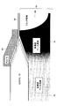
- FIG. 2 is an enlarged view of portion A in FIG. 1F (b).
- the lateral position of the LOCOS oxide film 170 may vary depending on the processing accuracy.
- the end portion of the LOCOS oxide film 170 has a cross-sectional shape with a sharp tip such as the apex of a triangle in which the film thickness decreases toward the outside. With such a shape, the film thickness slightly changes depending on the position of the end portion of the LOCOS oxide film 170 in the lateral direction, and the lateral size of the emitter region 160 is affected and fluctuates accordingly.
- the high-concentration base region 151 into which impurities are implanted by permeation of the LOCOS oxide film 170 is located below the portion of the LOCOS oxide film 170 where the triangular film thickness changes, so that the processing accuracy of the LOCOS oxide film 170 and The film thickness affects the impurity concentration.
- the impurity concentration of the high concentration base region 151 affects the diffusion length of the minority carriers injected from the emitter region 160 during the operation of the transistor.
- the low concentration base region 152 is implanted through the thick film portion of the LOCOS oxide film 170, the impurity concentration is lower than that of the high concentration base region 151. Further, since the low concentration base region 152 has a low impurity concentration, the diffusion length of the minority carriers is long.
- an object of the present invention is to provide a method for manufacturing a semiconductor device capable of uniformizing device characteristics and a semiconductor integrated circuit device having the semiconductor device manufactured by such a method by a simple process.
- a method of manufacturing a semiconductor device includes a step of forming a LOCOS oxide film in a predetermined region of a surface of a semiconductor substrate, and covering a boundary between the LOCOS oxide film and the surface of the semiconductor substrate.
- a semiconductor device or a semiconductor integrated circuit device having excellent characteristics and uniformity is provided.
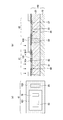
- FIG. 1A and 1B are views showing a LOCOS oxide film forming process according to an embodiment of the present invention, in which FIG. 1A is a plan view of a semiconductor substrate on which a semiconductor device is manufactured, and FIG. 4A and 4B are diagrams showing a high energy ion implantation process according to an embodiment of the present invention, in which FIG. 5A is a plan view of a bipolar transistor formation region, and FIG. 5B is a cross-sectional view of a semiconductor substrate. It is the figure which showed the heat processing process by one Example of this invention, (a) is a top view of a bipolar transistor formation area, (b) is sectional drawing of a semiconductor substrate.
- FIG. 4A and 4B are diagrams illustrating a gate oxide film forming process according to an embodiment of the present invention, in which FIG. 5A is a plan view of a bipolar transistor formation region, and FIG. 5B is a cross-sectional view of a semiconductor substrate.
- FIG. 5A and 4B are diagrams illustrating a polysilicon film forming process according to an embodiment of the present invention, in which FIG. 5A is a plan view of a bipolar transistor formation region, and FIG. 5B is a cross-sectional view of a semiconductor substrate. It is the figure which showed the ion implantation process by one Example of this invention, (a) is a top view of a bipolar transistor formation area, (b) is sectional drawing of a semiconductor substrate.
- 3A to 3G are diagrams showing a series of steps of a method for manufacturing a semiconductor device according to an embodiment of the present invention.
- FIG. 3A is a diagram showing a LOCOS oxide film forming step.
- 3A is a plan view of the semiconductor substrate 40 on which the semiconductor device is manufactured
- FIG. 3B is a cross-sectional view of the semiconductor substrate 40.
- the semiconductor substrate 40 includes a silicon substrate 10, an n-type layer 20, and a p-type layer 30.
- a LOCOS oxide film 70 is formed on the surface of the semiconductor substrate 40.
- the silicon substrate 10 may be a substrate made of another semiconductor material, but in this embodiment, an example using the silicon substrate 10 will be described.
- the n-type layer 20 may be formed by epitaxial growth.
- the surface of the semiconductor substrate 40 has a bipolar transistor formation region 41 and a MOS transistor formation region 42.
- the semiconductor device manufacturing method according to the present embodiment can manufacture a semiconductor device in which an impurity region is formed with high accuracy while utilizing a MOS transistor manufacturing process. Therefore, FIGS. 3A to 3G show an example in which an npn bipolar transistor is manufactured by the method of manufacturing a semiconductor device according to this embodiment and an n-channel MOS transistor is formed on the same semiconductor substrate 40.
- the semiconductor device manufacturing method according to the present embodiment can be used not only for the process of simultaneously manufacturing the MOS transistors but also for the device manufacturing alone, the MOS transistors need not always be manufactured at the same time. .
- a LOCOS oxide film 70 is formed on the surface of the semiconductor substrate 40 by the LOCOS method.
- the LOCOS oxide film 70 is formed at a position for isolating the bipolar transistor formation region 41 and the n-channel MOS transistor 42 from each other. Further, since the LOCOS oxide film 70 is also used as a mask at the time of ion implantation, it is provided in the bipolar transistor formation region 41 at a position where a high concentration impurity region is not formed.
- a p-type layer 30 is provided between the bipolar transistor formation region 41 and the MOS transistor formation region 42 in the vertical direction (depth direction) of the semiconductor substrate 40 in order to perform element isolation.
- the LOCOS oxide film 70 is formed on the surface of the semiconductor substrate 40, and the LOCOS oxide film 70 functions as an element isolation oxide film or a mask.
- the LOCOS oxide film 70 functions as an element isolation oxide film or a mask.
- FIGS. 3B to 3G only the bipolar transistor formation region 41 is shown in the plan view of FIG. 3A. Indicates.
- the semiconductor substrate 40 can be configured as a substrate made of various semiconductor materials as long as it is a semiconductor material.
- the semiconductor substrate 40 may be configured as a silicon substrate.
- the case where the semiconductor substrate 40 is an n-type conductivity will be described as an example.
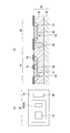
- FIG. 3B is a diagram showing a high energy ion implantation process. 3B, (a) is a plan view of the bipolar transistor formation region 41, and (b) is a cross-sectional view of the semiconductor substrate 40. FIG.
- a film-like resist 100 is applied to the surface (surface layer) of the semiconductor substrate 40, and ions are implanted.
- ions as impurities are implanted with high energy into the surface (surface layer) of the semiconductor substrate 40 to form the base region 50 and the p-type well layer 55.
- boron may be used as the ion.
- the base region 50 and the p-type well layer 55 which are p-type impurity regions are formed on the surface of the n-type semiconductor substrate 40.
- the resist 100 is selectively formed by patterning so as to cover portions of the semiconductor substrate 40 where the p-type impurity regions 50 and 55 are not formed.
- ions are implanted into the semiconductor substrate 40 with high energy to form the base region 50 and the p-type well layer 55. Since the ions are implanted with high energy, the ions pass through the LOCOS oxide film 70, A base region 50 and a p-type well layer 55 are also formed under the LOCOS oxide film 70.
- the high energy mentioned here means energy that allows ions implanted into the semiconductor substrate 40 to pass through the LOCOS oxide film 70 and form an impurity region under the LOCOS oxide film 70. The energy value can vary depending on the semiconductor substrate 40, the ion material, and the like.
- a resist 100 is formed in a frame shape, a LOCOS oxide film 70 functioning as a mask, and a base region in the opening 101 of the resist 100. 50 is exposed.
- FIG. 3C is a diagram showing a heat treatment process. 3C, (a) is a plan view of the bipolar transistor formation region 41, and (b) is a cross-sectional view of the semiconductor substrate 40. FIG.
- the semiconductor substrate 40 is subjected to a heat treatment to diffuse the impurities in the base region 50 and the p-type well layer 55, so that the impurity concentration distribution is uniform. Is achieved. Further, in the heat treatment step, the sizes of the base region 50 and the p-type well layer 55 are expanded laterally and downward.
- the base region 50 and the P-type well layer 55 are expanded laterally and downward in the semiconductor substrate 40.
- the high-concentration base region 51 and the high-concentration p-type well layer 56 are enlarged in the portion where the semiconductor substrate 40 is exposed, and the low-concentration base region 52 is located under the LOCOS oxide film 70.
- the low concentration p-type well layer 57 is enlarged.
- FIG. 3C (a) transparently shows a plan view of the bipolar transistor formation region 41.
- reference numerals in parentheses indicate regions that are transparently represented.
- the low-concentration base region 52 whose reference symbol is shown in parentheses is a transparently represented region.
- the exposed portion of the LOCOS oxide film 70 and the semiconductor substrate 40 is shown in the portion covered with the resist 100 in FIG.
- FIG. 3B (a) in the portion corresponding to the opening 101 of the resist 100, the portion where the LOCOS oxide film 70 is not formed becomes the high-concentration base region 51, and the LOCOS oxide film 70 is formed.
- the portion is a low concentration base region 52.
- the formation region of the base region 50 and the p-type well layer 55 is controlled by the presence or absence of the resist 100, and the impurity concentration in the base region 50 and the p-type well layer 55 is controlled by the presence or absence of the LOCOS oxide film 70.
- FIG. 3D is a diagram showing a gate oxide film forming step. 3D, (a) is a plan view of the bipolar transistor formation region 41, and (b) is a cross-sectional view of the semiconductor substrate 40. FIG.
- a gate oxide film 80 is formed on the exposed portions of the surfaces of the base region 50 and the p-type well layer 55.
- the gate oxide film 80 is a thin oxide film formed in the gate formation region in the MOS transistor manufacturing process.
- the thin gate oxide film 80 is formed not only in the MOS transistor formation region 42 but also in the bipolar transistor formation region 41.
- the gate oxide film may be composed of various materials, but may be composed of, for example, a SiO 2 film.
- the region where the gate oxide film 80 is formed is a portion where the surface of the semiconductor substrate 40 is exposed where the LOCOS oxide film 70 does not exist, the surface of the n-type layer 20, the high-concentration base region 51, or the high-concentration P-type. It becomes one of the well layers 56.
- FIG. 3D (a) shows a transparent plan view of the bipolar transistor formation region 41, which is substantially the same as FIG. 3C (a).
- the portion of the high-concentration base region 51 and the portion where the n-type layer 20 of the semiconductor substrate 40 is exposed are thin gate oxide films. Although it is covered with 80, if a figure is drawn transparently, it will become the same plane composition as (a) of Drawing 3C.
- the gate oxide film forming step shown in FIG. 3D may be omitted, for example, when the semiconductor device manufacturing method of this embodiment is used to manufacture a device alone without forming a MOS transistor at the same time.
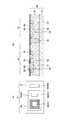
- FIG. 3E is a diagram showing a polysilicon film forming process. 3E, (a) is a plan view of the bipolar transistor formation region 41, and (b) is a cross-sectional view of the semiconductor substrate 40. FIG.
- a polysilicon film 90 is formed so as to cover the boundary.
- the polysilicon film 90 is used when forming a gate in the MOS transistor manufacturing process. Therefore, in the MOS transistor formation region 42, the polysilicon film 90 is formed as a gate.
- the polysilicon film 90 may be formed so as to cover the boundary between the LOCOS oxide film 70 and the surface of the semiconductor substrate 40 in the bipolar transistor formation region 41. .
- the polysilicon film 90 is formed to be used as a mask.
- the end portion of the LOCOS oxide film 70 has a shape in which the tip becomes thinner and the thickness becomes thinner as it approaches the tip, and the processing accuracy cannot be made high. Therefore, in the method of manufacturing the semiconductor device according to the present embodiment, the mask is formed with high accuracy using the polysilicon film 90 with high processing accuracy. Therefore, the end portion of the mask is not the LOCOS oxide film 70 but the polysilicon film 90, and the position of the mask end portion can be determined with high accuracy.
- Polysilicon is originally a material used as the gate of a MOS transistor, and the gate length and gate width of the MOS transistor are controlled with high precision, so that the polysilicon film 90 is formed with high precision processing. It becomes possible enough.
- the polysilicon film 90 covers the inclined portion of the LOCOS oxide film 70 and the gate oxide so as to cover the boundary between the LOCOS oxide film 70 and the gate oxide film 80 on the surface of the semiconductor substrate 40 where the emitter region 60 is to be formed. It is formed so as to straddle the film 80.
- the LOCOS oxide film 70 is used as it is in the central portion where the LOCOS oxide film 70 is sufficiently thick, and the inclined portion of the tip where the processing accuracy is lowered is covered with the polysilicon film 90, the minimum polysilicon is obtained.
- a functionally sufficient mask effect can be obtained by forming the film 90.
- the polysilicon film forming process is a process performed in a normal MOS transistor manufacturing process, there is no need to add an extra process to the MOS transistor manufacturing process in order to manufacture a bipolar transistor.
- a highly accurate mask can be formed with the same number of steps as in the manufacturing process.
- FIG. 3E shows a plan view of the bipolar transistor formation region 41.
- the planar configuration is such that the polysilicon film 90 surrounds the periphery of the high concentration base region 51.
- the other parts are the same as (a) of FIG.
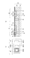
- FIG. 3F is a diagram showing an ion implantation process. 3F, (a) is a plan view of the bipolar transistor formation region 41, and (b) is a cross-sectional view of the semiconductor substrate 40. FIG.
- a resist 102 is selectively formed and patterned on the surface of the structure shown in FIG. 3E.
- An emitter region 60 that is an impurity region is formed on the surface of the high-concentration base region 51 of the base region 50.
- a drain region 62 and a source region 63 are formed on the surface of the p-type well layer 55.
- ions are implanted on the surface of the base region 50, and an impurity region (emitter region 60) is further formed.
- a collector contact region 61 is formed on the surface of the portion of the n-type layer 20 covered with the gate oxide film 80. If the formation of the gate oxide film 80 is omitted, the collector contact region 61 may be formed on the surface of the exposed portion of the n-type layer 20 in the bipolar transistor formation region 41.
- the resist 102 is patterned, and a portion where no impurity region is formed is covered with the resist 102.
- ions are implanted using the resist 102, the LOCOS oxide film 70, and the polysilicon film 90 as a mask.
- the LOCOS oxide film 70 is used as a part of the mask, ions are implanted with low energy that does not pass through the LOCOS oxide film 70.
- the portion of the semiconductor substrate 40 that is not covered with the LOCOS oxide film 70 is covered with a thin gate oxide film 80, so that the gate oxide film 80 has low energy to transmit and ions are implanted. It is.
- phosphorus may be used as the ions to be implanted.
- the emitter region 60, the collector contact region 61, the drain region 62, and the source region 63 are formed with the n-type conductivity type on the surfaces of the base region 50 and the p-type well layer 55. Note that since the drain region 62 and the source region 63 are the same impurity region, the arrangement may be reversed.
- the shape and size of the emitter region 60 are determined with high accuracy by the polysilicon film 90 functioning as a mask, and the emitter region 60 can be formed with high accuracy. Thereby, in the base region 50, the width of the high concentration base region 51 between the emitter region 60 and the low concentration base region 52 can be appropriately ensured.
- FIG. 3F shows a plan view of the bipolar transistor formation region 41.
- FIG. 3G is a diagram showing a heat treatment process.
- (a) is a plan view of the bipolar transistor formation region 41
- (b) is a cross-sectional view of the semiconductor substrate 40.
- the semiconductor substrate 40 is heat-treated after removing the resist 102.
- the emitter region 60, the collector contact region 61, the drain region 62, and the source region 63 formed on the surface of the semiconductor substrate 40 expand laterally and downward.
- the emitter region 60, the collector contact region 61, the drain region 62, and the source region 63 are formed thin on the surface of the semiconductor substrate 40 by low energy ion implantation, and compared with the base region 50 and the p-type well layer 55, The layer is considerably thin. Therefore, the lateral expansion amount due to the thermal diffusion is considerably smaller than that during the thermal diffusion of the base region 50, and the emitter region 60 does not dig into the high-concentration base region 51, and the end of the emitter region 60 is sufficiently covered. Can be controlled.
- the polysilicon film 90 in the bipolar transistor formation region 41 remains on the semiconductor substrate 40 as in the LOCOS oxide film 70, but the emitter region 60 and the base region 50 are separated by the gate oxide film 80. Since it is electrically disconnected and no voltage is applied, the operation of the bipolar transistor is not adversely affected.
- the polysilicon film 90 is formed and functions as a gate.
- FIG. 3G (a) transparently shows a plan view of the bipolar transistor formation region 41.
- the emitter region 60 whose surface is covered with the gate oxide film 80 is surrounded by the polysilicon film 90.
- a low concentration base region 52 is formed under the LOCOS oxide film 70.
- the portion where the high-concentration base region 51 is not covered with the polysilicon film 90 but only with the gate oxide film 80 is a base contact region. From here, current input to the base is performed.
- an npn bipolar transistor can be manufactured through a series of steps shown in FIGS. 3A to 3G.
- FIG. 4 is an enlarged view of portion B in FIG. 3G (b).
- a boundary portion between the emitter region 60 and the base region 50 of the completed bipolar transistor is shown.
- the mask is formed by the polysilicon film 90, so that the emitter region 60 is not affected by the LOCOS oxide film 70. It can be formed with high accuracy. Thereby, it is possible to avoid the end of the emitter region 60 from biting into the high-concentration base region 51, and to ensure a sufficient size in the lateral direction of the high-concentration base region 51.
- FIG. 5 is a diagram for explaining an operation example of the npn-type bipolar transistor according to the present embodiment.
- the npn-type bipolar transistor preferably has a normal operation in which the electrons of the minority carriers injected into the emitter region 60 move vertically and pass through the base region 50 and flow into the n-type layer 20 which is the collector region. Is the action.
- the width of the high-concentration base region 51 that surrounds the emitter region 60 from the side is small, the fractional carriers flow in the horizontal direction instead of the vertical direction.
- the high concentration base region 51 and the low concentration base region 52 have an impurity concentration gradient, the fractional carriers injected into the high concentration base region 51 are efficiently transferred to the low concentration base region 52. That is, a parasitic operation occurs.
- the width of the high concentration base region 51 is sufficiently long, it is possible to suppress the fractional carriers injected into the emitter region 60 from passing through the high concentration base region 51 and further moving to the low concentration base region 52. Parasitic operation can be prevented.
- the polysilicon film 90 with high processing accuracy covers the boundary between the LOCOS oxide film 70 and the surface of the semiconductor substrate 40, and an ion implantation process is performed using this as a mask, so that the end portion of the emitter region 60 is obtained. Is formed so as to face the end portions of the polysilicon film 90 and the LOCOS oxide film 70. Further, by defining the area of the emitter region 60 on the surface of the semiconductor substrate 40 with a mask of the polysilicon film 90 with high processing accuracy, the variation in the area of the emitter region 60 can be suppressed.
- the bipolar transistor can be operated vertically.
- a bipolar transistor having designed characteristics can be obtained.
- the bipolar transistor can be manufactured using the same process as that of the MOS transistor. Even when the bipolar transistor and the MOS transistor are manufactured on the same semiconductor substrate 40, the semiconductor device can be manufactured efficiently. it can.
- the semiconductor device manufactured by the method for manufacturing a semiconductor device according to this embodiment can be used for various electronic circuits, and can be configured as a reference voltage generation circuit, for example. Then, by housing the semiconductor device in a package, it can be configured as a semiconductor integrated circuit device. As a result, the semiconductor integrated circuit device having excellent characteristics in which the impurity regions are formed as designed and there is no variation can be obtained.
- CMOS complementary metal-oxide-semiconductor
- a polysilicon film with high processing accuracy can be used as a mask, and an impurity region can be formed with high accuracy by a simple manufacturing process.
- a semiconductor device manufacturing method is also used for a semiconductor device manufacturing process in which another impurity region is formed on the surface of an impurity region formed by high-energy ion implantation.
- another impurity region is formed on the surface of an impurity region formed by high-energy ion implantation.
- an active region of a transistor can be formed with high accuracy, and a transistor with favorable characteristics and less variation can be manufactured.
- a bipolar transistor with good characteristics and little variation can be manufactured.
- the present invention can be applied to a manufacturing process of a semiconductor device including a bipolar transistor and the like, and a semiconductor integrated circuit device using such a semiconductor device.
Landscapes
- Bipolar Transistors (AREA)
- Metal-Oxide And Bipolar Metal-Oxide Semiconductor Integrated Circuits (AREA)
- Bipolar Integrated Circuits (AREA)
Abstract
半導体装置の製造方法は、半導体基板の表面の所定領域に、LOCOS酸化膜を形成する工程と、該LOCOS酸化膜と前記半導体基板の表面の境界を覆うように、ポリシリコン膜を形成する工程と、該ポリシリコン膜をマスクとして、前記半導体基板の表面にイオンの打ち込みを行い、前記半導体基板の表面に、不純物領域を形成する工程とを含む。
Description
本発明は、半導体装置の製造方法及び半導体集積回路装置に関し、特に、半導体基板の表面の所定領域に、LOCOS酸化膜を形成する半導体装置の製造方法及びかかる方法により製造された半導体装置を有する半導体集積回路装置に関する。
従来から、半導体基板の表面に、LOCOS(Local Oxidation of Silicon)法によりLOCOS酸化膜を形成し、更にレジストを用いて、LOCOS酸化膜とレジストをマスクとしてイオンの打ち込みを行い、デバイスを形成する半導体装置の製造方法が知られている。
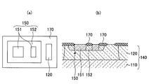
図1A乃至図1Fは、従来の半導体装置の製造方法の一例を示した図である。図1A乃至図1Fにおいては、npnトランジスタの製造方法の一例を説明する。図1A乃至図1Fのそれぞれにおいて(a)、(b)はそれぞれ平面図、断面図を示す。図1Aは、LOCOS酸化膜形成工程を示した図である。LOCOS酸化膜形成工程において、シリコン基板110上にn型層120が形成された半導体基板140の表面に、LOCOS法によりLOCOS酸化膜170が形成される。(a)の平面図に示すように、半導体基板140の表面のトランジスタ等のデバイスを形成する領域が、LOCOS酸化膜170で周囲を囲まれる。
図1Bは、ベース領域形成工程を示した図である。半導体基板140の不純物領域を形成しない部分は、レジスト200で覆われ、不純物領域を形成する部分は、レジスト200で覆われないで露出された状態となる。この、レジスト200がパターニングされた状態で、半導体基板140にイオンが打ち込まれ、不純物の注入が行われる。イオンは、例えば、ボロン等が用いられる。イオンは、高エネルギーで打ち込みが行われ、LOCOS酸化膜170のある部分は、LOCOS酸化膜170を透過してイオンが打ち込まれる。LOCOS酸化膜170の無い部分は、直接n型層120にイオンが打ち込まれる。半導体基板140のイオンが打ち込まれた箇所は、不純物が注入されたベース領域150となる。ベース領域150中、LOCOS酸化膜170が無く、半導体基板140のn型層120が露出した箇所は、高濃度ベース領域151となり、LOCOS酸化膜170の下の箇所は、低濃度ベース領域152となる。
図1Cは、熱処理工程を示した図である。図1Bにおいて、高エネルギーイオンの打ち込みが行われた後は、レジスト200が除去され、半導体基板140の加熱処理が行われる。これにより、ベース領域150の熱拡散が行われ、注入された不純物がベース領域150中を拡散し、不純物濃度の濃度分布が平均化の方向に向かうとともに、ベース領域150が側方及び下方に拡大する。
図1Dは、ゲート酸化膜形成工程を示した図である。ゲート酸化膜形成工程においては、高濃度ベース領域151が露出した部分に、ゲート酸化膜180が形成される。これにより、高濃度ベース領域151の表面は、ゲート酸化膜180に覆われる。なお、ゲート酸化膜180は、MOSトランジスタを製造するプロセスにおける、ゲート酸化膜180と同様の薄膜状の酸化膜という意味であり、必ずしもその領域にゲートを形成するという意味ではない。
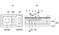
図1Eは、エミッタ領域形成工程を示した図である。エミッタ領域形成工程においては、半導体基板140のイオンの打ち込みを行わない箇所がレジスト202で覆われる。一方、イオンの打ち込みの際、有機物のレジスト202が削れてエミッタ領域160に混入すると、エミッタ領域160の特性に悪影響を与えるため、エミッタ領域160の端部は、LOCOS酸化膜170をマスクとしてイオンの打ち込みが行われる。イオンは、例えば、リンが用いられてよい。また、イオンの打ち込みは、ゲート酸化膜180の形成された領域に、LOCOS酸化膜170をマスクとして行われるため、ゲート酸化膜180を透過し、かつLOCOS酸化膜170を透過しない程度の低エネルギーで行われる。低エネルギーイオンの打ち込みにより、不純物領域であるベース領域150の表面に、やはり不純物領域であるエミッタ領域160が形成される。
図1Fは、熱処理工程を示した図である。熱処理工程においては、半導体基板140が加熱処理され、エミッタ領域160の熱拡散が行われる。これにより、エミッタ領域160の不純物濃度が平均化するとともに、エミッタ領域160が側方及び下方に拡大する。なお、n型層120は、コレクタ領域として機能し、npn型バイポーラトランジスタを形成することができる。なお、n型層120は、例えば、エピタキシャル成長により、P型のシリコン基板の上に形成されてもよい。
また、例えば、特許文献1には、MOS(Metal-Oxide-Semiconductor)トランジスタとバイポーラトランジスタが同一の半導体基板上に混載されているBiCMOS(Bipolar Complementary Metal-Oxide-Semiconductor)集積回路装置であって、バイポーラトランジスタは、ベース層に接続された、側面に絶縁体の側壁を有するベース引出電極を有し、当該絶縁体の側壁を用いて、エミッタ電極引出開口及びエミッタ層を自己整合的に形成したものが記載されている。
かかるBiCMOS集積回路装置の絶縁体の側壁の形成は、ベース引出電極上に絶縁膜を形成する工程と、ベース引出電極の側面及びベース引出電極に取り囲まれたエミッタ形成領域を含む半導体基板全体にTEOS膜の絶縁膜を成長させる工程と、TEOS膜の絶縁膜を異方性エッチングして、エミッタ形成領域上のベース引出電極側面に側壁を残す工程と、を含んでいる。
しかしながら、上述の図1A乃至図1Fの従来技術の構成では、エミッタ領域160のサイズが、LOCOS酸化膜170の加工精度及び膜厚に影響を受けてしまい、エミッタ領域160の変動により、隣接するデバイスの特性が不均一となるという問題があった。また、エミッタ領域160のサイズが大きくなると、ベース領域150の高濃度ベース領域151のサイズが小さくなり、バイポーラトランジスタを縦方向に動作させたいにも関わらず、横方向の寄生動作が発生するようになり、トランジスタ特性が悪化するとともにバラつきが生じてしまうという問題があった。
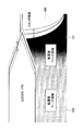
図2は、図1Fの(b)のA部分の拡大図である。図2に示すように、LOCOS酸化膜170の横方向の位置は、加工精度により変動するおそれがある。また、LOCOS酸化膜170の端部は、外側に向かうにつれて膜厚が減少する、三角形の頂点のような先端が尖った断面形状となっている。このような形状であると、LOCOS酸化膜170の端部の横方向の位置により、膜厚も微妙に変化し、エミッタ領域160の横方向の大きさもそれによって影響を受けて変動する。同様に、LOCOS酸化膜170の透過により不純物が注入される高濃度ベース領域151は、LOCOS酸化膜170の三角形状の膜厚が変化する部分の下方にあるため、LOCOS酸化膜170の加工精度及び膜厚が、その不純物濃度に影響を与える。
また、高濃度ベース領域151の不純物濃度は、トランジスタの動作中、エミッタ領域160から注入された小数キャリアの拡散長に影響を及ぼす。一方、低濃度ベース領域152は、LOCOS酸化膜170の厚膜部分を通して打ち込まれているので、高濃度ベース領域151よりも、不純物濃度が低い。また、低濃度ベース領域152は、不純物濃度が低いので、小数キャリアの拡散長が長い。このように、高濃度ベース領域151から低濃度ベース領域152にかけて、不純物の濃度勾配があるので、高濃度ベース領域151に注入された小数キャリアは、効率よく低濃度ベース領域152に移送され、トランジスタの横方向の寄生動作が大きくなってしまうという問題があった。
更に、特許文献1に記載の構成では、エミッタ領域を酸化膜の側壁で精度よく形成することは可能であるが、上述のように、複雑な工程を必要とし、製造工程が複雑化し、コスト増にも繋がるという問題があった。また、通常のMOSトランジスタの製造工程とは異なる工程が多く、バイポーラトランジスタを、MOSトランジスタの工程と同じ工程で製造することができず、工程数の増加に繋がるという問題があった。
そこで、本発明は、簡素な工程で、デバイスの特性を均一化することができる半導体装置の製造方法及びかかる方法により製造された半導体装置を有する半導体集積回路装置を提供することを目的とする。
本発明の一側面によれば、半導体装置の製造方法は、半導体基板の表面の所定領域に、LOCOS酸化膜を形成する工程と、該LOCOS酸化膜と前記半導体基板の表面の境界を覆うように、ポリシリコン膜を形成する工程と、該ポリシリコン膜をマスクとして、前記半導体基板の表面にイオンの打ち込みを行い、前記半導体基板の表面に、不純物領域を形成する工程と、を含む。
本発明の一側面によれば、特性が良好で均一な半導体装置又は半導体集積回路装置が提供される。
本発明の他の目的、特徴及び利点は添付の図面を参照し以下の詳細な説明を読むことにより、一層明瞭となるであろう。
従来の半導体装置の製造方法の一例におけるLOCOS酸化膜形成工程を示した図である。
従来の半導体装置の製造方法の一例におけるベース領域形成工程を示した図である。
従来の半導体装置の製造方法の一例における熱処理工程を示した図である。
従来の半導体装置の製造方法の一例におけるゲート酸化膜形成工程を示した図である。
従来の半導体装置の製造方法の一例におけるエミッタ領域形成工程を示した図である。
従来の半導体装置の製造方法の一例における熱処理工程を示した図である。
図1Fの(b)のA部分の拡大図である。
本発明の一実施例によるLOCOS酸化膜形成工程を示した図であり、(a)は半導体装置が製造される半導体基板の平面図、(b)は半導体基板の断面図である。
本発明の一実施例による高エネルギーイオン打ち込み工程を示した図であり、(a)はバイポーラトランジスタ形成領域の平面図、(b)は半導体基板の断面図である。
本発明の一実施例による熱処理工程を示した図であり、(a)はバイポーラトランジスタ形成領域の平面図、(b)は半導体基板の断面図である。
本発明の一実施例によるゲート酸化膜形成工程を示した図であり、(a)はバイポーラトランジスタ形成領域の平面図、(b)は半導体基板の断面図である。
本発明の一実施例によるポリシリコン膜形成工程を示した図であり、(a)はバイポーラトランジスタ形成領域の平面図、(b)は半導体基板の断面図である。
本発明の一実施例によるイオン打ち込み工程を示した図であり、(a)はバイポーラトランジスタ形成領域の平面図、(b)は半導体基板の断面図である。
本発明の一実施例による熱処理工程を示した図であり、(a)はバイポーラトランジスタ形成領域の平面図、(b)は半導体基板の断面図である。
本発明の一実施例による図3Gの(b)のBの部分を拡大した図である。
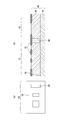
本発明の一実施例に係るnpn型バイポーラトランジスタの動作例を説明する図である。
以下、添付の図面を参照して、本発明の実施例を説明する。
図3A乃至図3Gは、本発明の実施例に係る半導体装置の製造方法の一連の工程を示した図である。
図3Aは、LOCOS酸化膜形成工程を示した図である。図3Aにおいて、(a)は半導体装置が製造される半導体基板40の平面図であり、(b)は半導体基板40の断面図である。
図3Aの(b)を参照すれば、半導体基板40は、シリコン基板10と、n型層20と、p型層30とを有する。また、半導体基板40の表面に、LOCOS酸化膜70が形成されている。シリコン基板10は、他の半導体材料からなる基板であってもよいが、本実施例においては、シリコン基板10を用いた例を挙げて説明する。n型層20は、例えば、エピタキシャル成長によって形成されてもよい。
半導体基板40の表面は、バイポーラトランジスタ形成領域41と、MOSトランジスタ形成領域42とを有している。本実施例に係る半導体装置の製造方法は、MOSトランジスタの製造工程を利用しつつ、高精度に不純物領域が形成された半導体装置を製造することができる。よって、図3A乃至図3Gにおいては、本実施例に係る半導体装置の製造方法によりnpn型バイポーラトランジスタを製造するとともに、nチャネルMOSトランジスタを同じ半導体基板40上に形成する例を示すこととする。但し、本実施例に係る半導体装置の製造方法は、MOSトランジスタを同時に製造する工程だけでなく、単独でデバイスの製造に用いることができるので、MOSトランジスタの製造は、必ずしも同時に行われる必要は無い。
図3Aの(b)に示すように、LOCOS酸化膜形成工程においては、LOCOS法により、半導体基板40の表面に、LOCOS酸化膜70が形成される。LOCOS酸化膜70は、バイポーラトランジスタ形成領域41と、nチャネルMOSトランジスタ42とを素子分離する位置に形成される。また、LOCOS酸化膜70は、イオン打ち込み時のマスクとしても用いられるため、バイポーラトランジスタ形成領域41内においては、高濃度の不純物領域を形成しない位置にも設けられている。なお、バイポーラトランジスタ形成領域41と、MOSトランジスタ形成領域42との間には、素子分離を行うべく、半導体基板40の縦方向(深さ方向)にp型層30が設けられている。
図3Aの(a)を参照すれば、半導体基板40の表面の大半がLOCOS酸化膜70で覆われ、LOCOS酸化膜70で覆われていない領域に、半導体基板40のn型層20が露出している。このように、LOCOS酸化膜形成工程においては、LOCOS酸化膜70が半導体基板40の表面に形成され、LOCOS酸化膜70が、素子分離酸化膜又はマスクとして機能する。なお、図3Aの(a)においては、バイポーラトランジスタ形成領域41の表面のみが示されており、図3B乃至図3Gにおいても同様に、(a)の平面図については、バイポーラトランジスタ形成領域41のみを示す。
また、半導体基板40は、半導体材料であれば、種々の半導体材料からなる基板として構成することができる。例えば、半導体基板40は、シリコン基板として構成されてもよい。また、本実施例に係る半導体装置の製造方法においては、半導体基板40が、n型の導電型である場合を例に挙げて説明することとする。
図3Bは、高エネルギーイオン打ち込み工程を示した図である。図3Bにおいて、(a)はバイポーラトランジスタ形成領域41の平面図であり、(b)は半導体基板40の断面図である。
図3Bの(b)を参照すれば、半導体基板40の表面(表層)に、膜状のレジスト100が塗布され、イオンが打ち込まれている。高エネルギーイオン打ち込み工程においては、半導体基板40の表面(表層)に、不純物であるイオンが高エネルギーで打ち込まれ、ベース領域50及びp型ウェル層55が形成される。イオンは、例えば、ボロンが用いられてもよい。この場合、n型の半導体基板40の表面に、p型不純物領域であるベース領域50及びp型ウェル層55が形成されることになる。レジスト100は、半導体基板40上のp型不純物領域50、55を形成しない部分を覆うように、パターニングされて選択的に形成される。
レジスト100の形成後は、半導体基板40にイオンを高エネルギーで打ち込み、ベース領域50及びp型ウェル層55を形成するが、イオンは高エネルギーで打ち込まれるため、LOCOS酸化膜70を透過して、LOCOS酸化膜70の下にもベース領域50及びp型ウェル層55が形成される。なお、ここで言う高エネルギーは、半導体基板40に打ち込まれたイオンが、LOCOS酸化膜70を透過してLOCOS酸化膜70の下に不純物領域を形成できる程のエネルギーという意味であり、具体的なエネルギー値は、半導体基板40やイオンの材質等により変化し得る。
ベース領域50内において、LOCOS酸化膜70で覆われていない、半導体基板40の表面が露出した部分は、不純物の濃度が高い高濃度ベース領域51となる。また、LOCOS酸化膜70に覆われたLOCOS酸化膜70の下方の部分は、低濃度ベース領域52となる。MOSトランジスタ形成領域42にも同様に、高濃度p型ウェル層56及び低濃度p型ウェル層57がp型ウェル層55内に形成される。
図3Bの(a)に示されるバイポーラトランジスタ形成領域41の平面図を参照すれば、枠状にレジスト100が形成され、レジスト100の開口101に、マスクとして機能するLOCOS酸化膜70と、ベース領域50が露出している。
図3Cは、熱処理工程を示した図である。図3Cにおいて、(a)はバイポーラトランジスタ形成領域41の平面図であり、(b)は半導体基板40の断面図である。
熱処理工程においては、高エネルギーイオン打ち込み工程で用いたレジスト100が除去された後、半導体基板40が加熱処理され、ベース領域50及びp型ウェル層55内の不純物を拡散させ、不純物濃度分布の均一化が図られる。また、熱処理工程において、ベース領域50及びp型ウェル層55の大きさが、側方及び下方に拡大される。
図3Cの(b)を参照すれば、図3Bの(b)と比較して、半導体基板40において、ベース領域50及びP型ウェル層55が横方向及び下方向に拡大している。図3Cの(b)に示すように、半導体基板40が露出した部分は、高濃度ベース領域51及び高濃度p型ウェル層56が拡大し、LOCOS酸化膜70の下方は、低濃度ベース領域52及び低濃度p型ウェル層57が拡大している。
図3Cの(a)は、バイポーラトランジスタ形成領域41の平面図を透過的に示している。なお、図面において括弧内の参照符号が、透過的に表された領域を示している。図3Cの(a)では、参照符号が括弧内に示される低濃度ベース領域52が、透過的に表された領域である。バイポーラトランジスタ形成領域41のうち、図3Bの(a)において、レジスト100で覆われていた部分には、LOCOS酸化膜70及び半導体基板40の露出部分が示されている。一方、図3Bの(a)において、レジスト100の開口101に該当した部分については、LOCOS酸化膜70が形成されていない部分は、高濃度ベース領域51となり、LOCOS酸化膜70が形成されていた部分は、低濃度ベース領域52となっている。
このように、レジスト100の有無により、ベース領域50及びp型ウェル層55の形成領域が制御され、LOCOS酸化膜70の有無により、ベース領域50及びp型ウェル層55内の不純物濃度が制御される。
図3Dは、ゲート酸化膜形成工程を示した図である。図3Dにおいて、(a)はバイポーラトランジスタ形成領域41の平面図であり、(b)は半導体基板40の断面図である。
ゲート酸化膜形成工程においては、ベース領域50及びp型ウェル層55の表面の露出部分に、ゲート酸化膜80が形成される。ゲート酸化膜80は、MOSトランジスタ製造工程において、ゲート形成領域に形成する薄膜状の酸化膜である。この、薄膜状のゲート酸化膜80を、MOSトランジスタ形成領域42だけでなく、バイポーラトランジスタ形成領域41にも形成する。なお、ゲート酸化膜は、種々の材料で構成されてよいが、例えば、SiO2膜で構成されてもよい。
また、ゲート酸化膜80を形成する領域は、LOCOS酸化膜70の存在しない、半導体基板40の表面が露出した部分であるので、n型層20の表面、高濃度ベース領域51又は高濃度P型ウェル層56のいずれかになる。
図3Dの(a)は、バイポーラトランジスタ形成領域41の透過的な平面図を示しているが、図3Cの(a)と略同様の図となる。図3Dの(a)を参照すれば、バイポーラトランジスタ形成領域41のうち、高濃度ベース領域51の部分と、半導体基板40のn型層20が露出した部分は、表面が薄膜状のゲート酸化膜80で覆われるが、透過的に図を描くと、図3Cの(a)と同様の平面構成となる。
なお、図3Dに示すゲート酸化膜形成工程は、例えば、本実施例の半導体装置の製造方法をMOSトランジスタを同時に形成せずデバイスを単独で製造するのに用いる場合には省略しても良い。
図3Eは、ポリシリコン膜形成工程を示した図である。図3Eにおいて、(a)はバイポーラトランジスタ形成領域41の平面図であり、(b)は半導体基板40の断面図である。
図3Eの(b)を参照すれば、バイポーラトランジスタ形成領域41において、LOCOS酸化膜70と半導体基板40のうちエミッタ領域60(図3Fを参照し後述)を形成する部分の表面のゲート酸化膜80との境界を覆うように、ポリシリコン膜90が形成されている。ポリシリコン膜90は、MOSトランジスタ製造工程において、ゲートを形成する際に用いる。よって、MOSトランジスタ形成領域42においては、ゲートとしてポリシリコン膜90が形成されている。
なお、ゲート酸化膜80の形成を省略する場合には、上記ポリシリコン膜90は、バイポーラトランジスタ形成領域41において、LOCOS酸化膜70と半導体基板40の表面との境界を覆うように形成されて良い。
一方、バイポーラトランジスタ形成領域41においては、ポリシリコン膜90は、マスクとして利用されるために形成される。図2を参照し説明したように、LOCOS酸化膜70の端部は、先端に接近するにつれて先が細くなって厚さが薄くなる形状であり、加工精度を高精度にすることができない。そこで、本実施例に係る半導体装置の製造方法においては、加工精度の高いポリシリコン膜90を用いて、高精度にマスクを形成している。よって、マスクの端部は、LOCOS酸化膜70ではなく、ポリシリコン膜90となり、マスク端部の位置を高精度に定めることができる。ポリシリコンは、本来的には、MOSトランジスタのゲートとして用いられる材料であり、MOSトランジスタのゲート長及びゲート幅は高精度に管理されているので、高精度な加工でポリシリコン膜90を形成することが、十分に可能となる。
このように、マスクの端部を、マスクとしての加工精度に問題があるLOCOS酸化膜70の端部の代わりに加工精度の高いポリシリコン膜90を用いて形成することにより、高精度にマスク形状を加工することができる。よって、ポリシリコン膜90は、LOCOS酸化膜70と半導体基板40のうちエミッタ領域60を形成する部分の表面のゲート酸化膜80との境界を覆うように、LOCOS酸化膜70の傾斜部分とゲート酸化膜80とに跨るように形成する。これにより、LOCOS酸化膜70の厚さが十分ある中央部分はそのままLOCOS酸化膜70を活かし、加工精度が低下する先端の傾斜部分をポリシリコン膜90で覆うようにすれば、最小限のポリシリコン膜90の形成で機能的に十分なマスク効果を得ることができる。
また、ポリシリコン膜形成工程は、通常のMOSトランジスタの製造プロセスで行われる工程であるから、バイポーラトランジスタを製造するために、MOSトランジスタの製造工程に余分な工程を追加する必要がなく、MOSトランジスタの製造プロセスと同じ工程数で高精度なマスクを形成することができる。
図3Eの(a)は、バイポーラトランジスタ形成領域41の平面図を示している。高濃度ベース領域51の周囲を、ポリシリコン膜90が囲むような平面構成となっている。その他の部分は、図3Dの(a)と同様であるので、説明を省略する。
図3Fは、イオン打ち込み工程を示した図である。図3Fにおいて、(a)はバイポーラトランジスタ形成領域41の平面図であり、(b)は半導体基板40の断面図である。
図3Fの(b)を参照すれば、図3Eに示す構造体の表面に、レジスト102が選択的に形成されてパターニングされている。また、ベース領域50の高濃度ベース領域51の表面に、不純物領域であるエミッタ領域60が形成されている。同様に、p型ウェル層55の表面には、ドレイン領域62及びソース領域63が形成されている。
イオン打ち込み工程においては、ベース領域50の表面に、イオンの打ち込みが行われ、更に不純物領域(エミッタ領域60)が形成される。また、バイポーラトランジスタ形成領域41において、n型層20のゲート酸化膜80に覆われた部分の表面には、コレクタコンタクト領域61が形成される。なお、ゲート酸化膜80の形成を省略する場合には、コレクタコンタクト領域61は、バイポーラトランジスタ形成領域41において、n型層20の露出した部分の表面に形成されて良い。
イオン打ち込み工程においては、ベース領域50の表面に、イオンの打ち込みが行われ、更に不純物領域(エミッタ領域60)が形成される。また、バイポーラトランジスタ形成領域41において、n型層20のゲート酸化膜80に覆われた部分の表面には、コレクタコンタクト領域61が形成される。なお、ゲート酸化膜80の形成を省略する場合には、コレクタコンタクト領域61は、バイポーラトランジスタ形成領域41において、n型層20の露出した部分の表面に形成されて良い。
イオン打ち込み工程においては、まず、レジスト102のパターニングが行われ、不純物領域を形成しない部分がレジスト102で覆われる。次いで、レジスト102と、LOCOS酸化膜70と、ポリシリコン膜90とをマスクとして、イオンの打ち込みが行われる。この場合、LOCOS酸化膜70をマスクの一部として用いるので、イオンは、LOCOS酸化膜70を透過しない程度の低エネルギーで打ち込まれる。また、半導体基板40のうち、LOCOS酸化膜70で覆われていない部分は、薄膜状のゲート酸化膜80で覆われているので、ゲート酸化膜80は透過するレベルの低エネルギーで、イオンは打ち込まれる。打ち込まれるイオンは、例えば、リンが用いられてもよい。これにより、エミッタ領域60、コレクタコンタクト領域61、ドレイン領域62及びソース領域63が、ベース領域50及びp型ウェル層55の表面にn型の導電型で形成されることになる。なお、ドレイン領域62とソース領域63は、同じ不純物領域であるので、配置が逆であってもよい。
エミッタ領域60の形状及び大きさは、マスクとして機能するポリシリコン膜90により高精度に定められ、エミッタ領域60を高精度に形成することができる。これにより、ベース領域50において、エミッタ領域60と低濃度ベース領域52の間の、高濃度ベース領域51の横幅の大きさを適切に確保することができる。
図3Fの(a)は、バイポーラトランジスタ形成領域41の平面図を示しているが、レジスト102と、LOCOS酸化膜70と、ポリシリコン膜90により形成されるマスクを用いイオンの打ち込みを行うことにより、エミッタ領域60が形成されている。
図3Gは、熱処理工程を示した図である。図3Gにおいて、(a)はバイポーラトランジスタ形成領域41の平面図であり、(b)は半導体基板40の断面図である。
熱処理工程においては、レジスト102を除去した後、半導体基板40が加熱処理される。これにより、図3Gの(b)に示すように、半導体基板40の表面に形成されたエミッタ領域60、コレクタコンタクト領域61、ドレイン領域62及びソース領域63が側方及び下方に拡大する。
なお、エミッタ領域60、コレクタコンタクト領域61、ドレイン領域62及びソース領域63は、低エネルギーのイオン打ち込みにより半導体基板40の表面に薄く形成され、ベース領域50及びp型ウェル層55と比較して、厚さが相当に薄い層である。よって、熱拡散による側方への拡大量は、ベース領域50の熱拡散時に比較して相当に小さくなり、エミッタ領域60は高濃度ベース領域51に大きく食い込まず、エミッタ領域60の端部を十分に制御することができる。
また、バイポーラトランジス形成領域41のポリシリコン膜90は、LOCOS酸化膜70と同様に、半導体基板40上に残されたままとなるが、ゲート酸化膜80によりエミッタ領域60及びベース領域50とは、電気的に断線されており、電圧が印加される訳ではないので、何らバイポーラトランジスタの動作に悪影響は及ぼさない。また、MOSトランジスタ形成領域42においては、ポリシリコン膜90は、ゲートとして形成され、機能することになる。
図3Gの(a)は、バイポーラトランジスタ形成領域41の平面図を透過的に示している。図3Gの(a)を参照すれば、ゲート酸化膜80で表面を覆われたエミッタ領域60が、ポリシリコン膜90に周囲が囲まれている。また、LOCOS酸化膜70の下には、低濃度ベース領域52が形成されている。なお、高濃度ベース領域51が、ポリシリコン膜90に覆われず、ゲート酸化膜80にのみ覆われた部分は、ベースコンタクト領域である。ここから、ベースへの電流入力を行うことになる。
このように、本実施例に係る半導体装置の製造方法においては、図3A乃至図3Gに示した一連の工程を経て、npn型バイポーラトランジスタを製造することができる。
図4は、図3Gの(b)のBの部分を拡大した図である。図4において、完成したバイポーラトランジスタのエミッタ領域60と、ベース領域50の境界部分が示されている。図4に示すように、LOCOS酸化膜70の横方向の位置が変動しても、ポリシリコン膜90によりマスクが形成されているので、LOCOS酸化膜70の影響を受けず、エミッタ領域60を高精度に形成することができる。これにより、エミッタ領域60の端部が高濃度ベース領域51に食い込むことを回避することができ、高濃度ベース領域51の横方向の大きさを十分に確保することができる。
図5は、本実施例に係るnpn型バイポーラトランジスタの動作例を説明するための図である。図5において、npn型バイポーラトランジスタは、エミッタ領域60に注入された小数キャリアの電子が、縦に移動してベース領域50を通過し、コレクタ領域であるn型層20に流れ込む動作が好ましい正常な動作である。しかしながら、エミッタ領域60を側方から囲んでいる高濃度ベース領域51の幅が小さいと、小数キャリアが縦方向ではなく、横方向に流れてしまう。また、高濃度ベース領域51と、低濃度ベース領域52は、不純物の濃度勾配があるので、高濃度ベース領域51に注入された小数キャリアは、効率良く低濃度ベース領域52に移送される。つまり、寄生動作をしてしまう。
一方、高濃度ベース領域51の幅が十分に長ければ、エミッタ領域60に注入された小数キャリアが高濃度ベース領域51を通過し、更に低濃度ベース領域52に移動することを抑制することができ、寄生動作を防止することができる。
図4に戻る。図4に示すように、加工精度の高いポリシリコン膜90で、LOCOS酸化膜70と半導体基板40の表面の境界を覆い、これをマスクとしてイオン打ち込み工程を行うことにより、エミッタ領域60の端部が、ポリシリコン膜90及びLOCOS酸化膜70の端部に対向するように形成される。また、加工精度の高いポリシリコン膜90のマスクで半導体基板40の表面におけるエミッタ領域60の面積を規定することにより、エミッタ領域60の面積のバラツキを抑えることができる。また、エミッタ領域60の端部を設計通りに規定して加工することにより、エミッタ領域60を側方から囲んでいる高濃度ベース領域51の横方向の長さ(寸法)を大きくし、バイポーラトランジスタを縦方向に動作させることができる。これにより、設計通りの特性を有するバイポーラトランジスタとすることができる。更に、バイポーラトランジスタは、MOSトランジスタと同様の工程を用いて製造することができ、同一の半導体基板40上にバイポーラトランジスタとMOSトランジスタを製造する場合にも、効率的に半導体装置を製造することができる。
なお、本実施例に係る半導体装置の製造方法により製造された半導体装置は、種々の電子回路に利用することができ、例えば、基準電圧生成回路として構成することができる。そして、半導体装置をパッケージに収容することにより、半導体集積回路装置として構成することができる。これにより、不純物領域が設計通りに形成され、バラツキの無い優れた特性を有する半導体集積回路装置とすることができる。
また、本実施例においては、半導体装置として、npn型バイポーラトランジスタを製造する例を挙げて説明したが、LOCOS酸化膜70をマスクとしてイオン打ち込み工程を実行する半導体製造工程であれば、種々の半導体装置の製造工程に適用することができる。また、MOSトランジスタ形成領域42には、CMOSを製造するようにしてもよい。CMOSの製造工程も、MOSトランジスタの製造工程と同様であるので、本実施例を同様に適用することができる。
本発明の一側面によれば、加工精度の高いポリシリコン膜をマスクとして利用することができ、簡素な製造工程で高精度に不純物領域を形成することができる。
本発明の一側面によれば、一実施例による半導体装置の製造方法を、高エネルギーイオン打ち込みにより形成された不純物領域の表面に、更に別の不純物領域を形成する半導体装置の製造工程にも利用することができ、種々の半導体装置について高精度な不純物領域の形成を行うことができる。
本発明の一側面によれば、トランジスタの活性領域を高精度に形成することができ、特性が良好でバラツキの少ないトランジスタを製造することができる。
本発明の一側面によれば、特性が良好でバラツキの少ないバイポーラトランジスタを製造することができる。
本発明の一側面によれば、MOSトランジスタを製造するプロセスを利用しつつ、余分な工程を増やすことなく、特性が良好でバラツキの少ない半導体装置を製造することができる。
本発明の一側面によれば、特性が良好でバラツキの少ない半導体集積回路装置を提供することができる。
本発明は具体的に開示された実施例に限定されることなく、本発明の範囲を逸脱することなく様々な変形例、改良例がなされるであろう。
本願は2009年7月13日に出願した日本国特許出願第2009-165084号に基づきその優先権を主張するものであり、同日本国出願の全内容を参照することにより本願に援用する。
本発明は、バイポーラトランジスタ等を含む半導体装置の製造工程や、かかる半導体装置を用いる半導体集積回路装置に適用することができる。
10、110 シリコン基板
20、120 n型層
30 p型層
40、140 半導体基板
41 バイポーラトランジスタ形成領域
42 MOSトランジスタ形成領域
50、150 ベース領域
51、151 高濃度ベース領域
52、152 低濃度ベース領域
60、160 エミッタ領域
61 コレクタコンタクト領域
62 ドレイン領域
63 ソース領域
70、170 LOCOS酸化膜
80、180 ゲート酸化膜
90 ポリシリコン膜
100、102、200、202 レジスト
20、120 n型層
30 p型層
40、140 半導体基板
41 バイポーラトランジスタ形成領域
42 MOSトランジスタ形成領域
50、150 ベース領域
51、151 高濃度ベース領域
52、152 低濃度ベース領域
60、160 エミッタ領域
61 コレクタコンタクト領域
62 ドレイン領域
63 ソース領域
70、170 LOCOS酸化膜
80、180 ゲート酸化膜
90 ポリシリコン膜
100、102、200、202 レジスト
Claims (9)
- 半導体基板の表面の所定領域に、LOCOS酸化膜を形成する工程と、
該LOCOS酸化膜と前記半導体基板の表面の境界を覆うように、ポリシリコン膜を形成する工程と、
該ポリシリコン膜をマスクとして、前記半導体基板の表面にイオンの打ち込みを行い、前記半導体基板の表面に、不純物領域を形成する工程と、を含む半導体装置の製造方法。 - 前記LOCOS酸化膜形成工程と前記ポリシリコン形成工程との間に、イオンが前記LOCOS酸化膜を透過するエネルギーによりイオン打ち込みを行う工程を含む請求項1に記載の半導体装置の製造方法。
- 前記不純物領域は、トランジスタの活性領域である請求項1に記載の半導体装置の製造方法。
- 前記トランジスタは、バイポーラトランジスタである請求項3に記載の半導体装置の製造方法。
- 前記バイポーラトランジスタは、npn型トランジスタであって、
前記活性領域は、エミッタ領域である請求項4に記載の半導体装置の製造方法。 - 前記エミッタ領域の端部は、前記LOCOS酸化膜の端部と対向している請求項5に記載の半導体装置の製造方法。
- 前記半導体基板の表面の前記所定領域外に、前記LOCOS酸化膜を形成する工程において、MOSトランジスタの形成領域を定めるLOCOS酸化膜を更に形成し、
前記ポリシリコン膜を形成する工程において、前記MOSトランジスタのゲートを形成し、
前記不純物領域を形成する工程において、前記MOSトランジスタのドレイン領域及びソース領域を形成し、前記所定領域外にMOSトランジスタを同時に形成する請求項1に記載の半導体装置の製造方法。 - 前記MOSトランジスタは、CMOSである請求項7に記載の半導体装置の製造方法。
- 請求項3に記載のトランジスタを用いて構成した基準電圧生成回路を含む半導体集積回路装置。
Applications Claiming Priority (2)
| Application Number | Priority Date | Filing Date | Title |
|---|---|---|---|
| JP2009-165084 | 2009-07-13 | ||
| JP2009165084A JP2011023429A (ja) | 2009-07-13 | 2009-07-13 | 半導体装置の製造方法及び半導体集積回路装置 |
Publications (1)
| Publication Number | Publication Date |
|---|---|
| WO2011007699A1 true WO2011007699A1 (ja) | 2011-01-20 |
Family
ID=43449308
Family Applications (1)
| Application Number | Title | Priority Date | Filing Date |
|---|---|---|---|
| PCT/JP2010/061480 Ceased WO2011007699A1 (ja) | 2009-07-13 | 2010-07-06 | 半導体装置の製造方法及び半導体集積回路装置 |
Country Status (2)
| Country | Link |
|---|---|
| JP (1) | JP2011023429A (ja) |
| WO (1) | WO2011007699A1 (ja) |
Citations (8)
| Publication number | Priority date | Publication date | Assignee | Title |
|---|---|---|---|---|
| JPH04229648A (ja) * | 1990-07-30 | 1992-08-19 | Nippon Motoroola Kk | 所定のエミッタ領域を有するトランジスタおよびその製作方法 |
| JP2001144189A (ja) * | 1999-11-17 | 2001-05-25 | Nec Ic Microcomput Syst Ltd | 半導体集積回路装置及びその製造方法 |
| JP2003174100A (ja) * | 2001-12-05 | 2003-06-20 | Hitachi Ltd | 半導体装置およびその製造方法 |
| WO2005062150A1 (ja) * | 2003-12-24 | 2005-07-07 | Renesas Technology Corp. | 電圧発生回路と半導体集積回路装置 |
| JP2005533372A (ja) * | 2002-07-09 | 2005-11-04 | インピンジ インコーポレイテッド | フローティング・ゲート半導体構造 |
| JP2006059841A (ja) * | 2004-08-17 | 2006-03-02 | Nec Electronics Corp | 半導体装置及び半導体装置の製造方法 |
| JP2006222329A (ja) * | 2005-02-14 | 2006-08-24 | Elpida Memory Inc | 半導体装置 |
| JP2009088189A (ja) * | 2007-09-28 | 2009-04-23 | Sanyo Electric Co Ltd | Dmosトランジスタ及びその製造方法 |
-
2009
- 2009-07-13 JP JP2009165084A patent/JP2011023429A/ja active Pending
-
2010
- 2010-07-06 WO PCT/JP2010/061480 patent/WO2011007699A1/ja not_active Ceased
Patent Citations (8)
| Publication number | Priority date | Publication date | Assignee | Title |
|---|---|---|---|---|
| JPH04229648A (ja) * | 1990-07-30 | 1992-08-19 | Nippon Motoroola Kk | 所定のエミッタ領域を有するトランジスタおよびその製作方法 |
| JP2001144189A (ja) * | 1999-11-17 | 2001-05-25 | Nec Ic Microcomput Syst Ltd | 半導体集積回路装置及びその製造方法 |
| JP2003174100A (ja) * | 2001-12-05 | 2003-06-20 | Hitachi Ltd | 半導体装置およびその製造方法 |
| JP2005533372A (ja) * | 2002-07-09 | 2005-11-04 | インピンジ インコーポレイテッド | フローティング・ゲート半導体構造 |
| WO2005062150A1 (ja) * | 2003-12-24 | 2005-07-07 | Renesas Technology Corp. | 電圧発生回路と半導体集積回路装置 |
| JP2006059841A (ja) * | 2004-08-17 | 2006-03-02 | Nec Electronics Corp | 半導体装置及び半導体装置の製造方法 |
| JP2006222329A (ja) * | 2005-02-14 | 2006-08-24 | Elpida Memory Inc | 半導体装置 |
| JP2009088189A (ja) * | 2007-09-28 | 2009-04-23 | Sanyo Electric Co Ltd | Dmosトランジスタ及びその製造方法 |
Also Published As
| Publication number | Publication date |
|---|---|
| JP2011023429A (ja) | 2011-02-03 |
Similar Documents
| Publication | Publication Date | Title |
|---|---|---|
| US7122876B2 (en) | Isolation-region configuration for integrated-circuit transistor | |
| JP5925740B2 (ja) | トンネル電界効果トランジスタ | |
| JP3394408B2 (ja) | 半導体装置及びその製造方法 | |
| JP2010062564A (ja) | ポリエミッタ型バイポーラトランジスタ、bcd素子、ポリエミッタ型バイポーラトランジスタの製造方法及びbcd素子の製造方法 | |
| US20120267724A1 (en) | Mos semiconductor device and methods for its fabrication | |
| CN100552975C (zh) | 半导体装置及其制造方法 | |
| US9704967B2 (en) | Heterojunction bipolar transistor | |
| JP2009526409A (ja) | 絶縁体上に半導体が設けられた構造(soi)を有するボディコンタクト素子の形成方法及び装置 | |
| US8877575B2 (en) | Complementary junction field effect transistor device and its gate-last fabrication method | |
| KR102424771B1 (ko) | 반도체 소자 및 그 제조 방법 | |
| JPH1084045A (ja) | 半導体集積回路装置およびその製造方法 | |
| JPH08125180A (ja) | 半導体装置およびその製造方法 | |
| KR20100079381A (ko) | 반도체소자 및 그 제조방법 | |
| KR100997679B1 (ko) | 바이폴라 트랜지스터와 그 형성 방법 | |
| US6905935B1 (en) | Method for fabricating a vertical bipolar junction transistor | |
| WO2011007699A1 (ja) | 半導体装置の製造方法及び半導体集積回路装置 | |
| CN112466950A (zh) | 一种抗边缘漏电soi mos结构及其形成方法 | |
| JP6969543B2 (ja) | 半導体装置、cmos回路及び電子機器 | |
| JPH11340242A (ja) | ラテラルトランジスタおよびその製造方法 | |
| CN112466951B (zh) | 一种mos器件及避免mos器件寄生晶体管开启的方法 | |
| CN101257043A (zh) | 半导体装置及其制造方法 | |
| KR100925642B1 (ko) | 바이폴라 트랜지스터의 제조방법 | |
| KR101044325B1 (ko) | 표준 cmos 공정을 이용한 바이씨모스 소자 및 그 제조방법 | |
| JP2023073323A (ja) | 半導体装置及びトランジスタ | |
| JPH0438834A (ja) | Mosトランジスタの製造方法 |
Legal Events
| Date | Code | Title | Description |
|---|---|---|---|
| 121 | Ep: the epo has been informed by wipo that ep was designated in this application |
Ref document number: 10799758 Country of ref document: EP Kind code of ref document: A1 |
|
| NENP | Non-entry into the national phase |
Ref country code: DE |
|
| 122 | Ep: pct application non-entry in european phase |
Ref document number: 10799758 Country of ref document: EP Kind code of ref document: A1 |