WO2011004649A1 - アンテナ装置 - Google Patents
アンテナ装置 Download PDFInfo
- Publication number
- WO2011004649A1 WO2011004649A1 PCT/JP2010/057785 JP2010057785W WO2011004649A1 WO 2011004649 A1 WO2011004649 A1 WO 2011004649A1 JP 2010057785 W JP2010057785 W JP 2010057785W WO 2011004649 A1 WO2011004649 A1 WO 2011004649A1
- Authority
- WO
- WIPO (PCT)
- Prior art keywords
- antenna
- soldering
- antenna device
- pattern portion
- ground pattern
- Prior art date
- Legal status (The legal status is an assumption and is not a legal conclusion. Google has not performed a legal analysis and makes no representation as to the accuracy of the status listed.)
- Ceased
Links
Images



Classifications
-
- H—ELECTRICITY
- H01—ELECTRIC ELEMENTS
- H01Q—ANTENNAS, i.e. RADIO AERIALS
- H01Q1/00—Details of, or arrangements associated with, antennas
- H01Q1/36—Structural form of radiating elements, e.g. cone, spiral, umbrella; Particular materials used therewith
- H01Q1/38—Structural form of radiating elements, e.g. cone, spiral, umbrella; Particular materials used therewith formed by a conductive layer on an insulating support
-
- H—ELECTRICITY
- H01—ELECTRIC ELEMENTS
- H01Q—ANTENNAS, i.e. RADIO AERIALS
- H01Q1/00—Details of, or arrangements associated with, antennas
- H01Q1/12—Supports; Mounting means
- H01Q1/22—Supports; Mounting means by structural association with other equipment or articles
- H01Q1/24—Supports; Mounting means by structural association with other equipment or articles with receiving set
- H01Q1/241—Supports; Mounting means by structural association with other equipment or articles with receiving set used in mobile communications, e.g. GSM
- H01Q1/242—Supports; Mounting means by structural association with other equipment or articles with receiving set used in mobile communications, e.g. GSM specially adapted for hand-held use
- H01Q1/243—Supports; Mounting means by structural association with other equipment or articles with receiving set used in mobile communications, e.g. GSM specially adapted for hand-held use with built-in antennas
-
- H—ELECTRICITY
- H01—ELECTRIC ELEMENTS
- H01Q—ANTENNAS, i.e. RADIO AERIALS
- H01Q9/00—Electrically-short antennas having dimensions not more than twice the operating wavelength and consisting of conductive active radiating elements
- H01Q9/04—Resonant antennas
- H01Q9/0407—Substantially flat resonant element parallel to ground plane, e.g. patch antenna
- H01Q9/0421—Substantially flat resonant element parallel to ground plane, e.g. patch antenna with a shorting wall or a shorting pin at one end of the element
Definitions
- the present invention relates to an antenna device, and more particularly, to an antenna device used in a frequency band of a wireless LAN (Local Area Network).
- a wireless LAN Local Area Network
- a wireless LAN refers to a LAN that uses a transmission path other than a wired cable, such as radio waves and infrared rays.
- the standardization of wireless LAN has been formulated by the 802.11 committee of the IEEE (American Institute of Electrical and Electronics Engineers). That is, the IEEE 802.11 committee has established standards and specifications for wireless LAN standards.
- IEEE 802.11a is a 5 GHz band high-speed wireless LAN / wireless access standard formulated by the IEEE 802.11 committee.
- the communication speed (transfer speed) is about 20 to 50 Mbit / sec.
- CSMA / CD carrier ⁇ ⁇ multiple access with collision detection
- MAC medium access control
- the modulation method of the physical layer is OFDM (Orthogonal Frequency Division Multiplexing).
- IEEE 802.11b is a wireless LAN specification standardized in September 1999 by the IEEE 802.11 committee. IEEE 802.11b uses a 2.4 GHz band frequency and uses direct spreading (DS) as a modulation method.
- the transmission rate (transfer rate) is 11 Mbit / sec and 5.5 Mbit / sec.
- IEEE 802.11g is one of the wireless LAN standards established by the IEEE 802.11 Committee in June 2003, and is a specification that performs communication at about 54 Mbit / s in the 2.4 GHz band. . OFDM is adopted as the modulation method. Therefore, IEEE802.11g uses the same 2.4 GHz band frequency as IEEE802.11b, and supports a transfer rate of 54 Mbit / s, which is about five times that of IEEE802.11b. Unlike IEEE 802.11a, which also supports a transfer rate of 54 Mbit / s, IEEE 802.11g is also compatible with IEEE 802.11b.
- the maximum transfer rate of 54 Mbit / s is exactly the same as that of IEEE 802.11a, but the 2.4 GHz band is a “congested” frequency band that is used in many devices other than wireless LAN. For this reason, it is said that the actual transfer rate in IEEE 802.11g is slower than that in IEEE 802.11a.
- IEEE 802.11b and IEEE 802.11g use the same 2.4 GHz band, they are collectively referred to as IEEE 802.11b / g here.
- Patent Document 1 discloses a plane polarized antenna that can be easily downsized and mounted.
- the plane polarized antenna disclosed in Patent Document 1 includes a flat plate insulating substrate and a conductor portion provided on the flat plate insulating substrate.
- the conductor portion includes an inverted F antenna portion having a feeding point and a ground surface portion.
- the core wire (center conductor) of the coaxial cable is connected to the feeding point of the inverted F antenna portion, and the ground wire (external conductor) of the coaxial cable is connected to the ground plane portion.
- Patent Document 2 discloses a planar antenna that can secure stable communication and is excellent in space efficiency.
- an element, a ground plate, and a short-circuit portion are arranged on an insulating base material, and power is supplied through a strip line formed on the other surface of the insulating base material.
- a stripline has a start point and an end point. The start point of the strip line forms one through hole provided in the insulating base material, and the end point of the strip line forms another through hole provided in the insulating base material.
- the inner conductor of the feeding coaxial cable is connected to the start point of the strip line, and the feeding point of the element is connected to the end point of the strip line.
- the outer conductor of the power feeding coaxial cable is connected to the ground point of the ground plate.
- the antenna devices disclosed in Patent Documents 1 and 2 described above are called “substrate antennas” because the antenna pattern is formed on the substrate.
- Patent Document 3 discloses a broadband and high gain antenna.
- the antenna disclosed in Patent Literature 3 is formed with an antenna element provided with at least one bent portion, a ground portion to which one end of the antenna element is connected, and a direction in which the inner angle of the bent portion is divided from the bent portion. It has a feed part and a feed line connected to this feed part.
- An internal conductor of a coaxial cable that is a feed line is connected to the feed unit.
- the outer conductor of the coaxial cable is connected to the ground portion.
- a flat plate made of phosphor bronze or the like is pressed to form a conductive flat plate in which a power feeding portion is provided in the antenna element, the ground portion, and the bent portion of the antenna element.
- An antenna using such a conductive flat plate is called a “sheet metal antenna”.
- Patent Document 4 discloses a connection structure between an antenna and a communication cable that can prevent a shift in transmission / reception frequency and improve connection workability when the antenna and the communication cable are connected by soldering or the like.
- the antenna includes an antenna element made of a metal member and an insulating layer provided on at least a part of the surface of the antenna element. Two window holes are formed in the insulating layer. The antenna element and the conductor portion of the communication cable are connected through these window holes.
- the antenna element includes a radiation conductor part, a ground conductor part, a short-circuit conductor part, and a feed path.
- the ground conductor is rectangular.
- the communication cable has an inner conductor and an outer conductor. The ground conductor portion and the external conductor are connected using solder through the first window hole, and the power supply path and the internal conductor are connected using solder through the second window hole.
- the communication cable extends in parallel with the longitudinal direction of the antenna element.
- Patent Document 5 discloses a multi-frequency antenna that is small, lightweight, and has a wide tuning frequency band.
- the multi-frequency antenna disclosed in Patent Document 5 includes an antenna element extending in the X-axis direction, a ground plate electrically connected to the antenna element via a short-circuit line, and extending in parallel with the longitudinal direction of the antenna element. And a coaxial cable disposed between the antenna element and the ground plate.
- a feed line extends from the feed point of the antenna element.
- the ground plate has a protruding piece protruding toward the antenna element.
- the central conductor of the coaxial cable is connected to the feed line, and the outer conductor of the coaxial cable is connected to the protruding piece.
- Japanese Laid-Open Patent Publication No. 2008-187631 Japanese Unexamined Patent Publication No. 2005-136784 Japanese Laid-Open Patent Publication No. 2007-159064 Japanese Unexamined Patent Publication No. 2004-173143 Japanese Unexamined Patent Publication No. 2005-142739
- soldering is performed as follows. Using a soldering iron, heat is applied to a specific part of the ground plate (ground pattern part) (that is, a part where soldering is performed), and the temperature of the specific part is increased to the soldering temperature or higher. As a result, the solder is melted to connect the outer conductor of the coaxial cable and the ground plate (ground pattern portion). That is, it is necessary to heat the part (specific part) where soldering is performed to the soldering temperature or higher.
- Patent Documents 1 to 5 described above there are problems as described below.
- the outer conductor of the coaxial cable is connected to the protruding piece of the ground plate. Since this protruding piece is very small, it may be peeled off from the ground plate. As described above, since the peel strength is weak, there is a possibility that distortion occurs in the antenna pattern.
- an object of the present invention is to provide an antenna device capable of easily soldering an outer conductor of a coaxial cable to a ground pattern portion.
- an antenna device (10; 10A) capable of transmitting and receiving radio waves, a coaxial cable (20) having a central conductor (22) and an outer conductor (21), and an antenna element (30; 30A).
- the antenna element (30; 30A) includes an antenna pattern part (32; 32A) and a ground pattern part (34; 34A), and the coaxial cable (
- the central conductor (22) of 20) is soldered (51) and electrically connected to the first soldering portion (324; 324A) of the antenna pattern portion (32; 32A), and the coaxial cable (20).
- the outer conductor (21) is soldered (52) and electrically connected to the second soldering portion (344; 344A) of the ground pattern portion (34; 34A), and
- the patterned portion (34; 34A) has an opening (34a; 34Aa) that defines a second soldering portion (344; 344A), and the second soldering portion (344; 344A) includes:
- An antenna device (10; 10A) is obtained, which is arranged between the first soldering portion (324; 324A) and the opening (34a; 34Aa).
- the coaxial cable (20) is arranged on the ground pattern portion (32; 32A) in a direction orthogonal to the extending direction (Y) of the antenna pattern portion (32; 32A) ( X) and may extend parallel to one side of the ground pattern portion (34; 34A).
- the predetermined frequency band may be a 2.4 GHz band frequency, for example.
- the antenna pattern portion (32; 32A) may be composed of, for example, an inverted F antenna.
- the central conductor (22) of the coaxial cable (20) is connected to the feeding portion (324; 324A) of the inverted F antenna as the first soldering portion.
- the antenna pattern portion (32) and the ground pattern portion (34) are formed on the main surface (31u) of the substrate (31). It is comprised from the conductor foil made.
- the conductor foil is made of, for example, copper foil.
- the antenna element (30A) is made of a metal plate.
- the metal plate is preferably made of phosphor bronze.
- the ground pattern opening (34a; 34Aa) has a long rectangle in a direction (Y) orthogonal to the axial direction (X) of the coaxial cable (20).
- the width (B) of the second soldering portion (344; 344A) is preferably equal to the length of the exposed portion of the outer conductor (21).
- the width (A) of the ground pattern opening (34a; 34Aa) is preferably smaller than the width (B) of the second soldering portion (344; 344A) and in a range of 0.2 mm or more.
- the length of the ground pattern opening (34a; 34Aa) is preferably in the range of 3.4 mm to 5.4 mm.
- the opening that defines the second soldering portion is formed in the ground pattern portion, it is possible to prevent heat from escaping from the second soldering portion during soldering. Can do. As a result, the outer conductor of the coaxial cable can be easily soldered to the ground pattern portion.
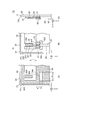
- FIG. 1 is a plan view of an antenna device according to a first embodiment of the present invention.
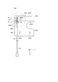
- FIG. 2 is an exploded plan view of the antenna device shown in FIG. 1. It is the figure which expanded and showed a part of antenna device enclosed with the broken-line circle
- FIG. 5 is an exploded plan view of the antenna device shown in FIG. 4.
- an antenna device (substrate antenna) 10 according to a first embodiment of the present invention will be described.
- the X-axis direction is the front-rear direction (depth direction)
- the Y-axis direction is the left-right direction (width direction, lateral direction)
- the Z-axis direction is the up-down direction (height direction).
- the illustrated antenna device 10 is for transmitting and receiving radio waves in a predetermined frequency band.
- the predetermined frequency band is a frequency in the 2.4 GHz band used in IEEE 802.11b / g.
- the illustrated antenna device 10 includes a coaxial cable 20 and an antenna element 30.
- the coaxial cable 20 is a coaxial electric signal transmission medium including a cylindrical outer conductor 21 and a central conductor 22 at the center thereof.
- the outer conductor 21 and the center conductor 22 are insulated by a cylindrical insulator 23.
- the outer conductor 21 is covered with a sheath 24.
- the outer conductor 21 is also called a ground wire or an outer conductor, and is made of a net-like conductor as shown in FIG.
- the center conductor 22 is also called a core wire or an inner conductor.
- the coaxial cable 20 has a diameter of 0.8 mm.
- the outer diameter of the outer conductor 21 is 0.6 mm.
- the coaxial cable 20 extends in the front-rear direction (X-axis direction).
- the front end portion of the coaxial cable 20 is cut as shown in FIG. 2, and the center conductor 22, the insulator 23, and the outer conductor 21 are exposed.
- the antenna element 30 has a flat printed wiring board 31 having a main surface (surface, upper surface) 31u.
- the printed wiring board 31 has a rectangular plate shape having a length (vertical) B and a width (horizontal) W. In the illustrated example, the length (length) B is 24.7 mm, and the width (width) W is 22.8 mm. In the illustrated example, the printed wiring board 31 has an opening 31a at the center of the right cotton.
- the printed wiring board 31 is provided with a pair of mounting holes 31b for mounting the antenna device 10 to a housing (not shown).
- the antenna element 30 has an antenna pattern portion 32 and a ground pattern portion 34 formed on the main surface 31 u of the printed wiring board 31.
- the antenna element 30 (the antenna pattern portion 32 and the ground pattern portion 34) is covered with a resist film (not shown) formed on the main surface 31u of the printed wiring board 31.
- the ground pattern portion 34 is integrally formed with the antenna pattern portion 32.
- the antenna pattern portion 32 and the ground pattern portion 34 are made of copper foil.
- the antenna pattern unit 32 is configured by an inverted F antenna.
- the inverted F antenna 32 includes an L-shaped L-shaped portion 322 and a power feeding portion 324 protruding from the L-shaped portion 322.
- the L-shaped portion 322 has a long side extending in the lateral direction (Y-axis direction) and a short side extending in the front-rear direction (X-axis direction).
- the antenna pattern portion 32 and the ground pattern portion 34 are made of copper foil, but may be made of other conductive foil.
- the coaxial cable 20 is formed on the ground pattern portion 34 in a direction (front-rear direction X) orthogonal to the longitudinal direction (left-right direction Y) of the antenna pattern portion 32 and one side of the ground pattern portion 34 ( It extends in parallel along the left side.
- the central conductor 22 of the coaxial cable 20 is electrically connected by solder 51 to the power feeding part 324 of the antenna pattern part 32 exposed from the first deletion part 511 of the resist film. That is, the power feeding unit 324 functions as a first soldering part.
- the outer conductor 21 of the coaxial cable 20 is electrically connected by soldering 52 at the second soldering portion 344 of the ground pattern portion 34 exposed from the second deletion portion 522 of the resist film.
- the ground pattern portion 34 has a rectangular ground pattern opening 34 a that defines the position of the second soldering portion 344 in the vicinity of the second soldering portion 344. .
- FIG. 3 is an enlarged view of a part of the antenna device 10 surrounded by a broken-line circle in FIG. 3,
- (A) is an enlarged plan view of a main part showing a state before soldering, and
- (B) and (C) are an enlarged plan view of a main part and an enlarged main part showing a state after soldering, respectively. It is a side view.
- the ground pattern opening 34a is heated by a soldering iron (not shown). This is to prevent escape from the second soldering portion 344. Thereby, the temperature of the 2nd soldering part 344 can be made more than soldering temperature in a short time. As a result, the outer conductor 21 of the coaxial cable 20 can be easily soldered to the ground pattern portion 34.
- the inventor has confirmed that the electrical performance of the antenna device 10 is not affected by the presence or absence of the ground pattern opening 34a.
- the position of the second soldering portion 344 is defined as follows.
- the second soldering portion 344 is between the ground pattern opening 34a and the upper end side 341 of the ground pattern portion 34, that is, a range defined by the width B in FIG. In the range defined by the width C.
- the power feeding unit 324 and the ground pattern opening 34 a are provided to face each other via the second soldering portion 344. In other words, the second soldering portion 344 is sandwiched between the power feeding portion (first soldering portion) 324 and the ground pattern opening 34a.
- the length C in the left-right direction Y of the ground pattern opening 34a is 3.4 mm, and the width A in the front-rear direction X is 1 mm.
- the width B of the second soldering portion 344 has substantially the same length as the length of the exposed outer conductor 21 of the coaxial cable 20. In the illustrated example, the width B is 1.5 mm. The width B may be a dimension that ensures the strength for soldering the solder 52.
- the width A of the ground pattern opening 34a only needs to be a width necessary for heat insulation when the solder 52 is soldered.
- the dimension A is preferably as small as possible. Therefore, it is preferable that 0.2 mm ⁇ A ⁇ B.
- an orthogonal coordinate system (X, Y, Z) is adopted. 4 and 5, the X-axis direction is the front-rear direction (depth direction), the Y-axis direction is the left-right direction (width direction, lateral direction), and the Z-axis direction is the up-down direction (height direction). ).
- the illustrated antenna device 10A has the same configuration as the antenna device 10 shown in FIGS. 1 and 2 except that the configuration of the antenna elements is different from that shown in FIGS. Therefore, the reference numeral 30A is attached to the antenna element.
- Components having the same functions as those shown in FIGS. 1 and 2 are denoted by the same reference numerals, and only differences will be described in detail below for the sake of simplicity.
- the illustrated antenna device 10A is for transmitting and receiving radio waves in a predetermined frequency band.
- the predetermined frequency band is a frequency in the 2.4 GHz band used in IEEE 802.11b / g.
- the antenna element 30A is formed by pressing a flat metal plate having a main surface (surface, upper surface) 30Au.
- the metal plate is made of phosphor bronze that has not been plated.
- phosphor bronze is used as the material of the metal plate, but the material for the metal plate is not limited to this.
- the antenna element 30A has an antenna pattern portion 32A and a ground pattern portion 34A integrally formed with the antenna pattern portion 32A.
- the antenna pattern portion 32A is composed of an inverted F antenna.
- the inverted F antenna 32A has an L-shaped L-shaped portion 322A and a power feeding portion 324A protruding from the L-shaped portion 322A.
- the L-shaped portion 322A has a long side extending in the horizontal direction (Y-axis direction) and a short side extending in the front-rear direction (X-axis direction).
- the ground pattern portion 34A has a substantially rectangular shape, but has an opening 34Ab on the upper right side.
- the ground pattern portion 34A has a pair of mounting holes 34Ac for mounting the antenna device 10A to a housing (not shown).
- the coaxial cable 20 is arranged on the ground pattern portion 34A in a direction (front-rear direction X) orthogonal to the longitudinal direction (left-right direction Y) of the antenna pattern portion 32A and on one side ( It extends in parallel along the left side.
- the central conductor 22 of the coaxial cable 20 is electrically connected by soldering the solder 51 to the power feeding part 324A of the antenna pattern part 32A. That is, the power feeding unit 324A functions as a first soldering part.
- the outer conductor 21 of the coaxial cable 20 is electrically connected by soldering the solder 52 at the second soldering portion 344A of the ground pattern portion 34A.
- the ground pattern portion 34A has a rectangular ground pattern opening 34Aa that defines the second soldering portion 344A in the vicinity of the second soldering portion 344A.
- the second soldering portion 344A is sandwiched between the power feeding portion (first soldering portion) 324A and the ground pattern opening 34Aa.
- the heat of the soldering iron (not shown) is first generated. This is to prevent escape from the second soldering portion 344A. As a result, the temperature of the second soldering portion 344A can be raised to the soldering temperature or higher in a short time. As a result, the outer conductor 21 of the coaxial cable 20 can be easily soldered to the ground pattern portion 34A.
- the inventor has confirmed that the electrical performance of the antenna device 10A is not affected by the presence or absence of the ground pattern opening 34Aa.
- the width of the second soldering portion 344A has the same dimensions as the width of the second soldering portion 344 described with reference to FIG.
- the length and width of the ground pattern opening 34Aa have the same dimensions as the length and width of the ground pattern opening 34a described with reference to FIG.
- the present invention has been described above with reference to preferred embodiments, it is needless to say that the present invention is not limited to the above-described embodiments.
- the antenna pattern portion is not limited to the inverted F antenna of the above-described embodiment, and it is needless to say that antenna pattern portions having various shapes may be employed.
- the ground pattern opening has a rectangular shape.
- the present invention is not limited to this, and the ground pattern opening may have an arbitrary shape.
- An antenna device capable of easily soldering the outer conductor of the coaxial cable to the ground pattern portion can be provided.
- Antenna device (substrate antenna) 10A antenna device (sheet metal antenna) 20 Coaxial cable (feed line) 21 Outer conductor 22 Central conductor 23 Insulator 24 Sheath 30, 30A Antenna element 30Au Main surface (upper surface, front surface) 31 Printed wiring board 31u Main surface (upper surface, front surface) 32, 32A Antenna pattern part 322, 322A L-shaped part 324, 324A Power feeding part (first soldering part) 34, 34A Ground pattern portion 341 Upper end side 344, 344A Second soldering portion 34a, 34Aa Ground pattern opening 51, 52 Solder 511, 522 Resist film deletion portion A Ground pattern opening width B Second soldering Part width C Length of ground pattern opening
Landscapes
- Engineering & Computer Science (AREA)
- Computer Networks & Wireless Communication (AREA)
- Waveguide Aerials (AREA)
- Details Of Aerials (AREA)
Abstract
同軸ケーブルの外部導体をグランドパターン部に容易に半田付けすることが可能なアンテナ装置を提供すること。 電波を送受信可能なアンテナ装置10は、中心導体22と外部導体21とを持つ同軸ケーブル20と、アンテナ素子30とを有する。アンテナ素子30は、アンテナパターン部32とグランド部34とを有する。中心導体22はアンテナパターン部32の第1の半田付け部分324に半田付けされ、外部導体21はグランドパターン部34の第2の半田付け部分344に半田52が半田付けされている。グランドパターン部34は、第2の半田付け部分344を画成する開口部34aを有する。第2の半田付け部分344は、第1の半田付け部分324と開口部34aとの間に配置されている。
Description
本発明は、アンテナ装置に関し、特に、無線LAN(Local Area Network)の周波数帯で使用されるアンテナ装置に関する。
この技術分野において周知のように、無線LANとは、電波や赤外線など、有線ケーブル以外の伝送路を利用したLANをいう。
無線LANの標準化については、米IEEE(米国電気電子技術者協会)の802.11委員会で策定されている。すなわち、このIEEE802.11委員会では、無線LANの標準の規格、仕様を策定している。
例えば、IEEE 802.11aは、IEEE 802.11委員会が策定した5GHz帯高速無線LAN・無線アクセスの規格である。通信速度(転送速度)は20M~50Mビット/秒程度である。MAC(媒体アクセス制御)としてはCSMA/CD(carrier sense multiple access with collision detection)が採用されている。物理層の変調方式はOFDM(直交周波数分割多重)である。
一方、IEEE 802.11bは、IEEE 802.11委員会が1999年9月に標準化した無線LANの仕様である。IEEE 802.11bでは、2.4GHz帯の周波数を使い、変調方式には直接拡散(DS)を使う。伝送速度(転送速度)は11Mビット/秒と5.5Mビット/秒とがある。
更に、IEEE 802.11gは、IEEE 802.11委員会が2003年6月に策定した、無線LANの標準規格の一つで、2.4GHz帯で約54Mビット/秒の通信を行う仕様である。変調方式にはOFDMが採用されている。したがって、IEEE802.11gは、IEEE 802.11bと同じ2.4GHz帯の周波数を利用し、IEEE 802.11bの約5倍にあたる54Mビット/秒の転送速度をサポートする。同じく54Mビット/秒の転送速度をサポートするIEEE 802.11aと異なり、IEEE 802.11gはIEEE 802.11bとの互換性もある。なお、54Mビット/秒という最高転送速度はIEEE 802.11aとまったく同じになっているが、2.4GHz帯は無線LAN以外の機器でも多数使用されている「混雑した」周波数帯となっているため、IEEE 802.11gでは実際の転送速度はIEEE 802.11aよりも遅くなるといわれている。
前述したように、IEEE 802.11bとIEEE 802.11gとでは使用周波数帯が同じ2.4GHz帯なので、ここでは、両方を合わせて、IEEE 802.11b/gと総称することにする。
このような無線LANの周波数帯で使用されるアンテナ装置は、従来から種々知られている。
例えば、特許文献1は、小型化及び実装が容易な平面偏波アンテナを開示している。特許文献1に開示された平面偏波アンテナは、平板絶縁基板と、この平板絶縁基板上に設けられる導電体部とを備える。導電体部は、給電点を有する逆Fアンテナ部と、グランド面部とを備える。同軸ケーブルの芯線(中心導体)は、逆Fアンテナ部の給電点に接続され、同軸ケーブルのアース線(外部導体)は、グランド面部に接続されている。
また、特許文献2は、安定した通信が確保でき、スペース効率に優れた平面アンテナを開示している。特許文献2に開示された平面アンテナは、絶縁性基材上にエレメント、グランド板および短絡部を配設し、絶縁性基材の他方の面に形成されたストリップラインを介し給電している。ストリップラインは開始点と終点とを持つ。ストリップラインの開始点は、絶縁性基材に設けられた一方のスルーホールを形成し、ストリップラインの終点は、絶縁性基材に設けられた別のスルーホールを形成している。給電用同軸ケーブルの内部導体はストリップラインの開始点に接続され、エレメントの給電点はストリップラインの終点に接続されている。尚、給電用同軸ケーブルの外部導体は、グランド板のアースポイントと接続されている。
上述した特許文献1及び2に開示されたアンテナ装置は、いずれも、基板上にアンテナパターンが形成されているので、「基板アンテナ」と呼ばれる。
一方、特許文献3は、広帯域および高利得のアンテナを開示している。特許文献3に開示されたアンテナは、少なくとも1つの折れ曲がり部を設けたアンテナエレメントと、このアンテナエレメントの一端が接続されるグランド部と、折れ曲がり部からこの折れ曲がり部の内角を分割する方向に形成した給電部と、この給電部に接続される給電線路とを有する。給電部には、給電線路である同軸ケーブルの内部導体が接続されている。同軸ケーブルの外部導体は、グランド部に接続されている。アンテナを製造する場合、例えばりん青銅等の平板を用いてプレス加工を行い、アンテナエレメントとグランド部およびアンテナエレメントの折れ曲がり部に給電部を設けた導体平板を形成する。このような導体平板を用いたアンテナは、「板金アンテナ」と呼ばれる。
また、特許文献4は、アンテナと通信ケーブルとをハンダ付け等により接続する際、送受信周波数のずれを防止することができ、接続作業性を向上させた、アンテナと通信ケーブルの接続構造を開示している。特許文献4において、アンテナは、金属部材からなるアンテナエレメントと、このアンテナエレメントの表面上の少なくとも一部に備えられた絶縁層とからなる。絶縁層に2つの窓穴が形成されている。これら窓穴を介して、アンテナエレメントと通信ケーブルの導体部分とが接続されている。アンテナエレメントは、放射導体部、接地導体部、短絡導体部、および給電路から構成されている。接地導体部は矩形をしている。通信ケーブルは、内部導体と外部導体とを有する。第1の窓穴を介して接地導体部と外部導体とがハンダを用いて接続され、第2の窓穴を介して給電路と内部導体とがハンダを用いて接続されている。通信ケーブルは、アンテナエレメントの長手方向と平行に延在している。
特許文献5は、小型、軽量で、しかも同調周波数帯域が広い多周波アンテナを開示している。特許文献5に開示された多周波アンテナは、X軸方向に延在するアンテナ素子と、このアンテナ素子と短絡ラインを介して導通接続されたグランド板と、アンテナ素子の長手方向と平行に延在し、かつ、アンテナ素子とグランド板との間に配置された同軸ケーブルとを備える。アンテナ素子の給電点から給電ラインが延在している。グランド板は、アンテナ素子側へ突出する突出片を持つ。同軸ケーブルの中心導体は給電ラインに接続され、同軸ケーブルの外部導体は突出片に接続されている。
上述したような平面アンテナにおいては、同軸ケーブルの外部導体をグランド板(グランドパターン部)に半田付けで接続する必要がある。そのような半田付けは、以下のようにして行われる。半田ごてを使用してグランド板(グランドパターン部)の特定の箇所(すなわち、半田付けが為される箇所)に熱を加えて、当該特定の箇所の温度をはんだ付け温度以上に上昇させ、これにより半田を融かして、同軸ケーブルの外部導体とグランド板(グランドパターン部)とを接続する。すなわち、半田付けが為される箇所(特定の箇所)を、ハンダ付け温度以上に加熱する必要がある。
上述した特許文献1~5では、それぞれ、次に述べるような問題がある。
特許文献1に開示された平面偏波アンテナでは、グランド面部が矩形をしているので、半田ごての熱が上記特定の箇所からグランド面部の周囲へ逃げて拡散してしまう。その結果、上記特定の箇所の温度を、半田付け温度以上にできなかったり、半田付け温度以上にするのに時間がかかったりしてしまう。すなわち、半田付けが困難であるという問題がある。
特許文献2に開示された平面アンテナにおいても、グランド板が矩形をしているので、半田ごての熱がアースポイント(特定の箇所)からグランド板の周囲へ拡散してしまう。その結果、上記アースポイント(特定の箇所)の温度を、半田付け温度以上にできなかったり、半田付け温度以上にするのに時間がかかったりしてしまう。すなわち、半田付けが困難であるという問題がある。
特許文献3に開示されたアンテナでも、グランド部が矩形をしているので、半田ごての熱が上記特定の箇所からグランド部の周囲へ逃げて拡散してしまう。その結果、上記特定の箇所の温度を、半田付け温度以上にできなかったり、半田付け温度以上にするのに時間がかかったりしてしまう。すなわち、半田付けが困難であるという問題がある。
特許文献4に開示されたアンテナでは、絶縁層に穿設された第1の窓穴を介して、アンテナエレメントの接地導体部と通信ケーブルの外部導体とがハンダを用いて接続されている。このような構成では、半田ごての熱を接地導体部へ伝達させることが困難になる。その結果、半田付けが困難であるという問題がある。
特許文献5に開示された多周波アンテナでは、同軸ケーブルの外部導体は、グランド板の突出片に接続されている。この突出片は非常に小さいので、グランド板から剥がれてしまう恐れがある。このように、剥離強度が弱いので、アンテナパターンに歪みが発生する恐れがある。
したがって、本発明の課題は、同軸ケーブルの外部導体をグランドパターン部に容易に半田付けすることが可能なアンテナ装置を提供することにある。
本発明によれば、電波を送受信可能なアンテナ装置(10;10A)であって、中心導体(22)と外部導体(21)とを持つ同軸ケーブル(20)と、アンテナ素子(30;30A)とを有するアンテナ装置(10;10A)に於いて、前記アンテナ素子(30;30A)は、アンテナパターン部(32;32A)とグランドパターン部(34;34A)とを有し、前記同軸ケーブル(20)の中心導体(22)は前記アンテナパターン部(32;32A)の第1の半田付け部分(324;324A)に半田付け(51)されて電気的に接続され、前記同軸ケーブル(20)の外部導体(21)は前記グランドパターン部(34;34A)の第2の半田付け部分(344;344A)に半田(52)付けされて電気的に接続され、前記グランドパターン部(34;34A)は、第2の半田付け部分(344;344A)を画成する開口部(34a;34Aa)を有し、前記第2の半田付け部分(344;344A)は、前記第1の半田付け部分(324;324A)と前記開口部(34a;34Aa)との間に配置されていることを特徴とする、アンテナ装置(10;10A)が得られる。
上記アンテナ装置(10;10A)において、前記同軸ケーブル(20)は、前記グランドパターン部(32;32A)上で、前記アンテナパターン部(32;32A)の延伸方向(Y)と直交する方向(X)で、かつ前記グランドパターン部(34;34A)の一辺に平行に延在するものでよい。前記所定の周波数帯は、例えば、2.4GHz帯の周波数であってよい。前記アンテナパターン部(32;32A)は、例えば、逆Fアンテナから構成されてよい。この場合、前記第1の半田付け部分としての前記逆Fアンテナの給電部(324;324A)に、前記同軸ケーブル(20)の前記中心導体(22)が接続される。
本発明の第1の態様による上記アンテナ装置(10)によれば、前記アンテナパターン部(32)と前記グランドパターン部(34)とは、前記基板(31)の主面(31u)上に形成された導体箔から構成されている。前記導体箔は、例えば、銅箔から成る。
本発明の第2の態様による上記アンテナ装置(10A)によれば、前記アンテナ素子(30A)は金属板から構成されている。前記金属板は、りん青銅から構成されることが好ましい。
上記アンテナ装置(10;10A)において、前記グランドパターン開口部(34a;34Aa)は、前記同軸ケーブル(20)の軸方向(X)と直交する方向(Y)に長い矩形をしていることが好ましい。前記第2の半田付け部分(344;344A)の幅(B)は、前記外部導体(21)の露出した部分の長さに等しいことが望ましい。前記グランドパターン開口部(34a;34Aa)の幅(A)は、前記第2の半田付け部分(344;344A)の幅(B)より小さく0.2mm以上の範囲にあることが好ましい。前記グランドパターン開口部(34a;34Aa)の長さは、3.4mm以上5.4mm以下の範囲にあることが好ましい。
尚、上記括弧内の符号は、本発明の理解を容易にするために付したものであり、一例にすぎず、これらに限定されないのは勿論である。
本発明に係るアンテナ装置では、グランドパターン部に、当該第2の半田付け部分を画成する開口部を形成したので、半田付け時に、第2の半田付け部分から熱が逃げるのを阻止することができる。その結果、同軸ケーブルの外部導体をグランドパターン部に容易に半田付けすることが可能となる。
以下、図面を参照して、本発明の実施の形態について詳細に説明する。
図1および図2を参照して、本発明の第1の実施の形態に係るアンテナ装置(基板アンテナ)10について説明する。
図1および図2では、直交座標系(X,Y,Z)を採用している。図1および図2に図示した状態では、X軸方向は前後方向(奥行き方向)であり、Y軸方向は左右方向(幅方向、横方向)であり、Z軸方向は上下方向(高さ方向)である。
図示のアンテナ装置10は、所定の周波数帯の電波を送受信するためのものである。図示の例では、所定の周波数帯は、IEEE 802.11b/gで使用される2.4GHz帯の周波数である。
図示のアンテナ装置10は、同軸ケーブル20とアンテナ素子30とを有する。
図2に示されるように、同軸ケーブル20は、円筒状の外部導体21と、その中央にある中心導体22とからなる同軸形状の電気信号伝送媒体である。外部導体21と中心導体22との間は円筒状の絶縁体23で絶縁されている。また、外部導体21はシース24で覆われている。外部導体21は、アース線や外導体とも呼ばれ、図2に示されるように、網状の導線から成る。中心導体22は、芯線や内導体とも呼ばれる。
図示の例では、同軸ケーブル20は0.8mmの直径を有する。また、外部導体21の外径は、0.6mmである。
図1に示されるように、同軸ケーブル20は、前後方向(X軸方向)に延在している。同軸ケーブル20の先端部は、図2に示されるようにカットされ、中心導体22、絶縁体23、および外部導体21が露出している。
アンテナ素子30は、主面(表面、上面)31uを持つ平板状のプリント配線基板31を有する。プリント配線基板31は、長さ(縦)B、幅(横)Wを持つ矩形板の形状をしている。図示の例では、長さ(縦)Bが24.7mm、幅(横)Wが22.8mmである。尚、図示の例では、プリント配線基板31は、その右綿中央部に開口31aを持つ。また、プリント配線基板31には、当該アンテナ装置10を筐体(図示せず)に取り付けるための一対の取付け用穴31bが穿設されている。
アンテナ素子30は、プリント配線基板31の主面31u上に形成された、アンテナパターン部32とグランドパターン部34とを有する。尚、アンテナ素子30(アンテナパターン部32およびグランドパターン部34)は、プリント配線基板31の主面31u上に形成されたレジスト膜(図示せず)によって覆われている。グランドパターン部34は、アンテナパターン部32に一体形成されている。アンテナパターン部32とグランドパターン部34とは、銅箔から成る。図示の例では、アンテナパターン部32は逆Fアンテナから構成されている。逆Fアンテナ32は、L字形状のL型部322と、このL型部322から突出する給電部324とを有する。L型部322は、横方向(Y軸方向)に延びる長辺と、前後方向(X軸方向)に延びる短辺とを有する。
尚、図示の例では、アンテナパターン部32とグランドパターン部34とは銅箔から構成されているが、他の導体箔から構成されても良い。
図1に示されるように、同軸ケーブル20は、グランドパターン部34上で、アンテナパターン部32の長手方向(左右方向Y)と直交する方向(前後方向X)でかつグランドパターン部34の一辺(左辺)に沿って平行に延在している。
同軸ケーブル20の中心導体22は、レジスト膜の第1の削除部511から露出したアンテナパターン部32の給電部324に半田51付けにより電気的に接続されている。すなわち、給電部324は、第1の半田付け部分として働く。
一方、同軸ケーブル20の外部導体21は、レジスト膜の第2の削除部522から露出したグランドパターン部34の第2の半田付け部分344で半田52付けにより電気的に接続されている。
本発明の第1の実施の形態では、グランドパターン部34は、第2の半田付け部分344の近傍に、当該第2の半田付け部分344の位置を規定する矩形のグランドパターン開口部34aを有する。
図3は、図1の破線円で囲んだアンテナ装置10の一部分を、拡大して示した図である。図3において、(A)は半田付け前の状態を示す要部拡大平面図であり、(B)および(C)は、それぞれ、半田付け後の状態を示す要部拡大平面図および要部拡大側面図である。
グランドパターン開口部34aは、同軸ケーブル20の外部導体21を、グランドパターン部34の第2の半田付け部分344で半田52を半田付けする際に、半田ごて(図示せず)の熱が第2の半田付け部分344から逃げるのを防止するためのものである。これにより、第2の半田付け部分344の温度を短時間で半田付け温度以上にすることができる。その結果、同軸ケーブル20の外部導体21をグランドパターン部34に容易に半田付けすることが可能となる。
尚、本発明者は、グランドパターン開口部34aの有無により、アンテナ装置10の電気性能に影響が無いことを確認している。
第2の半田付け部分344の位置は以下のように規定されている。
第2の半田付け部分344は、グランドパターン開口部34aとグランドパターン部34の上端辺341との間、つまり図3(A)において幅Bで規定される範囲であって、図3(A)において幅Cで規定される範囲に配置される。また、給電部324とグランドパターン開口部34aとは、第2の半田付け部分344を介して対向して設けられている。換言すれば、第2の半田付け部分344は、給電部(第1の半田付け部分)324とグランドパターン開口部34aとの間に挟まれている。
図示の例では、グランドパターン開口部34aの左右方向Yの長さCは3.4mmであり、前後方向Xの幅Aは1mmである。
また、第2の半田付け部分344の幅Bは、同軸ケーブル20の露出した外部導体21の長さと実質的に同一の長さを有する。図示の例では、幅Bは1.5mmである。この幅Bは、半田52を半田付けする強度を確保する程度の寸法であれば良い。
一方、グランドパターン開口部34aの幅Aは、半田52を半田付けする時の熱遮断に必要な幅があれば良い。また、アンテナ特性を良くするために、この寸法Aは極力小さいことが好ましい。したがって、0.2mm≦A<Bであることが好ましい。
グランドパターン開口部34aの長さCに関しては、その長さCを右方向に長くすればする程、半田52を半田付けする時間を短くすることが可能となる。それは、第2の半田付け部分344から熱が逃げるのを抑えることができるからである。逆に、長さCを延長し過ぎると、電気的特性に悪影響を与えてしまう。したがって、3.4mm≦C≦5.4mmの範囲であることが好ましい。
図4および図5を参照して、本発明の第2の実施の形態に係るアンテナ装置10Aについて説明する。
図4および図5では、直交座標系(X,Y,Z)を採用している。図4および図5に図示した状態では、X軸方向は前後方向(奥行き方向)であり、Y軸方向は左右方向(幅方向、横方向)であり、Z軸方向は上下方向(高さ方向)である。
図示のアンテナ装置10Aは、アンテナ素子の構成が、図1および図2に示したものと相違する点を除いて、図1および図2に示したアンテナ装置10と同様の構成を有する。従って、アンテナ素子に30Aの参照符号を付してある。図1および図2に示された構成要素と同様の機能の有するものには同一の参照符号を付し、以下では、説明を簡略化するために相違点についてのみ詳細に説明する。
図示のアンテナ装置10Aは、所定の周波数帯の電波を送受信するためのものである。図示の例では、所定の周波数帯は、IEEE 802.11b/gで使用される2.4GHz帯の周波数である。
アンテナ素子30Aは、主面(表面、上面)30Auを持つ平板状の金属板をプレス加工することによって形成される。図示の例では、金属板は、メッキ処理が施されていない、りん青銅から成る。
尚、図示の例では、金属板の材料としてりん青銅を使用しているが、金属板の材用はこれに限定されない。
アンテナ素子30Aは、アンテナパターン部32Aと、このアンテナパターン部32Aに一体形成されたグランドパターン部34Aとを有する。図示の例では、アンテナパターン部32Aは逆Fアンテナから構成されている。逆Fアンテナ32Aは、L字形状のL型部322Aと、このL型部322Aから突出する給電部324Aとを有する。L型部322Aは、横方向(Y軸方向)に延びる長辺と、前後方向(X軸方向)に延びる短辺とを有する。グランドパターン部34Aは、実質的に矩形形状をしているが、右側上部に開口34Abを持つ。また、グランドパターン部34Aには、当該アンテナ装置10Aを筐体(図示せず)に取り付けるための一対の取付け用穴34Acが穿設されている。
図4に示されるように、同軸ケーブル20は、グランドパターン部34A上で、アンテナパターン部32Aの長手方向(左右方向Y)と直交する方向(前後方向X)でかつグランドパターン部34Aの一辺(左辺)に沿って平行に延在している。
同軸ケーブル20の中心導体22は、アンテナパターン部32Aの給電部324Aに半田51を半田付けすることにより電気的に接続されている。すなわち、給電部324Aは、第1の半田付け部分として働く。
一方、同軸ケーブル20の外部導体21は、グランドパターン部34Aの第2の半田付け部分344Aで半田52を半田付けすることにより電気的に接続されている。
本発明の第2の実施の形態では、グランドパターン部34Aは、第2の半田付け部分344Aの近傍に、当該第2の半田付け部分344Aを規定する矩形のグランドパターン開口部34Aaを有する。第2の半田付け部分344Aは、給電部(第1の半田付け部分)324Aとグランドパターン開口部34Aaとの間に挟まれている。
グランドパターン開口部34Aaは、同軸ケーブル20の外部導体21を、グランドパターン部34Aの第2の半田付け部分344Aで半田52を半田付けする際に、半田ごて(図示せず)の熱が第2の半田付け部分344Aから逃げるのを防止するためのものである。これにより、第2の半田付け部分344Aの温度を短時間で半田付け温度以上に上昇させることができる。その結果、同軸ケーブル20の外部導体21をグランドパターン部34Aに容易に半田付けすることが可能となる。
尚、本発明者は、グランドパターン開口部34Aaの有無により、アンテナ装置10Aの電気性能に影響が無いことを確認している。
第2の半田付け部分344Aの幅は、図3を参照して説明した、第2の半田付け部分344の幅と同様の寸法を有する。また、グランドパターン開口部34Aaの長さおよび幅も、図3を参照して説明した、グランドパターン開口部34aの長さ及び幅と同様の寸法を有する。
以上、本発明について好ましい実施の形態によって説明してきたが、本発明は上述した実施の形態に限定しないのは勿論である。例えば、アンテナパターン部は、上述した実施の形態の逆Fアンテナに限定されず、種々の形状のアンテナパターン部を採用してもよいのは勿論である。また、上述した実施の形態では、グランドパターン開口部は矩形をしているが、これに限定されず、グランドパターン開口部は任意の形状をしていて良い。
本発明を詳細にまた特定の実施態様を参照して説明してきたが、本発明の精神、範囲または意図の範囲を逸脱することなく様々な変更や修正を加えることができることは当業者にとって明らかである。
本発明は、2009年7月10日出願の日本特許出願(特願2009-163889)に基づくものであり、その内容はここに参照として取り込まれる。
本発明を詳細にまた特定の実施態様を参照して説明してきたが、本発明の精神、範囲または意図の範囲を逸脱することなく様々な変更や修正を加えることができることは当業者にとって明らかである。
本発明は、2009年7月10日出願の日本特許出願(特願2009-163889)に基づくものであり、その内容はここに参照として取り込まれる。
同軸ケーブルの外部導体をグランドパターン部に容易に半田付けすることが可能なアンテナ装置を提供することができる。
10 アンテナ装置(基板アンテナ)
10A アンテナ装置(板金アンテナ)
20 同軸ケーブル(給電線)
21 外部導体
22 中心導体
23 絶縁体
24 シース(外皮)
30、30A アンテナ素子
30Au 主面(上面、表面)
31 プリント配線基板
31u 主面(上面、表面)
32、32A アンテナパターン部
322、322A L型部
324、324A 給電部(第1の半田付け部分)
34、34A グランドパターン部
341 上端辺
344、344A 第2の半田付け部分
34a、34Aa グランドパターン開口部
51、52 半田
511、522 レジスト膜の削除部
A グランドパターン開口部の幅
B 第2の半田付け部分の幅
C グランドパターン開口部の長さ
10A アンテナ装置(板金アンテナ)
20 同軸ケーブル(給電線)
21 外部導体
22 中心導体
23 絶縁体
24 シース(外皮)
30、30A アンテナ素子
30Au 主面(上面、表面)
31 プリント配線基板
31u 主面(上面、表面)
32、32A アンテナパターン部
322、322A L型部
324、324A 給電部(第1の半田付け部分)
34、34A グランドパターン部
341 上端辺
344、344A 第2の半田付け部分
34a、34Aa グランドパターン開口部
51、52 半田
511、522 レジスト膜の削除部
A グランドパターン開口部の幅
B 第2の半田付け部分の幅
C グランドパターン開口部の長さ
Claims (14)
- 電波を送受信可能なアンテナ装置であって、
中心導体と外部導体とを持つ同軸ケーブルと、
アンテナパターン部とグランドパターン部とを有するアンテナ素子と、
を具備して成り、
前記中心導体は、前記アンテナパターン部の第1の半田付け部分に半田付けされて電気的に接続され、
前記外部導体は、前記グランドパターン部の第2の半田付け部分に半田付けされて電気的に接続され、
前記グランドパターン部は、当該第2の半田付け部分を画成する開口部を有し、前記第2の半田付け部分は、前記第1の半田付け部分と前記開口部との間に配置されていることを特徴とする、アンテナ装置。 - 前記同軸ケーブルは、前記グランドパターン部上で、前記アンテナパターン部の延伸方向と直交する方向で、かつ前記グランドパターン部の一辺に平行に延在する請求項1に記載のアンテナ装置。
- 前記電波の周波数帯が、2.4GHz帯の周波数である、請求項1又は2に記載のアンテナ装置。
- 前記アンテナパターン部は逆Fアンテナからなり、
前記逆Fアンテナの給電部は、前記第1の半田付け部分を含む、請求項1乃至3のいずれか1つに記載のアンテナ装置。 - 前記アンテナパターン部と前記グランドパターン部とは、基板の主面上に設けられている、請求項1乃至4のいずれか1つに記載のアンテナ装置。
- 前記アンテナパターン部と前記グランドパターン部とは、前記基板の主面上に設けられた導体箔から成る、請求項5に記載のアンテナ装置。
- 前記導体箔は銅箔から成る、請求項6に記載のアンテナ装置。
- 前記アンテナ素子は金属板から構成されている、請求項1乃至4のいずれか1つに記載のアンテナ装置。
- 前記金属板がりん青銅から成る、請求項8に記載のアンテナ装置。
- 前記開口部は、前記同軸ケーブルの軸方向と直交する方向に延伸した矩形形状を有する、請求項1乃至9のいずれか1つに記載のアンテナ装置。
- 前記第2の半田付け部分の幅は、前記外部導体の露出した部分の長さに等しい、請求項10に記載のアンテナ装置。
- 前記開口部の幅は、前記第2の半田付け部分の幅より小さく0.2mm以上である、請求項10又は11に記載のアンテナ装置。
- 前記グランドパターン開口部の長さは、3.4mm以上5.4mm以下である、請求項10乃至12のいずれか1つに記載のアンテナ装置。
- アンテナ素子であって、
第1部分を有するアンテナパターン部と、
第2部分を有するグランドパターン部と、
を具備して成り、
前記グランドパターン部は、前記第2部分の一部によって画成される開口を有して形成され、
前記第2部分は、前記第1部分と前記開口との間に配置される。
Priority Applications (1)
| Application Number | Priority Date | Filing Date | Title |
|---|---|---|---|
| US13/382,622 US8872726B2 (en) | 2009-07-10 | 2010-05-07 | Antenna device |
Applications Claiming Priority (2)
| Application Number | Priority Date | Filing Date | Title |
|---|---|---|---|
| JP2009163889A JP5110326B2 (ja) | 2009-07-10 | 2009-07-10 | アンテナ装置 |
| JP2009-163889 | 2009-07-10 |
Publications (1)
| Publication Number | Publication Date |
|---|---|
| WO2011004649A1 true WO2011004649A1 (ja) | 2011-01-13 |
Family
ID=43429075
Family Applications (1)
| Application Number | Title | Priority Date | Filing Date |
|---|---|---|---|
| PCT/JP2010/057785 Ceased WO2011004649A1 (ja) | 2009-07-10 | 2010-05-07 | アンテナ装置 |
Country Status (3)
| Country | Link |
|---|---|
| US (1) | US8872726B2 (ja) |
| JP (1) | JP5110326B2 (ja) |
| WO (1) | WO2011004649A1 (ja) |
Cited By (1)
| Publication number | Priority date | Publication date | Assignee | Title |
|---|---|---|---|---|
| TWI774181B (zh) * | 2020-03-11 | 2022-08-11 | 日商日本航空電子工業股份有限公司 | 天線組件以及電子裝置 |
Families Citing this family (9)
| Publication number | Priority date | Publication date | Assignee | Title |
|---|---|---|---|---|
| US9585810B2 (en) | 2010-10-14 | 2017-03-07 | Fresenius Medical Care Holdings, Inc. | Systems and methods for delivery of peritoneal dialysis (PD) solutions with integrated inter-chamber diffuser |
| JP5510836B2 (ja) * | 2011-03-28 | 2014-06-04 | 日立金属株式会社 | アンテナ及びそれを備えた無線装置 |
| JP2013138296A (ja) | 2011-12-28 | 2013-07-11 | Mitsumi Electric Co Ltd | アンテナ装置 |
| JP2013219746A (ja) * | 2012-03-15 | 2013-10-24 | Seiko Epson Corp | スリーブアンテナ及び無線通信装置 |
| USD681019S1 (en) * | 2012-09-07 | 2013-04-30 | Cheng Uei Precision Industry Co., Ltd. | Antenna |
| JP7453792B2 (ja) | 2020-01-16 | 2024-03-21 | 日本航空電子工業株式会社 | 固定具、固定方法、ケーブル組立体及び構造体 |
| JP7467127B2 (ja) | 2020-01-17 | 2024-04-15 | 日本航空電子工業株式会社 | ケーブル組立体及び構造体 |
| TWI770851B (zh) * | 2020-03-30 | 2022-07-11 | 仁寶電腦工業股份有限公司 | 天線裝置 |
| JP2022090818A (ja) * | 2020-12-08 | 2022-06-20 | ラピステクノロジー株式会社 | 無線モジュール |
Citations (4)
| Publication number | Priority date | Publication date | Assignee | Title |
|---|---|---|---|---|
| JPH0456157A (ja) * | 1990-06-21 | 1992-02-24 | Shinko Electric Ind Co Ltd | 半導体装置のリード取り付け構造 |
| JP2005277897A (ja) * | 2004-03-25 | 2005-10-06 | Hitachi Cable Ltd | 平板アンテナ及びその製造方法 |
| JP2007014021A (ja) * | 2002-12-06 | 2007-01-18 | Fujikura Ltd | アンテナ |
| JP2008187631A (ja) * | 2007-01-31 | 2008-08-14 | Casio Comput Co Ltd | 平面偏波アンテナ及び電子機器 |
Family Cites Families (12)
| Publication number | Priority date | Publication date | Assignee | Title |
|---|---|---|---|---|
| JPS60111501A (ja) * | 1983-11-21 | 1985-06-18 | Toyo Commun Equip Co Ltd | ル−プアンテナエレメント素材 |
| JPH0832344A (ja) * | 1994-07-18 | 1996-02-02 | Nippon Valqua Ind Ltd | 板状アンテナおよびその製造方法 |
| JPH088629A (ja) * | 1994-12-08 | 1996-01-12 | Nec Corp | 小型無線機の内蔵アンテナ |
| JP2004173143A (ja) | 2002-11-22 | 2004-06-17 | Kurabe Ind Co Ltd | アンテナと通信ケーブルの接続部構造 |
| JP4473553B2 (ja) | 2003-11-05 | 2010-06-02 | 峰光電子株式会社 | 多周波アンテナ、及びその構成方法 |
| US20050035919A1 (en) * | 2003-08-15 | 2005-02-17 | Fan Yang | Multi-band printed dipole antenna |
| JP4381775B2 (ja) | 2003-10-31 | 2009-12-09 | 日星電気株式会社 | 平面アンテナ |
| TWI304664B (en) * | 2004-06-30 | 2008-12-21 | Hon Hai Prec Ind Co Ltd | Antenna |
| US7612720B2 (en) * | 2005-04-25 | 2009-11-03 | Koninklijke Philips Electronics N.V. | Wireless link module comprising two antennas |
| JP2007159064A (ja) | 2005-12-08 | 2007-06-21 | Sony Corp | アンテナとそれを用いた無線装置および電子機器 |
| JP4613950B2 (ja) * | 2007-12-27 | 2011-01-19 | カシオ計算機株式会社 | 平面モノポールアンテナ及び電子機器 |
| JP2010278586A (ja) * | 2009-05-27 | 2010-12-09 | Casio Computer Co Ltd | マルチバンド平面アンテナ及び電子機器 |
-
2009
- 2009-07-10 JP JP2009163889A patent/JP5110326B2/ja not_active Expired - Fee Related
-
2010
- 2010-05-07 US US13/382,622 patent/US8872726B2/en active Active
- 2010-05-07 WO PCT/JP2010/057785 patent/WO2011004649A1/ja not_active Ceased
Patent Citations (4)
| Publication number | Priority date | Publication date | Assignee | Title |
|---|---|---|---|---|
| JPH0456157A (ja) * | 1990-06-21 | 1992-02-24 | Shinko Electric Ind Co Ltd | 半導体装置のリード取り付け構造 |
| JP2007014021A (ja) * | 2002-12-06 | 2007-01-18 | Fujikura Ltd | アンテナ |
| JP2005277897A (ja) * | 2004-03-25 | 2005-10-06 | Hitachi Cable Ltd | 平板アンテナ及びその製造方法 |
| JP2008187631A (ja) * | 2007-01-31 | 2008-08-14 | Casio Comput Co Ltd | 平面偏波アンテナ及び電子機器 |
Cited By (2)
| Publication number | Priority date | Publication date | Assignee | Title |
|---|---|---|---|---|
| TWI774181B (zh) * | 2020-03-11 | 2022-08-11 | 日商日本航空電子工業股份有限公司 | 天線組件以及電子裝置 |
| US11764465B2 (en) | 2020-03-11 | 2023-09-19 | Japan Aviation Electronics Industry, Limited | Antenna assembly and electronic equipment |
Also Published As
| Publication number | Publication date |
|---|---|
| US20120105303A1 (en) | 2012-05-03 |
| US8872726B2 (en) | 2014-10-28 |
| JP2011019178A (ja) | 2011-01-27 |
| JP5110326B2 (ja) | 2012-12-26 |
Similar Documents
| Publication | Publication Date | Title |
|---|---|---|
| JP5110326B2 (ja) | アンテナ装置 | |
| US8917216B2 (en) | Antenna device with U-shaped slit | |
| CN112751158B (zh) | 一种天线组件及通信设备 | |
| JP2017195589A (ja) | アンテナおよび当該アンテナを含むアンテナモジュール | |
| US7667653B2 (en) | Antenna unit comprising first and second antenna patterns | |
| JP4780352B2 (ja) | アンテナ装置 | |
| JP5213039B2 (ja) | 片面放射アンテナ | |
| TWM319527U (en) | Planar antenna | |
| CN203895598U (zh) | 高增益双频阵列天线 | |
| JP6059001B2 (ja) | アンテナ装置 | |
| CN103594782A (zh) | 电路板天线 | |
| JP2008078752A (ja) | アンテナ装置 | |
| US6853348B1 (en) | Dual band linear antenna array | |
| US11996620B2 (en) | Antenna device | |
| CN215266649U (zh) | 天线及电子设备 | |
| CN101682124A (zh) | 锥形缝隙天线 | |
| JP3807675B2 (ja) | アンテナ | |
| CN216015709U (zh) | 一种基于cpw结构的wifi6e板载终端天线 | |
| KR102721543B1 (ko) | 무선통신용 fpcb 케이블 | |
| JP4457850B2 (ja) | 基板搭載薄型アンテナ | |
| CN116190960B (zh) | 一种太赫兹频段低损耗高集成度的芯片波导转接结构 | |
| JP2014220739A (ja) | プリント基板ダイポールアンテナ | |
| JP2012049783A (ja) | L字型折り返しモノポールアンテナ装置 | |
| JP4935256B2 (ja) | アンテナ装置 | |
| CN119404376A (zh) | 用于通信设备的天线组件 |
Legal Events
| Date | Code | Title | Description |
|---|---|---|---|
| 121 | Ep: the epo has been informed by wipo that ep was designated in this application |
Ref document number: 10796960 Country of ref document: EP Kind code of ref document: A1 |
|
| WWE | Wipo information: entry into national phase |
Ref document number: 13382622 Country of ref document: US |
|
| NENP | Non-entry into the national phase |
Ref country code: DE |
|
| 122 | Ep: pct application non-entry in european phase |
Ref document number: 10796960 Country of ref document: EP Kind code of ref document: A1 |