WO2011001740A1 - 研磨装置、研磨方法、露光装置及びデバイスの製造方法 - Google Patents
研磨装置、研磨方法、露光装置及びデバイスの製造方法 Download PDFInfo
- Publication number
- WO2011001740A1 WO2011001740A1 PCT/JP2010/057813 JP2010057813W WO2011001740A1 WO 2011001740 A1 WO2011001740 A1 WO 2011001740A1 JP 2010057813 W JP2010057813 W JP 2010057813W WO 2011001740 A1 WO2011001740 A1 WO 2011001740A1
- Authority
- WO
- WIPO (PCT)
- Prior art keywords
- polishing
- optical
- optical member
- liquid
- substrate
- Prior art date
- Legal status (The legal status is an assumption and is not a legal conclusion. Google has not performed a legal analysis and makes no representation as to the accuracy of the status listed.)
- Ceased
Links
Images


Classifications
-
- H—ELECTRICITY
- H10—SEMICONDUCTOR DEVICES; ELECTRIC SOLID-STATE DEVICES NOT OTHERWISE PROVIDED FOR
- H10P—GENERIC PROCESSES OR APPARATUS FOR THE MANUFACTURE OR TREATMENT OF DEVICES COVERED BY CLASS H10
- H10P76/00—Manufacture or treatment of masks on semiconductor bodies, e.g. by lithography or photolithography
- H10P76/20—Manufacture or treatment of masks on semiconductor bodies, e.g. by lithography or photolithography of masks comprising organic materials
- H10P76/204—Manufacture or treatment of masks on semiconductor bodies, e.g. by lithography or photolithography of masks comprising organic materials of organic photoresist masks
- H10P76/2041—Photolithographic processes
-
- G—PHYSICS
- G03—PHOTOGRAPHY; CINEMATOGRAPHY; ANALOGOUS TECHNIQUES USING WAVES OTHER THAN OPTICAL WAVES; ELECTROGRAPHY; HOLOGRAPHY
- G03F—PHOTOMECHANICAL PRODUCTION OF TEXTURED OR PATTERNED SURFACES, e.g. FOR PRINTING, FOR PROCESSING OF SEMICONDUCTOR DEVICES; MATERIALS THEREFOR; ORIGINALS THEREFOR; APPARATUS SPECIALLY ADAPTED THEREFOR
- G03F7/00—Photomechanical, e.g. photolithographic, production of textured or patterned surfaces, e.g. printing surfaces; Materials therefor, e.g. comprising photoresists; Apparatus specially adapted therefor
- G03F7/70—Microphotolithographic exposure; Apparatus therefor
- G03F7/70216—Mask projection systems
- G03F7/70341—Details of immersion lithography aspects, e.g. exposure media or control of immersion liquid supply
-
- G—PHYSICS
- G03—PHOTOGRAPHY; CINEMATOGRAPHY; ANALOGOUS TECHNIQUES USING WAVES OTHER THAN OPTICAL WAVES; ELECTROGRAPHY; HOLOGRAPHY
- G03B—APPARATUS OR ARRANGEMENTS FOR TAKING PHOTOGRAPHS OR FOR PROJECTING OR VIEWING THEM; APPARATUS OR ARRANGEMENTS EMPLOYING ANALOGOUS TECHNIQUES USING WAVES OTHER THAN OPTICAL WAVES; ACCESSORIES THEREFOR
- G03B27/00—Photographic printing apparatus
- G03B27/32—Projection printing apparatus, e.g. enlarger, copying camera
- G03B27/52—Details
Definitions
- the present invention relates to an exposure apparatus including an optical member such as a lens, and a device manufacturing method using the exposure apparatus.
- the present invention also relates to a polishing apparatus and a polishing method for polishing an optical member such as a lens.
- an exposure apparatus for forming a pattern (circuit pattern or the like) on a substrate such as a wafer or a glass plate coated with a photosensitive material is used.
- a projection optical system mounted on such an exposure apparatus includes a lens barrel and a plurality of optical members (such as lenses) accommodated in the lens barrel. These optical members are respectively supported by the lens barrel via optical member holding devices capable of displacing the optical member with respect to the lens barrel.
- the aberration (also referred to as wavefront aberration) of the projection optical system is adjusted by driving the optical member holding devices and adjusting the positions of the optical members.
- a pattern having an appropriate size and shape is formed on the substrate disposed on the image plane side of the projection optical system.
- Patent Documents 1 and 2 disclose a technique for removing foreign matters such as dirt attached to an optical member.
- the aberration of the projection optical system may change with time. Therefore, in the exposure apparatus, generally, the aberration of the projection optical system is adjusted regularly or irregularly.
- the only method for adjusting the aberration of the projection optical system in the conventional exposure apparatus is to displace each optical member. For this reason, there is a limit in adjusting the aberration of the projection optical system.
- the projection optical system is provided with a configuration for taking out some of the optical members outside the lens barrel, polishing the optical members taken out of the lens barrel, and removing the polished optical members.
- a method of re-installing in the lens barrel is conceivable (see Patent Document 3).
- this method has a problem that the optical member needs to be taken in and out inside and outside the lens barrel, and the operation becomes very complicated.
- the present invention has been made in view of such circumstances, and an object thereof is to provide a polishing apparatus, a polishing method, an exposure apparatus, and a device manufacturing method capable of easily adjusting aberrations of an optical system.
- An exposure apparatus illuminates a predetermined pattern with light (EL) and irradiates a substrate (W) coated with a photosensitive material with light (EL) via the predetermined pattern.
- An exposure apparatus (11), an optical member (18, 19, 20, 21, 22, 23, 27) disposed in the optical path of the light (EL) and the optical member (18, 19, 20, 21, 22, 23, 27) with an optical system (12, 14) having a support member (17) supporting the optical member (18, 19, 20, 21, 22, 23, 27) and a polishing device (37, 37 A, 65, 67, 76, 80) for changing the shape of the optical member (18, 19, 20, 21, 22, 23, 27), It is a summary to provide.
- the shape of the optical member (18, 19, 20, 21, 22, 23, 27) supported by the support member (17) is changed by the polishing device (37, 37A, 65).
- the aberration of the optical system (12, 14) is adjusted. Therefore, the optical member (18, 19, 20, 21, 22, 23, 27) is taken out from the optical system (12, 14), and the shape of the optical member (18, 19, 20, 21, 22, 23, 27) is obtained.
- the optical system (12, 14) can be saved by the trouble of taking out the optical member (18, 19, 20, 21, 22, 23, 27) from the optical system (12, 14). The adjustment of the adjustment is easy.
- a polishing apparatus illuminates a predetermined pattern with light (EL), and applies a substrate (W) coated with a photosensitive material with light (EL) through the predetermined pattern.
- the optical members (18, 19, 20, 21, 22, 23, 27) being supported by the support member (17) are polished, and the optical members (18, 19, 20, 21) are polished. , 22, 23, 27) To.
- the polishing method is a substrate (W) in which a predetermined pattern is illuminated with light (EL) and a photosensitive material is applied with light (EL) through the predetermined pattern.
- the optical member (18, 19, 20, 21, 22, 23, 27) and the optical member (18, 19, 20, 21, 27) disposed in the optical path of the light (EL)
- the optical members (18, 19, 20, 21, 22, 23, 27) of the exposure apparatus (11) including an optical system (12, 14) having a support member (17) for supporting the members 22, 23, 27).
- a polishing method for polishing wherein the optical member (18, 19, 20, 21, 22, 23, 27) supported by the support member (17) is polished, and the optical member (18, 19) is polished. , 20, 21, 22, 23, 27) It is the gist of.
- the aberration of the optical system can be easily adjusted.
- FIG. 1 is a schematic block diagram that shows an exposure apparatus in the present embodiment. Sectional drawing which shows typically the principal part of exposure apparatus.
- (A) and (b) are schematic diagrams showing how the peripheral edge of the exit side surface of the image side optical member is polished.
- (A) (b) is a schematic diagram which shows the liquid supply apparatus of another embodiment. The schematic diagram which shows the wafer stage of another embodiment. The schematic diagram which shows the grinding
- the direction parallel to the optical axis of the projection optical system is the Z-axis direction
- the scanning direction of the reticle R and wafer W during scanning exposure in a plane perpendicular to the Z-axis direction is the Y-axis direction
- the non-scanning direction orthogonal to the scanning direction will be described as the X-axis direction.
- the rotation directions around the X, Y, and Z axes are also referred to as the ⁇ x direction, the ⁇ y direction, and the ⁇ z direction.
- an exposure apparatus 11 uses exposure light EL emitted from a light source device (not shown) to illuminate a reticle R as a mask on which a predetermined circuit pattern is formed. It is an apparatus for projecting an image of a circuit pattern to be formed on a wafer W coated with a photosensitive material such as a resist.
- Such an exposure apparatus 11 irradiates the wafer W with the illumination light EL 12 that illuminates the reticle R with the exposure light EL from the light source device, the reticle stage 13 that holds the reticle R, and the exposure light EL that passes through the reticle R. And a wafer stage 15 that holds the wafer W.
- a light source that outputs ArF excimer laser light (wavelength 193 nm) as exposure light EL is used.
- the illumination optical system 12 includes an optical integrator (not shown) such as a fly-eye lens and a rod lens, various lens systems such as a relay lens and a condenser lens, and an aperture stop (not shown). Then, exposure light EL emitted from a light source device (not shown) passes through the illumination optical system 12, so that the reticle R has a uniform light intensity distribution (also referred to as light luminance distribution) and has an X axis. A substantially rectangular illumination region extending in a direction (a direction orthogonal to the paper surface in FIG. 1) is formed.
- the reticle stage 13 is arranged between the illumination optical system 12 and the projection optical system 14 so that the mounting surface 16 of the reticle R is substantially orthogonal to the optical path. That is, the reticle stage 13 is arranged on the object plane side (+ Z direction side, upper side in FIG. 1) of the projection optical system 14.
- the reticle stage 13 is provided with a holding unit (not shown) for holding the reticle R (for example, a vacuum chuck (not shown) for vacuum-sucking the reticle R).
- a holding unit for holding the reticle R
- Such a reticle stage 13 can be moved in the Y-axis direction (left-right direction in FIG. 1) by driving a reticle stage driving unit (not shown).
- the reticle stage drive unit moves the reticle R held by the holding unit with a predetermined stroke in the Y-axis direction.
- the reticle stage drive unit can move the reticle R in the X-axis direction and the ⁇ z direction as well.
- the projection optical system 14 is an optical system that reduces an image of a circuit pattern formed by illuminating the reticle R with exposure light EL to a predetermined reduction magnification (for example, 1/4), and has a substantially cylindrical shape.
- a lens barrel 17 is provided. The inside of the lens barrel 17 is filled with a purge gas such as nitrogen gas.
- a plurality of optical members (lenses in the present embodiment) 18, 19, 20, 21, 22, 23 are shown in the Z-axis direction (vertical direction in FIG. 1). Are arranged along.
- These optical members 18 to 23 are respectively supported by the lens barrel 17 via the holding device 24.
- Each holding device 24 is configured to be capable of displacing the optical members 18 to 23 that it holds individually in a plurality of directions.
- the configuration of the holding device 24 is disclosed in, for example, US Pat. No. 6,930,842 and US Patent Publication No. 2007/0183064.
- an annular ring formed so as to surround the emission portion 23 a of the optical member 23 is provided at the end portion (the lower end portion in FIG. 1) of the lens barrel 17 on the ⁇ Z direction side.
- the fixing member 25 is fixed by a plurality of first bolts 26 (only two are shown in FIG. 2). That is, the fixing member 25 is formed so as to surround the optical path of the exposure light EL emitted from the optical member 23.
- An image surface side optical member 27 (also referred to as “front lens”) is provided, and the image surface side optical member 27 is attached to the lens barrel 17 via an annular lens holder 28 and a fixing member 25. It is supported.
- the image surface side optical member 27 has a substantially circular shape when viewed from the Z-axis direction, and is formed at the center portion thereof and through which the exposure light EL passes.
- a light passage portion 29 is provided.
- the exposure light passage portion 29 is formed such that its exit side surface (surface on the ⁇ Z direction side) 30 is parallel to the incident side surface (surface on the + Z direction side) 31.
- the image surface side optical member 27 has an annular flange portion 32 formed on the outer peripheral side of the exposure light passage portion 29, and the optical axis of the projection optical system 14 is provided at the periphery of the flange portion 32.
- a plurality of locked portions 33 (only two are shown in FIG.
- the lens holder 28 is formed so that the inner side in the radial direction is located at the same position in the radial direction as each of the locked portions 33 of the image surface side optical member 27.
- locking concave portions 34 that can accommodate the locked portions 33 are formed at positions corresponding to the locked portions 33.
- a plurality of lens holders 28 (only two are shown in FIG. 2) in a state where each locked portion 33 individually corresponding to each locking recess 34 is accommodated in each locking recess 34.
- the image surface side optical member 27 is supported by the lens barrel 17 so as not to move by being fixed to the fixing member 25 by the two bolts 35. At this time, the surface on the + Z direction side of each locked portion 33 is in contact with the fixing member 25, and both side surfaces in the circumferential direction of each locked portion 33 are in contact with the side wall of each locking recess 34. ing.
- the predetermined space 36 between the image surface side optical member 27 and the wafer W is filled with the first liquid such as pure water during the exposure process on the wafer W by the operation of the liquid supply device 37.
- the exposure apparatus 11 of the present embodiment is a so-called immersion type exposure apparatus.
- the specific configuration of the liquid supply device 37 will be described later.
- the wafer stage 15 is arranged on the image plane side of the projection optical system 14 so that the mounting surface on which the wafer W is mounted intersects the optical path of the exposure light EL.
- the wafer stage 15 includes a holding unit 38 for holding the wafer W (for example, a vacuum chuck (not shown) for vacuum-sucking the reticle R), a wafer holder (not shown) for holding the holding unit 38, and the wafer holder
- a Z leveling mechanism (not shown) that adjusts the position in the Z-axis direction and the tilt angles around the X-axis and the Y-axis is incorporated.
- Such a wafer stage 15 can be moved in the Y-axis direction by a wafer stage driving unit (not shown).
- the wafer stage drive unit moves the wafer W held by the holding unit 38 in the Y axis direction with a predetermined stroke.
- the wafer stage drive unit is configured to be able to move the wafer W held by the holding unit 38 in the X-axis direction and the Z-axis direction.
- the reticle R When a circuit pattern of the reticle R is formed on one shot area of the wafer W, the reticle R is moved in the Y-axis direction by driving the reticle stage driving unit while the illumination area is formed on the reticle R by the illumination optical system 12.
- the projection optical system 14 is moved with respect to the movement of the reticle R along the Y-axis direction by moving the wafer stage drive unit (for example, from the + Y direction side to the ⁇ Y direction side) for every predetermined stroke. It is moved in synchronization with the Y-axis direction (for example, from the ⁇ Y direction side to the + Y direction side) at a speed ratio corresponding to the reduction magnification.
- the liquid supply device 37 includes a first liquid supply unit 41 that is driven to supply a first liquid (for example, pure water) used during exposure processing or the like into a predetermined space 36, and an image plane side. And a second liquid supply unit 42 that is driven to supply a second liquid (for example, a liquid containing an abrasive) used when the optical member 27 is polished.
- the liquid supply device 37 includes a liquid recovery unit 43 that is driven to recover the liquid in the predetermined space 36 and a switching unit 46 to which supply pipes 44 and 45 extending from the liquid supply units 41 and 42 are connected. Is provided.
- the switching unit 46 includes a switching valve (not shown) having two input ports and one output port, and the type of liquid that allows supply to a liquid supply / recovery member 47 described later by driving the switching valve. Selected.
- the liquid supply device 37 is provided with an annular liquid supply / recovery member 47.
- the liquid supply / recovery member 47 is supported by an unillustrated support mechanism by the image plane side optical member 27, the lens holder 28, and the wafer. It is supported so as not to contact W or the like.
- the liquid supply / recovery member 47 is disposed on the ⁇ Z direction side of the flange portion 32 of the image surface side optical member 27 and so as to surround the exposure light passage portion 29 of the image surface side optical member 27. Yes. That is, the inner surface 47a of the liquid supply / recovery member 47 faces the side surface 29a of the exposure light passage portion 29 of the image surface side optical member 27, and the surface (upper surface in FIG. 2) 47b on the + Z direction side is the image surface.
- the side optical member 27 is disposed so as to face the surface 32 a on the ⁇ Z direction side of the flange portion 32. Further, the portion on the ⁇ Z direction side of the liquid supply / recovery member 47 is located on the ⁇ Z direction side with respect to the exit side surface 30 of the image surface side optical member 27.
- the fluororesin is applied to the inner surface 47a of the liquid supply / recovery member 47 and the surface 47b on the + Z direction side, the side surface 29a of the exposure light passage portion 29, and the surface 32a on the ⁇ Z direction side of the flange portion 32. Water repellent treatment such as coating is applied.
- the liquid supply / recovery member 47 is connected to the switching unit 46 via the connection pipe 48 and is connected to the liquid recovery part 43 via the recovery pipe 49.
- a liquid supply passage 50 communicating with the connection pipe 48 is formed, and a liquid recovery passage 51 communicating with the recovery pipe 49 is formed.
- a plurality of supply nozzles 52 are formed on the inner side surface 47a of the liquid supply / recovery member 47 so as to surround the exit side surface 30 of the image surface side optical member 27 and the optical path of the exposure light EL and are arranged at equal intervals along the circumferential direction.
- a communication path (not shown) for communicating each supply nozzle 52 and the liquid supply path 50 is formed.
- each supply nozzle 52 the liquid (first liquid or second liquid) supplied through the liquid supply passage 50 is ejected toward the peripheral portion 30 a of the ejection side surface 30 of the image surface side optical member 27. (See FIG. 3 (a)). Further, an annular recovery nozzle 53 formed so as to surround the optical path of the exposure light EL is formed on the surface side of the liquid supply / recovery member 47 on the ⁇ Z direction side. It communicates with the passage 51.
- the recovery nozzle 53 is provided with a porous member 54 in which a large number of holes are formed.
- the liquid supply device 37 of the present embodiment is provided with a control device 55.
- the control device 55 includes a digital computer (not shown) constructed from a CPU, a ROM, a RAM, and the like, and a driver circuit (not shown) for driving the liquid supply units 41 and 42, the liquid recovery unit 43, and the switching unit 46. ing.
- the control device 55 controls the first liquid supply unit 41 and the switching unit 46 so that the first liquid is ejected from each supply nozzle 52 of the liquid supply / recovery member 47 during the exposure process.
- the control device 55 controls the first liquid supply unit 41 so that the first liquid is ejected from each supply nozzle 52 at the first flow velocity.
- the controller 55 recovers the liquid so that the liquid (that is, the first liquid) in the predetermined space 36 is recovered via the recovery nozzle 53 of the liquid supply recovery member 47 when the wafer W is subjected to exposure processing.
- the unit 43 is controlled.
- the aberration of the projection optical system 14 may change due to changes in characteristics of various optical members over time. If the aberration of the projection optical system 14 becomes large, there is a possibility that a circuit pattern formed on the wafer W may be distorted.
- the aberration of the projection optical system 14 is adjusted by periodically displacing the positions of the optical members 18 to 23 constituting the projection optical system 14 in the Z-axis direction.
- the image side optical member 27 is intentionally deformed by polishing the exit side 30 which is the image side optical surface of the image side optical member 27, and the aberration of the projection optical system 14 is corrected. Is adjusted.
- the aberration of the projection optical system 14 it may be determined whether or not the aberration of the projection optical system 14 can be corrected by changing the position / posture of the plurality of optical members 18 to 23 constituting the projection optical system 14.
- Is used to measure the aberration of the projection optical system 14 and, among the measured aberrations, residual components that cannot be corrected by changing the position / posture of the plurality of optical members 18 to 23 constituting the projection optical system 14 are within an allowable range. It can be determined whether there is.
- the exit side surface 30 of the image plane side optical member 27 is intentionally changed by polishing the exit side surface 30 which is the optical surface on the image plane side of the image plane side optical member 27.
- the aberration of the projection optical system 14 is adjusted.
- the control device 55 controls the second liquid supply unit 42 and the switching unit 46 so that the second liquid is ejected from each supply nozzle 52 of the liquid supply / recovery member 47.
- the liquid recovery unit 43 is controlled so that the liquid in the predetermined space 36 and the debris generated during polishing (hereinafter referred to as “polishing debris”) are recovered.
- the control device 55 controls the second liquid supply unit 42 so that the second liquid is ejected from each supply nozzle 52 at a second flow rate set higher than the first flow rate.
- the control device 55 controls the first liquid supply unit 41 and the switching unit 46 so that the first liquid is ejected from the supply nozzle 52 of the liquid supply / recovery member 47 at the first flow velocity,
- the liquid recovery unit 43 is controlled so that the liquid in the predetermined space 36 is recovered.
- the liquid supply device 37 also functions as a polishing device that changes the shape of the image plane side optical member 27.
- the first flow rate is a flow rate at which the image plane side optical member 27 cannot be polished by the first liquid, and the second flow rate can polish the image plane side optical member 27 by the second liquid. It is a very fast flow rate.
- the polishing amount (that is, the amount to be scraped) of the image-side optical member 27 is exaggerated for convenience of understanding the description.
- the at least one optical member is displaced so as to displace at least one of the optical members 18 to 23 arranged in the lens barrel 17. Is driven.
- the holding device 24 that holds the optical member is driven in order to displace the optical member disposed in the vicinity of the position optically conjugate with the wafer W (image plane).
- the aberration of the projection optical system 14 cannot be suppressed within an allowable range only by adjusting the positions and postures of the optical members 18 to 23.
- the aberration of the projection optical system 14 is adjusted by polishing the image-side optical member 27 and changing its shape.
- the switching unit 46 is driven so that the second liquid can be supplied to the liquid supply / recovery member 47, and the second liquid supply unit 42 receives the second liquid from each supply nozzle 52 of the liquid supply / recovery member 47. Is driven to be injected.
- the second liquid flows toward the peripheral edge 30a of the exit side surface 30 of the image surface side optical member 27 at the second flow velocity. Injected at.
- the peripheral portion 30 a includes a corner portion between the exit side surface 30 of the image surface side optical member 27 and the side surface 29 a of the exposure light passage portion 29.
- the plurality of supply nozzles 52 are arranged on the side of the peripheral edge portion 30a, and the height is adjusted so as to face the corner portion between the injection side surface 30 and the side surface 29a.
- the second liquid can be jetted radially inward substantially horizontally toward the peripheral edge portion 30a, preferably at substantially the same time and at substantially the same jet pressure.
- the plurality of supply nozzles 52 may eject the second liquid continuously over a controlled ejection duration, or may eject the second liquid periodically at the same pulse period.
- the injection pressure by the second liquid injected from the plurality of supply nozzles 52 is applied to the peripheral edge portion 30 a of the emission side surface 30 of the image surface side optical member 27.
- the peripheral edge portion 30a of the exit side surface 30 of the image plane side optical member 27 is polished by the second liquid, and the exit side surface 30 of the image plane side optical member 27 is deformed.
- the second liquid is ejected from the plurality of supply nozzles 52 arranged at equal intervals along the circumferential direction, the image surface side optical member 27 is projected into the projection optical system when the image surface side optical member 27 is polished.
- the displacement in the direction perpendicular to the optical axis of 14 is restricted.
- the peripheral edge 30a of the exit side 30 of the image surface side optical member 27 is polished by about several tens of nanometers.
- the second liquid used for polishing the image surface side optical member 27 is recovered through the recovery nozzle 53 by driving the liquid recovery portion 43. At this time, the polishing residue generated by polishing the image surface side optical member 27 is also recovered through the recovery nozzle 53 together with the second liquid.
- the polishing surface and the abrasive contained in the second liquid are attached to the image surface side optical member 27 and the wafer stage 15. Therefore, when the polishing of the image surface side optical member 27 is completed, the driving of the second liquid supply unit 42 is stopped, and the switching unit 46 is driven so that the first liquid can be supplied to the liquid supply / recovery member 47. Further, the first liquid supply unit 41 is driven so that the first liquid is ejected from each supply nozzle 52 of the liquid supply / recovery member 47. Then, the image surface side optical member 27 and the wafer stage 15 are cleaned with the first liquid.
- the first liquid that has cleaned the image surface side optical member 27 and the wafer stage 15 is recovered through the recovery nozzle 53 together with the abrasive and polishing dust adhering to the image surface side optical member 27 and the wafer stage 15. Is done. After such a cleaning process using the first liquid is continued for a predetermined time, the driving of the first liquid supply unit 41 and the liquid recovery unit 43 is stopped.
- the aberration of the projection optical system 14 is inspected again, and when the aberration is within the allowable range, the exposure processing on the wafer W is restarted.
- the image plane side optical member 27 using the second liquid is polished again. It is desirable that a dummy wafer be disposed on the holding unit 38 of the wafer stage 15 when the image surface side optical member 27 is polished.
- the teaching of Japanese Patent Laid-Open No. 2005-246590 can be referred to as one or more sprayable nozzles capable of spraying the polishing liquid (second liquid).
- polishing of the optical member can be performed by injecting a polishing gas from an injection nozzle.
- the surface shape of the exit side surface 30 of the image surface side optical member 27 to be polished may be measured.
- a surface shape measuring apparatus is disclosed in, for example, Japanese Patent Application Laid-Open No. 2002-372406.
- the surface shape of the exit side 30 of the image side optical member 27 to be polished first, the surface shape of the exit side 30 is measured before polishing the exit side 30 of the image side optical member 27.
- the exit side surface 30 is polished based on information regarding the polishing amount necessary to achieve aberration adjustment of the projection optical system 14. And the surface shape of the injection
- the aberration of the projection optical system 14 is adjusted by deforming the image surface side optical member 27 supported by the lens barrel 17 by the liquid supply device 37. Therefore, as compared with the conventional case where the optical member is taken out from the projection optical system 14 and the shape of the optical member is changed, the trouble of taking out the optical member from the projection optical system 14 can be saved in a short time. The aberration can be easily adjusted, and as a result, the operation stop time of the exposure apparatus 11 can be shortened to improve productivity.
- the exit side surface 30 of the image surface side optical member 27 located closest to the image surface is polished. Therefore, unlike polishing of other optical members other than the image surface side optical member 27, it is possible to suppress the polishing debris generated during polishing from flowing into the lens barrel 17. If polishing dust enters the lens barrel 17, it becomes very difficult to remove it. However, in this embodiment, the polishing dust hardly enters the lens barrel 17, and therefore the polishing dust generated when the image surface side optical member 27 is polished can be easily collected. Further, since it is possible to avoid polishing residue remaining in the optical path of the exposure light EL, it is possible to suppress the occurrence of distortion of the circuit pattern formed on the wafer W due to residual polishing residue during the subsequent exposure processing.
- the liquid supply device 37 that supplies the first liquid into the predetermined space 36 during the exposure process also functions as a polishing device that polishes the image surface side optical member 27. Therefore, the increase in the number of parts can be restricted as compared with the case where the polishing apparatus is provided separately from the liquid supply apparatus 37.
- the liquid supply device 37 of the present embodiment can switch the supplied liquid from the first liquid to the second liquid for polishing. Therefore, the image surface side optical member 27 can be efficiently polished as compared with the case where the image surface side optical member 27 is polished using the first liquid.
- polishing residue generated by the polishing of the image surface side optical member 27 is recovered by the liquid recovery unit 43 through the recovery nozzle 53 together with the first liquid supplied as the cleaning liquid. Therefore, it is possible to suppress the occurrence of defective exposure due to polishing residue remaining in the optical path of the exposure light EL.
- the flow rate of the second liquid when supplying the image surface side optical member 27 during polishing is faster than the first flow rate when supplying the first liquid during exposure processing. Is set to the second flow velocity. Therefore, when the first liquid is supplied, it is possible to suppress the image surface side optical member 27 from being polished by the jet pressure applied to the image surface side optical member 27 by the first liquid.
- the peripheral portion 30a of the exit side surface 30 of the image surface side optical member 27 is ejected by the second liquid ejected from the supply nozzle 52 arranged at equal intervals along the circumferential direction. Polishing is performed by applying pressure. At this time, the injection pressure toward the central side in the radial direction is applied to the equally spaced positions in the circumferential direction of the injection side surface 30. Therefore, it is possible to suppress the displacement of the image surface side optical member 27 due to the jet pressure applied to the image surface side optical member 27 when the image surface side optical member 27 is polished.
- an antireflection coat is applied because the difference in refractive index between the image surface side optical member 27 and the first liquid is small. It does not have to be applied. Therefore, it is possible to save the trouble of applying the antireflection coating again after the emission side surface is polished by the polishing apparatus.
- the liquid supply apparatus may be configured to be able to change the liquid ejection direction between the exposure process and the polishing process.
- the liquid supply device 37A includes a plurality of (2 in FIG. 4A) arranged so as to surround the exposure light passage portion 29 of the image surface side optical member 27. (Only one is shown) and a liquid supply passage 61 for supplying the first liquid or the second liquid to each of the supply nozzles 60.
- each supply nozzle (jet nozzle) 60 is supplied to the wafer stage 15 at a first position (position shown in FIG. 3A) and the image plane side optical member 27.
- Displacement part 62 for displacing between the 2nd position (position shown in Drawing 3 (b)) which supplies liquid toward peripheral part 30a of the injection side 30 of this is provided.
- each supply nozzle 60 is arranged at the first position by driving the displacement portion 62, and then the first liquid is ejected from each supply nozzle 60.
- the predetermined liquid 36 is filled with the first liquid.
- each supply nozzle 60 is arranged at the second position by driving the displacement portion 62, and then a second liquid (polishing liquid) is ejected from each supply nozzle 60.
- a second liquid polishing liquid
- the peripheral edge portion 30a of the exit side surface 30 of the image surface side optical member 27 is polished by the injection pressure of the second liquid.
- the description of the recovery unit for recovering the liquid is omitted.
- the polishing amount (that is, the amount to be cut) of the image surface side optical member 27 is exaggerated for convenience of understanding the description.
- a polishing device for polishing the optical member may be provided separately from the liquid supply device 37.
- the polishing apparatus 65 may be provided on the side of the wafer W installation position on the wafer stage 15A (left side in FIG. 5). That is, in the wafer stage 15A, a plurality of spray nozzles 66 (only five are shown in FIG. 5) that can spray the polishing liquid toward the + Z direction side are provided on the side of the wafer W installation position.
- the wafer stage 15A is moved so that each spray nozzle 66 is positioned immediately below the image surface side optical member 27. In this state, the polishing liquid is discharged from each spray nozzle 66. Is injected.
- the exit side surface 30 of the image surface side optical member 27 is polished, and the aberration of the projection optical system 14 is adjusted.
- the supply nozzle 52 and the recovery nozzle 53 are not shown in the liquid supply / recovery member 47A.
- the supply nozzle 52 may be arranged so that liquid can be ejected toward the wafer stage 15A.
- the plurality of spray nozzles 66 may spray the polishing liquid at substantially the same spray pressure almost simultaneously, and at least one spray nozzle 66 at a position selected according to the measured aberration of the projection optical system 14. Only the polishing liquid may be jetted with a jetting pressure controlled according to the measured aberration of the projection optical system 14.
- the first liquid may be used also during polishing of the peripheral edge portion 30a of the exit side surface 30 of the image surface side optical member 27. Even if comprised in this way, the peripheral part 30a of the injection
- the switching unit 46 and the second liquid supply unit 42 may be omitted.
- polishing is performed using the second liquid. Polishing may be performed using a liquid.
- the liquid supply device 37 may be configured such that the amount of liquid ejected from each supply nozzle 52 per unit time cannot be adjusted. In this case, it is desirable that the flow rate of the liquid ejected from each supply nozzle 52 is set to a flow rate at which the image plane side optical member 27 cannot be polished with the first liquid.
- the polishing apparatus may include a polishing member that directly contacts the optical member and polishes the optical member.
- the polishing apparatus 67 may include a polishing pad 68 that can contact the exit side surface 30 of the image surface side optical member 27. That is, in the polishing apparatus 67, the polishing pad 68 is attached to one end of the rotating shaft 70 via the holding portion 69, and can rotate around an axis extending in the Z-axis direction.
- a motor 71 is attached to the other end of the rotating shaft 70.
- the support portion 72 that supports the motor 71 is provided so as to be movable in the Z-axis direction with respect to a rail 73 extending in the Z-axis direction.
- Such a rail 73 is fixed to the housing 74 of the polishing apparatus 67.
- An opening 74 b through which the polishing pad 68 and the holding portion 68 are passed is formed in the upper surface portion 74 a of the housing 74.
- the upper surface portion 74 a of the casing 74 is larger than the exit side surface 30 of the image surface side optical member 27.
- the size of the upper surface portion 74a of the housing 74 may be set larger than the liquid immersion area (area where the first liquid in the predetermined space 36 occupies the wafer W).
- the polishing apparatus 67 The operation of the polishing apparatus 67 will be briefly described.
- the polishing pad 68 is moved in the Z-axis direction while rotating and brought into contact with the exit side surface 30 of the image surface side optical member 27.
- the polishing device 67 is moved along the XY directions by driving a driving device (not shown). That is, the polishing pad 68 moves so as to trace the exit side surface 30 of the image surface side optical member 27 along the XY direction.
- the polishing amount on the exit side surface 30 of the image side optical member 27 is determined by the contact pressure between the exit side surface 30 and the polishing pad 68 and the residence time of the polishing pad 68.
- the exposure apparatus 11 may include a polishing apparatus that polishes optical members other than the image plane side optical member 27 among the optical members 18 to 23 and 27 constituting the projection optical system 14. .
- you may provide the collection
- a polishing apparatus for polishing the optical member may be provided so as to be attachable to the wafer stage 15.
- a polishing apparatus 76 may be provided on the side of the wafer stage 15 so as to be attachable.
- the polishing apparatus 76 includes a polishing unit 77 provided on an upper surface (surface on the + Z direction side) 76a.
- the polishing unit 77 may be configured to include one or more spray nozzles that can spray a polishing medium (liquid, gas), or includes a polishing member that directly contacts the optical member to polish the optical member. It may be a configuration. In this configuration, the upper surface 76 a of the polishing unit 77 is disposed so as to substantially coincide with the height of the surface of the wafer W.
- the size of the upper surface 76a is set to a size including the liquid immersion area.
- the polishing location of the exit side surface 30 of the image surface side optical member 27 by the polishing apparatus 76 can be specified by an interferometer that measures the position of the wafer stage 15 in the XY plane. That is, the polishing location by the polishing apparatus 76 is managed on the same coordinate as the wafer stage 15 that can move on the surface plate 75 in the XY direction. It should be noted that the polishing apparatus 76 may be automatically attached to and detached from the wafer stage 15 using an attaching / detaching apparatus, or may be performed by an operator.
- the polishing apparatus that polishes the optical member is provided on the measurement stage 78 that is provided independently of the wafer stage 15 that holds the wafer W and includes a measurement device that measures the imaging characteristics of the projection optical system 14. It may be provided.
- the polishing apparatus 80 may be provided in a part of a measurement stage 78 including a measurement apparatus 79.
- the polishing apparatus 80 may be configured to include one or more spray nozzles capable of spraying a polishing medium (liquid, gas), or a polishing member that directly contacts an optical member to polish the optical member. May be provided.
- the wafer stage 15 and the measurement stage 78 are movable in the XY directions on the surface plate 75, and the XY coordinates are managed by an interferometer (not shown).
- an interferometer not shown.
- the measurement stage 78 for example, one disclosed in US Patent Publication No. 2008/0123067 can be used.
- the present invention may be embodied in an exposure apparatus that includes a polishing apparatus that polishes an optical member constituting the illumination optical system 12.
- the exposure apparatus 11 is for manufacturing a reticle or mask used not only in a micro device such as a semiconductor element but also in an optical exposure apparatus, an EUV exposure apparatus, an X-ray exposure apparatus, and an electron beam exposure apparatus.
- an exposure apparatus that transfers a circuit pattern from a mother reticle to a glass substrate, a silicon wafer, or the like may be used.
- the exposure apparatus 11 is used for manufacturing a display including a liquid crystal display element (LCD) and the like, and is used for manufacturing an exposure apparatus that transfers a device pattern onto a glass plate, a thin film magnetic head, and the like. It may be an exposure apparatus that transfers to a wafer or the like, and an exposure apparatus that is used to manufacture an image sensor such as a CCD.
- LCD liquid crystal display element
- the light source device is, for example, g-line (436 nm), i-line (365 nm), KrF excimer laser (248 nm), F 2 laser (157 nm), Kr 2 laser (146 nm), Ar 2 laser (126 nm), etc. May be a light source capable of supplying
- the light source device amplifies the infrared or visible single wavelength laser light oscillated from the DFB semiconductor laser or fiber laser, for example, with a fiber amplifier doped with erbium (or both erbium and ytterbium), It may be a light source that can supply a harmonic converted into ultraviolet light using a nonlinear optical crystal.
- the first liquid supplied into the predetermined space 36 may be any other liquid other than pure water as long as it has a refractive index greater than 1.1.
- a method of filling the predetermined space 36 with the first liquid a method of locally filling the liquid as disclosed in International Publication No. WO99 / 49504 or JP-A-6-124873 is disclosed.
- a technique for holding the substrate can be employed.
- the exposure apparatus 11 may be embodied as a step-and-repeat apparatus.
- the present invention may be embodied in a maskless exposure apparatus using a variable pattern generator (for example, DMD (Digital Mirror Device or Digital Micro-mirror Device)).
- a variable pattern generator for example, DMD (Digital Mirror Device or Digital Micro-mirror Device)
- DMD Digital Mirror Device or Digital Micro-mirror Device
- Such a maskless exposure apparatus is disclosed in, for example, Japanese Patent Application Laid-Open No. 2004-304135, International Patent Publication No. 2006/080285, and US Patent Publication No. 2007/0296936 corresponding thereto.
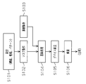
- FIG. 9 is a flowchart illustrating a manufacturing example of a micro device (a semiconductor chip such as an IC or LSI, a liquid crystal panel, a CCD, a thin film magnetic head, a micromachine, or the like).
- a micro device a semiconductor chip such as an IC or LSI, a liquid crystal panel, a CCD, a thin film magnetic head, a micromachine, or the like.
- step S101 design step
- function / performance design of a micro device for example, circuit design of a semiconductor device
- a pattern design for realizing the function is performed.
- step S102 mask manufacturing step
- a mask reticle R or the like
- step S103 substrate manufacturing step
- a substrate a wafer W when a silicon material is used
- a material such as silicon, glass, or ceramics.
- step S104 substrate processing step
- step S105 device assembly step
- step S105 includes processes such as a dicing process, a bonding process, and a packaging process (chip encapsulation) as necessary.
- step S106 inspection step
- inspections such as an operation confirmation test and a durability test of the microdevice manufactured in step S105 are performed. After these steps, the microdevice is completed and shipped.
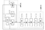
- FIG. 10 is a diagram illustrating an example of a detailed process of step S104 in the case of a semiconductor device.
- step S111 oxidation step
- step S112 CVD step
- step S113 electrode formation step
- step S114 ion implantation step
- ions are implanted into the substrate.
- step S115 resist formation step
- step S116 exposure step
- step S116 exposure step
- step S117 development step
- step S118 etching step
- step S119 resist removal step
- the photosensitive material that has become unnecessary after the etching is removed. That is, in step S118 and step S119, the surface of the substrate is processed through the mask layer.
- SYMBOLS 11 Exposure apparatus, 12 ... Illumination optical system, 14 ... Projection optical system, 15, 15A ... Wafer stage as a holding device, 17 ... Lens tube as a support member, 18-23 ... Other optical members, As a movable optical member 24 ... a holding device as an optical member holding device, 27 ... an image surface side optical member, 30 ... an exit side surface as an optical surface on the image surface side, 36 ... a predetermined space, 37, 37A ... a liquid as a polishing device. Supply device, 38 ... holding part, 43 ... liquid recovery part constituting the recovery part, 46 ... switching part, 52, 60 ... supply nozzle, 53 ...
- recovery nozzle constituting the recovery part, 62 ... displacement part, 65, 67, 76, 80: Polishing device, 66: Spray nozzle, 68: Polishing pad, 77: Polishing part, EL: Exposure light, W: Wafer as substrate.
Landscapes
- Physics & Mathematics (AREA)
- General Physics & Mathematics (AREA)
- Exposure And Positioning Against Photoresist Photosensitive Materials (AREA)
- Exposure Of Semiconductors, Excluding Electron Or Ion Beam Exposure (AREA)
Abstract
Description
本発明の1つの態様にかかる露光装置は、所定のパターンを光(EL)で照明し、該所定のパターンを介した光(EL)で感光性材料が塗布された基板(W)を照射する露光装置(11)であって、前記光(EL)の光路に配置される光学部材(18,19,20,21,22,23,27)及び該光学部材(18,19,20,21,22,23,27)を支持する支持部材(17)を有する光学系(12,14)と、前記支持部材(17)に支持されている状態の前記光学部材(18,19,20,21,22,23,27)を研磨し、該光学部材(18,19,20,21,22,23,27)の形状を変化させる研磨装置(37,37A,65,67,76,80)と、を備えることを要旨とする。
図1に示すように、液体供給装置37は、露光処理時などに用いられる第1液体(例えば純水)を所定空間36内に供給すべく駆動する第1液体供給部41と、像面側光学部材27の研磨時などに用いられる第2液体(例えば、研磨剤を含有する液体)を供給すべく駆動する第2液体供給部42とを備えている。また、液体供給装置37には、所定空間36内の液体を回収すべく駆動する液体回収部43と、液体供給部41,42から延びる供給管44,45がそれぞれ接続される切替部46とが設けられている。この切替部46は、2つの入力ポートと1つの出力ポートとを有する図示しない切替弁を備えており、該切替弁の駆動によって後述する液体供給回収部材47への供給を許容する液体の種類が選択される。
(1)鏡筒17に支持されている状態の像面側光学部材27を液体供給装置37によって変形させることにより、投影光学系14の収差が調整される。したがって、投影光学系14から光学部材を取り出し、該光学部材の形状を変更させる従来の場合に比して、投影光学系14から光学部材を取り出す手間が省ける分、短時間で投影光学系14の収差を容易に調整でき、ひいては露光装置11の稼動停止時間を短縮して生産性の向上を図ることができる。
・実施形態において、液体供給装置は、露光処理時と研磨時とで液体の噴射方向を変更可能な構成であってもよい。例えば、図4(a)(b)に示すように、液体供給装置37Aは、像面側光学部材27の露光光通過部29を包囲するように配置される複数(図4(a)では2つのみ図示)の供給ノズル60と、該各供給ノズル60に第1液体又は第2液体を供給する液体供給通路61とを備えている。また、液体供給装置37Aには、各供給ノズル(噴射ノズル)60を、ウエハステージ15に向けて液体を供給する第1位置(図3(a)に示す位置)と、像面側光学部材27の射出側面30の周縁部30aに向けて液体を供給する第2位置(図3(b)に示す位置)との間で変位させるための変位部62が設けられている。そして、露光処理時には、変位部62の駆動によって各供給ノズル60が第1位置に配置され、その後、各供給ノズル60からは、第1液体が噴射される。その結果、所定空間36内に第1液体が充填される。
・実施形態において、露光装置11は、半導体素子などのマイクロデバイスだけでなく、光露光装置、EUV露光装置、X線露光装置、及び電子線露光装置などで使用されるレチクルまたはマスクを製造するために、マザーレチクルからガラス基板やシリコンウエハなどへ回路パターンを転写する露光装置であってもよい。また、露光装置11は、液晶表示素子(LCD)などを含むディスプレイの製造に用いられてデバイスパターンをガラスプレート上へ転写する露光装置、薄膜磁気ヘッド等の製造に用いられて、デバイスパターンをセラミックウエハ等へ転写する露光装置、及びCCD等の撮像素子の製造に用いられる露光装置などであってもよい。
・実施形態において、可変パターン生成器(例えば、DMD(Digital Mirror Device又はDigital Micro-mirror Device))を用いたマスクレス露光装置に具体化してもよい。このようなマスクレス露光装置は、例えば特開2004-304135号公報、国際特許公開第2006/080285号パンフレット及びこれに対応する米国特許公開第2007/0296936号公報に開示されている。
ステップS111(酸化ステップ)においては、基板の表面を酸化させる。ステップS112(CVDステップ)においては、基板表面に絶縁膜を形成する。ステップS113(電極形成ステップ)においては、基板上に電極を蒸着によって形成する。ステップS114(イオン打込みステップ)においては、基板にイオンを打ち込む。以上のステップS111~ステップS114のそれぞれは、基板処理の各段階の前処理工程を構成しており、各段階において必要な処理に応じて選択されて実行される。
Claims (40)
- 所定のパターンを光で照明し、該所定のパターンを介した光で感光性材料が塗布された基板を照射する露光装置であって、
前記光の光路に配置される光学部材及び該光学部材を支持する支持部材を有する光学系と、
前記支持部材に支持されている状態の前記光学部材を研磨し、該光学部材の形状を変化させる研磨装置と、を備えることを特徴とする露光装置。 - 前記光学系は、前記光学部材を複数有しており、
前記研磨装置は、前記光学部材のうち最も像面側に位置する像面側光学部材の像面側の光学面を研磨することを特徴とする請求項1に記載の露光装置。 - 前記光学系は、前記所定のパターンを介した光を前記基板に導く投影光学系であると共に、
前記基板を保持する保持部を有する保持装置と、
前記像面側光学部材と前記保持部との間に設けられる空間内を液密状態にする液体供給装置と、をさらに備え、
該液体供給装置は、前記光が透過可能な液体を前記光学部材に向けて噴射可能な供給ノズルを有し、前記液体供給装置が、前記研磨装置として機能することを特徴とする請求項2に記載の露光装置。 - 前記液体供給装置は、前記供給ノズルから噴射された液体を回収する回収部をさらに有することを特徴とする請求項3に記載の露光装置。
- 前記液体供給装置は、前記供給ノズルから噴射される液体の単位時間あたりの噴射量を調整可能であることを特徴とする請求項3又は請求項4に記載の露光装置。
- 前記液体供給装置は、液体の噴射方向が変更されるように前記供給ノズルを変位させる変位部をさらに有することを特徴とする請求項3~請求項5のうち何れか一項に記載の露光装置。
- 前記液体供給装置は、前記供給ノズルから噴射する液体を、前記光が透過可能な第1の液体と、前記第1の液体とは異なる第2の液体とで切り替えるための切替部をさらに有することを特徴とする請求項3~請求項6のうち何れか一項に記載の露光装置。
- 前記研磨装置は、研磨用液体を前記光学部材に向けて噴射する噴射ノズルを有することを特徴とする請求項1又は請求項2に記載の露光装置。
- 前記光学系は、前記所定のパターンを介した光を前記基板に導く投影光学系であると共に、
前記基板を保持する保持部を有する保持装置をさらに備え、
前記噴射ノズルは、前記保持装置側から前記光学部材に向けて研磨用液体を噴射することを特徴とする請求項8に記載の露光装置。 - 前記研磨装置は、前記光学部材の光学面の周縁部の側方に配置され、前記周縁部に向けて研磨用液体をほぼ同時にほぼ同じ噴射圧で噴射する複数の供給ノズルを有する請求項1又は2に記載の露光装置。
- 前記研磨装置は、前記光学部材の光学面に対面し、前記光学面に向けて研磨用液体を制御されたタイミングで制御された噴射圧で噴射する複数の供給ノズルを有する請求項1又は2に記載の露光装置。
- 前記研磨装置は、前記複数の供給ノズルからの前記研磨用液体の噴射を制御する制御装置を含む請求項10又は11に記載の露光装置。
- 前記光学系は、前記像面側光学部材とは異なる他の光学部材を保持すると共に、該他の光学部材を前記支持部材に対して変位させることが可能な光学部材保持装置をさらに有することを特徴とする請求項2に記載の露光装置。
- 前記光学系は、前記所定のパターンを介した光を前記基板に導く投影光学系であると共に、
前記基板を保持する保持部を有する保持装置と、
前記像面側光学部材と前記保持部との間に設けられる空間内を液密状態にする液体供給装置と、をさらに備えることを特徴とする請求項2~請求項13のうち何れか一項に記載の露光装置。 - 前記像面側光学部材の像面側の光学面は、無コートであることを特徴とする請求項2~請求項14のうち何れか一項に記載の露光装置。
- 請求項1~請求項15のうち何れか一項に記載の露光装置を用いて、前記所定のパターンに基づくパターン像を前記基板の表面に露光し、
露光された前記基板を現像して前記パターン像に対応する形状のマスク層を前記基板の表面に形成し、
前記基板の前記表面に形成された前記マスク層を介して前記基板の表面を加工することを特徴とするデバイスの製造方法。 - 所定のパターンを光で照明し、該所定のパターンを介した光で感光性材料が塗布された基板を照射する露光装置であって、前記光の光路に配置される光学部材及び該光学部材を支持する支持部材を有する光学系を備える露光装置に取付けられる研磨装置であって、
前記支持部材に支持されている状態の前記光学部材を研磨し、該光学部材の形状を変化させることを特徴とする研磨装置。 - 前記光学系は、前記光学部材を複数有しており、
前記研磨装置は、前記光学部材のうち最も像面側に位置する像面側光学部材の像面側の光学面を研磨することを特徴とする請求項17に記載の研磨装置。 - 前記光学系は、前記所定のパターンを介した光を前記基板に導く投影光学系であって、且つ前記光学部材を複数有しており、
前記露光装置は、前記基板を保持する保持部を有する保持装置と、前記光学部材のうち最も像面側に位置する像面側光学部材と前記保持部との間に設けられる空間内を液密状態にする液体供給装置と、をさらに備えることを特徴とする請求項17又は請求項18に記載の研磨装置。 - 前記像面側光学部材の像面側の光学面に向けて媒質を噴射可能な供給ノズルを有することを特徴とする請求項19に記載の研磨装置。
- 前記供給ノズルから噴射された媒質を回収する回収部をさらに有することを特徴とする請求項20に記載の研磨装置。
- 前記供給ノズルから噴射される媒質の単位時間あたりの噴射量を調整可能であることを特徴とする請求項20又は請求項21に記載の研磨装置。
- 媒質の噴射方向が変更されるように前記供給ノズルを変位させる変位部をさらに有することを特徴とする請求項20~請求項22のうち何れか一項に記載の研磨装置。
- 前記像面側光学部材の像面側の光学面に接触可能な研磨パッドを有することを特徴とする請求項19に記載の研磨装置。
- 前記像面側光学部材の前記像面側の前記光学面は、無コートであることを特徴とする請求項18~請求項24のうち何れか一項に記載の研磨装置。
- 請求項17~請求項25のうち何れか一項に記載の研磨装置を備えることを特徴とする露光装置。
- 請求項26に記載の露光装置を用いて、前記所定のパターンに基づくパターン像を前記基板の表面に露光し、
露光された前記基板を現像して前記パターン像に対応する形状のマスク層を前記基板の表面に形成し、
前記基板の前記表面に形成された前記マスク層を介して前記基板の表面を加工することを特徴とするデバイスの製造方法。 - 所定のパターンを光で照明し、該所定のパターンを介した光で感光性材料が塗布された基板を照射する露光装置であって、前記光の光路に配置される光学部材及び該光学部材を支持する支持部材を有する光学系を備える露光装置の前記光学部材を研磨する研磨方法であって、
前記支持部材に支持されている状態の前記光学部材を研磨し、該光学部材の形状を変化させることを特徴とする研磨方法。 - 前記光学系は、前記光学部材を複数有しており、
前記光学部材のうち最も像面側に位置する像面側光学部材の像面側の光学面を研磨することを特徴とする請求項28に記載の研磨方法。 - 前記光学系は、前記所定のパターンを介した光を前記基板に導く投影光学系であって、且つ前記光学部材を複数有しており、
前記露光装置は、前記基板を保持する保持部を有する保持装置と、前記光学部材のうち最も像面側に位置する像面側光学部材と前記保持部との間に設けられる空間内を液密状態にする液体供給装置と、をさらに備えることを特徴とする請求項28又は請求項29に記載の研磨方法。 - 前記像面側光学部材の像面側の光学面に向けて媒質を噴射することを特徴とする請求項29又は請求項30に記載の研磨方法。
- 前記噴射された媒質を回収することを特徴とする請求項31に記載の研磨装置。
- 前記噴射される媒質の単位時間あたりの噴射量を調整することを特徴とする請求項31又は請求項32に記載の研磨方法。
- 媒質の噴射方向を変更することを特徴とする請求項31~請求項33のうち何れか一項に記載の研磨方法。
- 前記光学系は、前記光学部材を複数有しており、
前記光学部材のうち最も像面側に位置する像面側光学部材の像面側の光学面を研磨パッドで研磨することを特徴とする請求項28又は請求項29に記載の研磨方法。 - 前記光学系は、前記光学部材を複数有しており、
前記光学部材のうち最も像面側に位置する像面側光学部材の像面側の光学面は、無コートであることを特徴とする請求項28~請求項35のうち何れか一項に記載の研磨方法。 - 前記光学部材の面形状を計測し、該計測結果に基づいて前記光学部材の形状を変化させることを特徴とする請求項28~請求項35のうち何れか一項に記載の研磨方法。
- 前記光学系は、前記所定のパターンを介した光を前記基板に導く投影光学系であり、該投影光学系の収差を調整するために前記光の光路に位置調整可能に配置される可動光学部材をさらに備え、
該可動光学部材によって調整可能な前記投影光学系の収差の範囲が所定範囲を超えるか否かを判定することを特徴とする請求項28~請求項37のうち何れか一項に記載の研磨方法。 - 前記判定結果が前記所定範囲を超える場合に、前記支持部材に支持されている状態の前記光学部材を研磨して前記光学部材の形状を変化させることを特徴とする請求項38に記載の研磨方法。
- 所定のパターンを光で照明し、該所定のパターンを介した光で感光性材料が塗布された基板を照射する露光装置であって、前記光の光路に配置される光学部材及び該光学部材を支持する支持部材を有する光学系を備える露光装置を用いて、所定のパターンに基づくパターン像を前記基板の表面に露光し、露光された前記基板を現像して前記パターン像に対応する形状のマスク層を前記基板の表面に形成し、前記基板の前記表面に形成された前記マスク層を介して前記基板の表面を加工することを特徴とするデバイスの製造方法であって、
前記基板の表面に露光する時間とは別の時間に、請求項28~請求項39の何れか一項に記載の研磨方法を用いて、前記支持部材に支持されている状態の前記光学部材を研磨し、該光学部材の形状を変化させることを特徴とするデバイスの製造方法。
Priority Applications (3)
| Application Number | Priority Date | Filing Date | Title |
|---|---|---|---|
| JP2011520823A JPWO2011001740A1 (ja) | 2009-07-01 | 2010-05-07 | 研磨装置、研磨方法、露光装置及びデバイスの製造方法 |
| DE112010002795T DE112010002795T5 (de) | 2009-07-01 | 2010-05-07 | Schleifvorrichtung, Schleifverfahren, Belichtungsvorrichtung undVerfahren zum Herstellen eines Bauelements |
| US13/225,061 US20120062859A1 (en) | 2009-07-01 | 2011-09-02 | Polishing device, polishing method, exposure apparatus and device manufacturing method |
Applications Claiming Priority (2)
| Application Number | Priority Date | Filing Date | Title |
|---|---|---|---|
| US21367609P | 2009-07-01 | 2009-07-01 | |
| US61/213,676 | 2009-07-01 |
Related Child Applications (1)
| Application Number | Title | Priority Date | Filing Date |
|---|---|---|---|
| US13/225,061 Continuation US20120062859A1 (en) | 2009-07-01 | 2011-09-02 | Polishing device, polishing method, exposure apparatus and device manufacturing method |
Publications (1)
| Publication Number | Publication Date |
|---|---|
| WO2011001740A1 true WO2011001740A1 (ja) | 2011-01-06 |
Family
ID=43410824
Family Applications (1)
| Application Number | Title | Priority Date | Filing Date |
|---|---|---|---|
| PCT/JP2010/057813 Ceased WO2011001740A1 (ja) | 2009-07-01 | 2010-05-07 | 研磨装置、研磨方法、露光装置及びデバイスの製造方法 |
Country Status (6)
| Country | Link |
|---|---|
| US (1) | US20120062859A1 (ja) |
| JP (1) | JPWO2011001740A1 (ja) |
| KR (1) | KR20120026471A (ja) |
| DE (1) | DE112010002795T5 (ja) |
| TW (1) | TW201102765A (ja) |
| WO (1) | WO2011001740A1 (ja) |
Cited By (1)
| Publication number | Priority date | Publication date | Assignee | Title |
|---|---|---|---|---|
| WO2013156477A1 (en) | 2012-04-18 | 2013-10-24 | 3B Fibreglass Sprl | Glass fibre composition and composite material reinforced therewith |
Families Citing this family (1)
| Publication number | Priority date | Publication date | Assignee | Title |
|---|---|---|---|---|
| JP6493087B2 (ja) | 2015-08-24 | 2019-04-03 | 株式会社デンソー | 車載カメラ装置 |
Citations (7)
| Publication number | Priority date | Publication date | Assignee | Title |
|---|---|---|---|---|
| JP2005072404A (ja) * | 2003-08-27 | 2005-03-17 | Sony Corp | 露光装置および半導体装置の製造方法 |
| JP2005079222A (ja) * | 2003-08-29 | 2005-03-24 | Nikon Corp | 光学部品の洗浄機構を搭載した液浸投影露光装置及び液浸光学部品洗浄方法 |
| JP2005277363A (ja) * | 2003-05-23 | 2005-10-06 | Nikon Corp | 露光装置及びデバイス製造方法 |
| JP2006073951A (ja) * | 2004-09-06 | 2006-03-16 | Toshiba Corp | 液浸光学装置及び洗浄方法 |
| JP2006523031A (ja) * | 2003-04-11 | 2006-10-05 | 株式会社ニコン | 液浸リソグラフィにおける光学素子の洗浄方法 |
| JP2008205038A (ja) * | 2007-02-16 | 2008-09-04 | Canon Inc | 露光装置及びデバイス製造方法 |
| JP2008300775A (ja) * | 2007-06-04 | 2008-12-11 | Nikon Corp | クリーニング装置、クリーニング方法、露光装置、及びデバイス製造方法 |
Family Cites Families (20)
| Publication number | Priority date | Publication date | Assignee | Title |
|---|---|---|---|---|
| JPH06124873A (ja) | 1992-10-09 | 1994-05-06 | Canon Inc | 液浸式投影露光装置 |
| JP3747566B2 (ja) | 1997-04-23 | 2006-02-22 | 株式会社ニコン | 液浸型露光装置 |
| WO1999027568A1 (en) | 1997-11-21 | 1999-06-03 | Nikon Corporation | Projection aligner and projection exposure method |
| WO1999049504A1 (fr) | 1998-03-26 | 1999-09-30 | Nikon Corporation | Procede et systeme d'exposition par projection |
| JP4945845B2 (ja) | 2000-03-31 | 2012-06-06 | 株式会社ニコン | 光学素子保持装置、鏡筒及び露光装置並びにマイクロデバイスの製造方法。 |
| JP4345098B2 (ja) | 2001-02-06 | 2009-10-14 | 株式会社ニコン | 露光装置及び露光方法、並びにデバイス製造方法 |
| JP2002372406A (ja) | 2001-06-13 | 2002-12-26 | Nikon Corp | 位置検出装置及び方法、位置検出装置の収差測定方法及び調整方法、露光装置、並びにマイクロデバイスの製造方法 |
| WO2004050266A1 (ja) | 2002-12-03 | 2004-06-17 | Nikon Corporation | 汚染物質除去方法及び装置、並びに露光方法及び装置 |
| JP2004304135A (ja) | 2003-04-01 | 2004-10-28 | Nikon Corp | 露光装置、露光方法及びマイクロデバイスの製造方法 |
| TW201834020A (zh) | 2003-10-28 | 2018-09-16 | 日商尼康股份有限公司 | 照明光學裝置、曝光裝置、曝光方法以及元件製造方法 |
| WO2005064382A1 (ja) | 2003-12-25 | 2005-07-14 | Nikon Corporation | 光学素子の保持装置、鏡筒、露光装置、及びデバイスの製造方法 |
| TWI389174B (zh) | 2004-02-06 | 2013-03-11 | 尼康股份有限公司 | 偏光變換元件、光學照明裝置、曝光裝置以及曝光方法 |
| JP4341432B2 (ja) | 2004-03-08 | 2009-10-07 | 株式会社ニコン | 研磨装置および研磨加工方法 |
| JP2005246590A (ja) | 2004-03-08 | 2005-09-15 | Nikon Corp | 噴射ノズル、研磨装置、研磨方法、光学素子及び露光装置 |
| EP1737024A4 (en) | 2004-03-25 | 2008-10-15 | Nikon Corp | Exposure equipment, exposure method and device manufacturing method |
| KR101280166B1 (ko) | 2004-11-25 | 2013-06-28 | 가부시키가이샤 니콘 | 이동체 시스템, 노광 장치 및 디바이스 제조 방법 |
| TWI453796B (zh) | 2005-01-21 | 2014-09-21 | 尼康股份有限公司 | 偏光變更單元以及元件製造方法 |
| JP4858439B2 (ja) | 2005-01-25 | 2012-01-18 | 株式会社ニコン | 露光装置及び露光方法並びにマイクロデバイスの製造方法 |
| JP2006245085A (ja) | 2005-03-01 | 2006-09-14 | Nikon Corp | 投影光学系、投影光学系の調整方法、露光装置、および露光方法 |
| EP3267258A1 (en) | 2006-02-21 | 2018-01-10 | Nikon Corporation | Exposure apparatus, exposure method and device manufacturing method |
-
2010
- 2010-04-26 TW TW099113097A patent/TW201102765A/zh unknown
- 2010-05-07 DE DE112010002795T patent/DE112010002795T5/de not_active Withdrawn
- 2010-05-07 KR KR1020117020581A patent/KR20120026471A/ko not_active Withdrawn
- 2010-05-07 JP JP2011520823A patent/JPWO2011001740A1/ja active Pending
- 2010-05-07 WO PCT/JP2010/057813 patent/WO2011001740A1/ja not_active Ceased
-
2011
- 2011-09-02 US US13/225,061 patent/US20120062859A1/en not_active Abandoned
Patent Citations (7)
| Publication number | Priority date | Publication date | Assignee | Title |
|---|---|---|---|---|
| JP2006523031A (ja) * | 2003-04-11 | 2006-10-05 | 株式会社ニコン | 液浸リソグラフィにおける光学素子の洗浄方法 |
| JP2005277363A (ja) * | 2003-05-23 | 2005-10-06 | Nikon Corp | 露光装置及びデバイス製造方法 |
| JP2005072404A (ja) * | 2003-08-27 | 2005-03-17 | Sony Corp | 露光装置および半導体装置の製造方法 |
| JP2005079222A (ja) * | 2003-08-29 | 2005-03-24 | Nikon Corp | 光学部品の洗浄機構を搭載した液浸投影露光装置及び液浸光学部品洗浄方法 |
| JP2006073951A (ja) * | 2004-09-06 | 2006-03-16 | Toshiba Corp | 液浸光学装置及び洗浄方法 |
| JP2008205038A (ja) * | 2007-02-16 | 2008-09-04 | Canon Inc | 露光装置及びデバイス製造方法 |
| JP2008300775A (ja) * | 2007-06-04 | 2008-12-11 | Nikon Corp | クリーニング装置、クリーニング方法、露光装置、及びデバイス製造方法 |
Cited By (1)
| Publication number | Priority date | Publication date | Assignee | Title |
|---|---|---|---|---|
| WO2013156477A1 (en) | 2012-04-18 | 2013-10-24 | 3B Fibreglass Sprl | Glass fibre composition and composite material reinforced therewith |
Also Published As
| Publication number | Publication date |
|---|---|
| TW201102765A (en) | 2011-01-16 |
| JPWO2011001740A1 (ja) | 2012-12-13 |
| DE112010002795T5 (de) | 2012-08-23 |
| US20120062859A1 (en) | 2012-03-15 |
| KR20120026471A (ko) | 2012-03-19 |
Similar Documents
| Publication | Publication Date | Title |
|---|---|---|
| JP4582089B2 (ja) | 液浸リソグラフィ用の液体噴射回収システム | |
| JP6469761B2 (ja) | リソグラフィ装置及びデバイス製造方法 | |
| CN101385124B (zh) | 维修方法、曝光方法及装置、以及组件制造方法 | |
| JP4510494B2 (ja) | 露光装置 | |
| US8189168B2 (en) | Exposure apparatus, device production method, cleaning apparatus, cleaning method, and exposure method | |
| CN101390194A (zh) | 维修方法、曝光方法及装置、以及元件制造方法 | |
| JP5249381B2 (ja) | 基板テーブル、リソグラフィ装置、基板のエッジを平らにする方法、及びデバイス製造方法 | |
| KR101506054B1 (ko) | 노광 장치 및 노광 방법 | |
| JP6456476B2 (ja) | リソグラフィ装置及びデバイスを製造する方法 | |
| JP2012043992A (ja) | 清掃装置、清掃方法、露光装置、露光方法及びデバイスの製造方法 | |
| WO2011001740A1 (ja) | 研磨装置、研磨方法、露光装置及びデバイスの製造方法 | |
| JP2006202825A (ja) | 液浸型露光装置 | |
| JP2012099567A (ja) | 洗浄方法および露光装置 | |
| JP2008263091A (ja) | 光洗浄部材、メンテナンス方法、洗浄方法、露光方法及び露光装置、並びにデバイス製造方法 | |
| JP2012009668A (ja) | チタン含有部材の製造方法、チタン含有部材、露光装置及びデバイス製造方法 | |
| JP2005079480A (ja) | 露光装置及びデバイス製造方法 | |
| WO2005081294A1 (ja) | 露光装置、液体処理方法、露光方法、及びデバイス製造方法 | |
| JP2010267808A (ja) | 露光装置、クリーニング方法、及びデバイス製造方法 | |
| JP2009021365A (ja) | 露光装置、デバイス製造方法、メンテナンス方法、及び膜形成装置 | |
| JP2003124098A (ja) | 露光装置 | |
| JP2003203847A (ja) | 露光装置 | |
| JP2006332531A (ja) | 投影光学系、露光装置、及びデバイスの製造方法 | |
| JP2011066066A (ja) | 露光装置及び洗浄方法 |
Legal Events
| Date | Code | Title | Description |
|---|---|---|---|
| 121 | Ep: the epo has been informed by wipo that ep was designated in this application |
Ref document number: 10793911 Country of ref document: EP Kind code of ref document: A1 |
|
| WWE | Wipo information: entry into national phase |
Ref document number: 2011520823 Country of ref document: JP |
|
| ENP | Entry into the national phase |
Ref document number: 20117020581 Country of ref document: KR Kind code of ref document: A |
|
| WWE | Wipo information: entry into national phase |
Ref document number: 112010002795 Country of ref document: DE Ref document number: 1120100027951 Country of ref document: DE |
|
| 122 | Ep: pct application non-entry in european phase |
Ref document number: 10793911 Country of ref document: EP Kind code of ref document: A1 |