WO2010150595A1 - 積層構造体及びその製造方法 - Google Patents
積層構造体及びその製造方法 Download PDFInfo
- Publication number
- WO2010150595A1 WO2010150595A1 PCT/JP2010/057818 JP2010057818W WO2010150595A1 WO 2010150595 A1 WO2010150595 A1 WO 2010150595A1 JP 2010057818 W JP2010057818 W JP 2010057818W WO 2010150595 A1 WO2010150595 A1 WO 2010150595A1
- Authority
- WO
- WIPO (PCT)
- Prior art keywords
- dielectric
- layer
- conductive layer
- laminated structure
- underlayer
- Prior art date
- Legal status (The legal status is an assumption and is not a legal conclusion. Google has not performed a legal analysis and makes no representation as to the accuracy of the status listed.)
- Ceased
Links
Images


Classifications
-
- H—ELECTRICITY
- H05—ELECTRIC TECHNIQUES NOT OTHERWISE PROVIDED FOR
- H05K—PRINTED CIRCUITS; CASINGS OR CONSTRUCTIONAL DETAILS OF ELECTRIC APPARATUS; MANUFACTURE OF ASSEMBLAGES OF ELECTRICAL COMPONENTS
- H05K1/00—Printed circuits
- H05K1/16—Printed circuits incorporating printed electric components, e.g. printed resistors, capacitors or inductors
- H05K1/162—Printed circuits incorporating printed electric components, e.g. printed resistors, capacitors or inductors incorporating printed capacitors
-
- H—ELECTRICITY
- H01—ELECTRIC ELEMENTS
- H01G—CAPACITORS; CAPACITORS, RECTIFIERS, DETECTORS, SWITCHING DEVICES, LIGHT-SENSITIVE OR TEMPERATURE-SENSITIVE DEVICES OF THE ELECTROLYTIC TYPE
- H01G4/00—Fixed capacitors; Processes of their manufacture
- H01G4/002—Details
- H01G4/018—Dielectrics
- H01G4/06—Solid dielectrics
- H01G4/08—Inorganic dielectrics
- H01G4/12—Ceramic dielectrics
- H01G4/1209—Ceramic dielectrics characterised by the ceramic dielectric material
-
- H—ELECTRICITY
- H01—ELECTRIC ELEMENTS
- H01G—CAPACITORS; CAPACITORS, RECTIFIERS, DETECTORS, SWITCHING DEVICES, LIGHT-SENSITIVE OR TEMPERATURE-SENSITIVE DEVICES OF THE ELECTROLYTIC TYPE
- H01G4/00—Fixed capacitors; Processes of their manufacture
- H01G4/30—Stacked capacitors
-
- H—ELECTRICITY
- H01—ELECTRIC ELEMENTS
- H01G—CAPACITORS; CAPACITORS, RECTIFIERS, DETECTORS, SWITCHING DEVICES, LIGHT-SENSITIVE OR TEMPERATURE-SENSITIVE DEVICES OF THE ELECTROLYTIC TYPE
- H01G4/00—Fixed capacitors; Processes of their manufacture
- H01G4/33—Thin- or thick-film capacitors (thin- or thick-film circuits; capacitors without a potential-jump or surface barrier specially adapted for integrated circuits, details thereof, multistep manufacturing processes therefor)
-
- H—ELECTRICITY
- H05—ELECTRIC TECHNIQUES NOT OTHERWISE PROVIDED FOR
- H05K—PRINTED CIRCUITS; CASINGS OR CONSTRUCTIONAL DETAILS OF ELECTRIC APPARATUS; MANUFACTURE OF ASSEMBLAGES OF ELECTRICAL COMPONENTS
- H05K2201/00—Indexing scheme relating to printed circuits covered by H05K1/00
- H05K2201/01—Dielectrics
- H05K2201/0183—Dielectric layers
- H05K2201/0195—Dielectric or adhesive layers comprising a plurality of layers, e.g. in a multilayer structure
-
- H—ELECTRICITY
- H05—ELECTRIC TECHNIQUES NOT OTHERWISE PROVIDED FOR
- H05K—PRINTED CIRCUITS; CASINGS OR CONSTRUCTIONAL DETAILS OF ELECTRIC APPARATUS; MANUFACTURE OF ASSEMBLAGES OF ELECTRICAL COMPONENTS
- H05K2203/00—Indexing scheme relating to apparatus or processes for manufacturing printed circuits covered by H05K3/00
- H05K2203/13—Moulding and encapsulation; Deposition techniques; Protective layers
- H05K2203/1333—Deposition techniques, e.g. coating
- H05K2203/1355—Powder coating of insulating material
Definitions
- This type of laminated structure is configured by interposing a dielectric film between the first conductive layer and the second conductive layer, and the dielectric film may be a sol-gel method, an MOCVD method, a sputtering vapor deposition method, or the like. Was formed on the first conductive layer.
- the dielectric film is first formed by using various powder spray coating methods such as a powder jet deposition method and an aerosol deposition method. It is considered to form by spraying on the surface of the conductive layer.
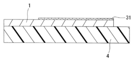
- the dielectric film is formed on the surface of the first conductive layer using the powder spray coating method, the surface of the first conductive layer is etched by the collision of the dielectric powder, and as shown in FIG. There was a problem that irregularities were formed on the surface.
- the dielectric film thickness becomes non-uniform, which causes the film thickness to become very small in a part of the dielectric film, or as shown in FIG. A part of the first conductive layer is exposed on the surface, and the insulating property of the laminated structure may be lowered.
- an object of the present invention is to suppress a decrease in insulation in a laminated structure in which a dielectric film is formed using a powder spray coating method and a manufacturing method thereof.
- a manufacturing method of a laminated structure according to the present invention is a manufacturing method of a laminated structure in which a dielectric layer is interposed between a first conductive layer and a second conductive layer, and a dielectric is formed on the first conductive layer.
- the dielectric layer forming step includes forming a base layer by applying a dispersion solution containing dielectric fine particles on the first conductive layer, and powder spray coating on the base layer.
- a dielectric film forming step of forming a dielectric film by a method is a method of a laminated structure in which a dielectric layer is interposed between a first conductive layer and a second conductive layer, and a dielectric is formed on the first conductive layer.
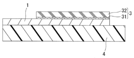
- the dielectric layer (3) includes a base layer (31) formed on the first conductive layer (1) and a dielectric film (32) formed on the base layer (31). .
- the underlayer (31) is formed by applying a dispersion solution containing dielectric fine particles containing barium titanate (BaTiO3) as a main component on the first conductive layer (1).
- the dispersion solution is prepared by adding dielectric fine particles and a dispersant to a solvent without using a binder, and the sol-gel method is used for the preparation.
- the dielectric fine particles contained in the dispersion solution are nanoparticles having an average particle diameter of 50 nm or less, and the dispersion layer applied on the first conductive layer (1) is dried in the underlayer (31).
- the thin film is formed by agglomeration of dielectric fine particles.
- the dielectric film (32) is formed by spraying a dielectric powder containing barium titanate (BaTiO3) as a main component on the surface of the underlayer (31) by a powder spray coating method. Details of the powder spray coating method will be described later.
- dielectric materials having different main components may be used for the dielectric fine particles and the dielectric film (32) constituting the underlayer (31).
- the dielectric fine particles and the dielectric film (32) constituting the base layer (31) may contain additives in order to improve dielectric properties, insulating properties, strength, and the like.
- the second conductive layer (2) is a metal film formed on the dielectric layer (3) by sputtering deposition, plating, screen printing or the like, or a metal attached on the dielectric layer (3).
- the foil is made of a metal such as copper (Cu), nickel (Ni), cobalt (Co), gold (Au), platinum (Pt), etc., like the first conductive layer (1).
- a formation process is performed in this order.
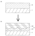
- the dielectric layer forming step includes a base layer forming step of forming a base layer (31) on the first conductive layer (1) as shown in FIG. 2, and a dielectric layer on the base layer (31) as shown in FIG. And a dielectric film forming step for forming the body film (32).
- a dispersion solution containing dielectric fine particles mainly composed of barium titanate (BaTiO3) is applied on the first conductive layer (1), and the dispersion solution is dried to form an underlayer (31 ).
- the underlayer (31) is formed to be thicker than the thickness that will be etched in the dielectric film forming step described later.
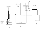
- a dielectric film is formed by aerosolizing dielectric powder using a film forming apparatus as shown in FIG. 4 and spraying the powder toward the surface on which the dielectric film is to be formed. Is the law.
- the film forming apparatus can maintain the inside in a vacuum state by an aerosol generator (71) that stirs and mixes dielectric powder with a high-pressure gas to form an aerosol, and a vacuum pump (73).
- a possible film forming chamber (72) is connected by a thin transfer tube (74).
- the space (high pressure space) in the aerosol generator (71) into which the high pressure gas flows and the film formation chamber (72) A pressure difference is generated between the space (low pressure space). Therefore, the dielectric powder aerosolized by the aerosol generator (71) flows in the transfer tube (74) toward the film forming chamber (72).
- the dielectric powder discharged at high speed from the tip of the nozzle (76) is sprayed onto the surface of the object on the stage (75).
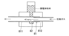
- the powder jet deposition method is a film forming method in which a dielectric film is formed by injecting a dielectric powder toward a surface on which a dielectric film is to be formed using an injection device as shown in FIG.
- the injection device includes a stepped nozzle (81) having two regions (811) and (812) having different inner diameters.
- the nozzle (81) includes a first region (811 having a larger inner diameter).
- a through hole (82) for supplying dielectric powder is formed at a position close to the second region (812) having a small inner diameter.
- the underlayer (31) Barium titanate (BaTiO3) dielectric powder having a particle size of about 1 ⁇ m is sprayed onto the surface.
- the dielectric powder sprayed on the surface of the underlayer (31) collides with the surface of the underlayer (31) or other dielectric powder and is crushed and deposited on the underlayer (31), thereby A dielectric film (32) is formed on the base layer (31). Therefore, the dielectric film (32) formed using the powder spray coating method becomes a dense bulk film.
- a metal film is formed on the dielectric film (32) formed in the dielectric film forming step using a sputtering vapor deposition method, a plating method, a screen printing method, or the like, or a dielectric film ( 32)
- a second conductive layer (2) is formed by attaching a metal foil on top.
- the ground layer (31) is formed on the surface of the first conductive layer (1) on which the dielectric film (32) is to be formed.
- the applied dielectric powder collides with the underlayer (31), and the surface of the first conductive layer (1) is protected from the collision of the dielectric powder by the underlayer (31). Therefore, no irregularities are formed on the surface of the first conductive layer (1), so that the insulation between the first conductive layer (1) and the second conductive layer (2) is not easily broken. That is, in the circuit board, the deterioration of the insulating property of the capacitor circuit (40) is suppressed.
- the underlayer (31) is formed of dielectric fine particles, the dielectric of the dielectric layer (3) composed of the underlayer (31) and the dielectric film (32). The characteristic is difficult to deteriorate.
- the underlayer (31) is composed of the same material as the main component of the dielectric material constituting the dielectric film (32), that is, a material mainly composed of barium titanate (BaTiO3). Therefore, the difference in coefficient of thermal expansion between the underlayer (31) and the dielectric film (32) is reduced, and as a result, the occurrence of internal defects due to thermal expansion is suppressed. Therefore, the quality of the circuit board is maintained high.
- each part structure of this invention is not restricted to the said embodiment, A various deformation
- the above-described various configurations adopted as a circuit board on which a capacitor circuit is formed can be adopted for a capacitor element and a laminated sheet from which the capacitor element can be cut out.
- the capacitor element and the laminated sheet may not have a configuration corresponding to the substrate (4) constituting the circuit substrate.
Landscapes
- Engineering & Computer Science (AREA)
- Power Engineering (AREA)
- Microelectronics & Electronic Packaging (AREA)
- Manufacturing & Machinery (AREA)
- Ceramic Engineering (AREA)
- Chemical & Material Sciences (AREA)
- Inorganic Chemistry (AREA)
- Ceramic Capacitors (AREA)
- Parts Printed On Printed Circuit Boards (AREA)
- Fixed Capacitors And Capacitor Manufacturing Machines (AREA)
Abstract
Description
第1導電層の表面に凹凸が形成されると誘電体膜厚が不均一となり、これによって誘電体膜の一部において膜厚が非常に小さくなり、或いは図7に示す様に誘電体膜の表面に第1導電層の一部が露出し、積層構造体の絶縁性が低下する虞がある。
従って、上述した積層構造体に特許文献1の技術を適用したとしても、第1導電層の表面には凹凸が形成され、積層構造体の絶縁性が低下する虞がある。
尚、上記積層構造体には、第1導電層と第2導電層との間に誘電体層を介在させて構成されたコンデンサ回路が基板上に形成されている回路基板、コンデンサ素子、コンデンサ素子を切り出すことが可能な積層シート等、種々の積層構造体を含むものとする。
又、粉末噴射コーティング法には、エアロゾルデポジション法、パウダージェットデポジション法等、誘電体粉末を噴射して誘電体膜を形成する種々の成膜法を含むものとする。
該具体的構成によれば、下地層と誘電体膜との熱膨張率の差が小さくなり、その結果、熱膨張による内部欠陥の発生が抑制されることとなる。従って、積層構造体の品質が高く維持されることとなる。
ここで、前記誘電体層形成工程は、前記第1導電層上に、誘電体微粒子を含んだ分散溶液を塗布して下地層を形成する下地層形成工程と、前記下地層上に粉末噴射コーティング法によって誘電体膜を形成する誘電体膜形成工程とから構成されている。
本発明の一実施形態に係る回路基板は、図1に示す如く、基板(4)上にコンデンサ回路(40)が形成された積層構造体であり、該コンデンサ回路(40)は、第1導電層(1)と第2導電層(2)との間に誘電体層(3)を介在させて構成されている。
尚、下地層(31)を構成する誘電体微粒子と誘電体膜(32)とには、誘電特性、絶縁特性、強度等を向上させるべく添加物が含まれていてもよい。
又、誘電体層形成工程は、図2に示す如く第1導電層(1)上に下地層(31)を形成する下地層形成工程と、図3に示す如く下地層(31)上に誘電体膜(32)を形成する誘電体膜形成工程とから構成されている。
尚、分散溶液の塗布には、ディップコート法やスピンコート法等、ウェットコーティング法が用いられる。
搬送チューブ(74)の一端は成膜チャンバ(72)内に位置し、該一端には、スリット状のノズル(76)が、その先端をステージ(75)の設置面(751)へ向けて取り付けられている。又、該ノズル(76)は、搬送チューブ(74)の一端から吐出される誘電体粉末を100m/sec程度まで加速することが可能な形状を有している。
図5に示す様に噴射装置は、内径の異なる2つの領域(811)(812)を有する段付きのノズル(81)を具え、該ノズル(81)には、内径の大きな第1領域(811)の内、内径の小さな第2領域(812)に近い位置に、誘電体粉末を供給するための貫通孔(82)が形成されている。
吐出された誘電体粉末は、エアロゾルデポジション法の場合と同様(図4参照)、ステージ(75)上の対象物の表面に噴きつけられる。
下地層(31)の表面に噴きつけられた誘電体粉末は、下地層(31)の表面或いは他の誘電体粉末と衝突して破砕し、そして下地層(31)上に堆積し、これによって下地層(31)上に誘電体膜(32)が形成されることになる。従って、粉末噴射コーティング法を用いて形成された誘電体膜(32)は、緻密なバルク状の膜となる。
従って、図6(b)に示す様に、誘電体膜(32)の形成時に下地層(31)の表面がエッチングされて該表面に凹凸が形成されても、下地層(31)の表面からは第1導電層(1)が露出し難く、その結果、第1導電層(1)の表面は下地層(31)によって保護され易くなる。
(2) 第2導電層
(3) 誘電体層
(31) 下地層
(32) 誘電体膜
(4) 基板
Claims (6)
- 第1導電層と第2導電層との間に誘電体層を介在させた積層構造体において、前記誘電体層は、前記第1導電層上に誘電体微粒子を含んだ分散溶液を塗布して形成された下地層と、該下地層上に粉末噴射コーティング法によって形成された誘電体膜とから構成されていることを特徴とする積層構造体。
- 前記誘電体微粒子は、前記誘電体膜を構成する誘電体材料と主成分が同じ材料から構成されている請求項1に記載の積層構造体。
- 前記分散溶液は、バインダを用いずに誘電体微粒子と分散剤を溶媒中に添加して調製されたものである請求項1に記載の積層構造体。
- 前記分散溶液は、ゾル‐ゲル法を用いて調製されたものである請求項1に記載の積層構造体。
- 第1導電層と第2導電層との間に誘電体層を介在させた積層構造体の製造方法において、
前記第1導電層上に誘電体層を形成する誘電体層形成工程と、
前記誘電体層上に第2導電層を形成する導電層形成工程
とを有し、
前記誘電体層形成工程は、
前記第1導電層上に、誘電体微粒子を含んだ分散溶液を塗布して下地層を形成する下地層形成工程と、
前記下地層上に粉末噴射コーティング法によって誘電体膜を形成する誘電体膜形成工程
とから構成されていることを特徴とする積層構造体の製造方法。 - 前記下地層形成工程にて用いる分散溶液は、前記誘電体膜を構成する誘電体材料と主成分が同じ材料から構成された誘電体微粒子を含んだものである請求項5に記載の積層構造体の製造方法。
Priority Applications (2)
| Application Number | Priority Date | Filing Date | Title |
|---|---|---|---|
| JP2011519680A JPWO2010150595A1 (ja) | 2009-06-24 | 2010-05-07 | 積層構造体及びその製造方法 |
| US13/377,882 US20120085573A1 (en) | 2009-06-24 | 2010-05-07 | Stacked structure and method of manufacturing the same |
Applications Claiming Priority (2)
| Application Number | Priority Date | Filing Date | Title |
|---|---|---|---|
| JP2009149473 | 2009-06-24 | ||
| JP2009-149473 | 2009-06-24 |
Publications (1)
| Publication Number | Publication Date |
|---|---|
| WO2010150595A1 true WO2010150595A1 (ja) | 2010-12-29 |
Family
ID=43386376
Family Applications (1)
| Application Number | Title | Priority Date | Filing Date |
|---|---|---|---|
| PCT/JP2010/057818 Ceased WO2010150595A1 (ja) | 2009-06-24 | 2010-05-07 | 積層構造体及びその製造方法 |
Country Status (3)
| Country | Link |
|---|---|
| US (1) | US20120085573A1 (ja) |
| JP (1) | JPWO2010150595A1 (ja) |
| WO (1) | WO2010150595A1 (ja) |
Cited By (2)
| Publication number | Priority date | Publication date | Assignee | Title |
|---|---|---|---|---|
| JP2011228390A (ja) * | 2010-04-16 | 2011-11-10 | Fujitsu Ltd | キャパシタ及びその製造方法 |
| WO2014010373A1 (ja) * | 2012-07-12 | 2014-01-16 | 日産自動車株式会社 | 電気接点構造及び電動機 |
Citations (4)
| Publication number | Priority date | Publication date | Assignee | Title |
|---|---|---|---|---|
| JPH10224035A (ja) * | 1997-02-13 | 1998-08-21 | Hitachi Ltd | 多層回路基板の製造方法 |
| JPH11330696A (ja) * | 1998-05-08 | 1999-11-30 | Murata Mfg Co Ltd | セラミック多層基板およびその製造方法 |
| JP2008016662A (ja) * | 2006-07-06 | 2008-01-24 | Fujitsu Ltd | キャパシタ構造およびその製造方法 |
| JP2008305844A (ja) * | 2007-06-05 | 2008-12-18 | Taiyo Yuden Co Ltd | 積層セラミックコンデンサ及びその製造方法 |
Family Cites Families (1)
| Publication number | Priority date | Publication date | Assignee | Title |
|---|---|---|---|---|
| US6570099B1 (en) * | 1999-11-09 | 2003-05-27 | Matsushita Electric Industrial Co., Ltd. | Thermal conductive substrate and the method for manufacturing the same |
-
2010
- 2010-05-07 US US13/377,882 patent/US20120085573A1/en not_active Abandoned
- 2010-05-07 JP JP2011519680A patent/JPWO2010150595A1/ja active Pending
- 2010-05-07 WO PCT/JP2010/057818 patent/WO2010150595A1/ja not_active Ceased
Patent Citations (4)
| Publication number | Priority date | Publication date | Assignee | Title |
|---|---|---|---|---|
| JPH10224035A (ja) * | 1997-02-13 | 1998-08-21 | Hitachi Ltd | 多層回路基板の製造方法 |
| JPH11330696A (ja) * | 1998-05-08 | 1999-11-30 | Murata Mfg Co Ltd | セラミック多層基板およびその製造方法 |
| JP2008016662A (ja) * | 2006-07-06 | 2008-01-24 | Fujitsu Ltd | キャパシタ構造およびその製造方法 |
| JP2008305844A (ja) * | 2007-06-05 | 2008-12-18 | Taiyo Yuden Co Ltd | 積層セラミックコンデンサ及びその製造方法 |
Cited By (3)
| Publication number | Priority date | Publication date | Assignee | Title |
|---|---|---|---|---|
| JP2011228390A (ja) * | 2010-04-16 | 2011-11-10 | Fujitsu Ltd | キャパシタ及びその製造方法 |
| WO2014010373A1 (ja) * | 2012-07-12 | 2014-01-16 | 日産自動車株式会社 | 電気接点構造及び電動機 |
| JP5862776B2 (ja) * | 2012-07-12 | 2016-02-16 | 日産自動車株式会社 | 電気接点構造及び電動機 |
Also Published As
| Publication number | Publication date |
|---|---|
| US20120085573A1 (en) | 2012-04-12 |
| JPWO2010150595A1 (ja) | 2012-12-10 |
Similar Documents
| Publication | Publication Date | Title |
|---|---|---|
| US11342122B2 (en) | Electronic component assembly and method for manufacturing the same | |
| Kim et al. | Relation between electrical properties of aerosol-deposited BaTiO3 thin films and their mechanical hardness measured by nano-indentation | |
| JPWO2010137448A1 (ja) | 積層構造体及びその製造方法 | |
| JP2014072511A (ja) | 積層体 | |
| JPWO2010150595A1 (ja) | 積層構造体及びその製造方法 | |
| CN112242255B (zh) | 层叠型电子部件及层叠型电子部件的制造方法 | |
| JP5617291B2 (ja) | エアロゾルデポジション装置及びエアロゾルデポジション方法 | |
| CN212934404U (zh) | 多层陶瓷电子组件 | |
| JP5099468B2 (ja) | 成膜装置及び電子部品の製造方法 | |
| JP5401805B2 (ja) | 成膜方法 | |
| Imanaka et al. | Dielectric and insulating properties of embedded capacitor for flexible electronics prepared by aerosol-type nanoparticle deposition | |
| JP5263915B2 (ja) | キャパシタ素子の製造方法 | |
| US11728097B2 (en) | Multilayer electronic component | |
| WO2011118307A1 (ja) | コンデンサ内蔵基板の製造方法、及び該製造方法に使用可能な素子シートの製造方法 | |
| Hatono et al. | Multilayer construction with various ceramic films for electronic devices fabricated by aerosol deposition | |
| WO2010137522A1 (ja) | 積層構造体及びその製造方法 | |
| JP2013127993A (ja) | コンデンサ素子、コンデンサ内蔵基板、素子シート、及びこれらの製造方法 | |
| JP5401960B2 (ja) | 成膜方法及びその成膜装置 | |
| CN113226595B (zh) | 银浆 | |
| JP4882553B2 (ja) | セラミックキャパシタの形成方法 | |
| JP3985661B2 (ja) | デバイスユニットおよびその製造方法 | |
| JP2008153340A (ja) | 半導体装置およびその製造方法 | |
| JP5682414B2 (ja) | デカップリングキャパシタの製造方法 | |
| KR102280825B1 (ko) | 내장된 커패시터들 용 BaTiO3 매트릭스를 갖는 고밀도 BaTiO3-Cu 복합 필름 | |
| KR20200132824A (ko) | 적층 세라믹 전자부품 및 그 제조방법 |
Legal Events
| Date | Code | Title | Description |
|---|---|---|---|
| 121 | Ep: the epo has been informed by wipo that ep was designated in this application |
Ref document number: 10791915 Country of ref document: EP Kind code of ref document: A1 |
|
| WWE | Wipo information: entry into national phase |
Ref document number: 2011519680 Country of ref document: JP |
|
| WWE | Wipo information: entry into national phase |
Ref document number: 13377882 Country of ref document: US |
|
| NENP | Non-entry into the national phase |
Ref country code: DE |
|
| 122 | Ep: pct application non-entry in european phase |
Ref document number: 10791915 Country of ref document: EP Kind code of ref document: A1 |