WO2010150430A1 - 半導体装置及びその製造方法 - Google Patents
半導体装置及びその製造方法 Download PDFInfo
- Publication number
- WO2010150430A1 WO2010150430A1 PCT/JP2010/000444 JP2010000444W WO2010150430A1 WO 2010150430 A1 WO2010150430 A1 WO 2010150430A1 JP 2010000444 W JP2010000444 W JP 2010000444W WO 2010150430 A1 WO2010150430 A1 WO 2010150430A1
- Authority
- WO
- WIPO (PCT)
- Prior art keywords
- film
- semiconductor device
- wiring
- manufacturing
- insulating film
- Prior art date
- Legal status (The legal status is an assumption and is not a legal conclusion. Google has not performed a legal analysis and makes no representation as to the accuracy of the status listed.)
- Ceased
Links
Images

Classifications
-
- H—ELECTRICITY
- H01—ELECTRIC ELEMENTS
- H01L—SEMICONDUCTOR DEVICES NOT COVERED BY CLASS H10
- H01L23/00—Details of semiconductor or other solid state devices
- H01L23/52—Arrangements for conducting electric current within the device in operation from one component to another, i.e. interconnections, e.g. wires, lead frames
- H01L23/522—Arrangements for conducting electric current within the device in operation from one component to another, i.e. interconnections, e.g. wires, lead frames including external interconnections consisting of a multilayer structure of conductive and insulating layers inseparably formed on the semiconductor body
- H01L23/532—Arrangements for conducting electric current within the device in operation from one component to another, i.e. interconnections, e.g. wires, lead frames including external interconnections consisting of a multilayer structure of conductive and insulating layers inseparably formed on the semiconductor body characterised by the materials
- H01L23/53204—Conductive materials
- H01L23/53209—Conductive materials based on metals, e.g. alloys, metal silicides
- H01L23/53228—Conductive materials based on metals, e.g. alloys, metal silicides the principal metal being copper
- H01L23/53238—Additional layers associated with copper layers, e.g. adhesion, barrier, cladding layers
-
- H—ELECTRICITY
- H01—ELECTRIC ELEMENTS
- H01L—SEMICONDUCTOR DEVICES NOT COVERED BY CLASS H10
- H01L21/00—Processes or apparatus adapted for the manufacture or treatment of semiconductor or solid state devices or of parts thereof
- H01L21/70—Manufacture or treatment of devices consisting of a plurality of solid state components formed in or on a common substrate or of parts thereof; Manufacture of integrated circuit devices or of parts thereof
- H01L21/71—Manufacture of specific parts of devices defined in group H01L21/70
- H01L21/768—Applying interconnections to be used for carrying current between separate components within a device comprising conductors and dielectrics
- H01L21/76801—Applying interconnections to be used for carrying current between separate components within a device comprising conductors and dielectrics characterised by the formation and the after-treatment of the dielectrics, e.g. smoothing
- H01L21/76822—Modification of the material of dielectric layers, e.g. grading, after-treatment to improve the stability of the layers, to increase their density etc.
- H01L21/76826—Modification of the material of dielectric layers, e.g. grading, after-treatment to improve the stability of the layers, to increase their density etc. by contacting the layer with gases, liquids or plasmas
-
- H—ELECTRICITY
- H01—ELECTRIC ELEMENTS
- H01L—SEMICONDUCTOR DEVICES NOT COVERED BY CLASS H10
- H01L21/00—Processes or apparatus adapted for the manufacture or treatment of semiconductor or solid state devices or of parts thereof
- H01L21/70—Manufacture or treatment of devices consisting of a plurality of solid state components formed in or on a common substrate or of parts thereof; Manufacture of integrated circuit devices or of parts thereof
- H01L21/71—Manufacture of specific parts of devices defined in group H01L21/70
- H01L21/768—Applying interconnections to be used for carrying current between separate components within a device comprising conductors and dielectrics
- H01L21/76801—Applying interconnections to be used for carrying current between separate components within a device comprising conductors and dielectrics characterised by the formation and the after-treatment of the dielectrics, e.g. smoothing
- H01L21/76829—Applying interconnections to be used for carrying current between separate components within a device comprising conductors and dielectrics characterised by the formation and the after-treatment of the dielectrics, e.g. smoothing characterised by the formation of thin functional dielectric layers, e.g. dielectric etch-stop, barrier, capping or liner layers
- H01L21/76834—Applying interconnections to be used for carrying current between separate components within a device comprising conductors and dielectrics characterised by the formation and the after-treatment of the dielectrics, e.g. smoothing characterised by the formation of thin functional dielectric layers, e.g. dielectric etch-stop, barrier, capping or liner layers formation of thin insulating films on the sidewalls or on top of conductors
-
- H—ELECTRICITY
- H01—ELECTRIC ELEMENTS
- H01L—SEMICONDUCTOR DEVICES NOT COVERED BY CLASS H10
- H01L21/00—Processes or apparatus adapted for the manufacture or treatment of semiconductor or solid state devices or of parts thereof
- H01L21/70—Manufacture or treatment of devices consisting of a plurality of solid state components formed in or on a common substrate or of parts thereof; Manufacture of integrated circuit devices or of parts thereof
- H01L21/71—Manufacture of specific parts of devices defined in group H01L21/70
- H01L21/768—Applying interconnections to be used for carrying current between separate components within a device comprising conductors and dielectrics
- H01L21/76838—Applying interconnections to be used for carrying current between separate components within a device comprising conductors and dielectrics characterised by the formation and the after-treatment of the conductors
- H01L21/76841—Barrier, adhesion or liner layers
- H01L21/76843—Barrier, adhesion or liner layers formed in openings in a dielectric
- H01L21/76849—Barrier, adhesion or liner layers formed in openings in a dielectric the layer being positioned on top of the main fill metal
-
- H—ELECTRICITY
- H01—ELECTRIC ELEMENTS
- H01L—SEMICONDUCTOR DEVICES NOT COVERED BY CLASS H10
- H01L23/00—Details of semiconductor or other solid state devices
- H01L23/52—Arrangements for conducting electric current within the device in operation from one component to another, i.e. interconnections, e.g. wires, lead frames
- H01L23/522—Arrangements for conducting electric current within the device in operation from one component to another, i.e. interconnections, e.g. wires, lead frames including external interconnections consisting of a multilayer structure of conductive and insulating layers inseparably formed on the semiconductor body
- H01L23/532—Arrangements for conducting electric current within the device in operation from one component to another, i.e. interconnections, e.g. wires, lead frames including external interconnections consisting of a multilayer structure of conductive and insulating layers inseparably formed on the semiconductor body characterised by the materials
- H01L23/5329—Insulating materials
- H01L23/53295—Stacked insulating layers
-
- H—ELECTRICITY
- H01—ELECTRIC ELEMENTS
- H01L—SEMICONDUCTOR DEVICES NOT COVERED BY CLASS H10
- H01L2924/00—Indexing scheme for arrangements or methods for connecting or disconnecting semiconductor or solid-state bodies as covered by H01L24/00
- H01L2924/0001—Technical content checked by a classifier
- H01L2924/0002—Not covered by any one of groups H01L24/00, H01L24/00 and H01L2224/00
Definitions
- the present invention relates to a semiconductor device and a manufacturing method thereof, and more particularly to a semiconductor device having an embedded wiring structure and a manufacturing method thereof.
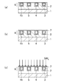
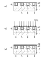
- FIGS. 12 (a) to 12 (c) show a method of manufacturing a semiconductor device for improving the adhesion between a conventional wiring and a surrounding film in order of steps. Yes.
- a first insulating film 102 is formed on a semiconductor substrate 101, and the first insulating film 102 is first formed on the first insulating film 102 by using a lithography method and a dry etching method.
- the wiring trench 103 is formed.
- the first barrier film 104 and the first copper (Cu) film are formed on the first insulating film 102 and on the side wall and the bottom surface of the first wiring groove 103.
- the first wiring trench 103 is embedded by sequentially forming 105.
- the first barrier film 104 and the first Cu film 105 formed outside the first wiring groove 103 are removed by a chemical mechanical polishing (CMP) method to form a lower wiring 106. To do.
- CMP chemical mechanical polishing
- the semiconductor substrate 101 is heated and exposed to a silicon compound such as SiH 4 , so that a copper silicide (CuSi) as a reaction layer is formed on the first Cu film 105. x )
- the layer 107 is formed.
- the upper surface of the CuSi x layer 107 is nitrided by exposing the top of the semiconductor substrate 101 to a plasma of a nitrogen compound such as ammonia (NH 3 ) to form silicon nitride ( SiN) layer 108 is formed.
- a nitrogen compound such as ammonia (NH 3 )
- a second insulating film 109 is formed so as to cover the first insulating film 102, the first barrier film 104, and the SiN film 108, and a lithography method and a dry etching method are performed.
- a via hole 110 exposing the lower wiring 106 is formed in the second insulating film 109.
- a plurality of second wiring trenches 111 are formed on the second insulating film 109.
- a part of the plurality of second wiring grooves 111 has a via hole 110 exposing the lower wiring 106.
- the second barrier film 112 is formed on the second insulating film 109, on the sidewall and bottom surface of the via hole 110, and on the sidewall and bottom surface of the second wiring trench 111. Then, the via hole 110 and the second wiring trench 111 are filled by sequentially forming the second Cu film 113. Subsequently, the second barrier film 112 and the second Cu film 113 formed outside the via hole 110 and the second wiring trench 111 are removed by CMP to form the upper wiring 114, thereby forming two layers. A semiconductor device including the wiring is completed. Thereafter, by repeating the steps shown in FIGS. 11C to 12C, a semiconductor device having a desired number of layers can be manufactured.
- the conventional method for manufacturing a semiconductor device has the following problems.
- an object of the present invention is to obtain a semiconductor device having practically sufficient electromigration resistance and operation speed.
- a method for manufacturing a semiconductor device has a structure in which a reaction layer is formed at the interface between a wiring and a protective film.
- the first method for manufacturing a semiconductor device includes a step (a) of forming a first insulating film on a semiconductor substrate, and a step of forming a wiring trench in the first insulating film ( b), a step (c) of forming a first wiring in the wiring trench, a step (d) of forming a protective film on the first insulating film and the first wiring, and a step (d) And (e) forming a reaction layer at the interface between the first wiring and the protective film.
- the protective film is formed on the first insulating film and the first wiring, and the reaction layer is formed at the interface between the first wiring and the protective film. Therefore, since the thickness of the reaction layer can be controlled with high accuracy, a semiconductor device having practically sufficient electromigration resistance and operation speed can be obtained.
- the step (e) is preferably performed by exposing the surface of the protective film to a silicon compound or a germanium compound.
- the step (e) preferably includes a step of chemically activating the reactive gas.
- step (e) it is preferable to chemically activate the reactive gas by ionizing.
- the step (e) preferably includes a step of physically activating the reactive gas.
- step (e) it is preferable to physically activate the reactive gas by imparting kinetic energy.
- the first method for manufacturing a semiconductor device includes a step (f) of forming a second insulating film on the protective film, and a step (g) of forming a via hole inside the second insulating film. And a step (h) of forming a second wiring so as to be connected to the via hole.
- the protective film is preferably a silicon carbonitride film.
- the manufacturing method of the first semiconductor device according to the present invention further includes a step (c1) of forming a coating layer on the first wiring between the step (c) and the step (d). Is preferred.
- the main constituent material of the coating layer is preferably any one of nickel, nickel alloy, cobalt and cobalt alloy.
- the first method for manufacturing a semiconductor device according to the present invention preferably further includes a step (e1) of exposing the surface of the protective film to plasma after the step (e).
- the plasma is preferably generated in an atmosphere containing a nitrogen compound.
- the first method for manufacturing a semiconductor device according to the present invention preferably further includes a step (e2) of exposing the surface of the protective film to ultraviolet light after the step (e).
- the first method for manufacturing a semiconductor device according to the present invention preferably further includes a step (e3) of forming a stopper film on the protective film after the step (e).
- the stopper film is preferably an oxygen-added silicon carbide film or a silicon nitride film.
- the reaction layer is preferably a silicon compound layer or a germanium compound layer.
- the main constituent material of the first wiring is any one of aluminum, aluminum alloy, copper, copper alloy, silver, silver alloy, gold, and gold alloy. It is preferable.
- a second method for manufacturing a semiconductor device includes a step of forming a first insulating film on a semiconductor substrate, a step of forming a wiring trench in the first insulating film, and a first step in the wiring trench.
- the method includes a step of forming a wiring and a step of forming a reaction layer on an upper portion of the first wiring, and the reaction layer is formed under a supply rate-limiting condition.
- the second method for manufacturing a semiconductor device of the present invention since the reaction layer is formed under the supply rate-determining condition, the thickness of the reaction layer can be accurately controlled. A semiconductor device having migration resistance and operation speed can be obtained.
- the reaction layer is preferably a silicon compound layer or a germanium compound layer.
- a semiconductor device includes a first insulating film formed on a semiconductor substrate, a first wiring formed on the first insulating film, and on the first insulating film and the first wiring. And a reaction layer formed at the interface between the first wiring and the protective film.
- the semiconductor device includes the first insulating film and the protective film formed on the first wiring, and the reaction layer formed at the interface between the first wiring and the protective film. Therefore, it becomes possible to control the thickness of the reaction layer with high accuracy, so that it is possible to obtain practically sufficient electromigration resistance and operation speed.
- a semiconductor device includes a second insulating film formed on the protective film, a via hole formed on the first wiring so as to penetrate the protective film and the second insulating film, A second wiring formed so as to be connected to the via hole may be further provided.
- the semiconductor device includes a stopper film formed on the protective film, a second insulating film formed on the stopper film, and a protective film, a stopper film, and a first film on the first wiring. It is preferable to further include a via hole formed so as to penetrate the two insulating films and a second wiring formed so as to be connected to the via hole.
- the protective film is preferably a silicon carbonitride film.
- the stopper film is preferably an oxygen-added silicon carbide film or a silicon nitride film.
- the reaction layer is preferably a silicon compound layer or a germanium compound layer.
- the reaction layer preferably contains nickel or cobalt.
- the main constituent material of the first wiring is preferably any one of aluminum, aluminum alloy, copper, copper alloy, silver, silver alloy, gold and gold alloy.
- the thickness of the reaction layer can be controlled with high accuracy, so that a semiconductor device having practically sufficient electromigration resistance and operation speed can be obtained.
- FIG. 1 is a cross-sectional view showing a semiconductor device according to the first embodiment of the present invention.
- 2A to 2D are cross-sectional views showing the method of manufacturing the semiconductor device according to the first embodiment of the present invention in the order of steps.
- 3A to 3C are cross-sectional views showing the method of manufacturing the semiconductor device according to the first embodiment of the present invention in the order of steps.
- FIG. 4 is a cross-sectional view showing a semiconductor device according to a first modification of the first embodiment of the present invention.
- FIG. 5A to FIG. 5C are cross-sectional views showing a method of manufacturing a semiconductor device according to the first modification of the first embodiment of the present invention in the order of steps.
- FIG. 6A to 6C are cross-sectional views showing a method of manufacturing a semiconductor device according to a first modification of the first embodiment of the present invention in the order of steps.
- FIG. 7A to FIG. 7D are cross-sectional views showing a method of manufacturing a semiconductor device according to a second modification of the first embodiment of the present invention in the order of steps.
- FIG. 8 is a sectional view showing a semiconductor device according to the second embodiment of the present invention.
- FIG. 9A to FIG. 9C are cross-sectional views showing a method of manufacturing a semiconductor device according to the second embodiment of the present invention in the order of steps.
- FIG. 10A to FIG. 10C are cross-sectional views showing a method of manufacturing a semiconductor device according to the second embodiment of the present invention in the order of steps.
- 11A to 11D are cross-sectional views showing a conventional method of manufacturing a semiconductor device in the order of steps.
- 12 (a) to 12 (c) are cross-sectional views showing a conventional method of manufacturing
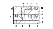
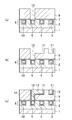
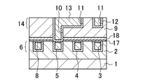
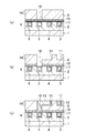
- a first insulating film 2 which is a carbon-added silicon oxide film (SiOC film), is formed on a semiconductor substrate 1, and the first insulating film 2 has a first insulating film 2 on the first insulating film 2.
- a wiring groove 3 is formed.
- a first barrier film 4 is formed on the side wall and the bottom surface of the first wiring groove 3, and the first copper film is embedded on the first barrier film 4 so as to bury the first wiring groove 3.
- a (Cu) film 5 is formed, and a lower wiring 6 is formed.
- a copper silicide (CuSi x ) layer 8 as a reaction layer is formed on the first Cu film 5 so as to cover the first insulating film 2, the first barrier film 4 and the CuSi x layer 8.
- a protective film 7 which is a silicon carbonitride film (SiCN film) having a thickness of about 10 nm is formed.
- a second insulating film 9 that is a SiOC film is formed on the protective film 7.
- a via hole 10 that penetrates the second insulating film 9 and the protective film 7 and exposes the lower wiring 6 is formed on a part of the CuSi x layer 8 and the first barrier film 4 formed in the periphery thereof.
- a plurality of second wiring trenches 11 are formed on the second insulating film 9. Some of the plurality of second wiring grooves 11 have via holes 10 exposing the lower wiring 6.
- a second barrier film 12 is formed on the side walls and the bottom surface of the via hole 10 and the second wiring groove 11, and the via hole 10 and the second wiring groove 11 are embedded on the second barrier film 12.
- the second Cu film 13 is formed, and the via and the upper wiring 14 are formed.
- vias connect the lower wiring 6 and the upper wiring 14.
- the semiconductor device includes a reaction layer having a thickness necessary for suppressing an increase in wiring resistance and improving adhesion between the wiring and a surrounding film. Therefore, practically sufficient electromigration resistance and operation speed can be obtained.
- a first insulating film 2 which is a SiOC film is formed on a semiconductor substrate 1, and the first insulating film 2 is formed on the first insulating film 2 by lithography and dry etching. 1 wiring groove 3 is formed.
- the first barrier film 4 and the first Cu film 5 are sequentially formed on the first insulating film 2 and on the side wall and the bottom surface of the first wiring groove 3. By forming, the first wiring groove 3 is embedded. Subsequently, the first barrier film 4 and the first Cu film 5 formed outside the first wiring trench 3 are removed by a chemical mechanical polishing (CMP) method to form the lower wiring 6.
- CMP chemical mechanical polishing
- the minimum line width of the lower wiring 6 is set to about 60 nm and the height is set to about 100 nm.
- the protective film 7 is a SiCN film having a thickness of about 10 nm so as to cover the first insulating film 2, the first barrier film 4 and the first Cu film 5. Form.
- the semiconductor substrate 1 is heated to about 400 ° C. and exposed to SiH 4 .
- a CuSi x layer 8 as a reaction layer is formed at the interface between the first Cu film 5 and the protective film 7. This is because SiH 4 diffuses inside the protective film 7, reaches the surface of the first Cu film 5, and reacts with the first Cu film 5.
- SiH 4 diffuses inside the protective film 7, reaches the surface of the first Cu film 5, and reacts with the first Cu film 5.
- a second insulating film 9 which is a SiOC film is formed on the protective film 7, and the protective film is formed on the second insulating film 9 by lithography and dry etching.
- a via hole 10 exposing 7 is formed.
- a plurality of second wiring grooves 11 are formed on the second insulating film 9 by lithography and dry etching, and a protective film on the bottom surface of the via hole 10 is formed. 7 is removed to expose the first barrier film 4 and the CuSi x layer 8. A part of the plurality of second wiring grooves 11 has a via hole 10 exposing the lower wiring 6.
- the second barrier film 12 is formed on the second insulating film 9, on the sidewall and bottom surface of the via hole 10, and on the sidewall and bottom surface of the second wiring groove 11.
- the second Cu film 13 is sequentially formed to fill the via hole 10 and the second wiring groove 11.
- the second barrier film 12 and the second Cu film 13 outside the via hole 10 and the second wiring groove 11 are removed by CMP to form a via and an upper wiring 14, thereby forming a two-layer wiring.
- the minimum line width of the upper wiring 14 is set to about 60 nm and the height is set to about 100 nm. Note that a semiconductor device having a desired number of wirings can be manufactured by repeating the steps shown in FIGS. 2C to 3C after the step shown in FIG.
- the method for manufacturing a semiconductor device according to the first embodiment of the present invention since the thickness of the CuSi x layer as a reaction layer can be accurately controlled, a semiconductor device having practically sufficient electromigration resistance and operation speed is obtained. Obtainable.
- the reason why the thickness of the CuSi x layer 8 can be accurately controlled as compared with the conventional technique will be described.
- SiH 4 is decomposed by a catalytic action on the surface of the Cu film to form a CuSi x layer. Since this reaction is reaction-limited at a low temperature of 300 ° C. or lower, the thickness of the formed CuSi x layer is greatly influenced by the surface temperature and crystal state of the Cu film.
- SiH 4 is diffused into the protective film 7 and supplied to the surface of the first Cu film 5. The reaction can be rate limited to supply of SiH 4 .
- the thickness of the CuSi x layer 8 to be formed is determined by the amount of SiH 4 reaching the surface of the first Cu film 5, it is not affected by the surface temperature and crystal state of the first Cu film 5.
- the thickness of the CuSi x layer 8 can be controlled with higher accuracy than in the conventional technique.
- the heating temperature of the semiconductor substrate 1 is set high, for example, to about 350 ° C.
- the partial pressure of SiH 4 is , for example, about 1 mPa
- the growth rate of the CuSi x layer 8 is high, and it is difficult to form the CuSi x layer 8 having a thickness of several nanometers necessary for manufacturing a semiconductor device with good controllability.
- a method of supplying SiH 4 through the protective film 7 is preferable.
- the protective film 7 since the role of the protective film 7 is to appropriately control the amount of SiH 4 reaching the surface of the first Cu film 5, the protective film 7 has a diameter that allows SiH 4 to pass therethrough. It is necessary to have the pores. Further, the protective film 7 is chemically inactive with respect to the first insulating film 2, the first Cu film 5, and the second insulating film 9, and needs to have appropriate adhesion.
- An example of a material that satisfies these requirements is SiCN containing CH 3 groups as impurities.
- Such a protective film 7 made of SiCN can be obtained by a plasma chemical vapor deposition (CVD) method using tetramethylsilane (TMS) and ammonia (NH 3 ) as source gases.
- the thickness of the protective film 7 is thinner than 2.5 nm, the frequency of abnormal growth of the CuSi x layer 8 due to pinholes or the like increases.
- the protective film 7 is thicker than 20 nm, the amount of SiH 4 reaching the surface of the first Cu film 5 is extremely reduced, and the growth rate of the CuSi x layer 8 is extremely reduced. End up. Therefore, the thickness of the protective film 7 is preferably set to about 2.5 nm or more and 20 nm or less. Therefore, in this embodiment, a SiCN film having a thickness of about 10 nm is used as the protective film 7.
- a preferable heating temperature of the semiconductor substrate 1 in the step shown in FIG. If the heating temperature is set lower than 300 ° C., the rate at which SiH 4 diffuses inside the protective film 7 decreases, and therefore a sufficiently thick CuSi x layer 8 cannot be obtained.
- the heating temperature is set higher than 400 ° C., a Si layer is formed on the surface of the protective film 7 due to the decomposition reaction of SiH 4 .
- the heating temperature is preferably set to about 300 ° C. or more and about 400 ° C. or less, and therefore, in this embodiment, the heating temperature is set to about 400 ° C.
- the thickness of the CuSi x layer 8 is preferably set to about 2 nm or more and 10 nm or less.
- the reaction layer 16 is formed on the first Cu film 5 and the protective film 7 is formed on the reaction layer 16, which is different from the first embodiment.
- the reaction layer 16 is made of a mixture of CuSi x and NiSi x .
- the adhesion between the first Cu film 5 and the protective film 7 is further improved as compared with the first embodiment, so that the electromigration resistance is further improved. Can do.
- the thickness necessary for suppressing the increase in the resistance of the wiring and improving the adhesion between the wiring and the surrounding film is increased. Since the reaction layer is provided, practically sufficient electromigration resistance and operation speed can be obtained.
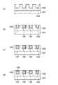
- FIGS. 5A to 5C and FIGS. 6A to 6C While explaining. 5A to FIG. 5C and FIG. 6A to FIG. 6C, FIG. 2A to FIG. 2D and FIG. 3A in the first embodiment.
- the same members as those shown in FIG. 3C are denoted by the same reference numerals, and description thereof is omitted.
- the steps from the formation of the semiconductor substrate 1 to the lower wiring 6 are the same as those in the first embodiment, and the description thereof is omitted.
- a coating layer 15 is formed on the first Cu film 5.
- the coating layer 15 needs to be selectively formed on the surface of the first Cu film 5 and must react with SiH 4 to generate a stable compound.
- Known materials that satisfy these requirements include nickel (Ni) films, Ni alloy films, cobalt (Co) films, and Co alloy films. These can be selectively formed on the surface of the first Cu film 5 by electroless plating.
- the coating layer 15 is a Ni layer deposited by an electroless plating method.
- a protective film 7 is formed so as to cover the first insulating film 2, the first barrier film 4 and the coating layer 15.
- the semiconductor substrate 1 is heated and exposed to SiH 4 .
- the reaction layer 16 is formed at the interface between the first Cu film 5 and the protective film 7.
- the reaction layer 16 is made of a mixture of CuSi x and NiSi x .
- a second insulating film 9 is formed on the protective film 7, and the second insulating film 9 is formed.
- the second barrier film 12 and the second Cu film 13 are sequentially formed so as to fill the via hole 10 and the second wiring groove 11, and the via and the upper part are formed.
- a wiring 14 is formed. Note that a semiconductor device having a desired number of wirings can be manufactured by repeating the steps shown in FIGS. 5B to 6C after the step shown in FIG. 6C.
- the thickness of the layer made of a mixture of CuSi x and NiSi x as the reaction layer can be controlled with high accuracy, so that electromigration resistance sufficient for practical use is achieved.
- a semiconductor device having an operation speed can be obtained.
- the surface of the protective film 7 is exposed to NH 3 plasma.
- the surface of the protective film 7 is in an atmosphere containing nitrogen compounds such as nitrogen (N 2 ), diazene (HN ⁇ NH) and hydrazine (H 2 N—NH 2 ). It is preferable to irradiate the plasma generated in step (b).
- Another preferred method is to irradiate the surface of the protective film 7 with ultraviolet light.
- a second insulating film 9 is formed on the protective film 7, and the second insulating film 9 is formed.
- the second barrier film 12 and the second Cu film 13 are sequentially formed so as to fill the via hole 10 and the second wiring groove 11, and the via and the upper part are formed.
- a wiring 14 is formed.
- the steps shown in FIGS. 2 (c), 2 (d) and 7 (a) to 7 (d) are repeated, so that a wiring having a desired number of layers can be obtained. It is also possible to manufacture a semiconductor device having
- This embodiment is an example in which a process is added to the first embodiment, but can be similarly applied to the first modification of the first embodiment.
- the thickness of the CuSi x layer that is the reaction layer can be controlled with high accuracy, a semiconductor device having practically sufficient electromigration resistance and operation speed can be obtained. Obtainable.
- a semiconductor device according to the second embodiment of the present invention will be described below with reference to FIG.
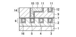
- the semiconductor device of the second embodiment is the same as the structure of the semiconductor substrate 1 to the lower wiring 6 and the CuSi x layer 8 shown in FIG.
- a protective film 17 that is a silicon carbonitride film (SiCN) having a thickness of about 5 nm is formed so as to cover the first insulating film 2, the first barrier film 4, and the CuSi x layer 8.
- a second insulating film 9 which is a SiOC film is formed. A part of the CuSi x layer 8 and the first barrier film 4 formed therearound penetrate the second insulating film 9, the stopper film 18 and the protective film 17, and pass through the CuSi x layer 8 and the first barrier film 4.
- a via hole 10 exposing the first barrier film 4 is formed, and a second wiring trench 11 is formed on the second insulating film 9.
- a second barrier film 12 is formed on the side walls and the bottom surface of the via hole 10 and the second wiring groove 11, and the via hole 10 and the second wiring groove 11 are embedded on the second barrier film 12.
- the second Cu film 13 is formed, and the via and the upper wiring 14 are formed.
- vias connect the lower wiring 6 and the upper wiring 14.
- the stopper film 18 having a large etching selection ratio with respect to the second insulating film 9 is formed.
- the semiconductor device includes a reaction layer having a thickness necessary for suppressing an increase in wiring resistance and improving adhesion between the wiring and a surrounding film. Therefore, practically sufficient electromigration resistance and operation speed can be obtained.
- FIGS. 9A to 9C and FIGS. 10A to 10C a method for manufacturing a semiconductor device according to the second embodiment of the present invention will be described with reference to FIGS. 9A to 9C and FIGS. 10A to 10C. 9A to FIG. 9C and FIG. 10A to FIG. 10C, FIG. 2A to FIG. 2D and FIG. 3A in the first embodiment.
- the same members as those shown in FIG. 3C are denoted by the same reference numerals, and description thereof is omitted.
- the steps from the formation of the semiconductor substrate 1 to the lower wiring 6 are the same as those in the first embodiment, and the description thereof is omitted.
- a protective film 17 which is a SiCN film having a film thickness of about 5 nm is formed on the first insulating film 2, the first barrier film 4 and the first Cu film 5. Form.
- a stopper film 18 is formed on the protective film 17.
- SiCO silicon nitride
- SiN silicon nitride
- SiCO can be obtained by a plasma CVD method using tetramethylsilane (TMS) and carbon dioxide (CO 2 ) as source gases
- SiN can be obtained by a plasma CVD method using silane and NH 3 as source gases.
- the stopper film 18 is a SiCO film having a thickness of about 20 nm.
- a second insulating film 9 is formed on the stopper film 18.
- a via hole 10 is formed inside the second insulating film 9.
- the etching of the via hole 10 is performed on the condition that the stopper film 18 has a lower etching rate than the second insulating film 9, and the etching is stopped on the surface of the stopper film 18.
- the yield may be good.
- a stopper film 18 having a high etching selectivity is formed on the second insulating film 9 and etching for forming the via hole 10 is performed until the stopper film 18 is exposed. Is effective.
- a plurality of second wiring grooves 11 are formed on the second insulating film 9, and the protective film 17 and the stopper film 18 at the bottom of the via hole 10 are removed.
- a second barrier film 12 and a second Cu film 13 are sequentially formed so as to fill the via hole 10 and the second wiring trench 11, and a via and an upper wiring 14 are formed.
- the steps shown in FIG. 9A to FIG. 9C and FIG. 10A to FIG. It is also possible to manufacture a semiconductor device having
- the present embodiment is an example in which a step of forming the stopper film 18 is added to the first embodiment, but the present embodiment is also applicable to the first modification and the second modification of the first embodiment. it can.
- the thickness of the CuSi x layer as the reaction layer can be controlled with high accuracy, so that a semiconductor device having practically sufficient electromigration resistance and operating speed can be obtained. it can.
- SiH 4 is used to form the CuSi x layer 8 or the reaction layer 16, but a silicon compound such as polysilane (Si n H 2n + 2 ) can be used instead.
- germanium compounds such as germane (GeH 4 ) and polygermane (Ge n H 2n + 2 ) can be used instead.
- germanium copper (CuGe x) layer is formed instead of CuSi x layer, the reaction layer 16 becomes a mixture of YGE x and CuGe x.
- Y is either Ni or Co.
- the surface of the protective film 7 is exposed to a reactive gas such as SiH 4 in order to form the CuSi x layer 8 or the reaction layer 16, but the reactive gas is chemically or physically exposed.
- a reactive gas such as SiH 4
- the reactive gas is chemically or physically exposed.
- a means for activating examples include radicalization or ionization of a reactive gas by plasma inside or outside the reactor. Further, as an example of the latter, the application of kinetic energy to the reactive gas by applying an ion implantation technique can be given.
- the lower wiring 6 is formed using the first Cu film 5.
- the Cu alloy film, the aluminum (Al) film, the Al alloy film, the silver (Ag) film, and the Ag alloy film are used. It is also possible to form the lower wiring 6 using a gold (Au) film, an Au alloy film, or the like.
- Au gold
- an Au alloy film, or the like instead of the CuSi x layer, an XSi x layer is formed, and the reaction layer 16 becomes a mixture of YGe x and CuGe x .
- X is a main constituent element of the lower wiring
- Y is either Ni or Co.
- the via hole 10 is formed before the second wiring groove 11, but conversely, the second wiring groove 11 can be formed before the via hole 10. .
- the semiconductor device and the manufacturing method thereof according to the present invention can accurately control the thickness of the reaction layer, it is possible to obtain practically sufficient electromigration resistance and operation speed. This is useful for a semiconductor device having a wiring structure and a method for manufacturing the same.
- first barrier film 1 semiconductor substrate 2 first insulating film 3 and the first wiring groove 4 first barrier film 5 first copper (Cu) film 6 lower wiring 7 protective layer 8 copper silicide (CuSi x) layer (reaction layer) 9 Second insulating film 10 Via hole 11 Second wiring trench 12 Second barrier film 13 Second copper (Cu) film 14 Upper wiring 15 Covering layer 16 Reaction layer 17 Protective film 18 Stopper film
Landscapes
- Engineering & Computer Science (AREA)
- Physics & Mathematics (AREA)
- Condensed Matter Physics & Semiconductors (AREA)
- General Physics & Mathematics (AREA)
- Computer Hardware Design (AREA)
- Microelectronics & Electronic Packaging (AREA)
- Power Engineering (AREA)
- Manufacturing & Machinery (AREA)
- Plasma & Fusion (AREA)
- Internal Circuitry In Semiconductor Integrated Circuit Devices (AREA)
Priority Applications (1)
| Application Number | Priority Date | Filing Date | Title |
|---|---|---|---|
| US13/274,039 US8927416B2 (en) | 2009-06-22 | 2011-10-14 | Semiconductor device and method of manufacturing the same |
Applications Claiming Priority (2)
| Application Number | Priority Date | Filing Date | Title |
|---|---|---|---|
| JP2009-148054 | 2009-06-22 | ||
| JP2009148054A JP5230542B2 (ja) | 2009-06-22 | 2009-06-22 | 半導体装置の製造方法 |
Related Child Applications (1)
| Application Number | Title | Priority Date | Filing Date |
|---|---|---|---|
| US13/274,039 Continuation US8927416B2 (en) | 2009-06-22 | 2011-10-14 | Semiconductor device and method of manufacturing the same |
Publications (1)
| Publication Number | Publication Date |
|---|---|
| WO2010150430A1 true WO2010150430A1 (ja) | 2010-12-29 |
Family
ID=43386221
Family Applications (1)
| Application Number | Title | Priority Date | Filing Date |
|---|---|---|---|
| PCT/JP2010/000444 Ceased WO2010150430A1 (ja) | 2009-06-22 | 2010-01-27 | 半導体装置及びその製造方法 |
Country Status (3)
| Country | Link |
|---|---|
| US (1) | US8927416B2 (enExample) |
| JP (1) | JP5230542B2 (enExample) |
| WO (1) | WO2010150430A1 (enExample) |
Families Citing this family (6)
| Publication number | Priority date | Publication date | Assignee | Title |
|---|---|---|---|---|
| US20160276156A1 (en) * | 2015-03-16 | 2016-09-22 | Taiwan Semiconductor Manufacturing Company Ltd. | Semiconductor device and manufacturing process thereof |
| US9673091B2 (en) * | 2015-06-25 | 2017-06-06 | Globalfoundries Inc. | Structure for BEOL metal levels with multiple dielectric layers for improved dielectric to metal adhesion |
| DE102019131408B4 (de) | 2019-06-28 | 2025-12-04 | Taiwan Semiconductor Manufacturing Company, Ltd. | Verbesserte Kontaktierung von Metallleitungen bei Fehlausrichtung von BEOL-Durchkontaktierungen |
| CN112151497B (zh) * | 2019-06-28 | 2023-08-22 | 台湾积体电路制造股份有限公司 | 半导体结构以及形成半导体结构的方法 |
| US12272600B2 (en) * | 2022-01-12 | 2025-04-08 | Taiwan Semiconductor Manufacturing Co., Ltd. | Contact features of semiconductor device and method of forming same |
| CN115732405A (zh) * | 2022-09-20 | 2023-03-03 | 长鑫存储技术有限公司 | 半导体结构的形成方法及半导体结构 |
Citations (5)
| Publication number | Priority date | Publication date | Assignee | Title |
|---|---|---|---|---|
| JP2000058544A (ja) * | 1998-08-04 | 2000-02-25 | Matsushita Electron Corp | 半導体装置及びその製造方法 |
| JP2002246391A (ja) * | 2001-02-21 | 2002-08-30 | Nec Corp | 半導体装置の製造方法 |
| JP2004096052A (ja) * | 2002-03-13 | 2004-03-25 | Nec Electronics Corp | 半導体装置およびその製造方法ならびに金属配線 |
| JP2007027769A (ja) * | 2005-07-20 | 2007-02-01 | Samsung Electronics Co Ltd | 二重キャッピング膜を有する半導体素子の配線及びその形成方法 |
| JP2009016520A (ja) * | 2007-07-04 | 2009-01-22 | Tokyo Electron Ltd | 半導体装置の製造方法及び半導体装置の製造装置 |
Family Cites Families (4)
| Publication number | Priority date | Publication date | Assignee | Title |
|---|---|---|---|---|
| TW379387B (en) | 1996-11-29 | 2000-01-11 | Texas Instruments Inc | A process for encapsulation of copper surfaces |
| US6448655B1 (en) * | 1998-04-28 | 2002-09-10 | International Business Machines Corporation | Stabilization of fluorine-containing low-k dielectrics in a metal/insulator wiring structure by ultraviolet irradiation |
| US20050250346A1 (en) * | 2004-05-06 | 2005-11-10 | Applied Materials, Inc. | Process and apparatus for post deposition treatment of low k dielectric materials |
| JP2009016502A (ja) * | 2007-07-03 | 2009-01-22 | Tdk Corp | ワイヤ被膜剥離方法、コイル部品の製造方法、ワイヤ被膜剥離装置およびコイル部品の製造装置 |
-
2009
- 2009-06-22 JP JP2009148054A patent/JP5230542B2/ja not_active Expired - Fee Related
-
2010
- 2010-01-27 WO PCT/JP2010/000444 patent/WO2010150430A1/ja not_active Ceased
-
2011
- 2011-10-14 US US13/274,039 patent/US8927416B2/en active Active
Patent Citations (5)
| Publication number | Priority date | Publication date | Assignee | Title |
|---|---|---|---|---|
| JP2000058544A (ja) * | 1998-08-04 | 2000-02-25 | Matsushita Electron Corp | 半導体装置及びその製造方法 |
| JP2002246391A (ja) * | 2001-02-21 | 2002-08-30 | Nec Corp | 半導体装置の製造方法 |
| JP2004096052A (ja) * | 2002-03-13 | 2004-03-25 | Nec Electronics Corp | 半導体装置およびその製造方法ならびに金属配線 |
| JP2007027769A (ja) * | 2005-07-20 | 2007-02-01 | Samsung Electronics Co Ltd | 二重キャッピング膜を有する半導体素子の配線及びその形成方法 |
| JP2009016520A (ja) * | 2007-07-04 | 2009-01-22 | Tokyo Electron Ltd | 半導体装置の製造方法及び半導体装置の製造装置 |
Also Published As
| Publication number | Publication date |
|---|---|
| US8927416B2 (en) | 2015-01-06 |
| JP2011003859A (ja) | 2011-01-06 |
| JP5230542B2 (ja) | 2013-07-10 |
| US20120032333A1 (en) | 2012-02-09 |
Similar Documents
| Publication | Publication Date | Title |
|---|---|---|
| CN100355068C (zh) | 半导体器件及其制造方法 | |
| US8222135B2 (en) | Increasing reliability of copper-based metallization structures in a microstructure device by using aluminum nitride | |
| JP4674061B2 (ja) | 薄膜形成方法 | |
| JP5500810B2 (ja) | 多層配線構造に空隙を形成する方法 | |
| CN101286494B (zh) | 半导体结构及其制造方法 | |
| CN103996651B (zh) | 半导体器件及其制造方法 | |
| KR100719177B1 (ko) | 선택적 원자층 증착법을 이용한 텅스텐막 형성 방법 | |
| JP5230542B2 (ja) | 半導体装置の製造方法 | |
| CN101728319B (zh) | 通过硅/锗浸泡改进金属线的电路结构及其形成方法 | |
| CN105679651A (zh) | 内连线结构的形成方法 | |
| KR100602087B1 (ko) | 반도체 소자 및 그 제조방법 | |
| CN100583427C (zh) | 用于微电子元件的金属互连结构 | |
| KR101430832B1 (ko) | 낮은 접촉 저항 탄소 나노튜브 상호연결부를 위한 장치 및 방법 | |
| CN112435958A (zh) | 集成电路结构及其形成方法 | |
| JP5217272B2 (ja) | 配線の形成方法及び半導体装置の製造方法 | |
| CN110660729B (zh) | 半导体装置的形成方法 | |
| KR101152203B1 (ko) | 반도체 장치 및 그의 제조 방법 | |
| CN101304002A (zh) | 半导体元件的制造方法 | |
| JP2011029554A (ja) | 半導体装置の製造方法 | |
| US7902641B2 (en) | Semiconductor device and manufacturing method therefor | |
| JP2007157959A (ja) | 半導体装置の製造方法および半導体装置 | |
| JP2007258390A (ja) | 半導体装置、および半導体装置の製造方法 | |
| JP2010080606A (ja) | 半導体装置の製造方法 | |
| KR20060011396A (ko) | 반도체 소자의 다층 금속배선 형성방법 | |
| KR100571387B1 (ko) | 반도체 소자의 구리 배선 제조 방법 |
Legal Events
| Date | Code | Title | Description |
|---|---|---|---|
| 121 | Ep: the epo has been informed by wipo that ep was designated in this application |
Ref document number: 10791758 Country of ref document: EP Kind code of ref document: A1 |
|
| NENP | Non-entry into the national phase |
Ref country code: DE |
|
| 122 | Ep: pct application non-entry in european phase |
Ref document number: 10791758 Country of ref document: EP Kind code of ref document: A1 |