WO2010146987A1 - 画像表示装置、画像表示方法、及びプログラム - Google Patents
画像表示装置、画像表示方法、及びプログラム Download PDFInfo
- Publication number
- WO2010146987A1 WO2010146987A1 PCT/JP2010/059250 JP2010059250W WO2010146987A1 WO 2010146987 A1 WO2010146987 A1 WO 2010146987A1 JP 2010059250 W JP2010059250 W JP 2010059250W WO 2010146987 A1 WO2010146987 A1 WO 2010146987A1
- Authority
- WO
- WIPO (PCT)
- Prior art keywords
- frame rate
- video
- frame
- signal
- image display
- Prior art date
- Legal status (The legal status is an assumption and is not a legal conclusion. Google has not performed a legal analysis and makes no representation as to the accuracy of the status listed.)
- Ceased
Links
Images

Classifications
-
- H—ELECTRICITY
- H04—ELECTRIC COMMUNICATION TECHNIQUE
- H04N—PICTORIAL COMMUNICATION, e.g. TELEVISION
- H04N7/00—Television systems
- H04N7/01—Conversion of standards, e.g. involving analogue television standards or digital television standards processed at pixel level
- H04N7/0127—Conversion of standards, e.g. involving analogue television standards or digital television standards processed at pixel level by changing the field or frame frequency of the incoming video signal, e.g. frame rate converter
-
- G—PHYSICS
- G09—EDUCATION; CRYPTOGRAPHY; DISPLAY; ADVERTISING; SEALS
- G09G—ARRANGEMENTS OR CIRCUITS FOR CONTROL OF INDICATING DEVICES USING STATIC MEANS TO PRESENT VARIABLE INFORMATION
- G09G5/00—Control arrangements or circuits for visual indicators common to cathode-ray tube indicators and other visual indicators
- G09G5/003—Details of a display terminal, the details relating to the control arrangement of the display terminal and to the interfaces thereto
-
- G—PHYSICS
- G09—EDUCATION; CRYPTOGRAPHY; DISPLAY; ADVERTISING; SEALS
- G09G—ARRANGEMENTS OR CIRCUITS FOR CONTROL OF INDICATING DEVICES USING STATIC MEANS TO PRESENT VARIABLE INFORMATION
- G09G5/00—Control arrangements or circuits for visual indicators common to cathode-ray tube indicators and other visual indicators
- G09G5/36—Control arrangements or circuits for visual indicators common to cathode-ray tube indicators and other visual indicators characterised by the display of a graphic pattern, e.g. using an all-points-addressable [APA] memory
-
- H—ELECTRICITY
- H04—ELECTRIC COMMUNICATION TECHNIQUE
- H04N—PICTORIAL COMMUNICATION, e.g. TELEVISION
- H04N7/00—Television systems
- H04N7/01—Conversion of standards, e.g. involving analogue television standards or digital television standards processed at pixel level
- H04N7/0127—Conversion of standards, e.g. involving analogue television standards or digital television standards processed at pixel level by changing the field or frame frequency of the incoming video signal, e.g. frame rate converter
- H04N7/0132—Conversion of standards, e.g. involving analogue television standards or digital television standards processed at pixel level by changing the field or frame frequency of the incoming video signal, e.g. frame rate converter the field or frame frequency of the incoming video signal being multiplied by a positive integer, e.g. for flicker reduction
-
- G—PHYSICS
- G09—EDUCATION; CRYPTOGRAPHY; DISPLAY; ADVERTISING; SEALS
- G09G—ARRANGEMENTS OR CIRCUITS FOR CONTROL OF INDICATING DEVICES USING STATIC MEANS TO PRESENT VARIABLE INFORMATION
- G09G2310/00—Command of the display device
- G09G2310/06—Details of flat display driving waveforms
- G09G2310/061—Details of flat display driving waveforms for resetting or blanking
- G09G2310/063—Waveforms for resetting the whole screen at once
-
- G—PHYSICS
- G09—EDUCATION; CRYPTOGRAPHY; DISPLAY; ADVERTISING; SEALS
- G09G—ARRANGEMENTS OR CIRCUITS FOR CONTROL OF INDICATING DEVICES USING STATIC MEANS TO PRESENT VARIABLE INFORMATION
- G09G2320/00—Control of display operating conditions
- G09G2320/02—Improving the quality of display appearance
- G09G2320/0247—Flicker reduction other than flicker reduction circuits used for single beam cathode-ray tubes
-
- G—PHYSICS
- G09—EDUCATION; CRYPTOGRAPHY; DISPLAY; ADVERTISING; SEALS
- G09G—ARRANGEMENTS OR CIRCUITS FOR CONTROL OF INDICATING DEVICES USING STATIC MEANS TO PRESENT VARIABLE INFORMATION
- G09G2320/00—Control of display operating conditions
- G09G2320/02—Improving the quality of display appearance
- G09G2320/0252—Improving the response speed
-
- G—PHYSICS
- G09—EDUCATION; CRYPTOGRAPHY; DISPLAY; ADVERTISING; SEALS
- G09G—ARRANGEMENTS OR CIRCUITS FOR CONTROL OF INDICATING DEVICES USING STATIC MEANS TO PRESENT VARIABLE INFORMATION
- G09G2320/00—Control of display operating conditions
- G09G2320/02—Improving the quality of display appearance
- G09G2320/0257—Reduction of after-image effects
-
- G—PHYSICS
- G09—EDUCATION; CRYPTOGRAPHY; DISPLAY; ADVERTISING; SEALS
- G09G—ARRANGEMENTS OR CIRCUITS FOR CONTROL OF INDICATING DEVICES USING STATIC MEANS TO PRESENT VARIABLE INFORMATION
- G09G2340/00—Aspects of display data processing
- G09G2340/04—Changes in size, position or resolution of an image
- G09G2340/0407—Resolution change, inclusive of the use of different resolutions for different screen areas
- G09G2340/0435—Change or adaptation of the frame rate of the video stream
Definitions
- the present invention relates to an image display device, an image display method, and a program.
- the user may desire to display at a normal frame rate.
- the frame rate is returned to the normal frame rate by a method such as frame doubling that continuously displays the same frame without changing the frame rate
- the same image is continuously displayed, which causes a problem of deterioration of the image. is there.
- the viewer moves the line of sight by predicting the position next to the moving object, but the video stops at the same location, so the viewer This causes a problem that the image is recognized twice.
- the present invention has been made in view of the above problems, and an object of the present invention is to reliably suppress deterioration of video due to continuous display of video for each frame. Another object of the present invention is to provide a new and improved image display device, image display method, and program.
- a high frame rate signal generation unit that increases a frame rate of an input video signal, and a high frame rate image output from the high frame rate signal generation unit
- An image comprising: a frame rate adjusting unit that adjusts a frame rate by providing a non-light emitting frame with a predetermined period for a signal; and a display panel that displays an image based on a video signal output from the frame rate adjusting unit.
- a display device is provided.
- the frame rate adjusting unit may include a light emission control unit that extends the light emission time of the frame immediately before the non-light emitting frame to the field of the non-light emitting frame.
- the frame rate adjustment unit is configured to analyze a video synchronization signal of the high frame rate video signal generated by the high frame rate signal generation unit, and based on the analysis result of the video synchronization signal, And a control timing generation unit that deletes the video synchronization signal of the frame to be emitted.
- a step of increasing a frame rate of an input video signal, and a high frame rate video signal output from the high frame rate signal generation unit are provided.
- an image display method comprising: a step of adjusting a frame rate by providing a non-light emitting frame at a predetermined period; and a step of displaying a video based on a video signal output from the frame rate adjustment unit.
- a means for increasing a frame rate of an input video signal, a predetermined period for a video signal output from the high frame rate signal generator A program for causing a computer to function as means for adjusting a frame rate by providing a non-light emitting frame and means for displaying a video based on a video signal output from the frame rate adjustment unit is provided.
- the present invention it is possible to reliably suppress the deterioration of the video due to the video being continuously displayed for each frame.
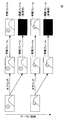
- FIG. 1 is a schematic diagram illustrating a schematic configuration of an image display device according to an embodiment of the present invention. It is a figure which shows typically the image
- a high frame rate video In the high frame rate video, more frames are displayed compared to the normal 60 frames (60 [Hz]) video, so that the user can enjoy a very smooth video.
- a high frame rate video is originally generated from a video signal of 60 [Hz], and creates a video that does not originally exist between 60 frames of video. For this reason, the quality of the video may be degraded.
- a television receiver or the like that is generally equipped with a video display function at a high frame rate has a mode for turning off the function.
- a normal high frame rate IC When turning off the video display function with a high frame rate, a normal high frame rate IC does not lower the frame rate to 60 [Hz], but outputs a frame-doubled video while maintaining the high frame rate. In this way, the off function is realized. In this case, the same video is displayed twice in succession.
- Frame doubling is effective for devices that are hold-type and have a slow response speed, such as liquid crystal displays.
- a self-luminous organic EL display or the like has a very fast response speed, there is a problem that when the frame-doubled image is displayed, the image appears double.
- the image display device 10 includes a high frame rate signal generation unit 20, a frame rate adjustment unit 30, and a display panel 40.
- FIG. 2 schematically shows a video for each frame with the vertical axis as a time axis.
- an image based on an input signal (60 [Hz]) to the high frame rate signal generation unit 20 an image based on an output signal (120 [Hz]) from the high frame rate signal generation unit 20, and a frame
- An image based on an output signal (120 [Hz]) from the rate adjusting unit 30 is schematically shown for each frame.
- the high frame rate signal generation unit 20 receives a video signal of 60 [Hz] such as a television signal.
- the high frame rate signal generation unit 20 doubles the video signal of 60 [Hz] to generate a high frame rate video signal of 120 [Hz].
- the high frame rate signal generation unit 20 generates (doubles) signals corresponding to two videos from a signal corresponding to one video.
- a high frame rate video signal in which the number of frames per unit time is doubled is generated. Note that the frequency of the high frame rate is not limited to this.
- the frame rate adjustment unit 30 adjusts the frame rate for the high frame rate video signal of 120 [Hz] generated by the high frame rate signal generation unit 20 when the video display function by the high frame rate is turned off. Perform the process.
- the signal is adjusted so that a frame for each frame is not emitted with respect to a high frame rate video signal of 120 [Hz].
- the display panel 40 is composed of a display panel such as an organic EL (OLED) display panel, for example, and pixels that perform light emission display are arranged in a matrix.
- the display panel 40 receives an input of the signal output from the frame rate adjustment unit 30 and causes each pixel to emit light based on the input signal.
- OLED organic EL
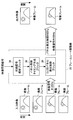
- FIG. 3 is a schematic diagram illustrating a configuration of the frame rate adjustment unit 30.
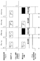
- FIG. 4 is a timing chart showing the operation of the image display apparatus 10.
- the frame rate adjustment unit 30 includes a synchronization signal analysis block 32, a panel control timing generation block 36, and an OLED panel light emission control block 38.
- Each component shown in FIGS. 1 and 3 is based on hardware (circuit) such as a high frame rate IC, or a central processing unit such as a CPU (Central Processing Unit) and a program (software) for causing it to function. Can be configured.
- a central processing unit such as a CPU (Central Processing Unit) and a program (software) for causing it to function.
- the program can be stored in a memory or the like provided in the image display device.
- the processing of the image display method according to the present embodiment is realized by a processing procedure sequentially performed by each component shown in FIGS. 1 and 3.
- FIG. 4 is a timing chart showing various signals and data related to the operation of the image processing apparatus 10.
- the “video synchronization signal (Vsync)” shown in FIG. 4 is generated in accordance with the display timing of each frame when the high frame rate video signal is generated by the high frame rate signal generator 20.
- the “video data” shown in FIG. 4 is video data corresponding to the high frame rate video signal output from the high frame rate signal generation unit 20.
- the “panel-video synchronization signal (P_Vsync)” shown in FIG. 4 is a video synchronization signal after the even-frame video synchronization signal is deleted in the panel control timing generation block 36 described later.
- “video to be displayed” shown in FIG. 4 indicates video that is actually displayed on the display panel 40.
- a “panel light emission control signal (Emit-Ctrl)” shown in FIG. 4 indicates a signal for controlling the light emission time of a frame displayed on the display panel 40.
- a high frame rate video signal is input from the high frame rate signal generation unit 20 to the OLED panel light emission control block 38.
- the synchronization signal analysis block 32 receives a video synchronization signal (a signal for synchronizing each frame) from the high frame rate signal generation unit 20.
- One pulse of the video synchronization signal is a pulse indicating the start of one predetermined frame.
- the frequency of the video synchronization signal is 120 [Hz], which is twice the normal frequency (60 [Hz] which is the frame rate). Accordingly, a pulse indicating the start of the same frame is output twice in succession during the normal frame rate of 60 [Hz].
- the synchronization signal analysis block 32 analyzes whether or not the current frame is a frame providing a non-light emission period based on the video synchronization signal input from the high frame rate signal generation unit 20. In the present embodiment, as shown in FIG. 4, a non-light emission time is provided for even frames. Therefore, the synchronization signal analysis block 32 analyzes whether the current frame is an even frame or an odd frame based on the video synchronization signal, and outputs the analysis result to the panel control timing generation block 36.
- the panel control timing generation block 36 performs processing for deleting the video synchronization signal (Vsync) for a frame in which a non-light emission period is provided based on the analysis result of the synchronization signal analysis block 32.
- the video synchronization signal (Vsync) of the even frame is deleted.
- the panel-video synchronization signal (P_Vsync) shown in FIG. 4 is obtained.
- the panel-video synchronization signal (P_Vsync) is a signal indicating the timing at which the video of the corresponding frame is displayed on the display panel 40, the even-frame video is not displayed by deleting the even-frame synchronization signal. Become. Therefore, the even frame is a non-light emitting period.
- the OLED panel light emission control block 38 determines the light emission period in the odd-numbered frame.
- the light emission period of the odd-numbered frame is a section in which the panel light emission control signal (Emit-Ctrl) shown in FIG. 4 is high, and the OLED panel light emission control block 38 determines the duty ratio of the panel light emission control signal (Emit-Ctrl). .
- the OLED panel light emission control block 38 sets the duty ratio of the panel light emission control signal (Emit-Ctrl) so that the light emission period in the odd frame overlaps the field of the light emission period in the original even frame. . More specifically, in a state where the video synchronization signal is not deleted, light emission of the even frame starts at the timing when the video synchronization signal becomes high (t2 and t5 shown in FIG. 4). The end is set at a timing after the times t2 and t5. As described above, the light emission period of the odd frame is extended to the field of the light emission period of the even frame before the video synchronization signal is deleted.
- the video signal 120 [Hz]
- the OLED panel light emission control block 38 in a state where the video synchronization signal of the even frame is deleted (panel-video synchronization signal (P_Vsync) shown in FIG. 4).
- a panel light emission control signal (Emit-Ctrl) is output.
- the video signal is 120 [Hz]
- the panel light emission control signal has a period of 60 [Hz] in order to control the light emission time of an odd frame image.
- the even-frame video is not emitted and is not displayed on the display panel 40 by deleting the even-frame video synchronization signal. For this reason, compared with the off function of high frame rate video display by frame doubling, even in an organic EL display or the like having a particularly high response speed, the video does not appear double. Therefore, it is possible to display a good video image without deterioration when the high frame rate video display function is off.
- the light emission time of the odd frame is extended to the field of the even frame where no display is performed. Thereby, even when the even frame is not displayed, it is possible to reliably compensate for the decrease in luminance.
- the extension of the light emission period of the frame is, for example, about 40% of the period of the field of the even frame (between t2 and t4).
- the end of the light emission period in the odd frame may be set before the start times t2 and t5 of the field in the even frame. Even in this case, by bringing the end of the light emission period closer to the times t2 and t5, it is possible to extend the light emission period as compared with the normal odd frame light emission period, and it is possible to suppress the deterioration of the image and the decrease in luminance. It becomes.
- the high frame rate off function is provided without degrading the video by providing a frame that does not display the video. It can be realized. Further, by extending the light emission period of the frame for displaying the video to the section of the frame for not displaying the video, it is possible to reliably compensate for the decrease in luminance due to the provision of the frame for not displaying the video.
Landscapes
- Engineering & Computer Science (AREA)
- Multimedia (AREA)
- Signal Processing (AREA)
- Physics & Mathematics (AREA)
- Computer Hardware Design (AREA)
- General Physics & Mathematics (AREA)
- Theoretical Computer Science (AREA)
- Control Of Indicators Other Than Cathode Ray Tubes (AREA)
- Electroluminescent Light Sources (AREA)
- Control Of El Displays (AREA)
- Controls And Circuits For Display Device (AREA)
- Transforming Electric Information Into Light Information (AREA)
Priority Applications (4)
| Application Number | Priority Date | Filing Date | Title |
|---|---|---|---|
| EP10789362A EP2444960A4 (en) | 2009-06-16 | 2010-06-01 | PICTURE DISPLAY, PICTURE DISPLAY PROGRAM AND PROGRAM |
| US13/256,972 US8743279B2 (en) | 2009-06-16 | 2010-06-01 | Image display device, image display method, and program |
| CN201080025295.8A CN102804257B (zh) | 2009-06-16 | 2010-06-01 | 图像显示装置和图像显示方法 |
| US14/264,714 US9197847B2 (en) | 2009-06-16 | 2014-04-29 | Image display device, image display method, and program |
Applications Claiming Priority (2)
| Application Number | Priority Date | Filing Date | Title |
|---|---|---|---|
| JP2009-143726 | 2009-06-16 | ||
| JP2009143726A JP5321269B2 (ja) | 2009-06-16 | 2009-06-16 | 画像表示装置、画像表示方法、及びプログラム |
Related Child Applications (2)
| Application Number | Title | Priority Date | Filing Date |
|---|---|---|---|
| US13/256,972 A-371-Of-International US8743279B2 (en) | 2009-06-16 | 2010-06-01 | Image display device, image display method, and program |
| US14/264,714 Continuation US9197847B2 (en) | 2009-06-16 | 2014-04-29 | Image display device, image display method, and program |
Publications (1)
| Publication Number | Publication Date |
|---|---|
| WO2010146987A1 true WO2010146987A1 (ja) | 2010-12-23 |
Family
ID=43356307
Family Applications (1)
| Application Number | Title | Priority Date | Filing Date |
|---|---|---|---|
| PCT/JP2010/059250 Ceased WO2010146987A1 (ja) | 2009-06-16 | 2010-06-01 | 画像表示装置、画像表示方法、及びプログラム |
Country Status (7)
| Country | Link |
|---|---|
| US (2) | US8743279B2 (enExample) |
| EP (1) | EP2444960A4 (enExample) |
| JP (1) | JP5321269B2 (enExample) |
| KR (1) | KR20120032466A (enExample) |
| CN (1) | CN102804257B (enExample) |
| TW (1) | TWI419143B (enExample) |
| WO (1) | WO2010146987A1 (enExample) |
Families Citing this family (3)
| Publication number | Priority date | Publication date | Assignee | Title |
|---|---|---|---|---|
| JP2013026727A (ja) | 2011-07-19 | 2013-02-04 | Sony Corp | 表示装置および表示方法 |
| US11468809B2 (en) * | 2015-01-07 | 2022-10-11 | Apple Inc. | Low-flicker variable refresh rate display |
| JP6368727B2 (ja) * | 2016-02-17 | 2018-08-01 | サターン ライセンシング エルエルシーSaturn Licensing LLC | 表示装置および表示方法 |
Citations (8)
| Publication number | Priority date | Publication date | Assignee | Title |
|---|---|---|---|---|
| JP2002006818A (ja) * | 2000-06-23 | 2002-01-11 | Toshiba Corp | 画像処理装置および方法ならびに画像表示システム |
| JP2002215111A (ja) * | 2001-01-18 | 2002-07-31 | Matsushita Electric Ind Co Ltd | 映像表示装置 |
| JP2004233932A (ja) * | 2003-02-03 | 2004-08-19 | Sharp Corp | 液晶表示装置 |
| JP2004253827A (ja) * | 2002-12-25 | 2004-09-09 | Sharp Corp | 液晶表示装置 |
| JP2007133051A (ja) * | 2005-11-09 | 2007-05-31 | Hitachi Displays Ltd | 画像表示装置 |
| JP2007316293A (ja) * | 2006-05-25 | 2007-12-06 | Hitachi Displays Ltd | 画像表示装置、及び画像表示方法 |
| JP2009058785A (ja) * | 2007-08-31 | 2009-03-19 | Sony Corp | 投射型表示装置および投射表示制御プログラム |
| JP2009300785A (ja) * | 2008-06-13 | 2009-12-24 | Canon Inc | 表示装置及びその駆動方法 |
Family Cites Families (28)
| Publication number | Priority date | Publication date | Assignee | Title |
|---|---|---|---|---|
| US5844617A (en) * | 1995-10-05 | 1998-12-01 | Yves C. Faroudja | Method and apparatus for enhancing the vertical resolution of a television signal having degraded vertical chrominance transitions |
| JP3472667B2 (ja) * | 1996-08-30 | 2003-12-02 | 株式会社日立製作所 | ビデオデータ処理装置およびビデオデータ表示装置 |
| US6380985B1 (en) * | 1998-09-14 | 2002-04-30 | Webtv Networks, Inc. | Resizing and anti-flicker filtering in reduced-size video images |
| JP2002221935A (ja) * | 2000-11-24 | 2002-08-09 | Mitsubishi Electric Corp | 表示装置 |
| JP2003280600A (ja) | 2002-03-20 | 2003-10-02 | Hitachi Ltd | 表示装置およびその駆動方法 |
| JP2005191933A (ja) * | 2003-12-25 | 2005-07-14 | Funai Electric Co Ltd | 送信装置、送受信システム |
| KR100620519B1 (ko) * | 2004-02-16 | 2006-09-13 | 비오이 하이디스 테크놀로지 주식회사 | 비월 방식 비디오 신호 보상 방법 및 장치 |
| JP4337673B2 (ja) * | 2004-07-21 | 2009-09-30 | ソニー株式会社 | 表示装置および方法、記録媒体、並びにプログラム |
| US7259779B2 (en) * | 2004-08-13 | 2007-08-21 | Microsoft Corporation | Automatic assessment of de-interlaced video quality |
| US20060044241A1 (en) * | 2004-08-31 | 2006-03-02 | Vast View Technology Inc. | Driving device for quickly changing the gray level of the liquid crystal display and its driving method |
| US7839454B2 (en) * | 2004-12-13 | 2010-11-23 | Broadcom Corporation | Post-processor design supporting non-flickering interlaced display |
| JP4569388B2 (ja) * | 2005-05-31 | 2010-10-27 | 日本ビクター株式会社 | 画像表示装置 |
| EP1931141A4 (en) * | 2005-09-30 | 2010-11-03 | Sharp Kk | IMAGE DISPLAY DEVICE AND METHOD |
| CN100498911C (zh) * | 2005-10-14 | 2009-06-10 | 群康科技(深圳)有限公司 | 液晶显示装置的驱动方法 |
| JP4131281B2 (ja) * | 2006-05-09 | 2008-08-13 | ソニー株式会社 | 画像表示装置、信号処理装置、および画像処理方法、並びにコンピュータ・プログラム |
| JP4232790B2 (ja) * | 2006-05-09 | 2009-03-04 | ソニー株式会社 | 画像表示装置、制御信号生成装置、および画像表示制御方法、並びにコンピュータ・プログラム |
| JP2008003519A (ja) * | 2006-06-26 | 2008-01-10 | Toshiba Corp | 液晶受像装置 |
| TW200805225A (en) * | 2006-07-12 | 2008-01-16 | Chi Mei Optoelectronics Corp | LCD monitor and method for inserting black frame |
| US7656374B2 (en) * | 2006-09-04 | 2010-02-02 | Vastview Technology, Inc. | Method for enhancing response speed of hold-typed display device |
| JP4181593B2 (ja) * | 2006-09-20 | 2008-11-19 | シャープ株式会社 | 画像表示装置及び方法 |
| US8284318B2 (en) * | 2006-11-07 | 2012-10-09 | Seiko Epson Corporation | Image processing apparatus, image processing method, electro-optical device and electronic device |
| US20080231579A1 (en) * | 2007-03-22 | 2008-09-25 | Max Vasquez | Motion blur mitigation for liquid crystal displays |
| US8736535B2 (en) * | 2007-03-29 | 2014-05-27 | Nlt Technologies, Ltd. | Hold type image display system |
| JP5050691B2 (ja) * | 2007-07-05 | 2012-10-17 | ソニー株式会社 | 画像処理装置、画像処理方法およびコンピュータプログラム |
| US7897971B2 (en) * | 2007-07-26 | 2011-03-01 | Semiconductor Energy Laboratory Co., Ltd. | Display device |
| US20090179833A1 (en) * | 2008-01-15 | 2009-07-16 | Semiconductor Energy Laboratory Co., Ltd. | Display device and electronic appliance |
| US8059200B2 (en) * | 2008-04-14 | 2011-11-15 | National Semiconductor Corporation | Video clock generator for multiple video formats |
| JP2010286587A (ja) | 2009-06-10 | 2010-12-24 | Sony Corp | 画像表示装置、画像表示観察システム、画像表示方法、及びプログラム |
-
2009
- 2009-06-16 JP JP2009143726A patent/JP5321269B2/ja active Active
-
2010
- 2010-06-01 WO PCT/JP2010/059250 patent/WO2010146987A1/ja not_active Ceased
- 2010-06-01 EP EP10789362A patent/EP2444960A4/en not_active Withdrawn
- 2010-06-01 CN CN201080025295.8A patent/CN102804257B/zh active Active
- 2010-06-01 US US13/256,972 patent/US8743279B2/en active Active
- 2010-06-01 KR KR1020117025881A patent/KR20120032466A/ko not_active Ceased
- 2010-06-04 TW TW099118154A patent/TWI419143B/zh active
-
2014
- 2014-04-29 US US14/264,714 patent/US9197847B2/en active Active
Patent Citations (8)
| Publication number | Priority date | Publication date | Assignee | Title |
|---|---|---|---|---|
| JP2002006818A (ja) * | 2000-06-23 | 2002-01-11 | Toshiba Corp | 画像処理装置および方法ならびに画像表示システム |
| JP2002215111A (ja) * | 2001-01-18 | 2002-07-31 | Matsushita Electric Ind Co Ltd | 映像表示装置 |
| JP2004253827A (ja) * | 2002-12-25 | 2004-09-09 | Sharp Corp | 液晶表示装置 |
| JP2004233932A (ja) * | 2003-02-03 | 2004-08-19 | Sharp Corp | 液晶表示装置 |
| JP2007133051A (ja) * | 2005-11-09 | 2007-05-31 | Hitachi Displays Ltd | 画像表示装置 |
| JP2007316293A (ja) * | 2006-05-25 | 2007-12-06 | Hitachi Displays Ltd | 画像表示装置、及び画像表示方法 |
| JP2009058785A (ja) * | 2007-08-31 | 2009-03-19 | Sony Corp | 投射型表示装置および投射表示制御プログラム |
| JP2009300785A (ja) * | 2008-06-13 | 2009-12-24 | Canon Inc | 表示装置及びその駆動方法 |
Non-Patent Citations (1)
| Title |
|---|
| See also references of EP2444960A4 * |
Also Published As
| Publication number | Publication date |
|---|---|
| CN102804257A (zh) | 2012-11-28 |
| US20140232935A1 (en) | 2014-08-21 |
| US8743279B2 (en) | 2014-06-03 |
| JP5321269B2 (ja) | 2013-10-23 |
| EP2444960A1 (en) | 2012-04-25 |
| US20120002106A1 (en) | 2012-01-05 |
| TWI419143B (zh) | 2013-12-11 |
| TW201129965A (en) | 2011-09-01 |
| CN102804257B (zh) | 2015-07-29 |
| KR20120032466A (ko) | 2012-04-05 |
| EP2444960A4 (en) | 2013-01-23 |
| US9197847B2 (en) | 2015-11-24 |
| JP2011002519A (ja) | 2011-01-06 |
Similar Documents
| Publication | Publication Date | Title |
|---|---|---|
| CN114902325B (zh) | 使用pwm对齐的帧周期的可变刷新率控制 | |
| KR102583828B1 (ko) | 액정 표시 장치 및 이의 구동 방법 | |
| US10621934B2 (en) | Display and display method | |
| CN109767738B (zh) | 显示装置 | |
| JP5782787B2 (ja) | 表示装置および表示方法 | |
| US20120033042A1 (en) | Image display device, image display observing system, image display method, and program | |
| JP2008203647A (ja) | 画像表示方法および装置 | |
| US7808461B2 (en) | Image display apparatus | |
| US9019189B2 (en) | Image display device and driving method thereof that varies driving frequency according to frequency of data received | |
| TWI769616B (zh) | 掃描式顯示器的驅動方法及其驅動裝置 | |
| US11651746B2 (en) | Backlight driving device and operating method thereof | |
| JP5321269B2 (ja) | 画像表示装置、画像表示方法、及びプログラム | |
| KR20120133431A (ko) | 유기전계발광 표시장치 및 그의 구동방법 | |
| CN102822728B (zh) | 液晶显示装置及电视接收装置 | |
| JP2011059312A (ja) | 画像表示装置およびその制御方法 | |
| JPWO2006088049A1 (ja) | 表示装置、表示モニターおよびテレビジョン受像機 | |
| JP6663460B2 (ja) | 映像出力装置 | |
| JP2007108484A (ja) | 液晶表示装置 | |
| JP2014021356A (ja) | 光源制御装置およびバックライト装置 | |
| JP2011257562A (ja) | 映像表示装置及び映像表示方法 | |
| HK1177263A (en) | Liquid crystal display device and television receiving apparatus | |
| KR20080002128A (ko) | 표시 장치 | |
| JP2006215141A (ja) | 電気光学装置の駆動回路及び方法、並びに電気光学装置及びこれを備えた電子機器 | |
| JP2007256355A (ja) | 表示方法及び表示装置 |
Legal Events
| Date | Code | Title | Description |
|---|---|---|---|
| WWE | Wipo information: entry into national phase |
Ref document number: 201080025295.8 Country of ref document: CN |
|
| 121 | Ep: the epo has been informed by wipo that ep was designated in this application |
Ref document number: 10789362 Country of ref document: EP Kind code of ref document: A1 |
|
| WWE | Wipo information: entry into national phase |
Ref document number: 13256972 Country of ref document: US |
|
| ENP | Entry into the national phase |
Ref document number: 20117025881 Country of ref document: KR Kind code of ref document: A |
|
| WWE | Wipo information: entry into national phase |
Ref document number: 9678/DELNP/2011 Country of ref document: IN Ref document number: 2010789362 Country of ref document: EP |
|
| NENP | Non-entry into the national phase |
Ref country code: DE |