US11468809B2 - Low-flicker variable refresh rate display - Google Patents
Low-flicker variable refresh rate display Download PDFInfo
- Publication number
- US11468809B2 US11468809B2 US14/591,354 US201514591354A US11468809B2 US 11468809 B2 US11468809 B2 US 11468809B2 US 201514591354 A US201514591354 A US 201514591354A US 11468809 B2 US11468809 B2 US 11468809B2
- Authority
- US
- United States
- Prior art keywords
- display
- refresh rate
- pixels
- scaling factor
- image
- Prior art date
- Legal status (The legal status is an assumption and is not a legal conclusion. Google has not performed a legal analysis and makes no representation as to the accuracy of the status listed.)
- Active, expires
Links
- 230000007704 transition Effects 0.000 claims abstract description 18
- 239000003990 capacitor Substances 0.000 claims description 14
- 238000000034 method Methods 0.000 claims description 11
- 230000003068 static effect Effects 0.000 abstract description 20
- 238000010586 diagram Methods 0.000 description 7
- 230000004044 response Effects 0.000 description 4
- 239000003086 colorant Substances 0.000 description 3
- 238000001514 detection method Methods 0.000 description 3
- 230000006870 function Effects 0.000 description 3
- 239000010409 thin film Substances 0.000 description 2
- 230000005540 biological transmission Effects 0.000 description 1
- 230000008859 change Effects 0.000 description 1
- 238000007599 discharging Methods 0.000 description 1
- 239000004973 liquid crystal related substance Substances 0.000 description 1
- 238000012986 modification Methods 0.000 description 1
- 230000004048 modification Effects 0.000 description 1
- 230000008569 process Effects 0.000 description 1
- 239000007787 solid Substances 0.000 description 1
- 230000002459 sustained effect Effects 0.000 description 1
- 230000001052 transient effect Effects 0.000 description 1
- 230000000007 visual effect Effects 0.000 description 1
Images


Classifications
-
- G—PHYSICS
- G09—EDUCATION; CRYPTOGRAPHY; DISPLAY; ADVERTISING; SEALS
- G09G—ARRANGEMENTS OR CIRCUITS FOR CONTROL OF INDICATING DEVICES USING STATIC MEANS TO PRESENT VARIABLE INFORMATION
- G09G3/00—Control arrangements or circuits, of interest only in connection with visual indicators other than cathode-ray tubes
- G09G3/20—Control arrangements or circuits, of interest only in connection with visual indicators other than cathode-ray tubes for presentation of an assembly of a number of characters, e.g. a page, by composing the assembly by combination of individual elements arranged in a matrix no fixed position being assigned to or needed to be assigned to the individual characters or partial characters
-
- G—PHYSICS
- G09—EDUCATION; CRYPTOGRAPHY; DISPLAY; ADVERTISING; SEALS
- G09G—ARRANGEMENTS OR CIRCUITS FOR CONTROL OF INDICATING DEVICES USING STATIC MEANS TO PRESENT VARIABLE INFORMATION
- G09G2310/00—Command of the display device
- G09G2310/02—Addressing, scanning or driving the display screen or processing steps related thereto
- G09G2310/0264—Details of driving circuits
- G09G2310/027—Details of drivers for data electrodes, the drivers handling digital grey scale data, e.g. use of D/A converters
-
- G—PHYSICS
- G09—EDUCATION; CRYPTOGRAPHY; DISPLAY; ADVERTISING; SEALS
- G09G—ARRANGEMENTS OR CIRCUITS FOR CONTROL OF INDICATING DEVICES USING STATIC MEANS TO PRESENT VARIABLE INFORMATION
- G09G2310/00—Command of the display device
- G09G2310/08—Details of timing specific for flat panels, other than clock recovery
-
- G—PHYSICS
- G09—EDUCATION; CRYPTOGRAPHY; DISPLAY; ADVERTISING; SEALS
- G09G—ARRANGEMENTS OR CIRCUITS FOR CONTROL OF INDICATING DEVICES USING STATIC MEANS TO PRESENT VARIABLE INFORMATION
- G09G2320/00—Control of display operating conditions
- G09G2320/02—Improving the quality of display appearance
- G09G2320/0247—Flicker reduction other than flicker reduction circuits used for single beam cathode-ray tubes
-
- G—PHYSICS
- G09—EDUCATION; CRYPTOGRAPHY; DISPLAY; ADVERTISING; SEALS
- G09G—ARRANGEMENTS OR CIRCUITS FOR CONTROL OF INDICATING DEVICES USING STATIC MEANS TO PRESENT VARIABLE INFORMATION
- G09G2320/00—Control of display operating conditions
- G09G2320/06—Adjustment of display parameters
- G09G2320/0626—Adjustment of display parameters for control of overall brightness
-
- G—PHYSICS
- G09—EDUCATION; CRYPTOGRAPHY; DISPLAY; ADVERTISING; SEALS
- G09G—ARRANGEMENTS OR CIRCUITS FOR CONTROL OF INDICATING DEVICES USING STATIC MEANS TO PRESENT VARIABLE INFORMATION
- G09G2320/00—Control of display operating conditions
- G09G2320/06—Adjustment of display parameters
- G09G2320/0673—Adjustment of display parameters for control of gamma adjustment, e.g. selecting another gamma curve
-
- G—PHYSICS
- G09—EDUCATION; CRYPTOGRAPHY; DISPLAY; ADVERTISING; SEALS
- G09G—ARRANGEMENTS OR CIRCUITS FOR CONTROL OF INDICATING DEVICES USING STATIC MEANS TO PRESENT VARIABLE INFORMATION
- G09G2320/00—Control of display operating conditions
- G09G2320/10—Special adaptations of display systems for operation with variable images
- G09G2320/103—Detection of image changes, e.g. determination of an index representative of the image change
-
- G—PHYSICS
- G09—EDUCATION; CRYPTOGRAPHY; DISPLAY; ADVERTISING; SEALS
- G09G—ARRANGEMENTS OR CIRCUITS FOR CONTROL OF INDICATING DEVICES USING STATIC MEANS TO PRESENT VARIABLE INFORMATION
- G09G2330/00—Aspects of power supply; Aspects of display protection and defect management
- G09G2330/02—Details of power systems and of start or stop of display operation
- G09G2330/021—Power management, e.g. power saving
-
- G—PHYSICS
- G09—EDUCATION; CRYPTOGRAPHY; DISPLAY; ADVERTISING; SEALS
- G09G—ARRANGEMENTS OR CIRCUITS FOR CONTROL OF INDICATING DEVICES USING STATIC MEANS TO PRESENT VARIABLE INFORMATION
- G09G2340/00—Aspects of display data processing
- G09G2340/04—Changes in size, position or resolution of an image
- G09G2340/0407—Resolution change, inclusive of the use of different resolutions for different screen areas
- G09G2340/0435—Change or adaptation of the frame rate of the video stream
Definitions
- This relates generally to displays, and, more particularly, to variable refresh rate displays.
- Display driver circuitry is used to apply control signals to an array of pixels in a display.
- the array of pixels is used to display images for a user.
- the process of using the display driver circuitry to display images on the array of pixels in a display consumes power. As each frame of image data is loaded, capacitances associated with signal lines and capacitors in the pixel structures are charged and discharged. The amount of power consumed by these charging and discharging operations is related to the rate at which frames of data are refreshed in the display. Displays that operate at lower refresh rates tend to consume less power, but may not be able to smoothly play moving images for a viewer.
- some displays implement variable refresh rate schemes.
- the display is refreshed at a high refresh rate that is suitable for displaying moving images.
- the refresh rate of the display is reduced to lower power consumption.
- the display may exhibit undesirable visible artifacts such as transient flickering when transitioning between different refresh rates.
- An electronic device may have a variable refresh rate display.
- Control circuitry in the electronic device may analyze image data to detect moving image content and static image content.
- Static image content may be displayed on the display at a lower refresh rate than the moving image content to conserve power.
- the display may include an array of pixels.
- Display driver circuitry in the display may load image data into rows of the pixels.
- the display driver circuitry may respond to a variable refresh rate control signal from the control circuitry that is asserted and deasserted depending on whether static or moving image content is to be displayed.
- the display driver circuitry may have digital-to-analog converter circuitry that supplies data signals to the array of pixels.
- the display driver circuitry may use the digital-to-analog converter circuitry to apply a time-varying scaling factor to the image data.
- the magnitude of the scaling factor may be adjusted during transitions between refresh rates to help suppress luminance variations that might otherwise result in flickering on the display.
- FIG. 1 is a diagram of an illustrative electronic device having a display in accordance with an embodiment.
- FIG. 2 is a diagram of an illustrative pixel circuit in a display in accordance with an embodiment.
- FIG. 3 is a diagram of an illustrative display in accordance with an embodiment.
- FIG. 4 is a graph showing how refresh rate changes may be made to a display in the presence of moving and static image content in accordance with an embodiment.
- FIGS. 5, 6, 7, 8, and 9 are diagrams showing how a display output intensity scaling factor may be adjusted during transitions between different display refresh rates to minimize visible artifacts such as flickering in accordance with an embodiment.
- FIG. 10 is a flow chart of illustrative steps involved in operating a display while making refresh rate adjustments and data scaling factor in accordance with an embodiment.
- Control circuitry 16 may include storage and processing circuitry for supporting the operation of device 10 .
- the storage and processing circuitry may include storage such as hard disk drive storage, nonvolatile memory (e.g., flash memory or other electrically-programmable-read-only memory configured to form a solid state drive), volatile memory (e.g., static or dynamic random-access-memory), etc.
- Processing circuitry in control circuitry 16 may be used to control the operation of device 10 .
- the processing circuitry may be based on one or more microprocessors, microcontrollers, digital signal processors, baseband processors, power management units, audio chips, application specific integrated circuits, etc.
- Input-output circuitry in device 10 such as input-output devices 12 may be used to allow data to be supplied to device 10 and to allow data to be provided from device 10 to external devices.
- Input-output devices 12 may include buttons, joysticks, scrolling wheels, touch pads, key pads, keyboards, microphones, speakers, tone generators, vibrators, cameras, sensors, light-emitting diodes and other status indicators, data ports, etc.
- a user can control the operation of device 10 by supplying commands through input-output devices 12 and may receive status information and other output from device 10 using the output resources of input-output devices 12 .
- Display 14 may be a touch screen display that includes a touch sensor for gathering touch input from a user or display 14 may be insensitive to touch.
- a touch sensor for display 14 may be based on an array of capacitive touch sensor electrodes, acoustic touch sensor structures, resistive touch components, force-based touch sensor structures, a light-based touch sensor, or other suitable touch sensor arrangements.
- Control circuitry 16 may be used to run software on device 10 such as operating system code and applications. During operation of device 10 , the software running on control circuitry 16 may display images on display 14 .
- Display 14 may be a liquid crystal display, an organic light-emitting diode display, an electrophoretic display, an electrowetting display, or any other suitable type of display. Configurations in which display 14 is an organic light-emitting diode are sometimes described herein as an example. This is, however, merely illustrative. Any suitable type of display may be used, if desired.
- each pixel of the display contains a respective organic light-emitting diode.
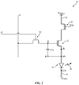
- a schematic diagram of an illustrative circuit for a pixel in an organic light-emitting diode display is shown in FIG. 2 .
- pixel 22 may include an organic light-emitting diode such as organic light-emitting diode 38 .
- a positive power supply voltage V DDEL may be supplied to positive power supply terminal 34 and a ground power supply voltage V SSEL may be supplied to ground power supply terminal 36 .
- Light-emitting diode 38 may emit colored light.
- organic light-emitting diode 38 may emit red light.
- Blue subpixels may have blue diodes 38 that emit blue light and green subpixels may have green diodes 38 that emit green light.
- Arrangements for display 14 in which pixels 22 have different colors may also be used.
- each pixel 22 the state of drive transistor 32 controls the amount of drive current I D flowing through diode 38 and therefore the amount of light 40 that is emitted from that pixel.
- Each diode 38 has an anode AN and a cathode CD.
- Drive current I D flows between anode AN and cathode CD.
- Cathode CD of diode 38 is coupled to ground terminal 36 , so cathode terminal CD of diode 38 may sometimes be referred to as the ground terminal for diode 38 .
- Cathode CD may be shared among multiple diodes (i.e., the cathodes CD of multiple diodes may be tied to a shared voltage).
- Each anode AN may be individually driven by a respective drive transistor 32 .
- pixel 22 may include a storage capacitor such as storage capacitor Cst.
- the voltage on storage capacitor Cst is applied to the gate of transistor 32 to control transistor 32 (i.e., to control the magnitude of drive current I D ).
- Data can be loaded into storage capacitor Cst using one or more switching transistors.
- One or more emission enable transistors may be used in controlling the flow of current through drive transistor 32 .
- transistor 30 serves as a switching transistor that controls data loading onto node A
- transistor 32 is a drive transistor
- transistor 42 is an emission enable transistor. Configurations for pixels such as pixel 22 with different numbers of transistors may be used, if desired.
- control signal G is being applied to the gate of switching transistor 30 (e.g., to turn on transistor 30 when it is desired to load data from data line D to node A) and control signal EM is being applied to the gate of emission enable transistor 42 (e.g., to disable transistor 32 during threshold voltage compensation and data loading operations and to enable transistor 32 during light emission operations).
- the control signals that are applied to pixel 22 may be applied to all of the pixels 22 in a row of display 14 at the same time and may be used for controlling the transistors in that row during threshold voltage compensation operations, data loading operations, and emission operations.
- FIG. 3 is a schematic diagram of an illustrative display in device 10 .
- display 14 may have an array of pixels 22 for displaying images for a user.
- the pixels of the array may be arranged in rows and columns. There may be any suitable number of rows and columns in the array of pixels 22 (e.g., ten or more, one hundred or more, or one thousand or more).
- the array of pixels 22 may include pixels 22 of different colors. As an example, display 14 may have red pixels that emit red light, green pixels that emit green light, and blue pixels that emit blue light. Configurations for display 14 that include pixels of other colors may be also be used, if desired.
- Display driver circuitry may be used to control the operation of pixels 22 .
- the display driver circuitry may be formed from integrated circuits, thin-film transistor circuits, or other suitable circuitry.
- Display driver circuitry 28 of FIG. 3 may contain communications circuitry for communicating with system control circuitry such as control circuitry 16 (e.g., a system-on-chip integrated circuit and/or other processing circuitry) over path 26 .
- Path 26 may be formed from traces on a flexible printed circuit or other cable and may be used for conveying image data and control signals between control circuitry 16 and display 14 .
- Path 26 may, as an example, carry a control signal such as variable refresh rate status signal VRR_STATUS that is used in selecting a desired refresh rate for display 14 .
- display 14 may display images corresponding to the image data received on path 26 .
- display driver circuitry 28 may supply image data to data lines D using digital-to-analog converter circuitry such as gamma block circuitry 52 while issuing clock signals and other control signals to supporting display driver circuitry such as gate driver circuitry 18 over path 50 .
- circuitry 28 may also supply clock signals and other control signals to gate driver circuitry on an opposing edge of display 14 .
- the circuits of display driver circuitry 28 and gate driver circuitry 18 allow data to be refreshed in the array of pixels 22 at various different refresh rates (i.e., display 14 is a variable refresh rate display).
- Gate driver circuitry 18 may be implemented as part of an integrated circuit and/or may be implemented using thin-film transistor circuitry.
- Horizontal control lines G in display 14 may supply gate line signals (scan line signals), emission enable control signals, and other horizontal control signals for controlling the pixels of each row.
- There may be any suitable number of horizontal control signals per row of pixels 22 e.g., one or more, two or more, three or more, four or more, etc.).
- Each column of pixels 22 receives image data on a corresponding data line D.
- data is loaded from data lines D into the pixels 22 of a given row of display 14 .
- Gate driver circuitry 18 contains circuitry such as shift register circuitry that asserts an output signal (or multiple output signals) in each row in succession, starting at the first row of pixels 22 and ending with the last row of pixels 22 . In this way, frames of image data may be loaded into display 14 for viewing by a user.
- Control circuitry 16 may analyze images that are to be displayed on display 14 by examining the contents of frame buffer 54 . Control circuitry 16 may, for example, examine the contents of frame buffer 54 to determine whether upcoming content that is to be displayed on display 14 contains moving content or static content.
- control circuitry 16 can analyze the image data in storage such as buffer 54 to determine whether image content is moving or static and may issue corresponding control signals on path 26 .
- control signals such as control signal VRR_STATUS may be deasserted when moving content is present and may be asserted when static content is present.
- Display driver circuitry 28 may adjust display control signals such as one or more clock and control signals on path 50 in response to the refresh rate control signal VRR_STATUS to ensure that display 14 is being refreshed at an appropriate rate.
- display driver circuitry 28 may use gamma block 52 to scale the magnitude of output data D in accordance with a scaling factor. The scaling factor can be adjusted as a function of time to minimize visible changes in the output of display 14 when transitioning between different refresh rates.
- the refresh rate of the display is dropped to 1 Hz, all 200 lines of the display will effectively be continuously on (i.e., the display luminance will rise to L from 0.995 L), which can cause the display to flicker.
- the same type of flickering can arise when transitioning from the low refresh rate (1 Hz) back to the high refresh rate (e.g., 60 Hz) associated with normal operation.
- FIG. 4 When a time-varying scaling factor is used to adjust the magnitude of data signals D, potentially abrupt display luminance variations such as these can be avoided.
- FIG. 4 The way in which this type of arrangement may be used in controlling the operation of display 14 is shown in FIG. 4 .
- display refresh rate for display 14 has been plotted as a function of time.
- moving images are being displayed at times before time t s and at times after time t f .
- time t s and t f In the period of time between t s and t f , only static content is being displayed.
- variable refresh rate of display 14 is initially set to a relatively high value of RRH.
- the high refresh rate is not needed to smoothly display images on display 14 , so the refresh rate can be lowered to a relatively low value of RRL.
- the magnitudes of RRH and RRL may have any suitable values. With one example, RRH is 60 Hz and RRL is 1 Hz. Other refresh rate values may be used when operating display 14 , if desired.
- the value of data D that is supplied to the array of pixels 22 in display 14 may be scaled using scaling factor SF. If, for example, a given data signal D has a voltage value of D 1 before scaling, the scaled value of D that is loaded into a given pixel would be SF*D 1 (i.e., D would be SF*D 1 after the scaling factor has been applied).
- scaling factor SF may be set to a first value SFH.
- scaling factor SF may be set to a second value SFL. Scaling factors adjustments may be made so as to reduce visible display artifacts such as flickering by balancing the luminance between the high refresh rate periods and low refresh rates periods.
- a default scaling factor SF of 1.0 may be applied to display 14 during operation at high refresh rate RRH.
- a scaling factor of 1.0 When a scaling factor of 1.0 is applied to data D, the luminance of display 14 will be 0.995 L during normal operation at rate RRH (in an illustrative example where display 14 has 200 rows of pixels 22 ).
- the scaling factor SF may be adjusted to 0.995.
- the time occupied by data loading relative to the frame period e.g., a 1 s frame period
- the luminance of display 14 would increase to 1.005 L when transitioning from rate RRH to rate RRL.
- the scaling factor SF may likewise be changed from 0.995 to 1.0 when returning to RRH from RRL at time t f . Further minimization of visible display artifacts can be accomplished by using additional scaling factor values during refresh rate transmissions (e.g., by using multiple different scaling factor values when moving from RRL to RRH at time t f ).
- FIGS. 5, 6, 7, 8, and 9 An illustrative scenario in which scaling factor SF is varied as display 14 transitions into and out of a low refresh rate mode of operation is set forth in the diagrams of FIGS. 5, 6, 7, 8, and 9 .
- display 14 has 200 rows of pixels 22 and has a luminance (light output) of L when all 200 rows of pixels 22 are simultaneously supplying output.
- display 14 is operated normally at high refresh rate RRH.
- one of the rows of pixels 22 is off at any given moment in time (in this example) so that data may be loaded into that row.
- This type of situation is illustrated in FIG. 5 in which rows of pixels 22 that are outputting light are labeled at being “ON,” while the row into which data is being loaded and that is not outputting any light is labeled as being “OFF.”
- the scaling factor SF in this situation is set to 1.0 and the resulting light output (luminance) of display 14 is 0.995 L.
- control circuitry 16 can detect that only static content will need to be displayed after time t s and can therefore assert variable refresh rate signal VRR_STATUS at time t s . This directs display driver circuitry 28 to use gamma block 52 to adjust the magnitude of the output data signals D by applying a scaling factor SF of 0.995.
- display 14 will be in a transitional state with mixed scaling factors. As shown in FIG. 6 , for example, rows above the OFF row will have been loaded with scaled data using the reduced scaling factor value of 0.995, whereas rows below the OFF row (i.e., the rows into which data has not yet been loaded) will still be using the original default scaling factor value of 1.0.
- display 14 will be operated at the low refresh rate of 1 Hz and all rows of pixels 22 in display 14 will effectively be continuously in the ON state, as shown in FIG. 7 . Because the scaling factor of 0.995 has been applied to the data in all of the rows of display 14 , the total luminance of display 14 will be 0.995 L. This is the same as the luminance value for display 14 at times before t s , so flickering in the output of display 14 is minimized.
- FIGS. 7 and 8 show how scaling factor SF may be adjusted when transitioning from the low refresh rate RRL to the high refresh rate at time t f .
- the rows of display 14 which were all on during the low refresh rate period will again have one row that is being used for data loading and is therefore off.
- the presence of the row of pixels that is off will decrease display luminance by 0.5% (in this example in which display 14 has 200 rows).
- display 14 may therefore initially use an increased scaling factor of 1.005 in anticipation of the drop in luminance that will be produced due to the presence of the OFF row.
- This enhanced scaling factor value helps to compensate for the decrease in luminance that results from the OFF row and therefore helps to even out luminance variations.
- the scaling factor may be reduced to a lower value such as 1.0, as illustrated on the right side of FIG. 8 .
- the value of 1.0 may then be sustained during the use of high refresh rate RRH at times greater than t f , as shown in FIG. 9 .
- FIG. 8 Using the transitional scheme of FIG. 8 in which the scaling factor is momentarily increased before being returned to its default value, visible display artifacts may be minimized when transitioning from rate RRL to rate RRH.
- Other scaling factors and other changes in the scaling factor as a function of time and refresh rate may be used if desired.
- the illustrative arrangement of FIGS. 5, 6, 7, 8, and 9 is merely illustrative.
- FIG. 10 is a flow chart of illustrative steps involved in operating device 10 in a configuration in which device 10 has a display with a variable refresh rate and an adjustable scaling factor.
- step 90 device 10 presents moving content on display 14 at a high refresh rate RRH (e.g., 60 Hz).
- Control circuitry 16 may sense the presence of moving content by analyzing frame buffer 54 . So long as moving content is being displayed, variable refresh rate control signal VRR_STATUS may be deasserted so that display driver circuitry 28 (and digital-to-analog converter circuitry such as gamma block 52 ) will apply a default scaling factor of 1.0 to the data signals D being supplied to the rows of pixels 22 in display 14 .
- control circuitry 16 may continue to analyze the image data that is to be displayed on display 14 (e.g., frame buffer information can be analyzed to determine whether static content is present).
- control circuitry 16 may assert the VRR_STATUS control signal or may otherwise direct display driver circuitry 28 and gamma block 52 apply a reduced scaling factor of 0.995 to the data being loaded into display 14 (step 92 ).
- the refresh rate of display 14 may be adjusted from RRH to RRL to conserve power.
- control circuitry 16 may analyze the content in frame buffer 54 , may monitor input-output devices 12 for a user input or a sensor input, or may otherwise monitor device 10 for the satisfaction of criteria indicative of an upcoming need to display moving content on display 14 .
- control circuitry 16 may deassert control signal VRR_STATUS and the refresh rate for display 14 may be increased to high refresh rate RRH to ensure that the moving content is displayed satisfactorily (step 96 ).
- display driver circuitry 28 may, in response to detection of the deassertion of VRR_STATUS, raise the scaling factor SF to an elevated value (e.g., 1.005) and then lower the scaling factor SF to the default value of 1.0. As described in connection with FIG. 8 , this adjustment of the scaling factor may help minimize luminance variations for display 14 during the transition between rate RRL and rate RRH.
- processing may loop back to step 90 for additional operation of display 14 at high refresh rate RRH, as indicated by line 98 .
Landscapes
- Engineering & Computer Science (AREA)
- Physics & Mathematics (AREA)
- Computer Hardware Design (AREA)
- General Physics & Mathematics (AREA)
- Theoretical Computer Science (AREA)
- Control Of Indicators Other Than Cathode Ray Tubes (AREA)
- Multimedia (AREA)
Abstract
Description
Claims (19)
Priority Applications (1)
| Application Number | Priority Date | Filing Date | Title |
|---|---|---|---|
| US14/591,354 US11468809B2 (en) | 2015-01-07 | 2015-01-07 | Low-flicker variable refresh rate display |
Applications Claiming Priority (1)
| Application Number | Priority Date | Filing Date | Title |
|---|---|---|---|
| US14/591,354 US11468809B2 (en) | 2015-01-07 | 2015-01-07 | Low-flicker variable refresh rate display |
Publications (2)
| Publication Number | Publication Date |
|---|---|
| US20160196802A1 US20160196802A1 (en) | 2016-07-07 |
| US11468809B2 true US11468809B2 (en) | 2022-10-11 |
Family
ID=56286830
Family Applications (1)
| Application Number | Title | Priority Date | Filing Date |
|---|---|---|---|
| US14/591,354 Active 2039-01-07 US11468809B2 (en) | 2015-01-07 | 2015-01-07 | Low-flicker variable refresh rate display |
Country Status (1)
| Country | Link |
|---|---|
| US (1) | US11468809B2 (en) |
Families Citing this family (20)
| Publication number | Priority date | Publication date | Assignee | Title |
|---|---|---|---|---|
| US10467964B2 (en) * | 2015-09-29 | 2019-11-05 | Apple Inc. | Device and method for emission driving of a variable refresh rate display |
| US10147370B2 (en) * | 2015-10-29 | 2018-12-04 | Nvidia Corporation | Variable refresh rate gamma correction |
| KR102370340B1 (en) | 2017-05-24 | 2022-03-07 | 삼성디스플레이 주식회사 | Organic light emitting display device and method of operating the same |
| KR102527296B1 (en) * | 2018-05-04 | 2023-05-02 | 삼성디스플레이 주식회사 | Display system and method of synchronizing a frame driving timing for the same |
| US11159798B2 (en) * | 2018-08-21 | 2021-10-26 | International Business Machines Corporation | Video compression using cognitive semantics object analysis |
| US11094296B2 (en) * | 2018-12-05 | 2021-08-17 | Google Llc | Varying display refresh rate |
| US10852815B2 (en) * | 2019-04-30 | 2020-12-01 | Valve Corporation | Display system with dynamic light output adjustment for maintaining constant brightness |
| KR102697934B1 (en) * | 2019-07-29 | 2024-08-26 | 삼성디스플레이 주식회사 | Display device and method of driving the same |
| KR102707922B1 (en) | 2020-02-10 | 2024-09-23 | 삼성전자주식회사 | Electronic device including a display and method of operating the same |
| US11830457B2 (en) | 2020-08-28 | 2023-11-28 | Google Llc | Adjusting peak signal in transitional frame |
| KR102865967B1 (en) * | 2021-05-10 | 2025-09-29 | 구글 엘엘씨 | Disable switching when encoded intensity is low |
| CN113593466B (en) * | 2021-05-18 | 2024-02-09 | 昆山国显光电有限公司 | Display panel driving method, display device and storage medium |
| KR20230034464A (en) | 2021-09-02 | 2023-03-10 | 삼성디스플레이 주식회사 | Display device and method of operating the display device |
| CN114023238B (en) * | 2021-11-16 | 2023-05-05 | Tcl华星光电技术有限公司 | Display device |
| KR20240015988A (en) * | 2022-07-28 | 2024-02-06 | 엘지디스플레이 주식회사 | Display device |
| KR20240104836A (en) * | 2022-12-28 | 2024-07-05 | 엘지디스플레이 주식회사 | Light emitting display apparatus |
| CN116825042B (en) * | 2023-04-19 | 2024-05-17 | 惠科股份有限公司 | Gamma voltage adjusting method, gamma voltage adjusting circuit and display device |
| WO2025137911A1 (en) * | 2023-12-27 | 2025-07-03 | 京东方科技集团股份有限公司 | Pixel circuit, driving method, and display apparatus |
| CN121053903A (en) * | 2024-05-29 | 2025-12-02 | 武汉华星光电半导体显示技术有限公司 | Display panel and display device |
| CN119693333B (en) * | 2024-12-04 | 2025-10-14 | 东莞市长建电子有限公司 | A production detection method for dynamic refresh rate of display screen |
Citations (17)
| Publication number | Priority date | Publication date | Assignee | Title |
|---|---|---|---|---|
| US20010028346A1 (en) * | 1997-04-15 | 2001-10-11 | Yasuyuki Kudo | Liquid crystal display control apparatus and liquid crystal display apparatus |
| US20020036603A1 (en) * | 2000-06-05 | 2002-03-28 | Pioneer Corporation | Display device |
| US20020154077A1 (en) | 2000-02-10 | 2002-10-24 | Naohide Wakita | Display element and driving method |
| US20030184569A1 (en) * | 2002-03-28 | 2003-10-02 | Nec Corporation | Image display method and image display device |
| US20050280615A1 (en) * | 2004-06-16 | 2005-12-22 | Eastman Kodak Company | Method and apparatus for uniformity and brightness correction in an oled display |
| US20060146005A1 (en) * | 2005-01-06 | 2006-07-06 | Masahiro Baba | Image display device and method of displaying image |
| US20100149167A1 (en) * | 2008-12-17 | 2010-06-17 | Sony Corporation | Emissive type display device, semiconductor device, electronic device, and power supply line driving method |
| US20110187754A1 (en) * | 2010-02-03 | 2011-08-04 | Samsung Mobile Display Co., Ltd. | Organic light emitting display device and driving method threreof |
| US20120081419A1 (en) * | 2010-10-01 | 2012-04-05 | Canon Kabushiki Kaisha | Image display apparatus and control method thereof |
| US8228354B2 (en) | 2006-12-28 | 2012-07-24 | Rohm Co., Ltd. | Display control device with frame rate control |
| US20120256818A1 (en) | 2004-07-21 | 2012-10-11 | Sony Corporation | Display apparatus and method, storage medium, and program |
| US20140063078A1 (en) * | 2012-08-30 | 2014-03-06 | Samsung Display Co., Ltd. | Method of controlling a dimming operation, dimming operation control device, and flat panel display device having the same |
| US9197847B2 (en) * | 2009-06-16 | 2015-11-24 | Joled Inc. | Image display device, image display method, and program |
| US9230476B2 (en) * | 2012-10-16 | 2016-01-05 | Samsung Electronics Co., Ltd. | Method and electronic device for reducing power consumption of display |
| US9251756B2 (en) * | 2013-04-11 | 2016-02-02 | Samsung Display Co., Ltd. | Display device |
| US9613554B2 (en) * | 2012-09-24 | 2017-04-04 | Samsung Display Co., Ltd. | Display driving method and integrated driving apparatus thereof |
| US9728142B2 (en) * | 2015-07-15 | 2017-08-08 | Christie Digital Systems Usa, Inc. | Reduced blur, low flicker display system |
-
2015
- 2015-01-07 US US14/591,354 patent/US11468809B2/en active Active
Patent Citations (18)
| Publication number | Priority date | Publication date | Assignee | Title |
|---|---|---|---|---|
| US20010028346A1 (en) * | 1997-04-15 | 2001-10-11 | Yasuyuki Kudo | Liquid crystal display control apparatus and liquid crystal display apparatus |
| US20020154077A1 (en) | 2000-02-10 | 2002-10-24 | Naohide Wakita | Display element and driving method |
| US20020036603A1 (en) * | 2000-06-05 | 2002-03-28 | Pioneer Corporation | Display device |
| US20030184569A1 (en) * | 2002-03-28 | 2003-10-02 | Nec Corporation | Image display method and image display device |
| US20050280615A1 (en) * | 2004-06-16 | 2005-12-22 | Eastman Kodak Company | Method and apparatus for uniformity and brightness correction in an oled display |
| US20120256818A1 (en) | 2004-07-21 | 2012-10-11 | Sony Corporation | Display apparatus and method, storage medium, and program |
| US20060146005A1 (en) * | 2005-01-06 | 2006-07-06 | Masahiro Baba | Image display device and method of displaying image |
| US8228354B2 (en) | 2006-12-28 | 2012-07-24 | Rohm Co., Ltd. | Display control device with frame rate control |
| US20100149167A1 (en) * | 2008-12-17 | 2010-06-17 | Sony Corporation | Emissive type display device, semiconductor device, electronic device, and power supply line driving method |
| US8570314B2 (en) | 2008-12-17 | 2013-10-29 | Sony Corporation | Emissive type display device, semiconductor device, electronic device, and power supply line driving method |
| US9197847B2 (en) * | 2009-06-16 | 2015-11-24 | Joled Inc. | Image display device, image display method, and program |
| US20110187754A1 (en) * | 2010-02-03 | 2011-08-04 | Samsung Mobile Display Co., Ltd. | Organic light emitting display device and driving method threreof |
| US20120081419A1 (en) * | 2010-10-01 | 2012-04-05 | Canon Kabushiki Kaisha | Image display apparatus and control method thereof |
| US20140063078A1 (en) * | 2012-08-30 | 2014-03-06 | Samsung Display Co., Ltd. | Method of controlling a dimming operation, dimming operation control device, and flat panel display device having the same |
| US9613554B2 (en) * | 2012-09-24 | 2017-04-04 | Samsung Display Co., Ltd. | Display driving method and integrated driving apparatus thereof |
| US9230476B2 (en) * | 2012-10-16 | 2016-01-05 | Samsung Electronics Co., Ltd. | Method and electronic device for reducing power consumption of display |
| US9251756B2 (en) * | 2013-04-11 | 2016-02-02 | Samsung Display Co., Ltd. | Display device |
| US9728142B2 (en) * | 2015-07-15 | 2017-08-08 | Christie Digital Systems Usa, Inc. | Reduced blur, low flicker display system |
Also Published As
| Publication number | Publication date |
|---|---|
| US20160196802A1 (en) | 2016-07-07 |
Similar Documents
| Publication | Publication Date | Title |
|---|---|---|
| US11468809B2 (en) | Low-flicker variable refresh rate display | |
| CN113450711B (en) | Display device, driving method thereof and driving device | |
| KR20240015130A (en) | Display device and driving method thereof | |
| US11373602B2 (en) | Pixel circuit, method and apparatus for driving the same, array substrate, and display apparatus | |
| US20200118497A1 (en) | Displays with Multiple Scanning Modes | |
| US9740046B2 (en) | Method and apparatus to provide a lower power user interface on an LCD panel through localized backlight control | |
| US9524694B2 (en) | Display with spatial and temporal refresh rate buffers | |
| KR102876113B1 (en) | Display device having a variable driving frequency | |
| EP2889860B1 (en) | Organic light emitting diode display device and method of driving the same | |
| CN103854600B (en) | Organic LED display device and driving method thereof | |
| US8207958B2 (en) | Display having rush current reduction during power-on | |
| US20160275897A1 (en) | Content-driven slew rate control for display driver | |
| JP2011107677A (en) | Display device and method for driving the same | |
| CN113257164B (en) | Display device and driving method thereof | |
| KR20130123218A (en) | Organic light-emitting diode display, circuit and method for driving thereof | |
| US20190325816A1 (en) | Pre-compensation for pre-toggling-induced artifacts in electronic displays | |
| US8933866B2 (en) | Active matrix pixel brightness control | |
| US20210287613A1 (en) | Voltage control circuit and power supply voltage control method, and display device | |
| US12334010B2 (en) | Display device | |
| CN101211530A (en) | Peak intensity level control device and method, self-luminous display device | |
| KR20180033001A (en) | Organic light emitting display panel, organic light emitting display device, data driver, and low power driving method | |
| KR20140030468A (en) | Method of controlling a dimming operation, dimming operation control device, and flat panel display device having the same | |
| US10217420B2 (en) | Display apparatus and method of controlling luminance thereof | |
| CN111583871A (en) | Pixel driving circuit, display panel and electronic device | |
| CN110534054B (en) | Display driving method and device, display device, storage medium, chip |
Legal Events
| Date | Code | Title | Description |
|---|---|---|---|
| AS | Assignment |
Owner name: APPLE INC., CALIFORNIA Free format text: ASSIGNMENT OF ASSIGNORS INTEREST;ASSIGNORS:NHO, HYUNWOO;CHEN, WEI;YAO, WEI;AND OTHERS;SIGNING DATES FROM 20141208 TO 20150105;REEL/FRAME:034656/0088 |
|
| AS | Assignment |
Owner name: APPLE INC., CALIFORNIA Free format text: CORRECTIVE ASSIGNMENT TO CORRECT THE FOURTH INVENTOR'S NAME PREVIOUSLY RECORDED AT REEL: 034656 FRAME: 0088. ASSIGNOR(S) HEREBY CONFIRMS THE ASSIGNMENT;ASSIGNORS:NHO, HYUNWOO;CHEN, WEI;YAO, WEI H.;AND OTHERS;SIGNING DATES FROM 20141208 TO 20150105;REEL/FRAME:035071/0159 |
|
| STPP | Information on status: patent application and granting procedure in general |
Free format text: DOCKETED NEW CASE - READY FOR EXAMINATION |
|
| STPP | Information on status: patent application and granting procedure in general |
Free format text: NON FINAL ACTION MAILED |
|
| STPP | Information on status: patent application and granting procedure in general |
Free format text: RESPONSE TO NON-FINAL OFFICE ACTION ENTERED AND FORWARDED TO EXAMINER |
|
| STPP | Information on status: patent application and granting procedure in general |
Free format text: FINAL REJECTION MAILED |
|
| STCV | Information on status: appeal procedure |
Free format text: NOTICE OF APPEAL FILED |
|
| STCV | Information on status: appeal procedure |
Free format text: ON APPEAL -- AWAITING DECISION BY THE BOARD OF APPEALS |
|
| STCV | Information on status: appeal procedure |
Free format text: BOARD OF APPEALS DECISION RENDERED |
|
| STPP | Information on status: patent application and granting procedure in general |
Free format text: NOTICE OF ALLOWANCE MAILED -- APPLICATION RECEIVED IN OFFICE OF PUBLICATIONS |
|
| STPP | Information on status: patent application and granting procedure in general |
Free format text: PUBLICATIONS -- ISSUE FEE PAYMENT VERIFIED |
|
| STCF | Information on status: patent grant |
Free format text: PATENTED CASE |