WO2010146914A1 - 照明装置、表示装置、及びテレビ受信装置 - Google Patents
照明装置、表示装置、及びテレビ受信装置 Download PDFInfo
- Publication number
- WO2010146914A1 WO2010146914A1 PCT/JP2010/056205 JP2010056205W WO2010146914A1 WO 2010146914 A1 WO2010146914 A1 WO 2010146914A1 JP 2010056205 W JP2010056205 W JP 2010056205W WO 2010146914 A1 WO2010146914 A1 WO 2010146914A1
- Authority
- WO
- WIPO (PCT)
- Prior art keywords
- light source
- substrate
- chassis
- led
- main body
- Prior art date
Links
Images


Classifications
-
- G—PHYSICS
- G02—OPTICS
- G02F—OPTICAL DEVICES OR ARRANGEMENTS FOR THE CONTROL OF LIGHT BY MODIFICATION OF THE OPTICAL PROPERTIES OF THE MEDIA OF THE ELEMENTS INVOLVED THEREIN; NON-LINEAR OPTICS; FREQUENCY-CHANGING OF LIGHT; OPTICAL LOGIC ELEMENTS; OPTICAL ANALOGUE/DIGITAL CONVERTERS
- G02F1/00—Devices or arrangements for the control of the intensity, colour, phase, polarisation or direction of light arriving from an independent light source, e.g. switching, gating or modulating; Non-linear optics
- G02F1/01—Devices or arrangements for the control of the intensity, colour, phase, polarisation or direction of light arriving from an independent light source, e.g. switching, gating or modulating; Non-linear optics for the control of the intensity, phase, polarisation or colour
- G02F1/13—Devices or arrangements for the control of the intensity, colour, phase, polarisation or direction of light arriving from an independent light source, e.g. switching, gating or modulating; Non-linear optics for the control of the intensity, phase, polarisation or colour based on liquid crystals, e.g. single liquid crystal display cells
- G02F1/133—Constructional arrangements; Operation of liquid crystal cells; Circuit arrangements
- G02F1/1333—Constructional arrangements; Manufacturing methods
- G02F1/1335—Structural association of cells with optical devices, e.g. polarisers or reflectors
- G02F1/1336—Illuminating devices
- G02F1/133602—Direct backlight
- G02F1/133603—Direct backlight with LEDs
-
- G—PHYSICS
- G02—OPTICS
- G02F—OPTICAL DEVICES OR ARRANGEMENTS FOR THE CONTROL OF LIGHT BY MODIFICATION OF THE OPTICAL PROPERTIES OF THE MEDIA OF THE ELEMENTS INVOLVED THEREIN; NON-LINEAR OPTICS; FREQUENCY-CHANGING OF LIGHT; OPTICAL LOGIC ELEMENTS; OPTICAL ANALOGUE/DIGITAL CONVERTERS
- G02F1/00—Devices or arrangements for the control of the intensity, colour, phase, polarisation or direction of light arriving from an independent light source, e.g. switching, gating or modulating; Non-linear optics
- G02F1/01—Devices or arrangements for the control of the intensity, colour, phase, polarisation or direction of light arriving from an independent light source, e.g. switching, gating or modulating; Non-linear optics for the control of the intensity, phase, polarisation or colour
- G02F1/13—Devices or arrangements for the control of the intensity, colour, phase, polarisation or direction of light arriving from an independent light source, e.g. switching, gating or modulating; Non-linear optics for the control of the intensity, phase, polarisation or colour based on liquid crystals, e.g. single liquid crystal display cells
- G02F1/133—Constructional arrangements; Operation of liquid crystal cells; Circuit arrangements
- G02F1/1333—Constructional arrangements; Manufacturing methods
- G02F1/1335—Structural association of cells with optical devices, e.g. polarisers or reflectors
- G02F1/1336—Illuminating devices
- G02F1/133602—Direct backlight
- G02F1/133608—Direct backlight including particular frames or supporting means
-
- G—PHYSICS
- G02—OPTICS
- G02F—OPTICAL DEVICES OR ARRANGEMENTS FOR THE CONTROL OF LIGHT BY MODIFICATION OF THE OPTICAL PROPERTIES OF THE MEDIA OF THE ELEMENTS INVOLVED THEREIN; NON-LINEAR OPTICS; FREQUENCY-CHANGING OF LIGHT; OPTICAL LOGIC ELEMENTS; OPTICAL ANALOGUE/DIGITAL CONVERTERS
- G02F1/00—Devices or arrangements for the control of the intensity, colour, phase, polarisation or direction of light arriving from an independent light source, e.g. switching, gating or modulating; Non-linear optics
- G02F1/01—Devices or arrangements for the control of the intensity, colour, phase, polarisation or direction of light arriving from an independent light source, e.g. switching, gating or modulating; Non-linear optics for the control of the intensity, phase, polarisation or colour
- G02F1/13—Devices or arrangements for the control of the intensity, colour, phase, polarisation or direction of light arriving from an independent light source, e.g. switching, gating or modulating; Non-linear optics for the control of the intensity, phase, polarisation or colour based on liquid crystals, e.g. single liquid crystal display cells
- G02F1/133—Constructional arrangements; Operation of liquid crystal cells; Circuit arrangements
- G02F1/1333—Constructional arrangements; Manufacturing methods
- G02F1/133308—Support structures for LCD panels, e.g. frames or bezels
- G02F1/133314—Back frames
-
- G—PHYSICS
- G02—OPTICS
- G02F—OPTICAL DEVICES OR ARRANGEMENTS FOR THE CONTROL OF LIGHT BY MODIFICATION OF THE OPTICAL PROPERTIES OF THE MEDIA OF THE ELEMENTS INVOLVED THEREIN; NON-LINEAR OPTICS; FREQUENCY-CHANGING OF LIGHT; OPTICAL LOGIC ELEMENTS; OPTICAL ANALOGUE/DIGITAL CONVERTERS
- G02F2201/00—Constructional arrangements not provided for in groups G02F1/00 - G02F7/00
- G02F2201/46—Fixing elements
- G02F2201/465—Snap -fit
Definitions
- the present invention relates to a lighting device, a display device, and a television receiver.
- a liquid crystal panel used in a liquid crystal display device such as a liquid crystal television does not emit light, and thus requires a separate backlight device as an illumination device.
- the backlight device is installed on the back side of the liquid crystal panel (the side opposite to the display surface).
- the chassis has an open surface on the liquid crystal panel side, a light source accommodated in the chassis, And an optical member (such as a diffusion sheet) that is disposed in the opening and efficiently emits light emitted from the light source toward the liquid crystal panel.
- an LED may be used as a light source.
- an LED substrate on which the LED is mounted is accommodated in the chassis.
- the present invention has been completed based on the above circumstances, and an object thereof is to stably fix a light source substrate without using screws.
- An illuminating device of the present invention includes a light source substrate having a light source, a chassis having an opening for receiving the light source substrate and emitting light from the light source, and extending in at least one direction along a plate surface of the light source substrate. And a holding member fixed to the chassis with the light source substrate sandwiched between the chassis and the chassis.
- the light source substrate is held in a state of being sandwiched between the holding member and the chassis. Since the light source substrate is fixed by using a holding member extending in at least one direction along the plate surface of the light source substrate, a screw having a dot shape with respect to the plate surface of the light source substrate is used. Compared to the case where the light source substrate is used, the light source substrate can be stably fixed even if the number of holding members to be used is small. Since the number of holding members used can be reduced, the number of parts and the number of assembling steps can be reduced, and the work efficiency can be improved. Since the light source board can be stably fixed, the optical characteristics when the light emitted from the light source is emitted from the opening of the chassis can be stabilized, and the heat radiation from the light source board to the chassis can be stabilized. Can be stabilized.
- the holding member includes a main body that sandwiches the light source substrate with the chassis, and a fixing portion that protrudes from the main body toward the chassis and is fixed to the chassis. In this way, the light source substrate sandwiched between the main body portion and the chassis can be suitably fixed by fixing the fixing portion to the chassis.
- the fixing portion is disposed at a position where the fixing portion does not overlap with the light source substrate in a plan view in the main body portion. In this way, the fixing part can be fixed to the chassis without penetrating the light source substrate. Thereby, since a hole or the like for passing the fixing portion through the light source substrate is not formed, the manufacturing cost of the light source substrate can be reduced and the circuit design can be facilitated.
- the main body is configured to straddle the light source substrate, and a pair of the fixing portions is provided at a position sandwiching the light source substrate in the main body as viewed in a plane. If it does in this way, a light source substrate can be stably fixed by the main-body part of the form straddling a light source substrate. In addition, by fixing the pair of fixing portions to the chassis, the light source substrate disposed between the two fixing portions can be more stably fixed in a plan view.
- a substrate contact portion that protrudes toward the light source substrate and directly or indirectly contacts the light source substrate at a position overlapping with the light source substrate in a plan view in the main body. Is provided. In this way, since the light source substrate can be pressed by the substrate contact portion, it is difficult for the light source substrate to rattle due to dimensional tolerances, and the light source substrate can be stably fixed. be able to. Furthermore, depending on the setting of the projecting dimension of the substrate contact portion, when the fixed portion is fixed to the chassis while the substrate contact portion is in direct or indirect contact with the light source substrate, the fixed portion is used as a fulcrum. It may be possible to elastically warp and deform the main body portion to the side opposite to the light source substrate side. Therefore, in this way, the light source substrate can be brought into close contact with the chassis by the elastic force of the warped and deformed main body, and the light source substrate can be more stably fixed.
- a reflection member that reflects light toward the opening is disposed in the chassis, and the reflection member is inserted into a light source through which the light source passes at a position overlapping the light source when seen in a plan view.
- the substrate contact portion is passed through the substrate contact portion insertion hole of the reflecting member, the light source substrate can be directly pressed by the substrate contact portion, and rattling of the light source substrate is more effectively prevented. be able to.
- the protruding dimension of the substrate contact portion from the main body is larger than the thickness of the reflecting member.
- the light source substrate has a rectangular shape in plan view, and the main body is configured to extend along the short side direction of the light source substrate. If it does in this way, compared with the case where the main-body part is made into the form extended along the long side direction in a light source board
- the main body is configured to straddle the light source substrate. In this way, the light source substrate can be more stably fixed.
- a plurality of the light source boards are arranged in the chassis so as to be parallel to each other, and the main body is configured to extend over the plurality of light source boards. In this way, a plurality of light source boards can be fixed by a single holding member, which is suitable for reducing the number of components.
- the main body is configured to straddle a plurality of the light source substrates. In this way, since the main body is sandwiched between the chassis with the plurality of light source boards straddling the plurality of light source boards, the plurality of light source boards can be more stably fixed.
- a plurality of the light sources are arranged in parallel along the long side direction of the light source substrate. If it does in this way, a plurality of light sources can be efficiently arranged to a light source substrate, and it becomes suitable for high brightness etc.
- the main body is arranged to pass between the adjacent light sources. In this way, the space held between adjacent light sources can be used effectively. Further, it is possible to prevent the main body from obstructing the light emitted from the light source.
- the holding member is disposed at two positions spaced apart in the long side direction of the light source substrate. In this way, the light source substrate can be stably fixed even if the holding member has a configuration in which the main body portion extends along the short side direction of the light source substrate and is downsized.
- the chassis has a rectangular shape when viewed from above, and a plurality of the light source substrates are arranged in parallel in a state where the long side direction thereof coincides with the long side direction of the chassis. In this way, it is possible to reduce the number of light source boards arranged in the chassis as compared with the case where a plurality of light source boards are arranged in parallel with the long side direction being coincident with the short side direction of the chassis. it can. Therefore, the number of lighting circuits and the like necessary for lighting the light sources arranged on each light source substrate can be reduced, which is suitable for cost reduction.
- the fixing portion penetrates the chassis and is locked to the chassis from the side opposite to the light source substrate side. In this way, since the holding member and the light source board can be fixed by locking the fixing portion penetrating the chassis to the chassis, it is not necessary to use other fixing means such as an adhesive, and low Fixing can be achieved easily at a low cost.
- An optical member arranged to cover the opening so as to face the light source substrate is provided, and the main body has a support that protrudes toward the optical member and can support the optical member. Is provided. If it does in this way, the function to support an optical member can be given to the holding member which fixes a light source board.
- the fixed portion and the support portion are arranged at positions that overlap each other when seen in a plane. In this way, when the operator attaches the holding member while gripping the support portion, the position of the fixed portion can be easily grasped, so that the workability is excellent.
- the fixed portion and the support portion are arranged at positions that are concentric with each other. In this way, workability is further improved.
- the chassis is provided with a substrate positioning portion capable of positioning the light source substrate in a direction along the plate surface.
- a substrate positioning portion capable of positioning the light source substrate in a direction along the plate surface.
- the substrate positioning portion is configured to extend along an edge portion of the light source substrate. In this way, the light source substrate can be easily and appropriately positioned by directing the edge of the light source substrate to the substrate positioning portion.
- the substrate positioning portion is formed to have a substrate accommodating space capable of accommodating the light source substrate from the opening side by partially protruding the chassis to the side opposite to the opening. Yes.
- the light source substrate can be accommodated from the opening side in the substrate accommodating space held by the substrate positioning unit, the light source substrate is opposite to the opening side by the depth of the substrate positioning unit. It will be placed in the position retracted to the side. Therefore, it is possible to secure a long optical path length until the light emitted from the light source reaches the opening by the amount of the retraction, so that the outgoing light emitted from the opening is less likely to be uneven.
- a reflection member that reflects light toward the opening is disposed in the chassis, and the reflection member has a light source insertion hole through which the light source passes at a position overlapping the light source when seen in a plan view. And is formed so as to cover a wider range than the substrate positioning portion in a plan view and is sandwiched between the main body portion and the light source substrate. If it does in this way, in addition to being able to fix a reflecting member with a light source board
- the light source substrate is disposed at a position retracted to the opposite side to the opening side by the depth of the substrate positioning portion, a step that may occur between the chassis and the light source substrate can be reduced. Accordingly, the reflection member having a wider range than the substrate positioning portion in a plan view is unlikely to be deformed such as warpage due to the step, and thus the light reflected by the reflection member is less likely to be uneven.
- the board positioning portion is formed so that a protruding dimension of the chassis toward the side opposite to the opening side is substantially equal to a plate thickness dimension of the light source board. In this way, the level difference that can occur between the chassis and the light source substrate can be almost eliminated, so that it is possible to prevent the reflection member from being deformed due to the level difference.
- the light source substrate has a rectangular shape when seen in a plan view, and the substrate positioning portion extends along a long side direction of the light source substrate. If it does in this way, the light source board which makes a rectangular shape can be positioned more easily and appropriately.
- the substrate positioning unit can position the light source substrate in two directions along the plate surface and orthogonal to each other. In this way, the light source substrate can be accurately positioned two-dimensionally.
- a reflection member that reflects light toward the opening is disposed in the chassis, and the reflection member is disposed closer to the opening than the light source substrate and is viewed in a plan view.
- a light source insertion hole through which the light source passes is provided at a position overlapping the light source. If it does in this way, light can be used effectively by reflecting light to the opening side by a reflective member, and it becomes suitable for improvement of a brightness, etc. Moreover, since the reflection member has the light source insertion hole, it is avoided that the emission of light from the light source is hindered.
- a diffusion lens for diffusing light from the light source is disposed on the opening side of the light source substrate at a position overlapping the light source when seen in a plan view. In this way, the light emitted from the light source can be diffused by the diffusion lens and then guided to the opening. Thereby, unevenness is less likely to occur in the outgoing light emitted from the opening.
- the reflection member is interposed between the first reflection member having a size that allows the light source insertion hole to pass the diffusion lens, and the light source substrate and the diffusion lens, and is viewed in a plane. And a second reflecting member that is disposed at a position overlapping the light source insertion hole provided in the first reflecting member and reflects light toward the diffuser lens. In this way, even if a light source insertion hole having a size for allowing the diffusion lens to pass through is provided in the first reflection member, the light is diffused by the second reflection member disposed at a position overlapping the light source insertion hole. Can be reflected to the side. As a result, light can be used effectively, which is suitable for improving luminance.
- the edge of the light source insertion hole in the first reflecting member and the second reflecting member are formed so as to overlap each other when seen in a plane. If it does in this way, the edge part of the light source penetration hole in the 1st reflective member and the 2nd reflective member will be connected seamlessly seeing in a plane. Thereby, light can be utilized more effectively.
- the reflection member is sandwiched between the holding member and the light source substrate. If it does in this way, a reflective member can also be fixed with a light source substrate by a holding member.
- the light source is an LED. In this way, high brightness and low power consumption can be achieved.
- a display device of the present invention includes the above-described illumination device and a display panel that performs display using light from the illumination device.
- the display device since the lighting device that supplies light to the display panel has a reduced number of parts and assembly steps, the display device can also be reduced in cost and improved in work efficiency. It becomes possible.
- a liquid crystal panel can be exemplified as the display panel.
- Such a display device can be applied as a liquid crystal display device to various uses such as a display of a television or a personal computer, and is particularly suitable for a large screen.
- the light source substrate can be stably fixed without using screws.
- FIG. 1 is an exploded perspective view showing a schematic configuration of a television receiver according to Embodiment 1 of the present invention.
- the exploded perspective view which shows schematic structure of the liquid crystal display device with which a television receiver is equipped
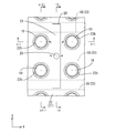
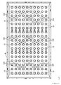
- the top view which shows the arrangement configuration of the LED board and holding member in the chassis with which a liquid crystal display device is equipped.
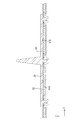
- FIG. 3 is a cross-sectional view taken along the line v-v in FIG.
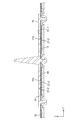
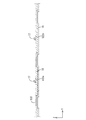
- the top view which shows the detailed arrangement structure of a LED board and a holding member Vii-vii sectional view of FIG. Viii-viii sectional view of FIG. Sectional view taken along line ix-ix in FIG.
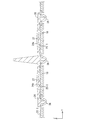
- Plan view of LED board The top view which shows the state (light source unit) which attached the 2nd reflective sheet and the diffusion lens to the LED board.
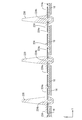
- Top view of holding member Bottom view of holding member Sectional view taken along line ix-ix in FIG. 6 showing a state before the holding member is attached to the chassis.
- Sectional drawing which shows the state before attaching the holding member which concerns on the modification 1 of Embodiment 1 to a chassis.
- Sectional drawing which shows the state which attached the holding member to the chassis
- Sectional drawing which shows the state which attached the holding member which concerns on the modification 2 of Embodiment 1 to the chassis.
- Sectional drawing which shows the state before attaching the holding member which concerns on the modification 3 of Embodiment 1 to a chassis.
- Sectional drawing which shows the state which attached the holding member to the chassis Sectional drawing which shows the relationship between the LED board which concerns on the modification 4 of Embodiment 1, a diffuser lens, a board
- Sectional drawing which shows the state which attached the holding member to the chassis Sectional drawing which shows the backlight apparatus which concerns on Embodiment 6 of this invention. Sectional drawing which shows the state which attached the holding member which concerns on other embodiment (1) of this invention to the chassis. Sectional drawing which shows the relationship between the chassis which concerns on other embodiment (2) of this invention, and an LED board. Sectional drawing which shows the relationship between the chassis which concerns on other embodiment (3) of this invention, and an LED board.
- FIGS. 1 A first embodiment of the present invention will be described with reference to FIGS.
- the liquid crystal display device 10 is illustrated.
- a part of each drawing shows an X axis, a Y axis, and a Z axis, and each axis direction is drawn to be a direction shown in each drawing.
- the upper side shown in FIG.4 and FIG.5 be a front side, and let the lower side of the figure be a back side.
- the television receiver TV includes a liquid crystal display device 10, front and back cabinets Ca and Cb that are accommodated so as to sandwich the liquid crystal display device 10, a power source P, a tuner T, And a stand S.
- the liquid crystal display device (display device) 10 has a horizontally long rectangular shape (rectangular shape) as a whole and is accommodated in a vertically placed state.
- the liquid crystal display device 10 includes a liquid crystal panel 11 that is a display panel and a backlight device (illumination device) 12 that is an external light source, which are integrated by a frame-like bezel 13 or the like. Is supposed to be retained.
- the screen size is 42 inches and the aspect ratio is 16: 9.
- the liquid crystal panel 11 and the backlight device 12 constituting the liquid crystal display device 10 will be described sequentially.
- the liquid crystal panel (display panel) 11 has a rectangular shape in plan view, and a pair of glass substrates are bonded together with a predetermined gap therebetween, and liquid crystal is sealed between the glass substrates. It is said.
- One glass substrate is provided with a switching element (for example, TFT) connected to a source wiring and a gate wiring orthogonal to each other, a pixel electrode connected to the switching element, an alignment film, and the like.
- the substrate is provided with a color filter and counter electrodes in which colored portions such as R (red), G (green), and B (blue) are arranged in a predetermined arrangement, and an alignment film.
- a polarizing plate is disposed on the outside of both substrates.
- the backlight device 12 covers the chassis 14 having a substantially box shape having an opening 14 b on the light emitting surface side (the liquid crystal panel 11 side), and the opening 14 b of the chassis 14.
- a group of optical members 15 (diffusion plate (light diffusion member) 15a and a plurality of optical sheets 15b arranged between the diffusion plate 15a and the liquid crystal panel 11), and an optical member disposed along the outer edge of the chassis 14.
- a frame 16 that holds the outer edge portion of the group of members 15 between the chassis 14 and the chassis 14.
- the chassis 14 includes a holding member 20 that can hold the LED board 18 between the chassis 14 and a reflection sheet 21 that reflects light in the chassis 14 toward the optical member 15. .
- the optical member 15 side is the light emission side from the LED 17.
- the chassis 14 is made of metal and, as shown in FIGS. 3 to 5, has a rectangular bottom plate 14a similar to the liquid crystal panel 11, a side plate 14c rising from an outer end of each side of the bottom plate 14a, and each side plate 14c. And a receiving plate 14d projecting outward from the rising edge, and as a whole, has a shallow substantially box shape (substantially shallow dish shape) opened toward the front side.
- the long side direction of the chassis 14 coincides with the X-axis direction (horizontal direction), and the short side direction coincides with the Y-axis direction (vertical direction).
- a frame 16 and an optical member 15 to be described below can be placed on each receiving plate 14d in the chassis 14 from the front side.
- a frame 16 is screwed to each receiving plate 14d.
- An attachment hole 14e for attaching the holding member 20 is provided in the bottom plate 14a of the chassis 14 so as to open.
- a plurality of mounting holes 14e are dispersedly arranged corresponding to the mounting position of the holding member 20 on the bottom plate 14a.
- the bottom plate 14a of the chassis 14 is provided with a board positioning portion 14f for positioning the LED board 18, and details thereof will be described later.
- the optical member 15 has a horizontally long rectangular shape (rectangular shape) in a plan view, like the liquid crystal panel 11 and the chassis 14. As shown in FIGS. 4 and 5, the optical member 15 has its outer edge portion placed on the receiving plate 14 d so as to cover the opening 14 b of the chassis 14 and be interposed between the liquid crystal panel 11 and the LED 17. Arranged.
- the optical member 15 includes a diffusion plate 15a disposed on the back side (the side opposite to the LED 17 side and the light emitting side) and an optical sheet 15b disposed on the front side (the liquid crystal panel 11 side and the light emitting side). .
- the diffusing plate 15a has a structure in which a large number of diffusing particles are dispersed in a substantially transparent resin base material having a predetermined thickness, and has a function of diffusing transmitted light.
- the optical sheet 15b has a sheet shape that is thinner than the diffusion plate 15a, and two optical sheets 15b are stacked (FIGS. 7 to 9). Specific types of the optical sheet 15b include, for example, a diffusion sheet, a lens sheet, a reflective polarizing sheet, and the like, which can be appropriately selected and used.
- the frame 16 has a frame shape along the outer peripheral edge portions of the liquid crystal panel 11 and the optical member 15. An outer edge portion of the optical member 15 can be sandwiched between the frame 16 and each receiving plate 14d (FIGS. 4 and 5).
- the frame 16 can receive the outer edge portion of the liquid crystal panel 11 from the back side, and can sandwich the outer edge portion of the liquid crystal panel 11 with the bezel 13 disposed on the front side (FIGS. 4 and 5). ).
- the LED 17 has a configuration in which an LED chip is sealed with a resin material on a substrate portion fixed to the LED substrate 18.
- the LED chip mounted on the substrate unit has one main emission wavelength, and specifically, one that emits blue light in a single color is used.
- a phosphor that converts blue light emitted from the LED chip into white light is dispersed and blended in the resin material for sealing the LED chip.
- the LED 17 can emit white light.
- the LED 17 is a so-called top type in which a surface opposite to the mounting surface with respect to the LED substrate 18 is a light emitting surface 17a.
- the optical axis LA of the LED 17 is set to substantially coincide with the Z-axis direction (direction orthogonal to the main plate surfaces of the liquid crystal panel 11 and the optical member 15). Note that the light emitted from the LED 17 spreads radially to some extent within a predetermined angle range around the optical axis LA, but its directivity is higher than that of a cold cathode tube or the like. In other words, the light emission intensity of the LED 17 shows an angular distribution in which the direction along the optical axis LA is remarkably high and decreases rapidly as the tilt angle with respect to the optical axis LA increases.
- the LED substrate 18 has a base material that has a rectangular shape in plan view, and the long side direction matches the X-axis direction, and the short side direction matches the Y-axis direction.
- the base material of the LED substrate 18 is made of a metal such as the same aluminum material as that of the chassis 14, and a wiring pattern made of a metal film such as a copper foil is formed on the surface thereof via an insulating layer.
- insulating materials such as a ceramic, can also be used as a ceramic.
- the surface facing the front side (the surface facing the optical member 15 side) has the above-described configuration as shown in FIGS.
- the LED 17 is surface mounted.
- a plurality of LEDs 17 are linearly arranged in parallel along the long side direction (X-axis direction) of the LED substrate 18, and are connected in series by a wiring pattern formed on the LED substrate 18.
- the arrangement pitch of the LEDs 17 is substantially constant, that is, it can be said that the LEDs 17 are arranged at equal intervals.
- the connector part 18a is provided in the both ends of the long side direction in the LED board 18. As shown in FIG.
- the LED substrate 18 having the above-described configuration is arranged in parallel in the chassis 14 in a state where the long side direction and the short side direction are aligned with each other in the X-axis direction and the Y-axis direction. ing. That is, the LED board 18 and the LED 17 mounted thereon are both set in the X-axis direction (the long side direction of the chassis 14 and the LED board 18) in the chassis 14 and in the Y-axis direction (of the chassis 14 and the LED board 18). Matrix arrangement (arranged in a matrix) with the short side direction as the column direction.
- a total of 30 LED substrates 18 are arranged in parallel in the chassis 14, three in the X-axis direction and ten in the Y-axis direction.
- two types of LED substrates 18 having different long side dimensions and the number of LEDs 17 to be mounted are used.
- the LED substrate 18 six LEDs 17 are mounted, and the long side dimension is a relatively long six-part mounting type and the five LEDs 17 are mounted, and the long side dimension is relatively long.
- the short five-mount type is used, one for the six-mount type at the X-axis direction end position of the chassis 14 and one for the five-mount type at the central position in the same direction. , Each is arranged.
- the LED boards 18 that form one row along the X-axis direction are electrically connected to each other by fitting and connecting the adjacent connector portions 18a to each other.
- Connector portions 18a corresponding to both ends in the X-axis direction are electrically connected to external control circuits (not shown).
- the LEDs 17 arranged on the LED boards 18 in one row are connected in series, and the lighting / extinction of a large number of LEDs 17 included in the row is collectively controlled by a single control circuit. Therefore, it is possible to reduce the cost.
- the short side dimension and the arrangement pitch of LED17 are made substantially the same.
- each liquid crystal display device 10 having a screen size of, for example, 26 inches, 32 inches, 37 inches, 40 inches, 42 inches, 46 inches, 52 inches, and 65 inches is used. Therefore, it is possible to easily cope with the manufacture at a low cost.
- the substrate positioning portion 14f is a substrate housing that can accommodate the LED substrate 18 from the front side by partially protruding the bottom plate 14 a to the back side, that is, the side opposite to the opening 14 b side. It is formed to hold a space BS.
- the substrate positioning portion 14f is formed by drawing the bottom plate 14a.
- the substrate positioning portion 14f has a predetermined width in the Y-axis direction and has a substantially rail shape extending substantially linearly along the X-axis direction.
- the board positioning portion 14f has a rectangular shape when seen in a plan view, and its outer shape is substantially the same as that of the LED board 18. That is, the long side dimension and the short side dimension in the substrate positioning portion 14f have a clearance that allows the LED substrate 18 to be accommodated, but are approximately the same size as the LED substrate 18 in the same dimension.
- the arrangement of the board positioning portions 14f on the bottom plate 14a is similar to the arrangement of the LED board 18 on the bottom board 14a described above (FIG. 3), and a plurality of them are arranged in a matrix along the X-axis direction and the Y-axis direction. ing.
- substrate positioning part 14f in the baseplate 14a the description which overlaps with arrangement
- the substrate positioning portion 14 f includes side wall portions 14 f 1 and 14 f 2 that protrude from the bottom plate 14 a toward the back side along the Z-axis direction, and a bottom wall portion that connects the side wall portions 14 f 1 and 14 f 2.
- 14f3 and has a bag shape opening to the front side as a whole.
- the side wall parts 14f1 and 14f2 are a pair of long side wall parts 14f1 extending along the X-axis direction (long side edge part of the LED substrate 18) and the Y axis direction (short side side of the LED board 18).
- a pair of short side wall portions 14f2 extending along the edge portion.
- the long side wall portion 14f1 can be brought into contact with the long side side edge portion of the LED board 18, and thereby the LED board 18 can be positioned in the Y-axis direction.
- the short side wall portion 14f2 can be brought into contact with the short side edge portion of the LED substrate 18, and thereby the LED substrate 18 can be positioned in the X-axis direction. That is, when the LED substrate 18 is accommodated in the substrate accommodating space BS, it is positioned two-dimensionally in the X-axis direction and the Y-axis direction orthogonal to each other by the substrate positioning portion 14f.
- the projecting dimension of the substrate positioning portion 14f from the bottom plate 14a is such that the thickness dimension of the LED substrate 18 and the thickness dimension of the second reflecting sheet 23 described later are added together. Accordingly, when the LED substrate 18 is accommodated in the substrate accommodating space BS, it is avoided that the LED substrate 18 protrudes from the substrate positioning portion 14f to the front side, and the second reflective sheet 23 is placed on the LED substrate 18. In the state, the surface on the front side of the second reflection sheet 23 is substantially flush with the surface on the front side of the bottom plate 14a.
- the diffusing lens 19 is made of a synthetic resin material (for example, polycarbonate or acrylic) that is almost transparent (having high translucency) and has a refractive index higher than that of air. As shown in FIGS. 7, 8, and 11, the diffusing lens 19 has a predetermined thickness and is formed in a substantially circular shape when seen in a plan view, and each LED 17 is individually connected to the LED substrate 18 from the front side. So as to cover each LED 17 in a plan view. The diffusing lens 19 can emit light having strong directivity emitted from the LED 17 while diffusing.
- a synthetic resin material for example, polycarbonate or acrylic
- the diffusing lens 19 is disposed at a position that is substantially concentric with the LED 17 in a plan view.
- the diffusing lens 19 is smaller than the LED substrate 18 although the dimensions in the X-axis direction and the Y-axis direction are both sufficiently larger than the LED 17.
- the surface facing the back side and facing the LED substrate 18 is a light incident surface 19 a on which light from the LED 17 is incident, whereas the surface facing the front side and facing the optical member 15 is the surface facing the optical member 15.
- the light exit surface 19b emits light.
- the light incident surface 19 a is formed in parallel with the plate surface (X-axis direction and Y-axis direction) of the LED substrate 18 as a whole.
- the light incident side concave portion 19c is formed in a region overlapping with the LED 17 when viewed, thereby having an inclined surface.
- the light incident side concave portion 19c has a substantially conical shape and is disposed at a substantially concentric position in the diffusing lens 19, and is open toward the back side, that is, the LED 17 side.
- the light incident side concave portion 19c has an opening end portion facing the LED 17 side having the largest diameter dimension and larger than the diameter dimension of the LED 17, and the diameter dimension gradually and gradually increases from there to the front side. It becomes smaller and is minimized at the front end.
- the light incident side concave portion 19c has a substantially inverted V-shaped cross section, and its peripheral surface is an inclined surface inclined with respect to the Z-axis direction. The inclined surface is inclined so that the front end thereof intersects the optical axis LA of the LED 17.
- the light emitted from the LED 17 and entering the light incident side concave portion 19c enters the diffusion lens 19 through the inclined surface, but at that time, the amount of the inclination angle of the inclined surface with respect to the optical axis LA is as follows.
- the light is refracted in a direction away from the center, that is, a wide angle, and enters the diffusing lens 19.
- the light projecting surface 19a protrudes toward the LED substrate 18 at a position radially outward from the light incident side concave portion 19c, and has a structure for attaching the diffusing lens 19 to the LED substrate 18.
- a mounting leg portion 19d is provided.
- Three attachment legs 19d are arranged in the diffuser lens 19 at positions closer to the outer peripheral end than the light incident side recess 19c, and the lines connecting the attachments form a substantially equilateral triangle when viewed in a plane. Arranged in position.
- Each attachment leg 19d can fix the diffusing lens 19 to the LED substrate 18 in an attached state by fixing the tip of the attachment leg 19d to the LED substrate 18 with an adhesive or the like.
- the diffusing lens 19 is fixed to the LED substrate 18 via the mounting leg portion 19d, so that a predetermined gap is formed between the light incident surface 19a and the LED substrate 18. In this gap, incidence of light from a space outside the diffusion lens 19 in a plan view is allowed. Further, in the attached state, the projecting tip portion of the LED 17 from the LED substrate 18 enters the light incident side recess 19c.
- the light exit surface 19b of the diffusion lens 19 is formed in a flat and substantially spherical shape.
- the light emitted from the diffusion lens 19 can be emitted while being refracted in a direction away from the center at the interface with the external air layer, that is, a wide angle.
- a light emitting side recess 19e is formed in a region of the light emitting surface 19b that overlaps the LED 17 when seen in a plan view.
- the light emitting side concave portion 19e has a substantially bowl shape, and is formed in a flat and substantially spherical shape with a peripheral surface having a downward slope toward the center.
- the angle formed by the tangent of the peripheral surface of the light exit side recess 19e with respect to the optical axis LA of the LED 17 is relatively larger than the angle formed by the inclined surface of the light incident side recess 19c with respect to the optical axis LA. It is said.
- the region of the light exit surface 19b that overlaps with the LED 17 when seen in a plane is a region where the amount of light from the LED 17 is extremely large compared to other regions, and the brightness tends to be locally high, but there
- the light emitting side recess 19e most of the light from the LED 17 can be emitted while being refracted at a wide angle, or a part of the light from the LED 17 can be reflected to the LED substrate 18 side. Thereby, it can suppress that the brightness
- the reflection sheet 21 includes a first reflection sheet 22 having a size covering the entire inner surface of the chassis 14 and a second reflection sheet 23 having a size covering each LED board 18 individually. Both the reflection sheets 22 and 23 are made of a synthetic resin, and the surfaces thereof are white with excellent light reflectivity.
- the main body portion 22a is substantially the same size as the bottom plate 14a in a plan view, and has a size that is sufficiently wider than each substrate positioning portion 14f.
- a plurality of lens insertion holes 22b are arranged in parallel at positions overlapping the respective LEDs 17 and the respective diffusion lenses 19 in a plan view in the main body portion 22a, and are arranged in a matrix. As shown in FIG.
- the lens insertion hole 22 b has a circular shape when seen in a plan view, and the diameter thereof is set to be larger than that of the diffusing lens 19.
- each diffusing lens 19 can be reliably passed through each lens insertion hole 22 b regardless of the occurrence of dimensional errors.
- the first reflection sheet 22 covers the outer peripheral side region and the region between the adjacent diffusion lenses 19 in the chassis 14, so that the light directed to each region is directed to the optical member 15 side. Can be reflected.
- the outer peripheral side portion of the first reflection sheet 22 rises so as to cover the side plate 14 c and the receiving plate 14 d of the chassis 14, and the portion placed on the receiving plate 14 d is the chassis 14.
- the part which connects the main-body part 22a and the part mounted on the receiving plate 14d among the 1st reflection sheets 22 has comprised the inclined form.
- the second reflection sheet 23 is formed in a rectangular shape as viewed in plan view, which is substantially the same outer shape as the LED substrate 18.
- the second reflection sheet 23 is disposed so as to overlap the front side surface of the LED substrate 18 and is opposed to the diffusion lens 19. That is, the second reflection sheet 23 is interposed between the diffusion lens 19 and the LED substrate 18. Therefore, about the light returned from the diffusion lens 19 side to the LED substrate 18 side, or the light entering the space between the diffusion lens 19 and the LED substrate 18 from the space outside the diffusion lens 19 in a plan view, The second reflection sheet 23 can again reflect the light toward the diffusing lens 19 side. As a result, the light utilization efficiency can be increased, and the luminance can be improved. In other words, sufficient brightness can be obtained even when the number of LEDs 17 is reduced to reduce the cost.
- the second reflecting sheet 23 has both the long side dimension and the short side dimension substantially the same as the LED board 18 (board positioning part 14f).
- the second reflection sheet 23 is substantially the same size as the LED substrate 18 in a plan view. Therefore, the second reflection sheet 23 can be accommodated in the substrate accommodation space BS of the substrate positioning portion 14 f in the chassis 14 together with the LED substrate 18.
- the surface on the front side of the second reflection sheet 23 is substantially flush with the bottom plate 14a, and a step is avoided from occurring with the bottom plate 14a.
- the first reflection sheet 22 is sized across the entire area of the chassis 14, and its main body portion 22a is laid along the bottom plate 14a while straddling each board positioning portion 14f.
- the short side dimension of the 2nd reflection sheet 23 shall be larger than the diameter dimension of the lens penetration hole 22b of the diffuser lens 19 and the 1st reflection sheet 22, as shown in FIG.6 and FIG.8. Therefore, it is possible to arrange the entire area of the edge portion of the lens insertion hole 22b in the first reflection sheet 22 so as to overlap the second reflection sheet 23 on the front side.
- the first reflection sheet 22 and the second reflection sheet 23 are continuously arranged in the chassis 14 without being interrupted when viewed in plan, and the chassis 14 or the LED board 18 is moved from the lens insertion hole 22b to the front side. There is almost no exposure. Therefore, the light in the chassis 14 can be efficiently reflected toward the optical member 15, which is extremely suitable for improving the luminance. Further, the second reflection sheet 23 penetrates through the positions where the LED insertion holes 23a through which the LEDs 17 pass and the leg insertion holes 23b through which the attachment legs 19d of the diffusing lenses 19 pass are overlapped with each other in plan view. Is formed.
- the holding member 20 will be described.
- the holding member 20 has a rectangular shape in plan view as a whole, and the long side direction thereof is the Y-axis direction (the short side direction of the chassis 14 and the LED substrate 18) and the short side direction. Is attached to the chassis 14 in a state where it is aligned with the X-axis direction (long side direction of the chassis 14 and the LED board 18).
- a plurality of holding members 20 are arranged in a zigzag manner in the plane of the bottom plate 14 a of the chassis 14.
- a plurality of holding members 20 are arranged in parallel along the X-axis direction with a predetermined interval therebetween, thereby forming one row, and a plurality of rows are arranged side by side in the Y-axis direction.
- the rows are arranged in a plane, but the rows adjacent in the Y-axis direction are arranged so that the respective holding members 20 are in positions different in the X-axis direction.
- six holding members 20 are arranged side by side in the X-axis direction to form one row, and five rows are arranged in the Y-axis direction.
- the holding member 20 is fixed to the chassis 14 while being disposed at a position overlapping the LED substrate 18 in a plan view in the chassis 14, and thereby the overlapping LED substrate 18 is connected to the chassis 14. Can be held between the two.
- the holding member 20 has a function of supporting the optical member 15 in addition to a function of holding the LED substrate 18.
- the holding member 20 is made of a synthetic resin such as polycarbonate, and has a white surface with excellent light reflectivity.
- the holding member 20 includes a main body portion 24 extending along the bottom plate 14 a of the chassis 14 and the plate surface of the LED substrate 18, and the front side from the main body portion 24, that is, the optical member 15.
- a support portion 25 that protrudes toward the side and can come into contact with the optical member 15, and a fixing portion 26 that protrudes from the main body portion 24 toward the back side, that is, toward the chassis 14 and is fixed to the chassis 14.
- the main body portion 24 is formed in a plate shape extending in the X-axis direction and the Y-axis direction as well as having a rectangular shape when seen in a plan view.
- the main body 24 has a long side dimension larger than the short side dimension of the LED board 18 and the interval (arrangement pitch) between the LED boards 18 arranged in the Y-axis direction in the chassis 14. It is supposed to be. Therefore, when the main body portion 24 is disposed in the chassis 14 with the long side direction aligned with the Y-axis direction, at least a part of the main body portion 24 overlaps the LED substrate 18 in a plan view.
- the main body 24 is attached in a state where the LED board 18 and the reflection sheets 22 and 23 are arranged in advance in the chassis 14, so that the space between the overlapping portion of the main body 24 and the bottom plate 14 a of the chassis 14 is between.
- the LED board 18 and the reflection sheets 22 and 23 can be sandwiched and held together (FIGS. 7 and 9).
- a portion of the main body 24 that overlaps with the LED substrate 18 in a plan view and sandwiches the LED substrate 18 with the bottom plate 14a is referred to as a sandwiching portion 24a.
- the main body 24 is sized such that the long side dimension extends over the plurality of LED substrates 18 arranged in parallel in the Y-axis direction in the chassis 14. Therefore, the main body 24 can straddle (cross) the plurality of LED boards 18 arranged in parallel in the Y-axis direction along the Y-axis direction (the short side direction of the LED board 18). It is possible to clamp 18 over the entire length in the short side direction. That is, it can be said that the main body portion 24 includes a plurality of sandwiching portions 24 a, and each of the sandwiching portions 24 a is disposed so as to be separated in the Y-axis direction that is the parallel direction of the LED substrate 18.
- the main body 24 is composed of a plurality of sandwiching portions 24a that are spaced apart in the Y-axis direction, and connecting portions 24b that connect the respective sandwiching portions 24a.
- the length of the long side of the main body 24 is twice the size of the short side of the LED board 18 and is three times the distance between the LED boards 18 arranged in the Y-axis direction in the chassis 14. Accordingly, the main body 24 can straddle the two LED boards 18 in the short side direction, and can sandwich the LED boards 18 with the bottom plate 14a in a lump.
- the main body 24 includes two clamping portions 24a that are separated in the Y-axis direction, a coupling portion 24b that couples both the clamping portions 24a, and a side opposite to the coupling portion 24b side in the Y-axis direction from the both clamping portions 24a.
- Each of the two extending portions 24c extends.
- a portion of the main body 24 that overlaps the LED substrate 18 in a plan view, that is, the sandwiching portion 24 a is provided with a substrate contact portion 27 that protrudes toward the LED substrate 18 and contacts the LED substrate 18. ing.
- the substrate contact portion 27 is disposed at a substantially central position in the X-axis direction and the Y-axis direction in each clamping portion 24a. Therefore, the LED substrate 18 is pressed from the front side by the substrate contact portion 27 at a substantially central position in the short side direction.
- the position overlapping with the substrate contact portion 27 in a plan view is shown in FIGS. 7 and 9.
- substrate contact portion insertion holes 22d and 23c through which the substrate contact portion 27 can be passed are formed. Therefore, the board contact part 27 can be pressed directly against the LED board 18 by passing through the board contact part insertion holes 22d and 23c, and the LED board 18 is less likely to rattle. Yes.
- substrate contact part 27 acts directly on each reflection sheet 22 and 23, each reflection sheet 22 and 23 expands and contracts with thermal expansion or thermal contraction. It is easy to be tolerated. Further, the projecting dimension of the substrate abutting portion 27 from the main body 24 is about the sum of the thickness dimensions of the reflecting sheets 22 and 23.
- the short side dimension in the main body 24 is smaller than the interval (arrangement pitch) between the adjacent diffusion lenses 19 (LEDs 17).
- the main body 24 is arranged through a region between the adjacent diffusion lenses 19 (LEDs 17) of the LED substrate 18, that is, through a non-light emitting portion in the LED substrate 18.
- There is no visual overlap That is, it is possible to avoid the main body 24 from obstructing light emission from the LED 17.
- the holding member 20 is arranged using the space and the holding member 20 is used. The LED substrate 18 is fixed.
- the holding member 20 having the main body 24 having the above-described configuration is arranged in the vicinity of both ends in the long side direction of the LED substrate 18, that is, at two positions separated in the long side direction (X-axis direction). Is done. Thereby, the LED board 18 is stably fixed with good balance in the vicinity of both ends in the long side direction by the pair of holding members 20.
- the distance between the pair of holding members 20 that fixes the single LED substrate 18 is such that two or three diffusion lenses 19 (LEDs 17) are interposed between the pair of holding members 20.
- the holding members 20 that are adjacent to each other in the Y-axis direction are arranged differently in the X-axis direction by the size of one diffusing lens 19 (LED 17) interposed between the holding members 20.
- the support portion 25 protrudes from the front side surface (the surface facing the optical member 15) of the main body portion 24 toward the front side, and has a conical shape as a whole.
- the support portion 25 is formed in a tapered shape so that the cross-sectional shape cut along the plate surface of the main body portion 24 is a circular shape, and the diameter dimension gradually decreases from the protruding proximal end side to the protruding distal end side. ing.
- the support portion 25 can be brought into contact with the diffusion plate 15a disposed on the backmost side (the LED 17 side) of the optical member 15, and thereby can support the diffusion plate 15a at a predetermined position.
- the support unit 25 can regulate the positional relationship between the optical member 15 and the LED 17 in the Z-axis direction (direction perpendicular to the surface of the optical member 15) to a constant state. Since a plurality of holding members 20 having the support portions 25 are dispersedly arranged in the chassis 14, the optical member 15 can be appropriately supported without being biased in the plane (FIG. 3).
- the support portion 25 is disposed at a substantially central position (connecting portion 24 b) in the main body portion 24.
- the outer diameter size of the protruding base end portion of the support portion 25 is smaller than both the short side size of the main body portion 24 and the short side size of the LED substrate 18. That is, it can be said that the support portion 25 has a point shape when viewed in a plane, whereas the main body portion 24 has a surface shape that covers a wider range when viewed in a plane than the support portion 25.
- the projecting dimension of the support portion 25 is on the back side of the diffusion plate 15 a that is substantially straight from the front surface of the main body portion 24 along the X-axis direction and the Y-axis direction. It is almost equal to the distance to the surface. Accordingly, the support portion 25 comes into contact with the diffusion plate 15a in a substantially straight state. In the support portion 25, the protruding tip portion that is a contact portion with the diffusion plate 15a is rounded. Since the support portion 25 is the only portion of the holding member 20 that protrudes from the main body portion 24 to the front side, when performing the work of attaching the holding member 20 to the chassis 14, the operator operates the support portion 25. It can be used as a part. Thereby, the attaching / detaching workability of the holding member 20 can be improved.
- the fixing portion 26 is folded back from the back side surface (the surface facing the chassis 14) of the main body portion 24 toward the back side, and from the tip of the base portion 26 a to the main body portion 24 side. And a pair of elastic locking pieces 26b.
- the base portion 26a has a substantially block shape, and is formed in an elongated rectangular shape along the short side direction (X-axis direction) of the main body portion 24 as viewed in plan, as shown in FIG.
- Both elastic locking pieces 26b are formed in a cantilever shape connected to both side surfaces on the long side of the distal end portion of the base portion 26a, and are in contact with and away from the base portion 26a with the connection portion as a fulcrum (Y-axis direction ) Can be elastically deformed.
- the fixing portion 26 can be locked to the bottom plate 14 a while penetrating through an attachment hole 14 e formed corresponding to the attachment position of the holding member 20 in the bottom plate 14 a of the chassis 14. Is done. Specifically, when the fixing portion 26 is inserted into the mounting hole 14e formed through the bottom plate 14a, the elastic locking piece 26b is passed through the mounting hole 14e and elastically applied to the edge on the back side. It is designed to be locked. Thereby, the holding member 20 can be fixed to the chassis 14 in an attached state.
- a plurality of the fixing portions 26 are linearly arranged in the main body portion 24 along the long side direction. And each fixing
- connection part 24b and both the extension parts 24c which are parts except the clamping part 24a in the main body part 24 are fixed part arrangement parts where the fixing parts 26 are arranged.
- the connecting portion 24b and the extending portions 24c constituting the fixing portion arrangement portion are portions that do not overlap the LED substrate 18 in the plan view of the main body portion 24.
- each fixing portion 26 is arranged in the main body portion 24 at a position sandwiching each clamping portion 24a (the LED board 18 and the board positioning portion 14f) in the Y-axis direction. Therefore, it is not necessary to form a hole for allowing the fixing portion 26 to pass through the LED substrate 18.
- the interval between the fixed portions 26 is slightly larger than the short side dimension of the LED substrate 18.
- the mounting holes 14e into which the fixing portions 26 are inserted are arranged at positions on the bottom plate 14a of the chassis 14 where the board positioning portions 14f are avoided (positions that do not overlap in a plan view).
- the mounting holes 14e are arranged in parallel in the Y-axis direction for each mounting position of each holding member 20 on the bottom plate 14a of the chassis 14, and the interval between the mounting holes 14e is as follows.
- the distance between the fixed portions 26 is substantially the same.
- a communication hole 22c is formed, which communicates with the mounting hole 14e and allows the fixing portion 26 to pass therethrough.
- the fixing portion 26 arranged at the center position in the main body portion 24 is arranged at a position overlapping with the supporting portion 25 arranged on the front side in a plan view as shown in FIGS. 12 and 13.
- the central fixing portion 26 and the support portion 25 are arranged at positions that are substantially concentric when viewed in plan.
- This embodiment has the structure as described above, and its operation will be described next.
- the liquid crystal panel 11 and the backlight device 12 are separately manufactured and assembled to each other using the bezel 13 or the like, whereby the liquid crystal display device 10 shown in FIGS. 4 and 5 is manufactured. Among these, the assembly work at the time of manufacturing the backlight device 12 will be described in detail.
- an operation of attaching the LED 17, the second reflection sheet 23, and the diffusion lens 19 to the LED substrate 18 is performed prior to assembling each component to the chassis 14. Specifically, first, as shown in FIG. 10, the LED 17 is mounted on a predetermined position on the LED substrate 18, and then the second reflection sheet 23 is put on the front side. At this time, each LED 17 of the second reflection sheet 23 is passed through each LED insertion hole 23a. Thereafter, as shown in FIG. 11, a diffusion lens 19 is attached to the LED substrate 18 so as to cover each LED 17. At this time, each attachment leg 19 d in the diffusing lens 19 is fixed to the LED substrate 18 by an adhesive through the leg insertion hole 23 b of the second reflection sheet 23. Thus, the light source unit U, in which the LED 17, the second reflection sheet 23, and the diffusing lens 19 are integrated with the LED substrate 18, is manufactured.
- each component to the chassis 14 The above-described light source unit U is housed inside from the front side of the chassis 14 through the opening 14b, and each light source unit U is arranged at a predetermined mounting position with respect to the bottom plate 14a.
- the LED substrate 18 is accommodated in the substrate accommodating space BS of each substrate positioning portion 14f provided at the mounting position on the bottom plate 14a.
- the outer peripheral edge portion of the LED board 18 is directed (contacted) over the entire circumference with respect to the side wall parts 14f1 and 14f2 of the board positioning portion 14f. It is maintained in a state that is accurately positioned two-dimensionally in the axial direction and the Y-axis direction.
- the second reflection sheet 23 as well as the LED substrate 18 is almost entirely accommodated in the substrate accommodation space BS, so that there is almost no step between the second reflection sheet 23 and the bottom plate 14a.
- the LED boards 18 adjacent to each other in the X-axis direction can be electrically connected to each other by fitting the adjacent connector portions 18a to each other.
- the connection work between the LED boards 18 arranged in the X-axis direction is not necessarily performed in the chassis 14 and may be performed outside the chassis 14.
- each lens insertion hole 22b in the first reflection sheet 22 is aligned with each diffusion lens 19 in the light source unit U, and each diffusion lens 19 is passed through each lens insertion hole 22b (FIG. 3).
- the first reflection sheet 22 is attached, the first reflection sheet 22 is overlapped from the front side with respect to almost all of the second reflection sheet 23 other than the portion overlapping the diffusing lens 19 in plan view (FIG. 7 and FIG. 8).
- the edge of the lens insertion hole 22 b in the first reflection sheet 22 is overlapped on the front side of the second reflection sheet 23 over the entire area. Further, as shown in FIG.
- the communication hole 22 c of the first reflection sheet 22 is attached to the mounting hole 14 e of the chassis 14, and the substrate contact portion insertion hole 22 d is connected to the substrate contact portion insertion hole 23 c of the second reflection sheet 23. They are in communication with each other in a consistent manner. Thereafter, the holding member 20 is assembled.
- the operator can use the support portion 25, which is a portion protruding to the front side, of the holding member 20 as an operation portion. That is, the operator can operate the holding member 20 by grasping the support portion 25 from the state shown in FIG. 14, and the holding member 20 is accommodated in the inside through the opening portion 14 b from the front side of the chassis 14.
- Each fixing part 26 hidden in the back side via the main body part 24 is in a state where the long side direction of 24 is in the Y-axis direction and the short side direction is in line with the X-axis direction. And it inserts with respect to each attachment hole 14e.
- the support portion 25 and the central fixing portion 26 in the main body portion 24 are arranged at positions that overlap each other and are concentric when viewed in plan, at least the position of the central fixing portion 26 for the operator is determined. It can be easily grasped. Therefore, the operation of inserting the fixing portions 26 into the holes 14e and 22c can be performed smoothly.
- both elastic locking pieces 26b are elastically deformed so as to approach (squeeze) the base portion 26a. Thereafter, when the fixing portion 26 is inserted to a depth where the both elastic locking pieces 26b reach the back side of the chassis 14, as shown in FIG. 7 and FIG. Is locked to the edge of the mounting hole 14e from the back side. Thereby, the holding member 20 is prevented from being detached from the chassis 14 and is fixed in the attached state. In this state, the LED substrate 18 and the reflection sheets 22 and 23 are disposed between the main body 24 (the connecting portion 24b and the extending portion 24c) in the holding member 20 and the bottom plate 14a (the bottom wall portion 14f3) of the chassis 14. It is held in a sandwiched state.
- the main body 24 has a predetermined width in the X-axis direction and extends along the Y-axis direction, and presses the LED substrate 18 from the front side over the entire length in the short side direction. A sufficient pressing area for the LED substrate 18 can be secured, and thus the LED substrate 18 can be stably fixed. Moreover, since the LED board 18 is positioned in the X-axis direction and the Y-axis direction by the board positioning portion 14f as described above, it is excellent in attachment workability of the holding member 20 and is also in the same direction after the holding member 20 is attached. Is prevented from moving inadvertently, and is thus stably held.
- the substrate contact portion 27 provided on the holding member 20 is directly contacted with the LED substrate 18 through the substrate contact portion insertion holes 22d and 23c of the reflection sheets 22 and 23, the LED substrate 18 Can be held stably without rattling.
- the fixing portion 26 passes through the mounting hole 14e formed in the chassis 14 and mechanically locks there, so that a fixing method using an adhesive or the like is temporarily adopted. Compared to the case, the fixing can be easily performed at a low cost, and the holding member 20 can be easily detached at the time of maintenance or disposal.
- each reflection sheet 22 and 23 is pinched
- each holding member 20 is attached to the respective LED boards 18 in the vicinity of both ends in the long side direction in pairs. Therefore, each LED board 18 is fixed at two positions near both ends in the long side direction, and is stably fixed. Moreover, as shown in FIGS. 6 and 9, each holding member 20 has its main body portion 24 traversing the two LED substrates 18 and fixing the two LED substrates 18 together. Compared with the case where the LED board 18 is individually fixed by the holding member, the number of use of the holding member 20 and the number of assembling steps thereof can be reduced, thereby reducing the cost and improving the work efficiency. Further, as shown in FIG. 7, the main body portion 24 of the holding member 20 is disposed so as to pass between the adjacent LEDs 17 (diffuse lenses 19) of the LED substrate 18, thereby hindering light emitted from the LEDs 17. It has been avoided.
- the optical member 15 is attached to the chassis 14 so as to cover the opening 14b.
- the specific mounting order of the optical member 15 is that the diffusion plate 15a is first and then the optical sheet 15b. As shown in FIGS. 4 and 5, the outer peripheral edge portion of the optical member 15 is received by the receiving plate 14 d of the chassis 14, and the center side portion is supported by the support portions 25 of the holding members 20. ing. Then, when the frame 16 is attached to the chassis 14, the outer peripheral edge of the optical member 15 is sandwiched between the frame 16 and the receiving plate 14d. Thereby, the manufacture of the backlight device 12 is completed.
- the liquid crystal panel 11 When assembling the manufactured backlight device 12 and the liquid crystal panel 11, the liquid crystal panel 11 is placed on the frame 16, and then the bezel 13 is put on the front side and screwed. As a result, the liquid crystal panel 11 is sandwiched between the frame 16 and the bezel 13 and the liquid crystal panel 11 is integrated with the backlight device 12, thereby completing the manufacture of the liquid crystal display device 10.
- each LED 17 provided in the backlight device 12 is turned on and an image signal is supplied to the liquid crystal panel 11, thereby A predetermined image is displayed on the display surface of the liquid crystal panel 11.
- the light emitted when each LED 17 is turned on first enters the light incident surface 19 a of the diffusion lens 19. At this time, most of the light is incident on the inclined surface of the light incident side recess 19c in the light incident surface 19a, so that the light enters the diffusing lens 19 while being refracted at a wide angle according to the inclination angle. The incident light propagates through the diffusing lens 19 and then exits from the light exit surface 19b.
- the light exit surface 19b has a flat, substantially spherical shape, an external air layer is formed. Light is emitted while being refracted at a wider angle at the interface.
- a light emitting side concave portion 19e having a substantially bowl shape is formed, and the peripheral surface has a flat and substantially spherical shape. Light can be emitted while being refracted at a wide angle on the peripheral surface of the light emitting side recess 19e, or reflected to the LED substrate 18 side. Of these, the light returned to the LED substrate 18 side is effectively utilized by being reflected by the second reflecting sheet 23 toward the diffusing lens 19 side and entering the diffusing lens 19 again, so that high luminance is obtained.
- the light having strong directivity emitted from the LED 17 can be diffused at a wide angle by the diffusing lens 19, so that the in-plane distribution of the optical member 15 in the light reaching the optical member 15 is uniform. It can be.
- the region between the adjacent LEDs 17 becomes difficult to be visually recognized as a dark part by using the diffusing lens 19, it becomes possible to widen the interval between the LEDs 17, and thus the number of the LEDs 17 arranged while suppressing the luminance unevenness. Reduction can be achieved.
- the interval between the adjacent LEDs 17 can be widened, so that the holding member 20 can be arranged using the widened area, and the holding member 20 is further reduced.
- the LED substrate 18 can be fixed.
- each LED 17 generates heat with lighting. Most of the heat generated from each LED 17 is propagated to the chassis 14 via the mounted LED substrate 18 and then dissipated to the air outside the liquid crystal display device 10. Considering the heat dissipation efficiency at this time, the higher the degree of close contact between the LED board 18 and the chassis 14, the better the heat transfer between them, so that the heat release efficiency increases, and conversely, the closeness degree between the LED board 18 and the chassis 14. The lower the is, the lower the heat transfer properties of both, and the lower the heat dissipation efficiency.
- the LED substrate 18 is fixed to the chassis 14 by the holding member 20 and the following configuration is adopted to improve the heat dissipation efficiency.
- the LED board 18 is pressed in a planar shape over the entire length in the short side direction by the sandwiching part 24a of the main body part 24, and a sufficient pressing area is ensured. It is held stably. Moreover, since the LED substrate 18 is positioned in the X-axis direction and the Y-axis direction by the substrate positioning portion 14f as described above, the above close state is maintained well. Further, the LED board 18 is directly pressed by the board contact portion 27 without passing through the reflection sheets 22 and 23, thereby preventing rattling, and the close contact state is further improved. Maintained. In addition, the LED substrate 18 is stably held in a well-balanced and close state since the vicinity of both ends in the long side direction is fixed by the pair of holding members 20.
- the LED board 18 is stably fixed in close contact with the chassis 14 by the holding member 20, the heat transfer to the chassis 14 is extremely high, thereby enabling efficient heat dissipation. It is. Therefore, since the inside of the backlight device 12 is unlikely to become high temperature, it is possible to suppress a decrease in the light emission efficiency of each LED 17, and thus it is possible to stably obtain high luminance.
- each LED 17 in the backlight device 12 is turned on or off, so that a change occurs in the internal temperature environment, and accordingly each configuration of the liquid crystal display device 10.
- Parts can expand or contract thermally.
- the optical member 15 is made of a synthetic resin having a high coefficient of thermal expansion and is a large component, so that the amount of expansion or contraction associated with thermal expansion or contraction tends to be particularly large. For this reason, when the optical member 15 is thermally expanded or contracted, deformation such as warping or bending easily occurs.
- each holding member 20 dispersedly arranged in the chassis 14 is brought into contact with the diffusion plate 15a of the optical member 15, so that the optical member 15 approaches the LED 17 side. Displacement is restricted.
- the support portion 25 since the positional relationship in the Z-axis direction between the optical member 15 and the LED 17 is regulated by the support portion 25, the optical characteristics when the light emitted from the LED 17 enters the optical member 15 and is emitted. Can be kept constant. Thereby, it is possible to prevent uneven brightness from occurring in the light emitted from the backlight device 12 and the liquid crystal display device 10.
- the backlight device 12 of the present embodiment includes the LED board 18 having the LED 17 that is the light source, the chassis 14 having the opening 14b for accommodating the LED board 18 and emitting the light from the LED 17, and A holding member 20 is provided that extends in at least one direction along the plate surface of the LED board 18 and is fixed to the chassis 14 with the LED board 18 sandwiched between the LED board 18 and the chassis 14.
- the LED substrate 18 is held in a state of being sandwiched between the holding member 20 and the chassis 14. Since the LED board 18 is fixed by using the holding member 20 that extends in at least one direction along the plate surface of the LED substrate 18, the LED substrate 18 is fixed to the plate surface of the LED substrate 18 as in the past. Compared to the case of using a screw having a shape, the LED substrate 18 can be stably fixed even if the number of holding members 20 to be used is small. Since the number of use of the holding member 20 can be reduced, the number of parts and the number of assembling steps can be reduced, and the working efficiency can be improved.
- the LED substrate 18 can be stably fixed, the optical characteristics when the light emitted from the LED 17 is emitted from the opening 14b of the chassis 14 can be stabilized, and the LED substrate 18 can be stabilized. The heat dissipation to the chassis 14 can be stabilized.
- the holding member 20 includes a main body 24 that sandwiches the LED board 18 with the chassis 14, and a fixing portion 26 that protrudes from the main body 24 toward the chassis 14 and is fixed to the chassis 14. In this way, the fixing portion 26 is fixed to the chassis 14, so that the LED substrate 18 sandwiched between the main body portion 24 and the chassis 14 can be suitably fixed.
- the fixing portion 26 is arranged at a position where the main body portion 24 does not overlap with the LED substrate 18 in a plan view. In this way, the fixing portion 26 can be fixed to the chassis 14 without penetrating the LED substrate 18. Thereby, since the hole for letting the fixing portion 26 pass through the LED board 18 is not formed, the manufacturing cost of the LED board 18 can be reduced, and the circuit design and the like are facilitated.
- the main body portion 24 is configured to straddle the LED substrate 18, and a pair of fixing portions 26 are provided at positions where the LED substrate 18 is sandwiched in the main body portion 24 when viewed in plan. If it does in this way, the LED board 18 can be stably fixed by the main-body part 24 of the form straddling the LED board 18. In addition, by fixing the pair of fixing portions 26 to the chassis 14, it is possible to more stably fix the LED substrate 18 disposed between the fixing portions 26 in a plan view.
- a substrate contact portion 27 that protrudes toward the LED substrate 18 and directly contacts the LED substrate 18 is provided at a position of the main body 24 that overlaps the LED substrate 18 in a plan view. ing. In this way, since the LED board 18 can be pressed by the board contact portion 27, the LED board 18 can be made less likely to be rattled due to dimensional tolerances and the like. Can be fixed. Further, depending on the setting of the projecting dimension of the substrate contact portion 27, when the fixing portion 26 is fixed to the chassis 14 while the substrate contact portion 27 is in direct contact with the LED substrate 18, the fixing portion 26 is It may be possible to elastically warp and deform the main body portion 24 to the opposite side to the LED substrate 18 side as a fulcrum.
- the LED board 18 can be closely_contact
- a reflection sheet 21 (a first reflection sheet 22 and a second reflection sheet 23) that reflects light toward the opening 14b is disposed in the chassis 14, and the reflection sheet 21 is connected to the LED 17 in a plan view.
- the LED substrate 18 can be directly pressed by the substrate contact portion 27, and the backlash of the LED substrate 18 is increased. It is possible to prevent sticking more effectively.
- the LED board 18 has a rectangular shape when seen in a plan view, and the main body portion 24 is configured to extend along the short side direction of the LED board 18. In this way, the holding member 20 can be reduced in size as compared with the case where the main body portion is configured to extend along the long side direction of the LED substrate 18.
- the main body 24 is configured to straddle the LED board 18. In this way, the LED board 18 can be more stably fixed.
- a plurality of LED substrates 18 are arranged in parallel in the chassis 14, and the main body portion 24 is configured to extend over the plurality of LED substrates 18. In this way, a plurality of LED boards 18 can be fixed by one holding member 20, which is suitable for reducing the number of components.
- the main body 24 is configured to straddle a plurality of LED substrates 18. In this way, since the main body 24 is sandwiched between the chassis 14 with the plurality of LED boards 18 straddling the plurality of LED boards 18, the plurality of LED boards 18 can be more stably fixed.
- a plurality of LEDs 17 are arranged in parallel along the long side direction of the LED substrate 18. In this way, a plurality of LEDs 17 can be efficiently arranged on the LED substrate 18, which is suitable for increasing the brightness.
- the main body 24 is arranged so as to pass between the adjacent LEDs 17. In this way, the space held between the adjacent LEDs 17 can be used effectively. Further, it is possible to prevent the main body 24 from obstructing the light emitted from the LED 17.
- the holding member 20 is disposed at two positions spaced apart in the long side direction on the LED substrate 18. In this way, the LED board 18 can be stably fixed even if the holding member 20 is reduced in size by the main body 24 extending along the short side direction of the LED board 18. be able to.
- the chassis 14 has a rectangular shape in plan view, and a plurality of LED substrates 18 are arranged in parallel with the long side direction thereof aligned with the long side direction of the chassis 14. In this way, the number of LED boards 18 arranged in the chassis 14 is reduced compared to the case where a plurality of LED boards are arranged in parallel with the long side direction coinciding with the short side direction of the chassis 14. can do. Therefore, the number of lighting circuits and the like necessary for lighting the LEDs 17 arranged on each LED board 18 can be reduced, which is suitable for cost reduction.
- the fixing portion 26 penetrates the chassis 14 and is locked to the chassis 14 from the side opposite to the LED substrate 18 side. In this way, the holding member 20 and the LED substrate 18 can be fixed by locking the fixing portion 26 penetrating the chassis 14 to the chassis 14, and therefore other fixing means such as an adhesive is used. It is not necessary, and can be fixed easily at low cost.
- the optical member 15 is provided so as to cover the opening portion 14b so as to face the LED substrate 18, and the main body portion 24 protrudes toward the optical member 15 to support the optical member 15. Is provided. In this way, the holding member 20 that fixes the LED substrate 18 can have the function of supporting the optical member 15 together.
- the fixed portion 26 and the support portion 25 are arranged at positions that overlap each other when seen in a plane. In this way, when the operator attaches the holding member 20 while grasping the support portion 25, the position of the fixing portion 26 can be easily grasped, so that the workability is excellent.
- the fixed portion 26 and the support portion 25 are arranged at positions that are concentric with each other. In this way, workability is further improved.
- the chassis 14 is provided with a board positioning portion 14f that can position the LED board 18 in the direction along the plate surface. In this way, when the LED board 18 is arranged on the chassis 14, the board positioning part 14f can position the LED board 18 in the direction along the plate surface. Therefore, the workability when the LED board 18 is fixed by the holding member 20 can be improved.
- the board positioning portion 14f is configured to extend along the edge of the LED board 18. If it does in this way, the LED board 18 can be easily and appropriately positioned by addressing the edge part of the LED board 18 to the board positioning part 14f.
- the board positioning portion 14f is formed so as to have a board housing space BS capable of housing the LED board 18 from the opening 14b side by partially protruding the chassis 14 to the side opposite to the opening 14b. Yes.
- the LED substrate 18 since the LED substrate 18 can be accommodated from the opening 14b side in the substrate accommodating space BS held in the substrate positioning portion 14f, the LED substrate 18 has a depth corresponding to the depth of the substrate positioning portion 14f. It will be arranged at a position retracted to the opposite side to the opening 14b side. Therefore, it is possible to secure a long optical path length until the light emitted from the LED 17 reaches the opening 14b by the amount of the retraction, and thus unevenness is not easily generated in the outgoing light emitted from the opening 14b.
- a first reflection sheet 22 that reflects light toward the opening 14b is disposed in the chassis 14, and the first reflection sheet 22 is inserted into a lens through which the LED 17 is passed at a position overlapping the LED 17 when viewed in a plan view. It has a hole 22b, is formed so as to cover a wider range than the substrate positioning portion 14f in a plan view, and is sandwiched between the main body portion 24 and the LED substrate 18. If it does in this way, in addition to being able to fix the 1st reflective sheet 22 with LED board 18 with holding member 20, light from LED17 is efficiently reflected to the opening 14b side by the 1st reflective sheet 22. Can be made.
- the LED board 18 is arranged at a position retracted to the opposite side of the opening 14b side by the depth of the board positioning part 14f, the level difference that can occur between the chassis 14 and the LED board 18 is reduced. can do. Accordingly, the first reflection sheet 22 in a form that covers a wider range than the substrate positioning portion 14f in a plan view is less likely to be deformed such as warp due to the step, and thus the light reflected by the first reflection sheet 22 It becomes difficult to produce unevenness.
- the LED substrate 18 has a rectangular shape when seen in a plan view, and the substrate positioning portion 14 f is configured to extend along the long side direction of the LED substrate 18. If it does in this way, the LED board 18 which makes a rectangular shape can be positioned more easily and appropriately.
- the board positioning portion 14f can position the LED board 18 in two directions along the plate surface and orthogonal to each other. In this way, the LED board 18 can be accurately positioned two-dimensionally.
- a reflection sheet 21 that reflects light toward the opening 14b is disposed in the chassis 14, and the reflection sheet 21 is disposed closer to the opening 14b than the LED substrate 18 and is viewed in a plan view.
- a lens insertion hole 22b through which the LED 17 is passed and a LED insertion hole 23a are provided at a position overlapping the LED 17. If it does in this way, light can be used effectively by reflecting light to the opening part 14b side by the reflective sheet 21, and it becomes suitable for the improvement of a brightness
- the reflection sheet 21 has the lens insertion hole 22b and the LED insertion hole 23a, it is avoided that the light emission from LED17 is prevented.
- a diffusing lens 19 for diffusing light from the LED 17 is disposed at a position overlapping the LED 17 when seen in a plan view. In this way, the light emitted from the LED 17 can be diffused by the diffusing lens 19 and then guided to the opening 14b. Thereby, unevenness is less likely to occur in the outgoing light emitted from the opening 14b.
- the reflection sheet 21 is interposed between the first reflection sheet 22 having a size that allows the lens insertion hole 22b to pass the diffusion lens 19, the LED substrate 18 and the diffusion lens 19, and viewed in plan.
- a second reflection that is disposed at a position overlapping the lens insertion hole 22b provided in the first reflection sheet 22 (located in the lens insertion hole 22b in a plan view) and reflects light toward the diffusion lens 19 side.
- a sheet 23 In this way, even if the first reflection sheet 22 is provided with a lens insertion hole 22b having a size for allowing the diffusion lens 19 to pass therethrough, the lens insertion hole 22b is disposed at a position overlapping the lens insertion hole 22b (viewing the lens in a plan view). Light can be reflected toward the diffuser lens 19 by the second reflecting sheet 23 (which is disposed in the hole 22b). As a result, light can be used effectively, which is suitable for improving luminance.
- edge of the lens insertion hole 22b in the first reflection sheet 22 and the second reflection sheet 23 are formed so as to overlap each other when seen in a plan view. If it does in this way, the edge part of lens penetration hole 22b in the 1st reflective sheet 22 and the 2nd reflective sheet 23 will be connected seamlessly in the plane. Thereby, light can be utilized more effectively.
- the reflection sheet 21 is sandwiched between the holding member 20 and the LED substrate 18. In this way, the reflection sheet 21 can be fixed together with the LED substrate 18 by the holding member 20.
- the light source is the LED 17. In this way, high brightness and low power consumption can be achieved.
- Embodiment 1 of this invention was shown, this invention is not restricted to the said embodiment, For example, the following modifications can also be included.
- members similar to those in the above embodiment are denoted by the same reference numerals as those in the above embodiment, and illustration and description thereof may be omitted.
- Modification 1 of Embodiment 1 is demonstrated using FIG. 15 or FIG. Here, what changed the board
- the substrate contact portion 27-1 according to this modification is set so that the protruding dimension from the main body portion 24 is larger than the substrate contact portion 27 described in the first embodiment.
- the protruding dimension at the board contact portion 27-1 is larger than the sum of the thickness dimensions of the reflection sheets 22 and 23 interposed between the main body 24 and the LED board 18. . Therefore, when the holding member 20 is attached to the chassis 14 from the state shown in FIG. 15, as shown in FIG. 16, after the substrate contact portions 27-1 are first contacted with the LED substrates 18, 26 is locked to the chassis 14.
- each clamping part 24a in the main body part 24 has an arcuate shape so as to warp on the front side, that is, on the opposite side to the LED board 18 side, with each fixing part 26 at a position sandwiching the LED board 18 in a plan view. Will be elastically deformed. Accordingly, the LED substrate 18 can be brought into close contact with the chassis 14 by the elastic force of the clamped portion 24a that is warped and deformed. Thereby, the LED board 18 can be more stably fixed in close contact with the chassis 14.
- the protruding dimension of the substrate contact portion 27-1 from the main body portion 24 is larger than the thickness of the reflective sheet 21.
- the LED board 18 can be more reliably pressed by the board contact part 27-1, and the main body part 24 is elastically moved to the side opposite to the LED board 18 side with the fixing part 26 as a fulcrum. It can be warped and deformed, and the LED substrate 18 can be held elastically. Thereby, rattling of the LED board 18 can be more effectively prevented, and the LED board 18 can be stably fixed.
- the second contact sheet 23-2 is not provided with a substrate contact portion insertion hole for allowing the substrate contact portion 27-2 to pass through.
- the projecting dimension of the substrate contact part 27-2 from the main body part 24 is about the thickness dimension of the first reflecting sheet 22. Accordingly, the substrate contact portion 27-2 directly contacts the second reflection sheet 23-2 through the substrate contact portion insertion hole 22d of the first reflection sheet 22, but directly contacts the LED substrate 18. Instead, the LED board 18 is indirectly pressed. Even with such a configuration, rattling of the LED substrate 18 can be suppressed.
- the main body is similar to the modified example 1 described above. It is also possible to elastically warp and deform the portion 24 to hold the LED substrate 18 elastically.
- the first reflection sheet 22-3 and the second reflection sheet 23-3 according to this modification are provided with substrate contact portion insertion holes for allowing the substrate contact portion 27 to pass through. Absent. Accordingly, the substrate contact portion 27 directly contacts the first reflection sheet 22-3, but does not directly contact the second reflection sheet 23-3 and the LED substrate 18, but both the reflection sheets 22-3 and 23-. 3 to indirectly hold the LED board 18. Then, when the holding member 20 is attached to the chassis 14 from the state shown in FIG. 18, as shown in FIG. 19, each substrate contact portion 27 is first contacted with the first reflective sheet 22-3 and then fixed. The part 26 is locked to the chassis 14.
- each clamping part 24a in the main body part 24 has an arcuate shape so as to warp on the front side, that is, on the opposite side to the LED board 18 side, with each fixing part 26 at a position sandwiching the LED board 18 in a plan view. Will be elastically deformed. Accordingly, the LED substrate 18 can be brought into close contact with the chassis 14 by the elastic force of the clamped portion 24a that is warped and deformed. Thereby, the LED board 18 can be more stably fixed in close contact with the chassis 14.
- Modification 4 of Embodiment 1 will be described with reference to FIG.
- the LED substrate 18-4, the diffusing lens 19-4, the second reflecting sheet 23-4, and the like are changed in dimensional relationship.
- the diffusing lens 19-4 has a diameter that is substantially the same as the short side dimension of the LED substrate 18-4.
- the second reflecting sheet 23-4 has a short side dimension larger than that of the LED substrate 18-4.
- the substrate positioning portion 14f-4 has a short side dimension substantially the same as that of the LED board 18-4 (has clearance enough to allow accommodation) and a depth dimension of the LED board 18-4. It is about the same size as the thickness dimension of 18-4. Accordingly, the front surface of the LED substrate 18-4 accommodated in the substrate accommodating space BS of the substrate positioning portion 14f-4 is substantially flush with the bottom plate 14a of the chassis 14, and there is a step between the bottom plate 14a. It does not occur.
- the second reflection sheet 23-4 straddles the LED board 18-4 in the short side direction (over a wider range than the LED board 18-4 and the board positioning portion 14f-4 in a plan view) and the bottom plate of the chassis 14 although it is superimposed on the front side with respect to 14a, deformation such as warpage is difficult to occur.
- the board positioning portion 14f-4 is such that the protruding dimension of the chassis 14 on the side opposite to the opening 14b side substantially matches the plate thickness dimension of the LED board 18-4. Is formed. In this way, the level difference that can occur between the chassis 14 and the LED substrate 18-4 can be almost eliminated, so that the second reflective sheet 23-4 can be prevented from being deformed due to the level difference. it can.
- the main body 124 of the holding member 120 overlaps with the LED board 18 in a plan view, and includes a single clamping part 124a that clamps the LED board 18 between the chassis 14 and the clamping part 124a. It is comprised from a pair of extension part 124c extended along the Y-axis direction from the both ends of a Y-axis direction. That is, the main body portion 124 of the holding member 120 according to the present embodiment straddles a single LED board 18, but does not straddle a plurality of LED boards 18 arranged in parallel in the Y-axis direction. It is set as the structure fixed to the chassis 14.
- each holding member 120 support portion 125
- the optical member 15 can be more appropriately supported.
- the arrangement of the holding members 120 in the chassis 14 is preferably zigzag like the first embodiment, whereby interference between the holding members 120 adjacent in the Y-axis direction can be prevented.
- the holding member 220 is configured not to straddle the LED board 18 as shown in FIG. That is, the main body 224 of the holding member 220 includes a pair of sandwiching portions 224a that partially overlap the LED substrate 18 in a plan view and a connecting portion that connects the sandwiching portions 224a without overlapping the LED substrate 18. 224b.
- the clamping part 224a has a dimension in the Y-axis direction that is smaller than the short side dimension of the LED board 18, and the end part in the Y-axis direction of the LED board 18 can be pressed over a predetermined width.
- the pair of sandwiching portions 224 a included in the main body 224 can sandwich a pair of LED boards 18 adjacent in the Y-axis direction with the chassis 14.
- Each LED substrate 18 is held at both ends in the Y-axis direction by a pair of holding members 220 adjacent in the Y-axis direction.
- the arrangement of the holding members 220 in the chassis 14 may be zigzag like the first embodiment.
- the arrangement of the holding member 320 in the chassis 14 in the X-axis direction is associated with the approximate center of each LED board 18 in the long side direction, as shown in FIG. That is, the LED substrate 18 is fixed to the chassis 14 by the holding member 320 at one central portion in the long side direction. In this way, the number of holding members 320 installed can be halved as compared with the first embodiment described above, so that cost reduction and work efficiency can be improved.
- a positioning structure (not shown) is provided between both ends of the LED board 18 in the long side direction and the chassis 14 to position the LED board 18 at least in the Y-axis direction. It is preferable to do this.
- the second reflection sheet 23 shown in the first embodiment is omitted, and instead the light is reflected on the front side surface of the LED substrate 418 as shown in FIG.
- the reflective layer 418d is formed.
- the reflective layer 418d exhibits a white color with excellent light reflectivity, and is formed, for example, by printing a paste containing a metal oxide on the surface of the LED substrate 418.
- As the printing means screen printing, ink jet printing and the like are suitable.
- the formation range of the reflective layer 418d can be almost the entire surface of the front surface of the LED substrate 418, but can also be only the portion of the LED substrate 418 facing the diffuser lens 19. The light returned from the diffusion lens 19 side by the reflection layer 418d can be reflected toward the diffusion lens 19 again.
- the depth dimension of the board positioning portion 414f for positioning the LED board 418 is substantially the same as the thickness dimension of the LED board 418, whereby the front side surfaces of the LED board 418 and the bottom plate 414a are substantially flush with each other. Shape.
- only the 1st reflection sheet 22 will be pinched
- the first reflection sheet 522 is provided with an LED insertion hole 522e having a size (which is smaller than the lens insertion hole 22b shown in the first embodiment) that allows each LED 17 to pass through. It can be placed directly.
- the region between the LEDs 17 tends to be visually recognized as a dark part, and therefore the arrangement pitch of the LEDs 17 in the X-axis direction and the Y-axis direction is narrower than that in the first embodiment. It is preferable to prevent luminance unevenness.
- the holding member has the substrate abutting portion.
- the holding member 20 'without the substrate abutting portion is also used in the present invention. include.
- the chassis has a substrate positioning portion that positions the LED substrate in two directions of the X direction and the Y-axis direction.
- the substrate positioning portion 14f ′ In the present invention, only the side wall portion of the short side is omitted and the LED substrate 18 is positioned only in the Y-axis direction.
- the chassis has the substrate positioning portion that positions the LED substrate in the X direction and the Y-axis direction, but the substrate positioning portion is omitted as shown in FIG.
- the present invention using the chassis 14 ' is also included in the present invention.
- the fixing portion is arranged at a position sandwiching each LED substrate as viewed in a plane.
- each LED substrate is disposed between the pair of fixing portions as viewed in a plan view, so that each LED substrate can be stably fixed.
- the projection size of the substrate contact portion of the holding member from the main body is changed to the same setting as in the first modification of the first embodiment, and the main body is elastically warped. It is of course possible to deform and hold the LED substrate elastically.
- the setting is substantially flush (setting that does not cause a step), but may be set so that a slight level difference is generated between the two surfaces.
- the bottom plate side surface can be set to be higher, or conversely the bottom plate side surface can be set to be lower.
- the substrate positioning portion is shown to be approximately the same size as the LED substrate in a plan view, but the specific size can be changed as appropriate.
- the substrate positioning portion may be smaller than the LED substrate in a plan view, and in that case, it is possible to position one LED substrate by a plurality of substrate positioning portions.
- the substrate positioning portion may be larger than the LED substrate in plan view, and in this case, a plurality of LED substrates can be collectively positioned by one substrate positioning portion.
- the substrate positioning portion is formed by partially protruding the chassis to the back side. However, by partially protruding the chassis to the front side, that is, the opening side. What formed the board
- substrate positioning part is also contained in this invention.
- the specific shape of the substrate positioning portion may be a linear shape extending along the X-axis direction or the Y-axis direction, or may be a dot shape.
- the board positioning unit is provided integrally with the chassis.
- the board positioning unit is formed separately from the chassis, and the board positioning unit as a separate component is formed in the chassis. What was assembled
- the shape of the main body portion of the holding member can be appropriately changed.
- the present invention includes a case where the main body portion has a circular shape, an elliptical shape, a square shape, or the like as seen in a plan view.
- the degree of freedom is high in setting the shape of the main body, so that the above various Various shapes can be freely selected.
- the holding member has been configured to pass between adjacent LEDs in the LED substrate. However, the holding member passes through a region of the LED substrate that overlaps with the LED when viewed in plan. These are also included in the present invention. In that case, the holding member is preferably provided with an insertion hole in a portion overlapping with the LED.
- the long side direction of the holding member and the short side direction of the LED substrate match is shown, but the long side direction of the holding member and the LED substrate matches.
- the shape of the holding member may be changed as appropriate according to the configuration of the LED substrate. Specifically, it is preferable to provide an insertion hole in a portion overlapping with the LED (diffuse lens).
- one holding member collectively fixes one or two LED substrates to the chassis.
- one holding member collectively fixes three or more LED substrates. And what is fixed to a chassis is also contained in this invention.
- one LED board is fixed at one or two places by the holding member.
- the LED board is fixed at three or more places by the holding member. Included in the invention.
- the structure in which the insertion-type fixing portion is used as the mounting structure of the holding member with respect to the chassis is shown, but a sliding system may be used as the mounting structure.
- the fixing part is hook-shaped, and the main body part is pushed toward the bottom plate of the chassis, and then the main body part is slid along the bottom plate to fix it to the edge of the mounting hole. The thing which latches the hook-shaped part of a part.
- the fixing portion of the holding member is locked in a state of penetrating the mounting hole with respect to the chassis, but a specific fixing method of the fixing portion with respect to the chassis is appropriately Can be changed.
- the present invention includes a configuration in which the mounting hole and the elastic locking piece are omitted, and the base portion penetrating the through hole of the LED board is fixed to the inner wall surface of the chassis with an adhesive or the like. In that case, means such as welding and welding can be employed in addition to the adhesive.
- the configuration is shown in which the support portion is brought into contact with the diffusion plate that is straight along the X-axis direction and the Y-axis direction. Some are set so that the support portion does not contact the straight diffusion plate (specifically, the protruding tip of the support portion is arranged closer to the LED than the LED side surface of the diffusion plate) It is included in the present invention. According to such a configuration, even when the diffusion plate is thermally expanded due to, for example, a change in the thermal environment in the backlight device, the diffusion plate is opposed to the LED side within the clearance range held between the support unit and the diffusion plate. It is allowed to be deformed as follows. As a result, it is difficult for the diffusion plate to be bent or wrinkled, and it is possible to prevent luminance unevenness from occurring in the illumination light emitted from the diffusion plate.
- the support portion has a tapered conical shape.
- the support portion having a tapered pyramid shape is also included in the present invention.
- the support portion does not necessarily have to be tapered, and the support portion having a cylindrical shape or a prism shape having a constant diameter is also included in the present invention.
- the support portion is disposed at the approximate center in the long side direction of the main body portion, but the arrangement can be changed as appropriate. Specifically, the support portion can be eccentrically arranged on the long side end side of the main body portion.
- the support portion has a point-like shape in the plane of the optical member.
- the support portion has a linear shape in the plane of the optical member.
- the present invention includes a configuration in which a planar shape is formed in the plane of the member.
- the support member is provided with the support portion.
- the support portion may be omitted from the hold member. That is, the present invention includes a case where the holding member does not have a support function for the optical member but has only a function of fixing the LED substrate.
- the surface of the holding member is exemplified as white, but the color of the surface of the holding member may be milky white or silver, for example. Further, the color of the surface can be set by applying a desired color paint to the surface of the holding member.
- the present invention also includes an LED substrate on which a number of LEDs are mounted.
- the present invention includes an LED using a type of LED in which three types of LED chips each emitting C (cyan), M (magenta), and Y (yellow) are monochromatic.
- an LED using white light emitting LED is shown.
- an LED emitting red light, an LED emitting blue light, and an LED emitting green light are used in appropriate combination. May be.
- the one using the diffusion lens that diffuses the light from the LED is shown, but the one using an optical lens other than the diffusion lens (for example, a condensing lens) is also the present invention. include.
- the screen size and the aspect ratio of the liquid crystal display device can be appropriately changed.
- the liquid crystal panel and the chassis are illustrated in a vertically placed state in which the short side direction coincides with the vertical direction.
- the liquid crystal panel and the chassis have the long side direction in the vertical direction.
- Those that are in a vertically placed state matched with are also included in the present invention.
- a TFT is used as a switching element of a liquid crystal display device.
- the present invention can also be applied to a liquid crystal display device using a switching element other than TFT (for example, a thin film diode (TFD)).
- a switching element other than TFT for example, a thin film diode (TFD)
- the present invention can also be applied to a liquid crystal display device for monochrome display.
- the television receiver provided with the tuner is exemplified, but the present invention is also applicable to a display device not provided with the tuner.
- DESCRIPTION OF SYMBOLS 10 ... Liquid crystal display device (display device), 11 ... Liquid crystal panel (display panel), 12 ... Backlight device (illumination device), 14 ... Chassis, 14b ... Opening part, 14e ... Mounting hole, 14f, 414f ... Substrate positioning part , 15 ... optical member, 17 ... LED (light source), 18, 418 ... LED substrate (light source substrate), 19 ... diffusion lens, 20, 120, 220, 320 ... holding member, 21 ... reflection sheet (reflection member), 22 , 122, 522... First reflection sheet (first reflection member), 22b... Lens insertion hole (light source insertion hole), 22d... Substrate contact portion insertion hole, 23.
Abstract
Description
ところで、LED基板をシャーシに対して取付状態に固定するにあたっては、一般的にはビスが用いられることが多い。しかし、ビスは、LED基板の板面に対して点状をなす部材であるため、LED基板を安定的に固定するには、ビスをLED基板の板面の面内において多数本分散して配置する必要がある。そのため、ビスの使用本数及びビスの取付作業回数が多くなりがちで、コスト高となるとともに作業効率が芳しくない、という問題があった。特に、液晶表示装置の大画面化などに伴いLED基板の使用枚数が多くなるほど、ビスの使用本数及びビスの取付作業回数も一層増加する傾向となるため、上記した問題が顕著になっていた。
本発明の照明装置は、光源を有する光源基板と、前記光源基板を収容し前記光源からの光を出射するための開口部を有するシャーシと、前記光源基板の板面に沿う少なくとも一方向に延在するとともに前記シャーシとの間で前記光源基板を挟んだ状態で前記シャーシに固定される保持部材とを備える。
(1)前記保持部材は、前記シャーシとの間で前記光源基板を挟む本体部と、前記本体部から前記シャーシ側に突出して前記シャーシに固定される固定部とを備える。このようにすれば、固定部がシャーシに固定されることで、本体部とシャーシとの間に挟まれた光源基板を好適に固定することができる。
本発明によれば、ビスを用いることなく光源基板を安定的に固定することができる。
本発明の実施形態1を図1から図14によって説明する。本実施形態では、液晶表示装置10について例示する。なお、各図面の一部にはX軸、Y軸及びZ軸を示しており、各軸方向が各図面で示した方向となるように描かれている。また、図4及び図5に示す上側を表側とし、同図下側を裏側とする。
実施形態1の変形例1について図15または図16を用いて説明する。ここでは、保持部材20における基板当接部27‐1を変更したものを示す。
実施形態1の変形例2について図17を用いて説明する。ここでは、保持部材20における基板当接部27‐2及び第2反射シート23‐2を変更したものを示す。
実施形態1の変形例3について図18または図19を用いて説明する。ここでは、第1反射シート22‐3及び第2反射シート23‐3を変更したものを示す。
実施形態1の変形例4について図20を用いて説明する。ここでは、LED基板18‐4、拡散レンズ19‐4及び第2反射シート23‐4などの寸法関係を変更したものを示す。
本発明の実施形態2を図21によって説明する。この実施形態2では、保持部材120の構造を変更したものを示す。なお、上記した実施形態1と同様の構造、作用及び効果について重複する説明は省略する。
本発明の実施形態3を図22によって説明する。この実施形態3では、保持部材220の構造を変更したものを示す。なお、上記した実施形態1と同様の構造、作用及び効果について重複する説明は省略する。
本発明の実施形態4を図23によって説明する。この実施形態4では、シャーシ14における保持部材320の配置を変更したものを示す。なお、上記した実施形態1と同様の構造、作用及び効果について重複する説明は省略する。
本発明の実施形態5を図24または図25によって説明する。この実施形態5では、上記した実施形態1にて示したものから第2反射シートを省略したものを示す。なお、上記した実施形態1と同様の構造、作用及び効果について重複する説明は省略する。
本発明の実施形態6を図26によって説明する。この実施形態6では、上記した実施形態1にて示したものから拡散レンズ及び第2反射シートを省略したものを示す。なお、上記した実施形態1と同様の構造、作用及び効果について重複する説明は省略する。
本発明は上記記述及び図面によって説明した実施形態に限定されるものではなく、例えば次のような実施形態も本発明の技術的範囲に含まれる。
(1)上記した各実施形態では、保持部材が基板当接部を有するものを示したが、図27に示すように、基板当接部を省略した保持部材20′を用いたものも本発明に含まれる。
Claims (35)
- 光源を有する光源基板と、
前記光源基板を収容し、前記光源からの光を出射するための開口部を有するシャーシと、
前記シャーシに固定され、前記光源基板の板面に沿って少なくとも一方向に延在するとともに、前記シャーシとの間で前記光源基板を挟んだ状態で前記光源基板を保持する保持部材と、を備える照明装置。 - 前記保持部材は、前記シャーシとの間で前記光源基板を挟む本体部と、前記本体部から前記シャーシ側に突出して前記シャーシに固定される固定部とを備える請求項1記載の照明装置。
- 前記固定部は、前記本体部において平面に視て前記光源基板とは重畳しない位置に配されている請求項2記載の照明装置。
- 前記本体部は、前記光源基板を跨ぐ形態とされ、前記固定部は、前記本体部において平面に視て前記光源基板を挟んだ位置に一対設けられている請求項3記載の照明装置。
- 前記本体部のうち、平面に視て前記光源基板と重畳する位置には、前記光源基板側に突出して前記光源基板に対して直接的または間接的に当接される基板当接部が設けられている請求項3または請求項4記載の照明装置。
- 前記シャーシ内には、光を前記開口部側に反射させる反射部材が配されており、前記反射部材は、平面に視て前記光源と重畳する位置に前記光源が通される光源挿通孔、及び平面に視て前記基板当接部と重畳する位置に前記基板当接部が通される基板当接部挿通孔を有していて、前記本体部と前記光源基板との間に挟まれている請求項5記載の照明装置。
- 前記本体部からの前記基板当接部の突出寸法は、前記反射部材の厚さよりも大きいものとされている請求項6記載の照明装置。
- 前記光源基板は、平面に視て矩形状をなしており、前記本体部は、前記光源基板における短辺方向に沿って延在する形態とされている請求項2から請求項7のいずれか1項に記載の照明装置。
- 前記本体部は、前記光源基板を跨ぐ形態とされている請求項8記載の照明装置。
- 前記光源基板は、前記シャーシ内において複数が互いに並行するよう配されており、前記本体部は、複数の前記光源基板にわたって延在する形態とされる請求項8または請求項9記載の照明装置。
- 前記本体部は、複数の前記光源基板を跨ぐ形態とされている請求項10記載の照明装置。
- 前記光源基板には、その長辺方向に沿って前記光源が複数並列して配されている請求項8から請求項11のいずれか1項に記載の照明装置。
- 前記本体部は、隣り合う前記光源の間を通るよう配されている請求項12記載の照明装置。
- 前記保持部材は、前記光源基板においてその長辺方向に離間した2位置に配されている請求項8から請求項13のいずれか1項に記載の照明装置。
- 前記シャーシは、平面に視て矩形状をなしており、前記光源基板は、その長辺方向を前記シャーシの長辺方向と一致させた状態で複数が並列して配されている請求項8から請求項14のいずれか1項に記載の照明装置。
- 前記固定部は、前記シャーシを貫通するとともに、前記シャーシに対して前記光源基板側とは反対側から係止される請求項2から請求項15のいずれか1項に記載の照明装置。
- 前記光源基板と対向するよう前記開口部を覆う形で配される光学部材を備えており、前記本体部には、前記光学部材側に突出して前記光学部材を支持可能な支持部が設けられている請求項2から請求項16のいずれか1項に記載の照明装置。
- 前記固定部及び前記支持部は、平面に視て互いに重畳する位置に配されている請求項17記載の照明装置。
- 前記固定部及び前記支持部は、互いに同心となる位置に配されている請求項18記載の照明装置。
- 前記シャーシには、前記光源基板をその板面に沿う方向について位置決め可能な基板位置決め部が設けられている請求項1から請求項19のいずれか1項に記載の照明装置。
- 前記基板位置決め部は、前記光源基板の縁部に沿って延在する形態とされている請求項20記載の照明装置。
- 前記基板位置決め部は、前記シャーシを部分的に前記開口部とは反対側に突出させることで、前記開口部側から前記光源基板を収容可能な基板収容空間を保有するよう形成されている請求項21記載の照明装置。
- 前記シャーシ内には、光を前記開口部側に反射させる反射部材が配され、前記反射部材は、平面に視て前記光源と重畳する位置に前記光源が通される光源挿通孔を有していて、平面に視て前記基板位置決め部よりも広い範囲にわたるよう形成されるとともに前記本体部と前記光源基板との間に挟まれている請求項22記載の照明装置。
- 前記基板位置決め部は、前記シャーシにおける前記開口部側とは反対側への突出寸法が前記光源基板の板厚寸法とほぼ一致するよう形成されている請求項23記載の照明装置。
- 前記光源基板は、平面に視て矩形状をなしており、前記基板位置決め部は、前記光源基板における長辺方向に沿って延在する形態とされている請求項21から請求項24のいずれか1項に記載の照明装置。
- 前記基板位置決め部は、前記光源基板をその板面に沿い且つ互いに直交する2方向について位置決め可能とされる請求項20から請求項25のいずれか1項に記載の照明装置。
- 前記シャーシ内には、光を前記開口部側に反射させる反射部材が配されており、前記反射部材は、前記光源基板よりも前記開口部側に配されるとともに、平面に視て前記光源と重畳する位置に前記光源が通される光源挿通孔を有している請求項1から請求項26のいずれか1項に記載の照明装置。
- 前記光源基板における前記開口部側には、平面に視て前記光源と重畳する位置に、前記光源からの光を拡散させる拡散レンズが配されている請求項27記載の照明装置。
- 前記反射部材は、前記光源挿通孔が前記拡散レンズを通すことが可能な大きさとされた第1の反射部材と、前記光源基板と前記拡散レンズとの間に介在し且つ平面に視て前記第1の反射部材に備えられた前記光源挿通孔と重畳する位置に配されるとともに、光を前記拡散レンズ側に反射させる第2の反射部材とからなる請求項28記載の照明装置。
- 前記第1の反射部材における前記光源挿通孔の縁部と、前記第2の反射部材とは、平面に視て互いに重畳するよう形成されている請求項29記載の照明装置。
- 前記反射部材は、前記保持部材と前記光源基板との間に挟まれている請求項30記載の照明装置。
- 前記光源は、LEDとされる請求項1から請求項31のいずれか1項に記載の照明装置。
- 請求項1から請求項32のいずれか1項に記載の照明装置と、前記照明装置からの光を利用して表示を行う表示パネルとを備える表示装置。
- 前記表示パネルは、一対の基板間に液晶を封入してなる液晶パネルとされる請求項33記載の表示装置。
- 請求項33または請求項34に記載された表示装置を備えるテレビ受信装置。
Priority Applications (6)
| Application Number | Priority Date | Filing Date | Title |
|---|---|---|---|
| CN201080026246.6A CN102803823B (zh) | 2009-06-15 | 2010-04-06 | 照明装置、显示装置以及电视接收装置 |
| JP2011519651A JP5244240B2 (ja) | 2009-06-15 | 2010-04-06 | 照明装置、表示装置、及びテレビ受信装置 |
| US13/375,817 US8848131B2 (en) | 2009-06-15 | 2010-04-06 | Lighting device, display device and television receiver |
| BRPI1011664A BRPI1011664A2 (pt) | 2009-06-15 | 2010-04-06 | dispositivo de iluminação, dispositivo de exibição e receptor de televisão |
| RU2011150790/07A RU2491473C1 (ru) | 2009-06-15 | 2010-04-06 | Осветительное устройство, устройство отображения и телевизионный приемник |
| EP10789291.1A EP2426396B1 (en) | 2009-06-15 | 2010-04-06 | Illuminating device, display device, and television receiver |
Applications Claiming Priority (2)
| Application Number | Priority Date | Filing Date | Title |
|---|---|---|---|
| JP2009142187 | 2009-06-15 | ||
| JP2009-142187 | 2009-06-15 |
Publications (1)
| Publication Number | Publication Date |
|---|---|
| WO2010146914A1 true WO2010146914A1 (ja) | 2010-12-23 |
Family
ID=43356243
Family Applications (1)
| Application Number | Title | Priority Date | Filing Date |
|---|---|---|---|
| PCT/JP2010/056205 WO2010146914A1 (ja) | 2009-06-15 | 2010-04-06 | 照明装置、表示装置、及びテレビ受信装置 |
Country Status (7)
| Country | Link |
|---|---|
| US (1) | US8848131B2 (ja) |
| EP (1) | EP2426396B1 (ja) |
| JP (1) | JP5244240B2 (ja) |
| CN (1) | CN102803823B (ja) |
| BR (1) | BRPI1011664A2 (ja) |
| RU (1) | RU2491473C1 (ja) |
| WO (1) | WO2010146914A1 (ja) |
Cited By (6)
| Publication number | Priority date | Publication date | Assignee | Title |
|---|---|---|---|---|
| US20120287376A1 (en) * | 2011-05-10 | 2012-11-15 | Shenzhen China Star Optoelectronics Technology Co., Ltd | Backlight Module and Liquid Crystal Display Device |
| CN102859264A (zh) * | 2011-01-25 | 2013-01-02 | 松下电器产业株式会社 | 背光装置以及液晶显示装置 |
| CN103562628A (zh) * | 2011-05-31 | 2014-02-05 | 松下电器产业株式会社 | 照明装置 |
| JP2014106528A (ja) * | 2012-11-23 | 2014-06-09 | Samsung Display Co Ltd | 表示装置 |
| JP2015191892A (ja) * | 2015-04-28 | 2015-11-02 | アイリスオーヤマ株式会社 | Led照明装置 |
| JP2016004102A (ja) * | 2014-06-16 | 2016-01-12 | 船井電機株式会社 | 表示装置 |
Families Citing this family (11)
| Publication number | Priority date | Publication date | Assignee | Title |
|---|---|---|---|---|
| WO2010146933A1 (ja) * | 2009-06-17 | 2010-12-23 | シャープ株式会社 | 表示装置、テレビ受信装置 |
| JP5298192B2 (ja) * | 2009-06-17 | 2013-09-25 | シャープ株式会社 | 表示装置、テレビ受信装置 |
| KR101544608B1 (ko) * | 2012-05-25 | 2015-08-17 | 삼성디스플레이 주식회사 | 표시장치 |
| CN104295947A (zh) * | 2013-07-17 | 2015-01-21 | 晋宝电气(浙江)有限公司 | 一种使用带非安全电压条形光源的灯具 |
| DE102014009677A1 (de) * | 2014-02-19 | 2015-08-20 | Pierre-Alain Cotte | Anzeigevorrichtung mit verbessertem Kontrast |
| WO2016155783A1 (en) * | 2015-03-31 | 2016-10-06 | Arcelik Anonim Sirketi | Image display device with improved led fixation mechanism |
| US9759416B2 (en) * | 2015-07-14 | 2017-09-12 | Lsi Industries, Inc. | Luminaires and thermal management apparatuses |
| EP3582207B1 (en) * | 2017-02-09 | 2021-12-22 | Panasonic Intellectual Property Management Co., Ltd. | Image display device and support pin |
| JP7108896B2 (ja) | 2017-02-09 | 2022-07-29 | パナソニックIpマネジメント株式会社 | 画像表示装置及びサポートピン |
| KR102625689B1 (ko) * | 2018-10-11 | 2024-01-18 | 삼성디스플레이 주식회사 | 표시 장치 |
| KR20200047836A (ko) * | 2018-10-24 | 2020-05-08 | 삼성디스플레이 주식회사 | 표시 장치 |
Citations (4)
| Publication number | Priority date | Publication date | Assignee | Title |
|---|---|---|---|---|
| JP2005353498A (ja) * | 2004-06-11 | 2005-12-22 | Sony Corp | バックライト装置 |
| JP2006310045A (ja) * | 2005-04-27 | 2006-11-09 | Sony Corp | バックライト装置及び表示装置 |
| JP2007317423A (ja) | 2006-05-24 | 2007-12-06 | Harison Toshiba Lighting Corp | バックライトユニット |
| JP2009129706A (ja) * | 2007-11-22 | 2009-06-11 | Sony Corp | バックライト装置及び液晶表示装置 |
Family Cites Families (20)
| Publication number | Priority date | Publication date | Assignee | Title |
|---|---|---|---|---|
| GB8903118D0 (en) * | 1989-02-11 | 1989-03-30 | Smiths Industries Plc | Radiation emissive devices |
| RU2172974C2 (ru) * | 1999-04-20 | 2001-08-27 | ОПТИВА, Инк. | Жидкокристаллический дисплей |
| KR101035502B1 (ko) * | 2004-11-16 | 2011-05-20 | 엘지디스플레이 주식회사 | 발광다이오드를 이용한 액정표시장치모듈 |
| TWI262342B (en) * | 2005-02-18 | 2006-09-21 | Au Optronics Corp | Device for fastening lighting unit in backlight module |
| JP4650075B2 (ja) * | 2005-04-18 | 2011-03-16 | ソニー株式会社 | 発光ユニットの放熱装置、バックライト装置及び画像表示装置 |
| JP4162681B2 (ja) * | 2005-11-29 | 2008-10-08 | シャープ株式会社 | バックライト及び液晶表示装置 |
| JP2007157450A (ja) * | 2005-12-02 | 2007-06-21 | Sharp Corp | 拡散板支持部材、バックライト装置、及び表示装置 |
| KR101245113B1 (ko) * | 2005-12-15 | 2013-03-25 | 삼성디스플레이 주식회사 | 램프 고정부재, 이를 갖는 백라이트 어셈블리 및액정표시장치 |
| JP2007200651A (ja) * | 2006-01-25 | 2007-08-09 | Sharp Corp | 光源装置 |
| KR20080040878A (ko) * | 2006-11-06 | 2008-05-09 | 삼성전자주식회사 | 광학렌즈 플레이트, 백라이트 유닛 및 이를 구비하는표시장치 |
| JP4858204B2 (ja) * | 2007-02-08 | 2012-01-18 | ソニー株式会社 | バックライト装置及び表示装置 |
| WO2008155869A1 (ja) * | 2007-06-20 | 2008-12-24 | Sharp Kabushiki Kaisha | 光源ユニット及び表示装置 |
| KR101394024B1 (ko) | 2007-06-26 | 2014-05-12 | 엘지이노텍 주식회사 | 광원 장치 |
| KR20090057573A (ko) * | 2007-12-03 | 2009-06-08 | 삼성전자주식회사 | 백라이트유닛 및 이를 갖는 평판표시장치 |
| KR101405595B1 (ko) * | 2007-12-18 | 2014-06-12 | 엘지이노텍 주식회사 | 발광 모듈 접속 장치 및 이를 구비한 라이트 유닛 |
| JP4631938B2 (ja) * | 2008-06-18 | 2011-02-16 | ソニー株式会社 | クリップ及びバックライトアッセンブリ |
| CN101349405B (zh) * | 2008-09-04 | 2010-06-16 | 友达光电股份有限公司 | 背光模块 |
| EP2375125A4 (en) | 2009-02-05 | 2012-06-20 | Sharp Kk | LIGHTING DEVICE, DISPLAY DEVICE AND TELEVISION APPARATUS |
| JP4599470B2 (ja) * | 2009-04-28 | 2010-12-15 | シャープ株式会社 | 基板保持具、電子装置及び表示装置 |
| US8648979B2 (en) * | 2009-06-15 | 2014-02-11 | Sharp Kabushiki Kaisha | Lighting device, display device and television receiver |
-
2010
- 2010-04-06 JP JP2011519651A patent/JP5244240B2/ja not_active Expired - Fee Related
- 2010-04-06 US US13/375,817 patent/US8848131B2/en not_active Expired - Fee Related
- 2010-04-06 WO PCT/JP2010/056205 patent/WO2010146914A1/ja active Application Filing
- 2010-04-06 RU RU2011150790/07A patent/RU2491473C1/ru not_active IP Right Cessation
- 2010-04-06 BR BRPI1011664A patent/BRPI1011664A2/pt not_active IP Right Cessation
- 2010-04-06 CN CN201080026246.6A patent/CN102803823B/zh active Active
- 2010-04-06 EP EP10789291.1A patent/EP2426396B1/en not_active Not-in-force
Patent Citations (4)
| Publication number | Priority date | Publication date | Assignee | Title |
|---|---|---|---|---|
| JP2005353498A (ja) * | 2004-06-11 | 2005-12-22 | Sony Corp | バックライト装置 |
| JP2006310045A (ja) * | 2005-04-27 | 2006-11-09 | Sony Corp | バックライト装置及び表示装置 |
| JP2007317423A (ja) | 2006-05-24 | 2007-12-06 | Harison Toshiba Lighting Corp | バックライトユニット |
| JP2009129706A (ja) * | 2007-11-22 | 2009-06-11 | Sony Corp | バックライト装置及び液晶表示装置 |
Non-Patent Citations (1)
| Title |
|---|
| See also references of EP2426396A4 * |
Cited By (12)
| Publication number | Priority date | Publication date | Assignee | Title |
|---|---|---|---|---|
| CN102859264A (zh) * | 2011-01-25 | 2013-01-02 | 松下电器产业株式会社 | 背光装置以及液晶显示装置 |
| US20120287376A1 (en) * | 2011-05-10 | 2012-11-15 | Shenzhen China Star Optoelectronics Technology Co., Ltd | Backlight Module and Liquid Crystal Display Device |
| US8421958B2 (en) * | 2011-05-10 | 2013-04-16 | Shenzhen China Star Optoelectronics Technology Co., Ltd. | Backlight module and liquid crystal display device |
| CN103562628A (zh) * | 2011-05-31 | 2014-02-05 | 松下电器产业株式会社 | 照明装置 |
| EP2716968A1 (en) * | 2011-05-31 | 2014-04-09 | Panasonic Corporation | Lighting device |
| EP2716968A4 (en) * | 2011-05-31 | 2014-10-01 | Panasonic Corp | ILLUMINATION DEVICE |
| US9188319B2 (en) | 2011-05-31 | 2015-11-17 | Panasonic Intellectual Property Management Co., Ltd. | Lighting device |
| CN103562628B (zh) * | 2011-05-31 | 2016-08-17 | 松下知识产权经营株式会社 | 照明装置 |
| JP2014106528A (ja) * | 2012-11-23 | 2014-06-09 | Samsung Display Co Ltd | 表示装置 |
| US10032392B2 (en) | 2012-11-23 | 2018-07-24 | Samsung Display Co., Ltd. | Backlight unit and display device having the same |
| JP2016004102A (ja) * | 2014-06-16 | 2016-01-12 | 船井電機株式会社 | 表示装置 |
| JP2015191892A (ja) * | 2015-04-28 | 2015-11-02 | アイリスオーヤマ株式会社 | Led照明装置 |
Also Published As
| Publication number | Publication date |
|---|---|
| JPWO2010146914A1 (ja) | 2012-12-06 |
| JP5244240B2 (ja) | 2013-07-24 |
| EP2426396B1 (en) | 2015-11-25 |
| RU2491473C1 (ru) | 2013-08-27 |
| BRPI1011664A2 (pt) | 2016-03-22 |
| CN102803823A (zh) | 2012-11-28 |
| EP2426396A1 (en) | 2012-03-07 |
| RU2011150790A (ru) | 2013-07-27 |
| US20120081634A1 (en) | 2012-04-05 |
| US8848131B2 (en) | 2014-09-30 |
| CN102803823B (zh) | 2015-09-23 |
| EP2426396A4 (en) | 2013-01-23 |
Similar Documents
| Publication | Publication Date | Title |
|---|---|---|
| JP5244240B2 (ja) | 照明装置、表示装置、及びテレビ受信装置 | |
| JP5133457B2 (ja) | 照明装置、表示装置、及びテレビ受信装置 | |
| JP5184701B2 (ja) | 照明装置、表示装置、及びテレビ受信装置 | |
| JP5303657B2 (ja) | 照明装置、表示装置、及びテレビ受信装置 | |
| WO2010146913A1 (ja) | 照明装置、表示装置、及びテレビ受信装置 | |
| US8870401B2 (en) | Lighting device, display device and television receiver | |
| JP5244241B2 (ja) | 光源ユニット、照明装置、表示装置、及びテレビ受信装置 | |
| KR101161465B1 (ko) | 백라이트 장치 및 액정 표시 장치 | |
| KR101312212B1 (ko) | 조명 장치, 표시 장치 및 텔레비전 수신 장치 | |
| WO2010146916A1 (ja) | 照明装置、表示装置、及びテレビ受信装置 | |
| JP5337883B2 (ja) | 照明装置、表示装置、及びテレビ受信装置 | |
| JP5298191B2 (ja) | 表示装置、テレビ受信装置 | |
| WO2010146917A1 (ja) | 照明装置、表示装置、及びテレビ受信装置 | |
| WO2011148694A1 (ja) | 照明装置、表示装置、及びテレビ受信装置 | |
| WO2011105147A1 (ja) | 照明装置、表示装置及びテレビ受信装置 | |
| WO2011013455A1 (ja) | 照明装置、表示装置、及びテレビ受信装置 |
Legal Events
| Date | Code | Title | Description |
|---|---|---|---|
| WWE | Wipo information: entry into national phase |
Ref document number: 201080026246.6 Country of ref document: CN |
|
| 121 | Ep: the epo has been informed by wipo that ep was designated in this application |
Ref document number: 10789291 Country of ref document: EP Kind code of ref document: A1 |
|
| WWE | Wipo information: entry into national phase |
Ref document number: 2011519651 Country of ref document: JP |
|
| WWE | Wipo information: entry into national phase |
Ref document number: 2010789291 Country of ref document: EP |
|
| WWE | Wipo information: entry into national phase |
Ref document number: 13375817 Country of ref document: US |
|
| WWE | Wipo information: entry into national phase |
Ref document number: 9323/CHENP/2011 Country of ref document: IN |
|
| NENP | Non-entry into the national phase |
Ref country code: DE |
|
| WWE | Wipo information: entry into national phase |
Ref document number: 2011150790 Country of ref document: RU |
|
| REG | Reference to national code |
Ref country code: BR Ref legal event code: B01A Ref document number: PI1011664 Country of ref document: BR |
|
| ENP | Entry into the national phase |
Ref document number: PI1011664 Country of ref document: BR Kind code of ref document: A2 Effective date: 20111214 |