WO2010140577A1 - 欠陥画像処理装置、欠陥画像処理方法、半導体欠陥分類装置および半導体欠陥分類方法 - Google Patents
欠陥画像処理装置、欠陥画像処理方法、半導体欠陥分類装置および半導体欠陥分類方法 Download PDFInfo
- Publication number
- WO2010140577A1 WO2010140577A1 PCT/JP2010/059237 JP2010059237W WO2010140577A1 WO 2010140577 A1 WO2010140577 A1 WO 2010140577A1 JP 2010059237 W JP2010059237 W JP 2010059237W WO 2010140577 A1 WO2010140577 A1 WO 2010140577A1
- Authority
- WO
- WIPO (PCT)
- Prior art keywords
- defect
- image
- layout
- matching
- processing unit
- Prior art date
- Legal status (The legal status is an assumption and is not a legal conclusion. Google has not performed a legal analysis and makes no representation as to the accuracy of the status listed.)
- Ceased
Links
Images




Classifications
-
- G—PHYSICS
- G06—COMPUTING OR CALCULATING; COUNTING
- G06T—IMAGE DATA PROCESSING OR GENERATION, IN GENERAL
- G06T7/00—Image analysis
- G06T7/0002—Inspection of images, e.g. flaw detection
- G06T7/0004—Industrial image inspection
- G06T7/001—Industrial image inspection using an image reference approach
-
- G—PHYSICS
- G01—MEASURING; TESTING
- G01N—INVESTIGATING OR ANALYSING MATERIALS BY DETERMINING THEIR CHEMICAL OR PHYSICAL PROPERTIES
- G01N21/00—Investigating or analysing materials by the use of optical means, i.e. using sub-millimetre waves, infrared, visible or ultraviolet light
- G01N21/84—Systems specially adapted for particular applications
- G01N21/88—Investigating the presence of flaws or contamination
- G01N21/95—Investigating the presence of flaws or contamination characterised by the material or shape of the object to be examined
- G01N21/9501—Semiconductor wafers
-
- G—PHYSICS
- G06—COMPUTING OR CALCULATING; COUNTING
- G06T—IMAGE DATA PROCESSING OR GENERATION, IN GENERAL
- G06T7/00—Image analysis
- G06T7/30—Determination of transform parameters for the alignment of images, i.e. image registration
-
- H—ELECTRICITY
- H10—SEMICONDUCTOR DEVICES; ELECTRIC SOLID-STATE DEVICES NOT OTHERWISE PROVIDED FOR
- H10P—GENERIC PROCESSES OR APPARATUS FOR THE MANUFACTURE OR TREATMENT OF DEVICES COVERED BY CLASS H10
- H10P74/00—Testing or measuring during manufacture or treatment of wafers, substrates or devices
- H10P74/23—Testing or measuring during manufacture or treatment of wafers, substrates or devices characterised by multiple measurements, corrections, marking or sorting processes
-
- G—PHYSICS
- G06—COMPUTING OR CALCULATING; COUNTING
- G06T—IMAGE DATA PROCESSING OR GENERATION, IN GENERAL
- G06T2200/00—Indexing scheme for image data processing or generation, in general
- G06T2200/24—Indexing scheme for image data processing or generation, in general involving graphical user interfaces [GUIs]
-
- G—PHYSICS
- G06—COMPUTING OR CALCULATING; COUNTING
- G06T—IMAGE DATA PROCESSING OR GENERATION, IN GENERAL
- G06T2207/00—Indexing scheme for image analysis or image enhancement
- G06T2207/10—Image acquisition modality
- G06T2207/10056—Microscopic image
-
- G—PHYSICS
- G06—COMPUTING OR CALCULATING; COUNTING
- G06T—IMAGE DATA PROCESSING OR GENERATION, IN GENERAL
- G06T2207/00—Indexing scheme for image analysis or image enhancement
- G06T2207/30—Subject of image; Context of image processing
- G06T2207/30108—Industrial image inspection
- G06T2207/30148—Semiconductor; IC; Wafer
-
- H—ELECTRICITY
- H10—SEMICONDUCTOR DEVICES; ELECTRIC SOLID-STATE DEVICES NOT OTHERWISE PROVIDED FOR
- H10P—GENERIC PROCESSES OR APPARATUS FOR THE MANUFACTURE OR TREATMENT OF DEVICES COVERED BY CLASS H10
- H10P74/00—Testing or measuring during manufacture or treatment of wafers, substrates or devices
- H10P74/20—Testing or measuring during manufacture or treatment of wafers, substrates or devices characterised by the properties tested or measured, e.g. structural or electrical properties
- H10P74/203—Structural properties, e.g. testing or measuring thicknesses, line widths, warpage, bond strengths or physical defects
Definitions
- the present invention relates to an image processing technique for a defect image acquired from an inspection apparatus for defects in a wafer or a chip generated in a semiconductor device manufacturing process, and a semiconductor defect classification technique using the image processing technique.
- defect inspection apparatuses for semiconductor wafers include a dark field (DF) defect inspection apparatus, a bright field (BF) defect inspection apparatus, and an electron beam (EB) defect inspection apparatus.
- DF dark field
- BF bright field
- EB electron beam
- ADC Automatic Defect Classification
- the cause of the decrease in the manufacturing yield of semiconductor devices has been mainly due to randomly generated defects such as foreign matters and impurities.
- Yield was maintained.
- the minimum pattern line width of recent semiconductor devices has already been reduced to 65 nm and further miniaturized to 45 nm and 32 nm.
- the ratio of defects generated depending on the design layout is increasing instead of random defects.
- Defects that depend on this design layout are called systematic defects, and may cause a large amount of defects in the initial stage when the product is introduced.
- a wiring having a specific shape may be thinned or easily short-circuited with an adjacent wiring due to the influence of the pattern of the neighboring wiring.
- the oxide film in the contact hole may be insufficiently etched, and the upper wiring layer and the lower diffusion layer may not be electrically connected. For this reason, countermeasures for systematic defects need to be analyzed in terms of design data and manufacturing process conditions by analyzing the factors.
- Patent Document 1 In order to examine and analyze the cause of such systematic defects, it is necessary to analyze the relationship between the defect position and the layout pattern as design data. For example, in Patent Document 1, in order to analyze a defect factor, a review image including a defect is associated with a layout pattern. For example, systematic defect determination is performed based on defect density information of a region to which a position where a defect belongs. A method of performing is disclosed.
- Patent Document 1 describes a method of associating a review image with a layout pattern by paying attention to a characteristic shape portion at the periphery of a semiconductor device chip, but a specific image in a review image at a large magnification. There is no description about the matching method.
- An object of the present invention is to provide a possible defect image processing apparatus, defect image processing method, semiconductor defect classification apparatus, and semiconductor defect classification method.
- the present invention is generated from a defect image of a portion including a defect of the semiconductor device acquired by a defect inspection apparatus or a defect review apparatus of a semiconductor device, and layout data of the semiconductor device,
- a matching processing unit that performs image matching of a layout image of a region corresponding to the region of the defect image in the same layer as the layer including the defect, and the defect image and the layout image that are matched by the matching processing unit.
- a defect image processing apparatus comprising: an output processing unit configured to superimpose and display on the display device, wherein the matching processing unit performs defect matching from the defect image when performing image matching between the defect image and the layout image.
- the defect image obtained by removing the image of the partial area and removing the image of the defective area. And performing image matching between the layout image and.
- the image matching when performing image matching between a defect image and a layout image, the image matching is performed after removing the defect image portion of the defect image. Therefore, even if a defective portion exists in a large-magnification defect image, image matching fails. However, the probability of image matching failure is reduced, and the efficiency of image matching can be improved.
- FIG. 1 is a diagram showing an example of a configuration of a semiconductor inspection system including a defect image processing apparatus according to an embodiment of the present invention.
- the semiconductor inspection system 1 includes a defect inspection device 3, a review device 5, a defect data management device 7, a design database server 9, a defect image processing device 11, and the like.
- the defect inspection device 3, the review device 5, the defect data management device 7, the design database server 9, and the defect image processing device 11 are connected by a network 10 so that data can be transmitted and received.
- the semiconductor manufacturing process is composed of various processes (not shown) such as impurity implantation, film formation, and etching, and is constructed in a clean room 8 kept in a clean environment because of the necessity of microfabrication. And the defect inspection apparatus 3 and the review apparatus 5 which test
- FIG. 1 A block diagram illustrating an exemplary computing environment in accordance with the present disclosure.
- the defect inspection apparatus 3 is a dark field defect inspection apparatus, a bright field defect inspection apparatus, an electron beam defect inspection apparatus, or the like that detects defects in a semiconductor wafer that is in the process of manufacturing. To detect. Further, the defect inspection apparatus 3 has a function of acquiring an observation image (referred to as a review image or defect image) of the detected defect.
- an observation image referred to as a review image or defect image
- the review device 5 is a scanning electron microscope (SEM) or the like, and acquires a detailed review image of the defect based on the coordinate information on the semiconductor wafer of the defect detected by the defect inspection device 3.
- the review device 5 also has an ADC function for classifying the category of the defect factor for the detected defect.
- the defect data management device 7 receives, via the network 10, various data related to defects of the semiconductor wafer acquired and transmitted by the defect inspection device 3 and the review device 5, and accumulates and manages them as defect data 17.
- the defect data 17 includes a defect data file 18, an image file 19, an image information file 20, and the like.
- the defect data file 18 has a defect identification number for identifying a defect detected by the defect inspection apparatus 3, and the position of the defect is determined with respect to a predetermined reference point (origin) provided on each die (chip).
- This is a file for storing defect data such as defect position coordinates, defect size, defect factor category and the like expressed in a coordinate system on the die.
- the image file 19 is a file for storing data of defect images (review images) acquired by the defect inspection apparatus 3 or the review apparatus 5 having a review function.
- the image information file 20 is a file that is created in association with each image file 19 and stores information indicating the acquisition status of each image file 19. As shown in FIG. 2, the image information file 20 includes an image magnification (low magnification, high magnification), an image resolution (low magnification, high magnification), and a defect area including defects. It is composed of information such as coordinates, defect area barycentric coordinates, and the number of frame images that are superimposed to form the image.
- the image magnification of the defect image is a magnification of the defect image when the defect image is acquired by the defect inspection device 3 or the review device 5.
- the magnification of the defect image is usually the minimum size of the pattern defined by the design rules of the semiconductor device, the size of the defect that affects the manufacturing yield of the semiconductor device (defect size), and the defect can be accommodated in the field of view. It is determined based on magnification (FOV: Field Of View).
- the design database server 9 accumulates and manages layout data 23 of semiconductor devices (such as integrated circuit chips) formed on a semiconductor wafer manufactured in a predetermined semiconductor manufacturing process for each semiconductor device.
- the layout data 23 is design data relating to the physical arrangement of elements and wirings constituting the semiconductor device, and is data defining a mask shape (mask pattern) used in each manufacturing process.
- the defect image processing apparatus 11 acquires a defect image of the semiconductor wafer to be inspected from the defect data management apparatus 7 and acquires a layout image of elements and wirings formed on the semiconductor wafer from the design database server 9. These images are compared, and the result is subjected to a defect analysis process performed thereafter.
- the defect image processing apparatus 11 is configured by a computer such as a workstation or a personal computer, and includes a communication unit 30, a control unit 31, a storage unit 32, an input unit 33, an output unit 34, and the like.
- the control unit 31 includes a central processing unit (CPU: Central Processing Unit) and a microprocessor.
- the control unit 31 controls the other units and performs matching processing described later.
- the storage unit 32 includes, for example, a volatile memory such as a RAM (Random Access Memory), a non-volatile memory such as a flash memory, and a storage device such as a hard disk device, and stores a program for executing a matching process described later.
- the defect image and layout data transmitted from the defect data management device 7 and the design database server 9 are stored.
- the communication unit 30 transmits and receives data to and from the defect inspection apparatus 3, the review apparatus 5, the defect data management apparatus 7, and the design database server 9 via the network 10. That is, the communication unit 30 acquires from the defect data management device 7 the defect data file 18, the image file 19, the image information file 20, and the like regarding the defect data of the semiconductor wafer to be inspected, under the instruction of the control unit 31. In addition, the layout data 23 of the integrated circuit chip formed on the semiconductor wafer is acquired from the design database server 9.
- the input unit 33 includes input devices such as a keyboard, a mouse, and various buttons
- the output unit 34 includes output devices such as an LCD (Liquid Crystal Display) device and a printer.
- LCD Liquid Crystal Display
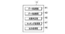
- FIG. 3 is a diagram showing an example of a functional block configuration of the defect image processing apparatus 11 according to the embodiment of the present invention.
- the defect image processing apparatus 11 includes a data acquisition unit 41, a data conversion unit 43, a defect determination unit 45, a matching processing unit 47, and an output processing unit 49.
- the data acquisition unit 41 acquires the defect data 17 from the defect data management device 7 and the layout data 23 from the design database server 9 via the network 10.
- the data conversion unit 43 converts the defect data 17 acquired from the defect data management device 7 and the layout data 23 acquired from the design database server 9 into a data format that can be used by the defect determination unit 45 and the matching processing unit 47 described later. .
- the defect determination unit 45 determines from the acquired defect data 17 whether the defect is a random defect or a systematic defect.
- the random defect is a defect caused by dust or foreign matter.
- the matching processing unit 47 aligns the origin of the defect image included in the defect data 17 and the layout data, adjusts the magnification, aligns the coordinate axes, and performs image matching.
- the output processing unit 49 outputs the defect image converted by the data conversion unit 43, the layout image based on the layout data 23, the matching processing result by the matching processing unit 47, the defect position, the category classification result, and the like to the output unit 34.
- each functional block is realized by the control unit 31 reading and executing a predetermined processing program stored in advance in the storage unit 32.
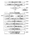
- FIG. 4 is a flowchart illustrating an example of a procedure for matching a defect image and a layout image.
- the data acquisition unit 41 first acquires the layout data 23 from the design database server 9 via the network 10 (step S101), and acquires the defect data 17 from the defect data management device 7 (step S101). S102).
- the acquired layout data 23 and defect data 17 are converted by the data converter 43 into a data format that can be read by the matching processor 47.
- the matching processing unit 47 associates one or a plurality of layers on the layout data 23 to be subjected to image matching as a matching target layer with respect to the inspection target layer on the process including the defect. That is, the matching processing unit 47 associates the layer name, the layer number, and the layer type of the layer on the layout data 23 to be matched with the inspection target layer in the process (step S103).
- This association process includes an input process from the input unit 33 by the operator, a preset recipe data reading process, and the like, and a detailed description thereof will be omitted.
- the operator can handle the layer on the layout data 23 to be matched by the name of the layer to be inspected in the process. It becomes possible to perform defect factor analysis and the like using the displayed image without being conscious of the layer number and layer type.
- the matching processing unit 47 performs origin matching between the layout data 23 and the defect data 17 (step S104).
- the origin of the coordinate system of the data representing the position may be provided at the center of the die (also referred to as a chip).
- the origin of the coordinate system of the data representing the position may be provided at the lower left corner of the die. In such a case, the origin and coordinate axes of both are made coincident so that the same position information can be represented by the same data between the two.
- the origin alignment with the defect data 17 is performed using the layout data 23 of one layer, the origin alignment with the layout data 23 of another layer does not need to be performed thereafter.
- the matching processing unit 47 for each defect included in the defect data 17, the layout image of the matching target layer obtained from the layout data 23 corresponding to the position of the defect, and the defect image stored in the image file 19. Are matched (step S105).
- the data of the coordinate position includes an error at the time of defect detection, and there are many cases where a slight misalignment occurs between the layout image and the defect image. Therefore, here, pattern matching is performed between the layout image and the defect image in a range wider than the field of view of the defect image.
- the matching processing unit 47 adjusts the magnification of the image before matching the image.
- the magnification of the defect image is a magnification when the defect image is acquired by the defect inspection apparatus 3 or the review apparatus 5, and is stored in the image information file 20 (see FIG. 2). Therefore, the matching processing unit 47 refers to the magnification included in the image information file 20 of the defect data 17, calculates the magnification for superimposing the defect image on the layout image obtained from the layout data 23, and sets the coordinate system of both images. Matching can be performed in the same way.
- the defect image data (image file 19) and its magnification (image information file 20) are associated with each other from the defect inspection apparatus 3 or the review apparatus 5 and have already been sent.
- the matching processing unit 47 can generate a layout image having the same magnification as that of the defect image without receiving input of magnification information from the operator, and can perform image matching.
- the operator does not have to worry about the magnification of the defect image to be matched, and accordingly, it can be said that the usability of the defect image processing apparatus 11 is improved for the operator.
- the matching processing unit 47 superimposes the defect image on the layout image of another layer above or below the matching target layer (step S106). That is, the matching processing unit 47 acquires a layout image of the same region portion as the defect image of a layer different from the layer including the defect from the layout data 23, and superimposes the acquired layout image on the defect image.
- the output processing unit 49 superimposes the layout image of the matching target layer and other layers above or below it and the defect image, and displays them on the output unit 34 (step S107). At this time, a plurality of other layers to be displayed can be selected.
- the operator can appropriately select, collate, and display a layout image of another layer that can cause a defect in the upper layer or the lower layer of the layer including the defect. It is possible to confirm the presence or absence of the influence of other layers on.
- the inspection target layer is a Poly-Si layer
- information such as whether the lower layer of the defect is an N-type or P-type active region (impurity implantation region) or an inactive region Therefore, based on the information, it is possible to determine whether the defect corresponds to a systematic defect or not.
- floor plan layout data exists as a layer, it is possible to easily determine whether or not it is a systematic defect. That is, by comparing the position of the defect with the area of the block defined by the floor plan, whether the defect is in the memory cell area, the wiring area, the peripheral circuit area, or the dummy pattern area Or the like, and based on the result, it can be determined whether or not it corresponds to a systematic defect.
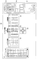
- FIG. 5 is a diagram showing an example of a screen display by the output unit 34.
- the display screen 50 displays a layer association display 51, a layout image 52, a defect image 53, a layout image & defect image 54, a wafer map display 55, a die map display 56, a defect category display 57, and the like. Is done.
- the layer association display 51 indicates the name, number, and type of the layer on the layout data 23 associated with the layer on the process including the defect performed in step S103. Even if the names of the layers are the same, the layout data 23 includes layers having different numbers and types due to differences in layer design and manufacturing processes. With the layer association display 51, the operator can appropriately select a layer on the layout data 23 to be displayed on the display screen 50.
- the layout image 52 is a so-called layout pattern image generated based on the layout data 23.
- the layout image of the matching target layer (the layer on the layout data 23 corresponding to the layer including the defect in the inspection target layer) is displayed with a solid line, and the layout image of the lower layer or the upper layer is displayed with a dotted line.
- the defect image 53 is a review image acquired by the review device 5 or the like, and is displayed based on the image file 19 included in the defect data 17.
- the layout image & defect image 54 displays the matching result between the layout image 52 and the defect image 53. That is, the layout image & defect image 54 is obtained by superimposing and displaying the result of the matching process and the layout image of another layer different from the matching target layer. It is assumed that one or a plurality of layers can be arbitrarily selected as the other layers here by an input operation of an operator or the like.
- the layout image & defect image 54 is displayed even when the matching process between the layout image and the defect image in step S105 fails.
- the layout image and the defect image are displayed slightly shifted from each other due to an error in the detection position of the defect image.
- the movement button 58 up / down / left / right button
- the wafer map display 55 represents the position of each defect included in the defect data 17 on the wafer by the dot position.
- the die map display 56 similarly represents the position of the defect in the die by the dot position.
- the floor plan data is displayed in an overlapped manner, so that it is easy to know in which block each defect is located, such as a control circuit unit, an arithmetic circuit unit, or a RAM unit in the die.
- the layout image 52 of the defect corresponding to the selected dot is displayed.
- a defect image 53 and a layout image & defect image 54 are displayed.
- the defect category display 57 shows the defect distribution by defect category classified by the ADC of the defect inspection apparatus 3. That is, in the defect category display 57, a, b, c, and d on the horizontal axis represent defect factor categories, and the vertical axis represents the occurrence frequency of defects belonging to each category.
- the defect image processing apparatus 11 includes the defect image 53, the layout image 52 of the layer that is likely to cause a defect in the upper layer and the lower layer of the layer including the defect, and the layout image & defect image 54 obtained by superimposing them. They can be displayed on the same display screen 50. Therefore, an operator who performs defect analysis can easily estimate whether or not another layer has an influence on the defect by looking at the display screen 50, and as a result, the cause of the defect can be easily analyzed. Become.
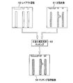
- FIG. 6 is a diagram showing an outline of matching processing in the defect image processing apparatus 11.
- the matching processing unit 47 performs automatic matching between the defect image 61 and the layout image 62 by the known normalized cross-correlation matching 63 and outputs a matching processing result 64. In this case, matching may not succeed due to the influence of the position detection error, so that the search range of the layout image 62 is set wider than the range of the defect image 61 and matching processing with the defect image 61 is performed. To do.
- the search range can be arbitrarily set by an operator's operation.
- the layer of the layout image to be matched in the matching processing unit 47 is, in principle, one layer.
- the pattern of the lower element isolation layer is also visible at the same time.
- the Poly ⁇ ⁇ Si layer acquired image (defect image 61) by the review device 5 or the like includes the element isolation layer image. Therefore, in such a case, an image obtained by superimposing the layout image of the Poly Si layer on the layout image of the element isolation layer is used as the layout image to be matched.
- the probability that the matching between the image portion other than the defect area of the defect image 61 and the layout image 62 is successful is high.
- the proportion of the defect area is large with respect to the entire area of the defect image 61, the defect area itself becomes a matching failure and often fails in matching. Therefore, here, the probability of successful matching is increased by the following matching method.
- the review device 5 usually acquires a low-magnification review image of a certain area, compares the review image with, for example, a reference image acquired in the same area of an adjacent die, and the difference
- a high-magnification review image of an area including the defective portion is acquired.
- ADC ADC-based digital converter
- a low-magnification defect image a reference image
- a high-magnification defect image a reference image
- a reference image a high-magnification defect image
- a reference image a high-magnification defect image
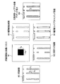
- FIG. 7 is a diagram showing an example of a matching processing method when a reference image is obtained by the defect image processing apparatus 11.
- the defect image processing apparatus 11 acquires the high-magnification defect image 80 acquired by the review apparatus 5, the reference image 81, and the image information file 20 for each image from the defect data management apparatus 7.
- the matching processing unit 47 obtains a defect area extraction image 82 by obtaining a difference between the defect image 80 and the reference image 81. Next, the matching processing unit 47 sets an image obtained by removing the defect area extraction image 82 portion from the defect image 80, that is, an image obtained by masking the defect area extraction image 82 portion of the defect image 80 as the defect mask image 83. Further, a contour line is extracted from the defect mask image 83 to obtain a contour line extraction result 84.
- the matching processing unit 47 acquires the contour line extraction result / layout matching image 85 according to the matching method shown in FIG. 6, and based on the result, the output processing unit 49 superimposes the defect image and the layout image.
- the defect image / layout image matching display 86 displayed together is output to the output unit 34.
- the low-magnification defect image obtained by the review device 5 and the low-magnification reference image are used to explain in FIG.
- a matching process may be performed by performing a process similar to the above-described process.
- FIG. 8 is a diagram illustrating an example of a matching processing method when the defect image processing apparatus 11 cannot obtain the reference image 81.
- An image information file 20 is attached to the image file 19 obtained from the defect inspection apparatus 3 or the review apparatus 5 (see FIG. 1), and the image information file 20 usually has the center of gravity of the defect included in the image file 19. Coordinate and defect size information is included. Therefore, as shown in FIG. 8, in the high-magnification defect image 80, when the defect area is a rectangular area of horizontal X D and vertical Y D , the matching processing unit 47 performs horizontal X M (> X D ), vertical A rectangular area of Y M (> Y D ) is generated and used as a defect area extraction image 91.
- the matching processing unit 47 removes the defect area extraction image 91 from the defect image 80, that is, an image obtained by masking the defect area extraction image 91 portion of the defect image 80.
- a defect mask image 92 is assumed. Further, a contour line is extracted from the defect mask image 92 to obtain a contour line extraction result 93.
- the matching processing unit 47 acquires the contour line extraction result / layout matching image 94 according to the matching method shown in FIG. 6, and based on the result, the output processing unit 49 superimposes the defect image and the layout image.
- the defect image / layout image matching display 86 displayed in this manner is output to the output unit 34.
- the defect area extraction image 91 used as a mask is rectangular, but it may be circular or elliptical, and is not limited to rectangular. If the defect area is a large defect that occupies most of the entire defect image, the same process as described with reference to FIG. 8 is performed using the low-magnification defect image obtained by the review device 5. And matching processing may be performed.
- FIG. 9 is a diagram showing an example of a systematic defect classification procedure using the defect image processing apparatus 11.
- the data acquisition unit 41 of the defect image processing apparatus 11 first acquires the defect data 17 from the defect data management apparatus 7 and acquires the ADC classification data obtained from the review apparatus 5 (step S201). And the defect determination part 45 selects the category of a random defect from the ADC classification
- step S203 If it is determined that the defect is a random defect (“Yes” in step S203), the defect is excluded from the systematic defect classification target (step S204). If it is determined that the defect is not a random defect (“No” in step S203), it is determined that the defect is a systematic defect, and systematic defect classification is started (step S205).
- the defect image processing apparatus 11 executes the same processes of steps S101 to S107 as the process described with reference to FIG. 4, and displays the display screen 50 shown in FIG. Therefore, the operator who performs the defect analysis classifies systematic defects based on the layout image & defect image 54 displayed on the display screen 50 (step S206).
- the operator compares the defect portion (defect region) of the defect displayed in the layout image & defect image 54 with the layout image of the other layer above or below the layer including the defect. It is determined whether or not it is a systematic defect based on the positional relationship and the like, and the systematic defect is further classified.
- the defect image processing device 11 automatically classifies the defect. It can be carried out. In that case, the defect image processing apparatus 11 can be said to be a semiconductor defect classification apparatus.
- a defect region of the defect is a significant region of another layer (a significant region is a region where impurities are formed, a gate material, The defect in the central part of the region where the wiring is formed, the region where the contact hole is formed, etc.) corresponds to the first type systematic defect, and the defect in the peripheral part of the significant region is A defect that falls under the second type of systematic defect and is outside a significant area is determined as not corresponding to a systematic defect.
- defects determined as random defects based on the ADC result are excluded in advance, and defects that are not random defects are also excluded.
- the defect image 53 is matched with the layout image 52 of the layer including the defect and another layer above or below it, and a layout image & defect image 54 generated by superposition is displayed on the display screen. Therefore, the operator can easily determine and classify the systematic defect and improve the work efficiency.
- image matching with a layout image can be performed using a high-magnification defect image.
- the probability of failure is reduced, and as a result, the efficiency of image matching is improved.
- an overlay image with the layout image of the other layer is displayed, which can be used to classify systematic defects that are affected by the design and manufacturing process of other layers. This makes it possible to improve the efficiency of defect factor analysis.
Landscapes
- Engineering & Computer Science (AREA)
- Physics & Mathematics (AREA)
- General Physics & Mathematics (AREA)
- Computer Vision & Pattern Recognition (AREA)
- Theoretical Computer Science (AREA)
- Quality & Reliability (AREA)
- Chemical & Material Sciences (AREA)
- Life Sciences & Earth Sciences (AREA)
- Health & Medical Sciences (AREA)
- Analytical Chemistry (AREA)
- Biochemistry (AREA)
- General Health & Medical Sciences (AREA)
- Immunology (AREA)
- Pathology (AREA)
- Testing Or Measuring Of Semiconductors Or The Like (AREA)
- Image Processing (AREA)
- Image Analysis (AREA)
- Analysing Materials By The Use Of Radiation (AREA)
- Investigating Materials By The Use Of Optical Means Adapted For Particular Applications (AREA)
Abstract
欠陥画像処理装置は、設計データから得られるレイアウト画像(52)と、欠陥画像(53)から欠陥領域部分を除去した画像と、を正規化相互相関により画像マッチングし、そのマッチング結果として、レイアウト画像&欠陥画像(54)を表示装置に表示する。このとき、レイアウト画像&欠陥画像(54)には、欠陥画像(53)と同じレイヤのレイアウト画像だけでなく、他のレイヤのレイアウト画像が欠陥画像(53)に重ね合わせて表示される。従って、他のレイヤとの位置関係で発生するシステマティック欠陥の要因解析が容易になる。
Description
本発明は、半導体デバイス製造過程で生じるウェハまたはチップにおける欠陥の検査装置から取得した欠陥画像に対する画像処理技術およびその画像処理技術を用いた半導体欠陥分類技術に関する。
近年、半導体ウェハの欠陥検査装置としては、暗視野(DF:Dark Field)欠陥検査装置、明視野(BF:Bright Field)欠陥検査装置、電子ビーム(EB:Electron Beam)欠陥検査装置など様々なものが開発され、それらを用いた欠陥検査方法も微細化対応への進歩を遂げている。例えば、これらの欠陥検査装置で検出した欠陥位置情報をもとにレビュー装置で欠陥の鮮明な画像取得を行い、その取得した画像から、欠陥を分類するADC(Automatic Defect Classification:自動欠陥分類)が行われ、欠陥カテゴリが自動的に分類される。
これまでは半導体デバイスの製造歩留まり低下の原因は、主に異物や不純物のようなランダムに発生する欠陥とされ、欠陥検査装置や欠陥レビュー装置でその要因を探り、製造工程に対策を施すことで歩留まりを維持していた。しかし、最近の半導体デバイスのパターン最小線幅は、すでに65nmを割り込み、さらに45nm、32nmへと微細化が進展している。それに伴い、ランダム欠陥に代わって、設計レイアウトに依存して発生する欠陥の比率が高まってきている。
この設計レイアウトに依存する欠陥は、システマティック欠陥と呼ばれており、製品投入時の初期段階において大量の不良を作り込んでしまうことがある。例えば、特定の形状の配線がその近隣の配線のパターンの影響を受けて、細くなったり、隣接配線とショートし易くなったりすることがある。また、下層の不純物拡散層の形状によっては、コンタクトホールにおける酸化膜のエッチング不足が生じ、上層の配線層と下層の拡散層とが電気的に接続されない場合もある。そのため、システマティック欠陥の対策には、その要因を分析して、設計データや製造プロセス条件の両方の面からの検討が必要となる。
このようなシステマティック欠陥の要因を検討・分析するためには、欠陥位置と、設計データであるレイアウトパターンと、の関係を分析する必要がある。例えば、特許文献1では、欠陥要因の解析を行うため、欠陥を含むレビュー画像とレイアウトパターンとの対応付けを行い、例えば、欠陥が生じた位置が属する領域の欠陥密度情報などによりシステマティック欠陥判定を行う方法が開示されている。
欠陥位置とレイアウトパターンとの位置関係を分析するためには、レビュー画像とレイアウトパターンとを高精度に、効率よく対応付ける必要がある。特許文献1には、半導体デバイスチップの周辺部の特徴的な形状部分に着目して、レビュー画像とレイアウトパターンとの対応付ける方法について記載されているが、大きな倍率でのレビュー画像における具体的な画像のマッチング方法についての記載はない。
そこで、本発明においては、欠陥を含むレビュー画像(以下、欠陥画像という)と設計データに基づくレイアウトパターン(以下、レイアウト画像という)画像との画像マッチングの高精度化および高効率化を図ることが可能な欠陥画像処理装置、欠陥画像処理方法、半導体欠陥分類装置および半導体欠陥分類方法を提供することを目的とする。
前記した目的を達成するために、本発明は、半導体デバイスの欠陥検査装置または欠陥レビュー装置によって取得された前記半導体デバイスの欠陥を含む部分の欠陥画像と、前記半導体デバイスのレイアウトデータから生成され、前記欠陥を含むレイヤと同じレイヤで前記欠陥画像の領域に対応した領域のレイアウト画像と、の画像マッチングを行うマッチング処理部と、前記マッチング処理部によってマッチングされた前記欠陥画像と前記レイアウト画像とを重ね合わせて表示装置に表示する出力処理部と、を備えた欠陥画像処理装置であって、前記マッチング処理部は、前記欠陥画像と前記レイアウト画像との画像マッチングを行うとき、前記欠陥画像から欠陥部分の領域の画像を除去し、前記欠陥部分の領域の画像を除去した欠陥画像と前記レイアウト画像との間で画像マッチングを行うことを特徴とする。
本発明では、欠陥画像とレイアウト画像との画像マッチングを行うとき、欠陥画像の欠陥画像部分を除去してから、その画像マッチングを行う。従って、大きな倍率の欠陥画像に欠陥部分が存在した場合であっても、画像マッチングに失敗するが少なくなくなるので、画像マッチングに失敗する確率が小さくなり、画像マッチングの効率向上を図ることができる。
欠陥レビュー装置などで取得された欠陥画像と設計データに基づくレイアウト画像とのマッチング処理の効率向上を図ることができる。
以下に、添付図面を参照しながら、本発明に係る欠陥画像処理装置および欠陥画像処理方法の好適な実施形態について詳細に説明する。なお、以下の説明および添付図面において、略同一の機能構成を有する構成要素については、同一の符号を付することにより、重複説明を省略することにする。
図1は、本発明の実施の形態に係る欠陥画像処理装置を含む半導体検査システムの構成の一例を示した図である。図1に示すように、半導体検査システム1は、欠陥検査装置3、レビュー装置5、欠陥データ管理装置7、設計データベースサーバ9、欠陥画像処理装置11などから構成される。欠陥検査装置3、レビュー装置5、欠陥データ管理装置7、設計データベースサーバ9、欠陥画像処理装置11は、ネットワーク10によってデータ送受信可能に接続される。
半導体製造工程は、不純物注入、成膜、エッチングなど様々な工程(図示省略)によって構成され、微細加工の必要性から、清浄な環境に保たれたクリーンルーム8内に構築される。そして、各工程で加工された半導体ウェハの欠陥の状況を検査する欠陥検査装置3やレビュー装置5は、そのクリーンルーム8内に設置される。
欠陥検査装置3は、製造途上にある半導体ウェハの欠陥の検出を行う、暗視野欠陥検査装置、明視野欠陥検査装置、電子ビーム欠陥検査装置などであり、被検査デバイスの表面に発生した欠陥を検出する。また、欠陥検査装置3は、検出した欠陥の観察画像(レビュー画像または欠陥画像という)を取得する機能を備える。
レビュー装置5は、走査型電子顕微鏡(SEM:Scanning Electron Microscope)などであり、欠陥検査装置3が検出した欠陥の半導体ウェハ上の座標情報を基に、欠陥の詳細なレビュー画像を取得する。レビュー装置5は、また、検出した欠陥について、その欠陥要因のカテゴリを分類するADC機能を備える。
欠陥データ管理装置7は、欠陥検査装置3やレビュー装置5によって取得され、送信される半導体ウェハの欠陥に係る各種データを、ネットワーク10を介して受信し、欠陥データ17として蓄積・管理する。ここで、ここで、欠陥データ17としては、欠陥データファイル18、画像ファイル19、画像情報ファイル20などが含まれる。
欠陥データファイル18は、欠陥検査装置3により検出された欠陥を識別する欠陥識別番号、当該欠陥の位置を各々のダイ(チップ)に設けられた所定の基準点(原点)に対して決定されたダイ上の座標系で表された欠陥位置座標、欠陥サイズ、欠陥要因のカテゴリなどの欠陥データを記憶するファイルである。
画像ファイル19は、レビュー機能を備えた欠陥検査装置3またはレビュー装置5によって取得された欠陥画像(レビュー画像)のデータを記憶するファイルである。
画像情報ファイル20は、各画像ファイル19に対応付けられて作成され、各画像ファイル19の取得状況を示す情報を記憶するファイルである。画像情報ファイル20は、図2にその一例を示すように、画像ファイル19に含まれる欠陥画像の画像倍率(低倍率、高倍率)、画像解像度(低倍率、高倍率)、欠陥を含む欠陥領域座標、欠陥領域重心座標、重ね合わせて当該画像を構成するフレーム画像の枚数など情報により構成される。
ここで、欠陥画像の画像倍率は、欠陥検査装置3またはレビュー装置5によって欠陥画像が取得されたときの欠陥画像の倍率である。その欠陥画像の倍率は、通常、半導体デバイスのデザインルールで定められたパターンの最小寸法、半導体デバイスの製造歩留まりに影響を与える欠陥に大きさ(欠陥サイズ)、その欠陥を視野に収めることができる倍率(FOV:Field Of View)などに基づき定められる。
設計データベースサーバ9は、所定の半導体製造工程で製造される半導体ウェハに形成される半導体デバイス(集積回路チップなど)のレイアウトデータ23を、半導体デバイスごとに蓄積し、管理する。レイアウトデータ23は、その半導体デバイスを構成する素子や配線などの物理的な配置に関する設計データであり、また、各製造工程で用いられるマスクの形状(マスクパターン)を定めるデータである。
欠陥画像処理装置11は、欠陥データ管理装置7から検査対象の半導体ウェハの欠陥画像を取得し、また、設計データベースサーバ9からその半導体ウェハに形成される素子や配線のレイアウト画像を取得し、両者の画像を比較して、その結果を、その後に行われる欠陥解析処理に供する。
欠陥画像処理装置11は、ワークステーションやパーソナルコンピュータなどのコンピュータによって構成され、通信部30、制御部31、記憶部32、入力部33、出力部34などを備える。
制御部31は、中央演算処理装置(CPU:Central Processing Unit)やマイクロプロセッサなどで構成される。制御部31は、他の各部の制御を行うとともに、後記するマッチング処理などを行う。記憶部32は、例えば、RAM(Random Access Memory)などの揮発性メモリ、フラッシュメモリなどの不揮発性メモリ、ハードディスク装置といった記憶装置からなり、後記するマッチング処理などを実行するプログラムなどを記憶するとともに、欠陥データ管理装置7や設計データベースサーバ9から送信される欠陥画像やレイアウトデータを記憶する。
通信部30は、ネットワーク10を介して、欠陥検査装置3、レビュー装置5、欠陥データ管理装置7、設計データベースサーバ9との間でデータの送受信を行う。すなわち、通信部30は、制御部31の指示のもとに、欠陥データ管理装置7から、検査対象の半導体ウェハの欠陥データに関する欠陥データファイル18、画像ファイル19、画像情報ファイル20などを取得し、また、設計データベースサーバ9から、その半導体ウェハに形成される集積回路チップのレイアウトデータ23を取得する。
入力部33は、キーボード、マウス、各種ボタンなどの入力装置からなり、また、出力部34は、LCD(Liquid Crystal Display)装置、プリンタなどの出力装置からなる。
図3は、本発明の実施の形態に係る欠陥画像処理装置11の機能ブロック構成の一例を示した図である。図3に示すように、欠陥画像処理装置11は、データ取得部41、データ変換部43、欠陥判定部45、マッチング処理部47、出力処理部49を含んで構成される。
データ取得部41は、ネットワーク10を介して、欠陥データ管理装置7から欠陥データ17を取得し、設計データベースサーバ9からレイアウトデータ23を取得する。データ変換部43は、欠陥データ管理装置7から取得した欠陥データ17および設計データベースサーバ9から取得したレイアウトデータ23を、後記する欠陥判定部45やマッチング処理部47で使用可能なデータ形式に変換する。
欠陥判定部45は、取得した欠陥データ17から、当該欠陥がランダム欠陥であるか、または、システマティック欠陥かであるか、を判定する。ここで、ランダム欠陥とは、塵埃や異物が原因で生じる欠陥である。マッチング処理部47は、欠陥データ17に含まれる欠陥画像とレイアウトデータの原点合わせ、倍率合わせを行って座標軸を合わせ、画像のマッチングを行う。出力処理部49は、データ変換部43によって変換された欠陥画像、レイアウトデータ23に基づくレイアウト画像、マッチング処理部47によるマッチング処理結果、欠陥位置、カテゴリ分類結果などを出力部34に出力する。
なお、前記の各機能ブロックの機能は、記憶部32にあらかじめ記憶されている所定の処理プログラムを、制御部31が読み出して、実行することによって実現される。
続いて、図4以降の図を参照して、欠陥画像処理装置11の動作について説明する。図4は、欠陥画像とレイアウト画像のマッチング処理の手順の一例を示したフローチャートである。
図4において、データ取得部41は、まず、ネットワーク10を介して、設計データベースサーバ9からレイアウトデータ23を取得し(ステップS101)、また、欠陥データ管理装置7から欠陥データ17を取得する(ステップS102)。取得されたレイアウトデータ23および欠陥データ17は、データ変換部43によってマッチング処理部47が読み出し可能なデータ形式に変換される。
次に、マッチング処理部47は、欠陥を含む工程上の検査対象レイヤに対し、画像マッチングの対象となるレイアウトデータ23上のレイヤの1つまたは複数のレイヤを、マッチング対象レイヤとして関連付ける。すなわち、マッチング処理部47は、工程上の検査対象レイヤに対して、マッチングするレイアウトデータ23上のレイヤのレイヤ名称、レイヤ番号、レイヤタイプの関連付けを行う(ステップS103)。
この関連付けの処理には、オペレータによる入力部33からの入力処理や、あらかじめ設定されたレシピデータの読み込み処理などが含まれるが、その詳細については説明を省略する。
なお、このような関連付けを行っておくことにより、オペレータは、工程上の検査対象のレイヤの名称によって、マッチング対象のレイアウトデータ23上のレイヤを扱うことが可能となり、また、その際には、レイヤ番号やレイヤタイプを意識せずに表示された画像を用いて欠陥要因分析などが行えるようになる。
次に、マッチング処理部47は、レイアウトデータ23と欠陥データ17との原点合わせを行う(ステップS104)。例えば、レイアウトデータ23において、位置を表すデータの座標系の原点は、ダイ(チップともいう)の中央に設けられることがある。一方、欠陥データ17において、位置を表すデータの座標系の原点は、ダイ左下隅に設けられることがある。このような場合には、両者の原点および座標軸を一致させ、両者の間で、同じ位置情報を同じデータで表すことができるようにする。
なお、1つのレイヤのレイアウトデータ23を用いて欠陥データ17との原点合わせが行われた場合には、他のレイヤのレイアウトデータ23との原点合わせは、その後、行う必要がない。
次に、マッチング処理部47は、欠陥データ17に含まれる欠陥ごとに、その欠陥の位置に対応するレイアウトデータ23から得られるマッチング対象レイヤのレイアウト画像と、画像ファイル19に記憶されている欠陥画像と、のマッチングを行う(ステップS105)。このとき、前のステップS104で原点合わせがすでに行っているので、当該欠陥の座標位置から、その座標位置に対応するレイアウト画像を容易に得ることができる。しかしながら、その座標位置のデータには欠陥検出時の誤差が含まれており、レイアウト画像と欠陥画像とは、多少の位置ずれを生じている場合が多い。そこで、ここでは、当該欠陥画像の視野よりも広い範囲で、レイアウト画像と欠陥画像との間でパターンマッチングを行う。
なお、図示を省略しているが、マッチング処理部47は、画像のマッチングを行う前に、画像の倍率合わせを行っている。このとき、欠陥画像の倍率は、欠陥検査装置3またはレビュー装置5によってその欠陥画像が取得されたときの倍率であり、画像情報ファイル20(図2参照)に記憶されている。そこで、マッチング処理部47は、欠陥データ17の画像情報ファイル20に含まれる倍率を参照し、レイアウトデータ23から得られるレイアウト画像に、欠陥画像を重ね合わせる倍率を算出し、両画像の座標系を同じにしてマッチングを行うことができる。
本実施形態の欠陥画像処理装置11では、欠陥検査装置3またはレビュー装置5から、欠陥画像データ(画像ファイル19)とその倍率(画像情報ファイル20)とが互いに対応付けられて、すでに送付されている(図2参照)ので、マッチング処理部47は、オペテータから倍率情報の入力を受けることなく、欠陥画像と同じ倍率のレイアウト画像を生成し、画像のマッチングを行うことができる。その結果、オペレータは、マッチング対象の欠陥画像の倍率を気にする必要がなくなり、その分、オペレータにとってみれば、欠陥画像処理装置11の使い勝手が向上したといえる。
次に、マッチング処理部47は、当該欠陥画像をマッチング対象レイヤの上層または下層の他のレイヤのレイアウト画像と重ね合わせる(ステップS106)。すなわち、マッチング処理部47は、レイアウトデータ23から当該欠陥が含まれるレイヤとは異なるレイヤの当該欠陥画像と同じ領域部分のレイアウト画像を取得し、その取得したレイアウト画像を欠陥画像に重ね合わせる。
次に、出力処理部49は、マッチング処理の結果として、マッチング対象レイヤおよびその上層または下層の他のレイヤのレイアウト画像と欠陥画像とを重ね合わせて、出力部34に表示する(ステップS107)。なお、このとき、表示する他のレイヤは複数選択可能であるとする。
このように、当該欠陥を含むレイヤの上層または下層のレイヤで、欠陥要因となり得る他のレイヤのレイアウト画像を、適宜、選択し、照合し、表示できるようにしたことによって、オペレータは、当該欠陥に対する他のレイヤの影響の有無を確認することが可能になる。例えば、検査対象レイヤがPoly-Siレイヤであった場合、当該欠陥の下層が、N型またはP型のアクティブ領域(不純物注入領域)であるのか、または、非アクティブ領域であるのか、などの情報が得ることができるので、その情報に基づき、当該欠陥がシステマティック欠陥に該当するのか、あるいは、該当しないのか、などを判断することが可能になる。
また、レイヤとして、フロアプランのレイアウトデータが存在する場合には、システマティック欠陥であるか否かの判定を簡易的に行うことができる。すなわち、欠陥の位置をフロアプランで定義されるブロックの領域と比較することによって、当該欠陥が、メモリセル領域にあるのか、配線領域にあるのか、周辺回路領域にあるのか、ダミーパターン領域にあるのか、などを判定し、その結果に基づき、システマティック欠陥に該当するのか否かを判断することができる。
図5は、出力部34による画面表示の一例を示した図である。図5に示すように、表示画面50には、レイヤ関連付け表示51、レイアウト画像52、欠陥画像53、レイアウト画像&欠陥画像54、ウェハマップ表示55、ダイマップ表示56、欠陥カテゴリ表示57などが表示される。
レイヤ関連付け表示51は、ステップS103で行われた欠陥を含む工程上のレイヤに関連付けられたレイアウトデータ23上のレイヤの名称、番号、タイプを示す。なお、同じレイヤの名称であっても、レイアウトデータ23の中には、レイヤの設計や製造工程の違いにより、番号やタイプが異なるレイヤがある。レイヤ関連付け表示51により、オペレータは、表示画面50上に表示させるレイアウトデータ23上のレイヤを、適宜、選択することができる。
レイアウト画像52は、レイアウトデータ23に基づき生成された、いわゆる、レイアウトパターンの画像である。図5では、マッチング対象レイヤ(検査対象のレイヤで、欠陥が含まれるレイヤに対応するレイアウトデータ23上のレイヤ)のレイアウト画像は、実線で、その下層または上層のレイアウト画像は、点線で表示されている。また、欠陥画像53は、レビュー装置5などによって取得されたレビュー画像であり、欠陥データ17に含まれる画像ファイル19を基に表示される。
レイアウト画像&欠陥画像54は、レイアウト画像52と欠陥画像53のマッチング結果を表示したものである。すなわち、レイアウト画像&欠陥画像54は、マッチング処理の結果と、マッチング対象レイヤと異なる他のレイヤのレイアウト画像を重ねて表示したものである。なお、ここでいう他のレイヤは、オペレータの入力操作などにより、1つまたは複数のレイヤを任意に選択可能であるとする。
レイアウト画像&欠陥画像54は、ステップS105におけるレイアウト画像と欠陥画像とのマッチング処理に失敗したときでも表示される。その場合には、レイアウト画像と欠陥画像とは、欠陥画像の検出位置の誤差のために、互いにややずれて表示されることになるので、その場合には、移動用ボタン58(上下左右ボタン)をマウスなどでクリックして、手動でレイアウト画像を移動させて重ね合わせることも可能である。
ウェハマップ表示55は、欠陥データ17に含まれる各欠陥のウェハ上の位置を、ドットの位置で表したものである。また、ダイマップ表示56は、その欠陥のダイ内での位置を、同様にドットの位置で表したものである。ダイマップ表示56では、フロアプランのデータが重ね合わせて表示されるので、各欠陥がダイ内の制御回路部、演算回路部、RAM部など、どのブロックに位置するか容易に分る。
また、表示画面50においては、オペレータがウェハマップ表示55またはダイマップ表示56に表示されたドットの1つをマウスなどで選択してクリックすると、その選択したドットに対応する欠陥のレイアウト画像52、欠陥画像53およびレイアウト画像&欠陥画像54が表示される。
欠陥カテゴリ表示57は、欠陥検査装置3のADCによって分類された欠陥要因のカテゴリ別欠陥分布を示したものである。すなわち、欠陥カテゴリ表示57において、横軸のa,b,c,dは、欠陥要因のカテゴリを表し、縦軸は、各カテゴリに属する欠陥の発生頻度を表している。
このように、欠陥画像処理装置11は、欠陥画像53と、欠陥を含むレイヤの上層や下層の欠陥要因となりそうなレイヤのレイアウト画像52と、それらを重ね合わせたレイアウト画像&欠陥画像54を、同じ表示画面50上に表示することができる。従って、欠陥解析を行うオペレータは、表示画面50を見ることによって、当該欠陥に他のレイヤが影響を及ぼしているか否かを推定することが容易になり、その結果、欠陥要因の解析が容易になる。
続いて、図6~図8を参照して、欠陥画像処理装置11において行われるマッチング処理の詳細について説明する。図6は、欠陥画像処理装置11におけるマッチング処理の概要を示した図である。
前記したように、レビュー装置5などで取得された欠陥画像61とレイアウトデータ23を基に生成されたレイアウト画像62との間には、レビュー装置5などの位置検出誤差などのためにずれが生じている場合が多い。
マッチング処理部47は、公知の正規化相互相関マッチング63により、欠陥画像61とレイアウト画像62との自動マッチングを行い、マッチング処理結果64を出力する。その場合、前記の位置検出誤差の影響により、マッチングに成功しない場合もあるため、レイアウト画像62の探索範囲を欠陥画像61の範囲よりも広く設定し、欠陥画像61とのマッチング処理を行うようにする。なお、探索範囲は、オペレータの操作により任意に設定可能である。
なお、このマッチング処理部47におけるマッチング処理対象のレイアウト画像のレイヤは、原則として1つのレイヤではある。しかしながら、レビュー装置5などで、例えば、Poly Siレイヤを見た場合、下層の素子分離レイヤのパターンも同時に見えてしまう。すなわち、レビュー装置5などによるPoly Siレイヤの取得画像(欠陥画像61)には、素子分離レイヤの画像も含まれることになる。そこで、このような場合には、マッチング処理対象のレイアウト画像として、素子分離レイヤのレイアウト画像の上にPoly Siレイヤのレイアウト画像を重ね合わせた画像を利用する。
また、このマッチング処理においては、欠陥画像61の全域に対し、欠陥領域の占める割合が小さい場合には、欠陥画像61の欠陥領域以外の画像部分とレイアウト画像62とのマッチングは成功する確率が大きい。一方、欠陥画像61の全域に対し、欠陥領域の占める割合が大きく場合には、欠陥領域自体がマッチングの障害となりマッチングに失敗することが多くなる。そこで、ここでは、以下に示すマッチング方法により、マッチング成功の確率を高める。
ところで、レビュー装置5(図1参照)は、通常、ある領域の低倍率のレビュー画像を取得し、そのレビュー画像を、例えば、隣接するダイの同じ領域で取得した参照画像と比較し、その差分画像により欠陥の有無を検出し、欠陥を検出した場合には、その欠陥部分を含む領域の高倍率のレビュー画像を取得している。また、ADCを行う場合には、そのADCによる分類精度を向上させるために、高倍率の参照画像を用いている。
このように、レビュー装置5からは、低倍率の欠陥画像、参照画像、高倍率の欠陥画像、参照画像の4種類のレビュー画像が取得される。以下、高倍率の画像を用いてマッチング処理を行う場合について説明する。なお、高倍率のレビュー画像がない場合には、低倍率のレビュー画像から欠陥部分を含んだ領域を切り出し、拡大して、高倍率のレビュー画像(欠陥画像または参照画像)としてもよい。
図7は、欠陥画像処理装置11で参照画像が得られる場合のマッチング処理方法の一例を示した図である。
欠陥画像処理装置11は、レビュー装置5が取得した高倍率の欠陥画像80と、参照画像81と、それぞれの画像に対する画像情報ファイル20と、を欠陥データ管理装置7から取得する。
マッチング処理部47は、欠陥画像80と参照画像81との差分を求めて欠陥領域抽出画像82を得る。次に、マッチング処理部47は、欠陥画像80から欠陥領域抽出画像82部分を除去した画像、すなわち、欠陥画像80のうち欠陥領域抽出画像82部分をマスクした画像を、欠陥マスク画像83とする。さらに、欠陥マスク画像83から輪郭線を抽出し、輪郭線抽出結果84を得る。
続いて、マッチング処理部47は、図6で示したマッチング手法に従って、輪郭線抽出結果・レイアウトマッチング画像85を取得し、その結果に基づき、出力処理部49は、欠陥画像とレイアウト画像とを重ね合わせて表示した欠陥画像・レイアウト画像マッチング表示86を出力部34に出力する。
また、欠陥領域が欠陥画像全域の大部分を占めるような大きな欠陥である場合には、レビュー装置5で得られた低倍率の欠陥画像と低倍率の参照画像とを用いて、図7で説明した処理と同様の処理を行い、マッチング処理を行ってもよい。
次に、参照画像81が得られない場合のマッチング処理について説明する。図8は、欠陥画像処理装置11で参照画像81が得られない場合のマッチング処理方法の一例を示した図である。
欠陥検査装置3またはレビュー装置5から得られる画像ファイル19には、画像情報ファイル20が付属し(図1参照)、画像情報ファイル20には、通常、その、画像ファイル19に含まれる欠陥の重心座標および欠陥サイズの情報が含まれている。そこで、図8に示すように、高倍率の欠陥画像80において、欠陥領域が横XD、縦YDの矩形領域である場合、マッチング処理部47は、横XM(>XD)、縦YM(>YD)の矩形領域を生成し、欠陥領域抽出画像91とする。
以下、図7の場合と同様にして、マッチング処理部47は、欠陥画像80から欠陥領域抽出画像91を除去した画像、すなわち、欠陥画像80のうち欠陥領域抽出画像91部分をマスクした画像を、欠陥マスク画像92とする。さらに、欠陥マスク画像92から輪郭線を抽出し、輪郭線抽出結果93を得る。
さらに、マッチング処理部47は、図6で示したマッチング手法に従って、輪郭線抽出結果・レイアウトマッチング画像94を取得し、その結果に基づき、出力処理部49は、欠陥画像とレイアウト画像とを重ね合わせて表示した欠陥画像・レイアウト画像マッチング表示86を出力部34に出力する。
なお、ここでは、マスクとして用いる欠陥領域抽出画像91は、矩形であるとしたが、円形や楕円形などであってもよく、矩形に限定されるものではない。また、欠陥領域が欠陥画像全域の大部分を占めるような大きな欠陥である場合には、レビュー装置5で得られた低倍率の欠陥画像を用いて、図8で説明した処理と同様の処理を行い、マッチング処理を行ってもよい。
以上、図7または図8を用いて説明した画像マッチング方法を用いると、欠陥を含むレビュー画像(欠陥画像)であっても、その領域に対応する(欠陥のない)レイアウト画像との画像マッチングで失敗する確率を低減させることが可能になる。
図9は、欠陥画像処理装置11を用いたシステマティック欠陥分類の手順の一例を示した図である。
欠陥画像処理装置11のデータ取得部41は、まず、欠陥データ管理装置7から欠陥データ17を取得し、レビュー装置5から得られたADC分類データを取得する(ステップS201)。そして、欠陥判定部45は、そのADC分類データから、ランダム欠陥のカテゴリを選択し(ステップS202)、欠陥データ17に含まれる各欠陥について、その欠陥がランダム欠陥であるか否かを判定する(ステップS203)。
そして、その判定の結果、その欠陥がランダム欠陥であると判定された場合には(ステップS203で「Yes」)、その欠陥はシステマティック欠陥分類の対象外とする(ステップS204)。また、その欠陥がランダム欠陥でないと判定された場合には(ステップS203で「No」)、当該欠陥はシステマティック欠陥であるとして、システマティック欠陥の分類を開始する(ステップS205)。
その後、欠陥画像処理装置11は、図4で説明した処理と同じステップS101~S107の処理を実行し、図5に示した表示画面50を表示する。そこで、欠陥解析を行うオペレータは、表示画面50に表示されたレイアウト画像&欠陥画像54に基づき、システマティック欠陥を分類する(ステップS206)。
なお、この場合、オペレータは、レイアウト画像&欠陥画像54に表示された当該欠陥の欠陥部分(欠陥領域)と、当該欠陥を含むレイヤの上層または下層の他のレイヤのレイアウト画像と、の相対的な位置関係などに基づき、システマティック欠陥であるか否かを判定し、そのシステマティック欠陥をさらに細かく分類する。
そして、そのシステマティック欠陥であるか否かの判定やそれをさらに細かく分類する方法が、あらかじめコンピュータが判定可能なルールとして定められている場合には、欠陥画像処理装置11は、欠陥分類を自動で行うことができる。その場合には、欠陥画像処理装置11は、半導体欠陥分類装置ということができる
なお、システマティック欠陥であることを判定し、分類するルールとしては、例えば、当該欠陥の欠陥領域が、他のレイヤの有意な領域(有意な領域とは、不純物が形成される領域、ゲート材料や配線が形成される領域、コンタクトホールが形成される領域などをいう)の中央部分にある場合の欠陥は、第1種のシステマティック欠陥に該当、有意な領域の周縁部分にある場合の欠陥は、第2種のシステマティック欠陥に該当、有意な領域の外にある場合の欠陥は、システマティック欠陥に非該当などのように定めておく。
以上のように、欠陥画像処理装置11またはそれを用いた半導体欠陥分類装置においては、ADC結果に基づきランダム欠陥と判定された欠陥を事前に除外され、さらに、ランダム欠陥でない欠陥については、その欠陥の欠陥画像53と、欠陥を含むレイヤおよびその上層または下層の他のレイヤのレイアウト画像52と、がマッチングされ、重ね合わせて生成されたレイアウト画像&欠陥画像54が表示画面に表示される。従って、オペレータは、システマティック欠陥であることの判定やその分類が容易になり、その作業効率を向上させることができる。
以上説明したように、本発明の実施の形態にかかる欠陥画像処理装置11またはそれを用いた半導体欠陥分類装置によれば、高倍率の欠陥画像を用いてレイアウト画像との画像マッチングを行っても失敗する確率が低減され、その結果として画像マッチングの効率が向上する。また、欠陥画像と同じレイヤだけでなく、他のレイヤのレイアウト画像との重ね合わせ画像が表示されるため、他のレイヤの設計や製造工程に影響されて発生するシステマティック欠陥の分類に役立てることが可能となり、欠陥要因解析の効率化を図ることが可能となる。
1 半導体検査システム
3 欠陥検査装置
5 レビュー装置
7 欠陥データ管理装置
8 クリーンルーム
9 設計データベースサーバ
10 ネットワーク
11 欠陥画像処理装置
17 欠陥データ
18 欠陥データファイル
19 画像ファイル
20 画像情報ファイル
23 レイアウトデータ
30 通信部
31 制御部
32 記憶部
33 入力部
34 出力部
41 データ取得部
43 データ変換部
45 欠陥判定部
47 マッチング処理部
49 出力処理部
50 表示画面
51 レイヤ関連付け表示
52 レイアウト画像
53 欠陥画像
54 レイアウト画像&欠陥画像
55 ウェハマップ表示
56 ダイマップ表示
57 欠陥カテゴリ表示
58 移動用ボタン
3 欠陥検査装置
5 レビュー装置
7 欠陥データ管理装置
8 クリーンルーム
9 設計データベースサーバ
10 ネットワーク
11 欠陥画像処理装置
17 欠陥データ
18 欠陥データファイル
19 画像ファイル
20 画像情報ファイル
23 レイアウトデータ
30 通信部
31 制御部
32 記憶部
33 入力部
34 出力部
41 データ取得部
43 データ変換部
45 欠陥判定部
47 マッチング処理部
49 出力処理部
50 表示画面
51 レイヤ関連付け表示
52 レイアウト画像
53 欠陥画像
54 レイアウト画像&欠陥画像
55 ウェハマップ表示
56 ダイマップ表示
57 欠陥カテゴリ表示
58 移動用ボタン
Claims (13)
- 半導体デバイスの欠陥検査装置または欠陥レビュー装置によって取得された前記半導体デバイスの欠陥を含む部分の欠陥画像と、前記半導体デバイスのレイアウトデータから生成され、前記欠陥を含むレイヤと同じレイヤで前記欠陥画像の領域に対応した領域のレイアウト画像と、の画像マッチングを行うマッチング処理部と、
前記マッチング処理部によってマッチングされた前記欠陥画像と前記レイアウト画像とを重ね合わせた重ね合わせ画像を表示装置に表示する出力処理部と、
を備えた欠陥画像処理装置であって、
前記マッチング処理部は、
前記欠陥画像と前記レイアウト画像との画像マッチングを行うとき、前記欠陥画像から欠陥部分の領域の画像を除去し、前記欠陥部分の領域の画像を除去した欠陥画像と前記レイアウト画像との間で画像マッチングを行うこと
を特徴とする欠陥画像処理装置。 - 前記欠陥部分の領域は、
前記欠陥検査装置または欠陥レビュー装置によって取得された前記半導体デバイスの前記欠陥画像と同じ構造を有する他の部分のレビュー画像と、前記欠陥画像と、の差分画像として得られた領域であること
を特徴とする請求の範囲第1項に記載の欠陥画像処理装置。 - 前記欠陥部分の領域は、
前記欠陥画像に含まれる欠陥について、前記欠陥検査装置または欠陥レビュー装置によって取得された前記欠陥の位置および欠陥サイズによって定められた領域であること
を特徴とする請求の範囲第1項に記載の欠陥画像処理装置。 - 前記マッチング処理部は、
前記欠陥画像と前記レイアウト画像との画像マッチングを行うときには、前記欠陥検査装置または欠陥レビュー装置によって取得され、前記欠陥検査装置または欠陥レビュー装置から送付された欠陥画像の倍率に合わせて、前記レイアウト画像の倍率を定めること
を特徴とする請求の範囲第1項に記載の欠陥画像処理装置。 - 前記出力処理部は、
前記重ね合わせ画像を表示するとき、前記欠陥を含むレイヤと異なるレイヤで前記欠陥画像の領域に対応した領域のレイアウト画像をさらに重ね合わせて表示すること
を特徴とする請求の範囲第1項に記載の欠陥画像処理装置。 - 前記出力処理部は、
前記欠陥画像と、前記レイアウト画像と、前記重ね合わせ画像と、を前記表示装置の同じ画面内に同時に表示すること
を特徴とする請求の範囲第1項に記載の欠陥画像処理装置。 - 半導体デバイスの欠陥検査装置または欠陥レビュー装置によって取得された前記半導体デバイスの欠陥を含む部分の欠陥画像と、前記半導体デバイスのレイアウトデータから生成され、前記欠陥を含むレイヤと同じレイヤで前記欠陥画像の領域に対応した領域のレイアウト画像と、の画像マッチングを行う処理と、
前記マッチング処理部によってマッチングされた前記欠陥画像と前記レイアウト画像とを重ね合わせた重ね合わせ画像を表示装置に表示する処理と、
を実行するコンピュータによって行われる欠陥画像処理方法であって、
前記コンピュータは、
前記画像マッチングを行う処理で前記欠陥画像と前記レイアウト画像との画像マッチングを行うとき、前記欠陥画像から欠陥部分の領域の画像を除去し、前記欠陥部分の領域の画像を除去した欠陥画像と前記レイアウト画像との間で画像マッチングを行うこと
を特徴とする欠陥画像処理方法。 - 前記欠陥部分の領域は、
前記欠陥検査装置または欠陥レビュー装置によって取得された前記半導体デバイスの前記欠陥画像と同じ構造を有する他の部分のレビュー画像と、前記欠陥画像と、の差分画像として得られた領域であること
を特徴とする請求の範囲第7項に記載の欠陥画像処理方法。 - 前記欠陥部分の領域は、
前記欠陥画像に含まれる欠陥について、前記欠陥検査装置または欠陥レビュー装置によって取得された前記欠陥の位置および欠陥サイズによって定められた領域であること
を特徴とする請求の範囲第7項に記載の欠陥画像処理方法。 - 半導体デバイスの欠陥検査装置または欠陥レビュー装置によって取得された前記半導体デバイスの欠陥を含む部分の欠陥画像と、前記半導体デバイスのレイアウトデータから生成され、前記欠陥を含むレイヤと同じレイヤで前記欠陥画像の領域に対応した領域のレイアウト画像と、の画像マッチングを行うマッチング処理部と、
前記マッチング処理部によってマッチングされた前記欠陥画像と前記レイアウト画像とを重ね合わせた重ね合わせ画像を表示装置に表示する出力処理部と、
前記欠陥がレイアウト依存性を有するシステマティック欠陥であるか否かを判定する欠陥判定部と、
を備えた半導体欠陥分類装置であって、
前記マッチング処理部は、
前記欠陥画像と前記レイアウト画像との画像マッチングを行うとき、前記欠陥画像から欠陥部分の領域の画像を除去し、前記欠陥部分の領域の画像を除去した欠陥画像と前記レイアウト画像との間で画像マッチングを行い、
前記欠陥判定部は、
前記重ね合わせ画像によって得られる前記欠陥の位置と前記レイアウト画像との相対位置関係に基づき、システマティック欠陥であることを判定すること
を特徴とする半導体欠陥分類装置。 - 前記欠陥判定部は、
前記欠陥検査装置または前記欠陥レビュー装置によって取得された前記半導体デバイスの欠陥にその欠陥の分類データが付されている場合には、その分類データがランダム欠陥である欠陥をシステマティック欠陥から除外すること
を特徴とする請求の範囲第10項に記載の半導体欠陥分類装置。 - 半導体デバイスの欠陥検査装置または欠陥レビュー装置によって取得された前記半導体デバイスの欠陥を含む部分の欠陥画像と、前記半導体デバイスのレイアウトデータから生成され、前記欠陥を含むレイヤと同じレイヤで前記欠陥画像の領域に対応した領域のレイアウト画像と、の画像マッチングを行うマッチング処理部と、
前記マッチング処理部によってマッチングされた前記欠陥画像と前記レイアウト画像とを重ね合わせた重ね合わせ画像を表示装置に表示する出力処理部と、
前記欠陥がレイアウト依存性を有するシステマティック欠陥であるか否かを判定する欠陥判定部と、
を備えた半導体欠陥分類装置におけるであって、半導体欠陥分類方法であって、
前記マッチング処理部は、
前記欠陥画像と前記レイアウト画像との画像マッチングを行うとき、前記欠陥画像から欠陥部分の領域の画像を除去し、前記欠陥部分の領域の画像を除去した欠陥画像と前記レイアウト画像との間で画像マッチングを行い、
前記欠陥判定部は、
前記重ね合わせ画像によって得られる前記欠陥の位置と前記レイアウト画像との相対位置関係に基づき、システマティック欠陥であることを判定すること
を特徴とする半導体欠陥分類方法。 - 前記欠陥判定部は、
前記欠陥検査装置または前記欠陥レビュー装置によって取得された前記半導体デバイスの欠陥にその欠陥の分類データが付されている場合には、その分類データがランダム欠陥である欠陥をシステマティック欠陥から除外すること
を特徴とする請求の範囲第12項に記載の半導体欠陥分類方法。
Priority Applications (1)
| Application Number | Priority Date | Filing Date | Title |
|---|---|---|---|
| US13/375,880 US8995748B2 (en) | 2009-06-02 | 2010-06-01 | Defect image processing apparatus, defect image processing method, semiconductor defect classifying apparatus, and semiconductor defect classifying method |
Applications Claiming Priority (2)
| Application Number | Priority Date | Filing Date | Title |
|---|---|---|---|
| JP2009132888A JP5479782B2 (ja) | 2009-06-02 | 2009-06-02 | 欠陥画像処理装置、欠陥画像処理方法、半導体欠陥分類装置および半導体欠陥分類方法 |
| JP2009-132888 | 2009-06-02 |
Publications (1)
| Publication Number | Publication Date |
|---|---|
| WO2010140577A1 true WO2010140577A1 (ja) | 2010-12-09 |
Family
ID=43297711
Family Applications (1)
| Application Number | Title | Priority Date | Filing Date |
|---|---|---|---|
| PCT/JP2010/059237 Ceased WO2010140577A1 (ja) | 2009-06-02 | 2010-06-01 | 欠陥画像処理装置、欠陥画像処理方法、半導体欠陥分類装置および半導体欠陥分類方法 |
Country Status (3)
| Country | Link |
|---|---|
| US (1) | US8995748B2 (ja) |
| JP (1) | JP5479782B2 (ja) |
| WO (1) | WO2010140577A1 (ja) |
Cited By (1)
| Publication number | Priority date | Publication date | Assignee | Title |
|---|---|---|---|---|
| CN111126431A (zh) * | 2019-11-13 | 2020-05-08 | 广州供电局有限公司 | 一种基于模板匹配的海量电力缺陷照片快速筛选方法 |
Families Citing this family (20)
| Publication number | Priority date | Publication date | Assignee | Title |
|---|---|---|---|---|
| JP6078234B2 (ja) * | 2012-04-13 | 2017-02-08 | 株式会社日立ハイテクノロジーズ | 荷電粒子線装置 |
| US10483081B2 (en) * | 2014-10-22 | 2019-11-19 | Kla-Tencor Corp. | Self directed metrology and pattern classification |
| JP6771495B2 (ja) * | 2015-08-12 | 2020-10-21 | ケーエルエー コーポレイション | 設計を利用する先行層欠陥箇所の点検 |
| TWI684225B (zh) * | 2015-08-28 | 2020-02-01 | 美商克萊譚克公司 | 自定向計量和圖樣分類 |
| JP6833366B2 (ja) * | 2016-07-06 | 2021-02-24 | キヤノン株式会社 | 情報処理装置、情報処理装置の制御方法及びプログラム |
| KR101753686B1 (ko) | 2017-02-16 | 2017-07-19 | 강무성 | 회로 해석 및 검증이 가능한 시뮬레이션 시스템 |
| JP6705777B2 (ja) * | 2017-07-10 | 2020-06-03 | ファナック株式会社 | 機械学習装置、検査装置及び機械学習方法 |
| CN107464236B (zh) * | 2017-07-28 | 2020-05-05 | 武汉华星光电半导体显示技术有限公司 | 一种基于aoi的柔性显示基板缺陷判别方法 |
| JP7063165B2 (ja) | 2018-07-26 | 2022-05-09 | 富士通株式会社 | 計測装置、計測方法及び計測プログラム |
| JP7053417B2 (ja) | 2018-09-13 | 2022-04-12 | キオクシア株式会社 | 欠陥検査装置および欠陥検査方法 |
| US11475556B2 (en) | 2019-05-30 | 2022-10-18 | Bruker Nano, Inc. | Method and apparatus for rapidly classifying defects in subcomponents of manufactured component |
| US11816411B2 (en) * | 2020-01-29 | 2023-11-14 | Taiwan Semiconductor Manufacturing Co., Ltd. | Method and system for semiconductor wafer defect review |
| US11321835B2 (en) * | 2020-03-17 | 2022-05-03 | Applied Materials Israel Ltd. | Determining three dimensional information |
| JP7564865B2 (ja) * | 2020-04-01 | 2024-10-09 | 富士フイルム株式会社 | 3次元表示装置、3次元表示方法、及びプログラム |
| JP7148657B2 (ja) * | 2021-02-24 | 2022-10-05 | 株式会社クレスコ | 情報処理装置、情報処理方法及び情報処理プログラム |
| JP7524852B2 (ja) * | 2021-07-13 | 2024-07-30 | 信越半導体株式会社 | デブリ判定方法 |
| CN113743447B (zh) * | 2021-07-15 | 2024-05-17 | 上海朋熙半导体有限公司 | 半导体瑕疵识别方法、装置、计算机设备和存储介质 |
| US12505532B2 (en) * | 2021-11-17 | 2025-12-23 | Sonix, Inc. | Method and apparatus for automated defect detection |
| US12207415B2 (en) | 2021-11-29 | 2025-01-21 | Hewlett Packard Enterprise Development Lp | Identifications of deviations relating to assemblies of components |
| JP2023168950A (ja) * | 2022-05-16 | 2023-11-29 | キヤノン株式会社 | 画像処理装置、画像処理方法およびプログラム |
Citations (3)
| Publication number | Priority date | Publication date | Assignee | Title |
|---|---|---|---|---|
| JP2005283326A (ja) * | 2004-03-30 | 2005-10-13 | Hitachi High-Technologies Corp | 欠陥レビュー方法及びその装置 |
| JP2009010286A (ja) * | 2007-06-29 | 2009-01-15 | Hitachi High-Technologies Corp | 半導体欠陥分類方法、半導体欠陥分類装置、半導体欠陥分類装置のプログラム、半導体欠陥検査方法、および、半導体欠陥検査システム |
| JP2009071136A (ja) * | 2007-09-14 | 2009-04-02 | Hitachi High-Technologies Corp | データ管理装置、検査システムおよび欠陥レビュー装置 |
Family Cites Families (4)
| Publication number | Priority date | Publication date | Assignee | Title |
|---|---|---|---|---|
| US7593565B2 (en) * | 2004-12-08 | 2009-09-22 | Rudolph Technologies, Inc. | All surface data for use in substrate inspection |
| JP4688525B2 (ja) * | 2004-09-27 | 2011-05-25 | 株式会社 日立ディスプレイズ | パターン修正装置および表示装置の製造方法 |
| US7676077B2 (en) * | 2005-11-18 | 2010-03-09 | Kla-Tencor Technologies Corp. | Methods and systems for utilizing design data in combination with inspection data |
| JP5081590B2 (ja) * | 2007-11-14 | 2012-11-28 | 株式会社日立ハイテクノロジーズ | 欠陥観察分類方法及びその装置 |
-
2009
- 2009-06-02 JP JP2009132888A patent/JP5479782B2/ja active Active
-
2010
- 2010-06-01 WO PCT/JP2010/059237 patent/WO2010140577A1/ja not_active Ceased
- 2010-06-01 US US13/375,880 patent/US8995748B2/en active Active
Patent Citations (3)
| Publication number | Priority date | Publication date | Assignee | Title |
|---|---|---|---|---|
| JP2005283326A (ja) * | 2004-03-30 | 2005-10-13 | Hitachi High-Technologies Corp | 欠陥レビュー方法及びその装置 |
| JP2009010286A (ja) * | 2007-06-29 | 2009-01-15 | Hitachi High-Technologies Corp | 半導体欠陥分類方法、半導体欠陥分類装置、半導体欠陥分類装置のプログラム、半導体欠陥検査方法、および、半導体欠陥検査システム |
| JP2009071136A (ja) * | 2007-09-14 | 2009-04-02 | Hitachi High-Technologies Corp | データ管理装置、検査システムおよび欠陥レビュー装置 |
Cited By (1)
| Publication number | Priority date | Publication date | Assignee | Title |
|---|---|---|---|---|
| CN111126431A (zh) * | 2019-11-13 | 2020-05-08 | 广州供电局有限公司 | 一种基于模板匹配的海量电力缺陷照片快速筛选方法 |
Also Published As
| Publication number | Publication date |
|---|---|
| JP5479782B2 (ja) | 2014-04-23 |
| JP2010283004A (ja) | 2010-12-16 |
| US20120141011A1 (en) | 2012-06-07 |
| US8995748B2 (en) | 2015-03-31 |
Similar Documents
| Publication | Publication Date | Title |
|---|---|---|
| JP5479782B2 (ja) | 欠陥画像処理装置、欠陥画像処理方法、半導体欠陥分類装置および半導体欠陥分類方法 | |
| JP5021503B2 (ja) | パターン欠陥解析装置、パターン欠陥解析方法およびパターン欠陥解析プログラム | |
| JP6080379B2 (ja) | 半導体欠陥分類装置及び半導体欠陥分類装置用のプログラム | |
| US8595666B2 (en) | Semiconductor defect classifying method, semiconductor defect classifying apparatus, and semiconductor defect classifying program | |
| JP3904419B2 (ja) | 検査装置および検査システム | |
| JP5444092B2 (ja) | 検査方法およびその装置 | |
| JP4791267B2 (ja) | 欠陥検査システム | |
| JP5081590B2 (ja) | 欠陥観察分類方法及びその装置 | |
| JP5357725B2 (ja) | 欠陥検査方法及び欠陥検査装置 | |
| JP2002100660A (ja) | 欠陥検出方法と欠陥観察方法及び欠陥検出装置 | |
| JP5068591B2 (ja) | 半導体欠陥分類方法、半導体欠陥分類装置、半導体欠陥分類装置のプログラム、半導体欠陥検査方法、および、半導体欠陥検査システム | |
| US20030195712A1 (en) | Inspection condition setting program, inspection device and inspection system | |
| US20140199792A1 (en) | Defect pattern evaluation method, defect pattern evaluation apparatus, and recording media | |
| US20100106447A1 (en) | Defect analyzing apparatus and defect analyzing method | |
| JP2011023638A (ja) | 検査領域設定方法 | |
| JP5323457B2 (ja) | 観察条件決定支援装置および観察条件決定支援方法 | |
| JP2013236031A (ja) | 欠陥分類装置、欠陥分類方法 | |
| JP4346537B2 (ja) | 表面検査装置および表面検査方法 | |
| JP5469704B2 (ja) | 欠陥解析装置、欠陥解析方法および欠陥解析プログラム | |
| US7855088B2 (en) | Method for manufacturing integrated circuits by guardbanding die regions | |
| US12619219B2 (en) | Fabrication fingerprint for proactive yield management | |
| US20220334567A1 (en) | Fabrication fingerprint for proactive yield management | |
| JP2004165395A (ja) | 検査データ解析プログラムと検査方法 | |
| JP2012080036A (ja) | システマティック欠陥判定方法およびその装置 |
Legal Events
| Date | Code | Title | Description |
|---|---|---|---|
| 121 | Ep: the epo has been informed by wipo that ep was designated in this application |
Ref document number: 10783360 Country of ref document: EP Kind code of ref document: A1 |
|
| NENP | Non-entry into the national phase |
Ref country code: DE |
|
| WWE | Wipo information: entry into national phase |
Ref document number: 13375880 Country of ref document: US |
|
| 122 | Ep: pct application non-entry in european phase |
Ref document number: 10783360 Country of ref document: EP Kind code of ref document: A1 |