WO2010119775A1 - 色素増感太陽電池および色素増感太陽電池モジュール - Google Patents
色素増感太陽電池および色素増感太陽電池モジュール Download PDFInfo
- Publication number
- WO2010119775A1 WO2010119775A1 PCT/JP2010/055894 JP2010055894W WO2010119775A1 WO 2010119775 A1 WO2010119775 A1 WO 2010119775A1 JP 2010055894 W JP2010055894 W JP 2010055894W WO 2010119775 A1 WO2010119775 A1 WO 2010119775A1
- Authority
- WO
- WIPO (PCT)
- Prior art keywords
- layer
- conductive layer
- solar cell
- porous
- dye
- Prior art date
Links
- 239000004065 semiconductor Substances 0.000 claims abstract description 174
- 239000003792 electrolyte Substances 0.000 claims abstract description 96
- 230000003746 surface roughness Effects 0.000 claims abstract description 96
- 230000001235 sensitizing effect Effects 0.000 claims abstract description 36
- 239000003054 catalyst Substances 0.000 claims description 97
- 239000000463 material Substances 0.000 claims description 35
- 239000007769 metal material Substances 0.000 claims description 8
- 229910044991 metal oxide Inorganic materials 0.000 claims description 8
- 150000004706 metal oxides Chemical class 0.000 claims description 8
- PXHVJJICTQNCMI-UHFFFAOYSA-N Nickel Chemical compound [Ni] PXHVJJICTQNCMI-UHFFFAOYSA-N 0.000 claims description 7
- XOLBLPGZBRYERU-UHFFFAOYSA-N tin dioxide Chemical compound O=[Sn]=O XOLBLPGZBRYERU-UHFFFAOYSA-N 0.000 claims description 7
- 229910001887 tin oxide Inorganic materials 0.000 claims description 7
- XLOMVQKBTHCTTD-UHFFFAOYSA-N Zinc monoxide Chemical compound [Zn]=O XLOMVQKBTHCTTD-UHFFFAOYSA-N 0.000 claims description 6
- 229910052719 titanium Inorganic materials 0.000 claims description 6
- 239000010936 titanium Substances 0.000 claims description 6
- RTAQQCXQSZGOHL-UHFFFAOYSA-N Titanium Chemical compound [Ti] RTAQQCXQSZGOHL-UHFFFAOYSA-N 0.000 claims description 5
- 229910052759 nickel Inorganic materials 0.000 claims description 4
- 239000002131 composite material Substances 0.000 claims description 3
- 229910003437 indium oxide Inorganic materials 0.000 claims description 3
- RHZWSUVWRRXEJF-UHFFFAOYSA-N indium tin Chemical compound [In].[Sn] RHZWSUVWRRXEJF-UHFFFAOYSA-N 0.000 claims description 3
- PJXISJQVUVHSOJ-UHFFFAOYSA-N indium(iii) oxide Chemical compound [O-2].[O-2].[O-2].[In+3].[In+3] PJXISJQVUVHSOJ-UHFFFAOYSA-N 0.000 claims description 3
- 229910052715 tantalum Inorganic materials 0.000 claims description 3
- GUVRBAGPIYLISA-UHFFFAOYSA-N tantalum atom Chemical compound [Ta] GUVRBAGPIYLISA-UHFFFAOYSA-N 0.000 claims description 3
- 239000011787 zinc oxide Substances 0.000 claims description 2
- 230000003197 catalytic effect Effects 0.000 abstract 2
- 239000000975 dye Substances 0.000 description 72
- 239000000758 substrate Substances 0.000 description 50
- 230000015572 biosynthetic process Effects 0.000 description 45
- 238000004519 manufacturing process Methods 0.000 description 42
- 239000010408 film Substances 0.000 description 38
- 238000000034 method Methods 0.000 description 34
- 239000002245 particle Substances 0.000 description 27
- 230000000052 comparative effect Effects 0.000 description 21
- 238000007789 sealing Methods 0.000 description 21
- GWEVSGVZZGPLCZ-UHFFFAOYSA-N Titan oxide Chemical compound O=[Ti]=O GWEVSGVZZGPLCZ-UHFFFAOYSA-N 0.000 description 19
- 239000011521 glass Substances 0.000 description 19
- WEVYAHXRMPXWCK-UHFFFAOYSA-N Acetonitrile Chemical compound CC#N WEVYAHXRMPXWCK-UHFFFAOYSA-N 0.000 description 18
- OGIDPMRJRNCKJF-UHFFFAOYSA-N titanium oxide Inorganic materials [Ti]=O OGIDPMRJRNCKJF-UHFFFAOYSA-N 0.000 description 16
- 238000006243 chemical reaction Methods 0.000 description 15
- 238000001179 sorption measurement Methods 0.000 description 15
- 239000010419 fine particle Substances 0.000 description 13
- 239000002904 solvent Substances 0.000 description 13
- 239000000126 substance Substances 0.000 description 13
- 238000002347 injection Methods 0.000 description 12
- 239000007924 injection Substances 0.000 description 12
- 229920005989 resin Polymers 0.000 description 12
- 239000011347 resin Substances 0.000 description 12
- 238000000576 coating method Methods 0.000 description 11
- 239000000243 solution Substances 0.000 description 11
- VZSRBBMJRBPUNF-UHFFFAOYSA-N 2-(2,3-dihydro-1H-inden-2-ylamino)-N-[3-oxo-3-(2,4,6,7-tetrahydrotriazolo[4,5-c]pyridin-5-yl)propyl]pyrimidine-5-carboxamide Chemical compound C1C(CC2=CC=CC=C12)NC1=NC=C(C=N1)C(=O)NCCC(N1CC2=C(CC1)NN=N2)=O VZSRBBMJRBPUNF-UHFFFAOYSA-N 0.000 description 10
- 239000011248 coating agent Substances 0.000 description 10
- RVTZCBVAJQQJTK-UHFFFAOYSA-N oxygen(2-);zirconium(4+) Chemical compound [O-2].[O-2].[Zr+4] RVTZCBVAJQQJTK-UHFFFAOYSA-N 0.000 description 10
- 238000007650 screen-printing Methods 0.000 description 10
- 239000005341 toughened glass Substances 0.000 description 10
- 229910001928 zirconium oxide Inorganic materials 0.000 description 10
- KJTLSVCANCCWHF-UHFFFAOYSA-N Ruthenium Chemical compound [Ru] KJTLSVCANCCWHF-UHFFFAOYSA-N 0.000 description 9
- 229910006404 SnO 2 Inorganic materials 0.000 description 9
- LFQSCWFLJHTTHZ-UHFFFAOYSA-N Ethanol Chemical compound CCO LFQSCWFLJHTTHZ-UHFFFAOYSA-N 0.000 description 8
- 230000006870 function Effects 0.000 description 8
- 150000002500 ions Chemical class 0.000 description 8
- 229910052707 ruthenium Inorganic materials 0.000 description 8
- 239000001856 Ethyl cellulose Substances 0.000 description 7
- ZZSNKZQZMQGXPY-UHFFFAOYSA-N Ethyl cellulose Chemical compound CCOCC1OC(OC)C(OCC)C(OCC)C1OC1C(O)C(O)C(OC)C(CO)O1 ZZSNKZQZMQGXPY-UHFFFAOYSA-N 0.000 description 7
- 238000001035 drying Methods 0.000 description 7
- 239000008151 electrolyte solution Substances 0.000 description 7
- 229920001249 ethyl cellulose Polymers 0.000 description 7
- 235000019325 ethyl cellulose Nutrition 0.000 description 7
- 238000000605 extraction Methods 0.000 description 7
- HSZCZNFXUDYRKD-UHFFFAOYSA-M lithium iodide Chemical compound [Li+].[I-] HSZCZNFXUDYRKD-UHFFFAOYSA-M 0.000 description 7
- 230000002093 peripheral effect Effects 0.000 description 7
- UUIMDJFBHNDZOW-UHFFFAOYSA-N 2-tert-butylpyridine Chemical compound CC(C)(C)C1=CC=CC=N1 UUIMDJFBHNDZOW-UHFFFAOYSA-N 0.000 description 6
- KFZMGEQAYNKOFK-UHFFFAOYSA-N Isopropanol Chemical compound CC(C)O KFZMGEQAYNKOFK-UHFFFAOYSA-N 0.000 description 6
- YXFVVABEGXRONW-UHFFFAOYSA-N Toluene Chemical compound CC1=CC=CC=C1 YXFVVABEGXRONW-UHFFFAOYSA-N 0.000 description 6
- WUOACPNHFRMFPN-UHFFFAOYSA-N alpha-terpineol Chemical compound CC1=CCC(C(C)(C)O)CC1 WUOACPNHFRMFPN-UHFFFAOYSA-N 0.000 description 6
- 230000007423 decrease Effects 0.000 description 6
- SQIFACVGCPWBQZ-UHFFFAOYSA-N delta-terpineol Natural products CC(C)(O)C1CCC(=C)CC1 SQIFACVGCPWBQZ-UHFFFAOYSA-N 0.000 description 6
- 239000000434 metal complex dye Substances 0.000 description 6
- 239000000047 product Substances 0.000 description 6
- 239000003566 sealing material Substances 0.000 description 6
- 229940116411 terpineol Drugs 0.000 description 6
- 150000001875 compounds Chemical class 0.000 description 5
- 230000035515 penetration Effects 0.000 description 5
- BASFCYQUMIYNBI-UHFFFAOYSA-N platinum Chemical compound [Pt] BASFCYQUMIYNBI-UHFFFAOYSA-N 0.000 description 5
- -1 polyethylene terephthalate Polymers 0.000 description 5
- 238000004544 sputter deposition Methods 0.000 description 5
- 239000000725 suspension Substances 0.000 description 5
- AZQWKYJCGOJGHM-UHFFFAOYSA-N 1,4-benzoquinone Chemical compound O=C1C=CC(=O)C=C1 AZQWKYJCGOJGHM-UHFFFAOYSA-N 0.000 description 4
- OKTJSMMVPCPJKN-UHFFFAOYSA-N Carbon Chemical compound [C] OKTJSMMVPCPJKN-UHFFFAOYSA-N 0.000 description 4
- DKGAVHZHDRPRBM-UHFFFAOYSA-N Tert-Butanol Chemical compound CC(C)(C)O DKGAVHZHDRPRBM-UHFFFAOYSA-N 0.000 description 4
- WYURNTSHIVDZCO-UHFFFAOYSA-N Tetrahydrofuran Chemical compound C1CCOC1 WYURNTSHIVDZCO-UHFFFAOYSA-N 0.000 description 4
- 239000000654 additive Substances 0.000 description 4
- 238000002156 mixing Methods 0.000 description 4
- 239000002985 plastic film Substances 0.000 description 4
- IOLCXVTUBQKXJR-UHFFFAOYSA-M potassium bromide Chemical compound [K+].[Br-] IOLCXVTUBQKXJR-UHFFFAOYSA-M 0.000 description 4
- NLKNQRATVPKPDG-UHFFFAOYSA-M potassium iodide Chemical compound [K+].[I-] NLKNQRATVPKPDG-UHFFFAOYSA-M 0.000 description 4
- JHJLBTNAGRQEKS-UHFFFAOYSA-M sodium bromide Chemical compound [Na+].[Br-] JHJLBTNAGRQEKS-UHFFFAOYSA-M 0.000 description 4
- 238000007740 vapor deposition Methods 0.000 description 4
- SOSAUKRKGXFQKS-UHFFFAOYSA-N 4,5-dimethyl-2-propyl-1H-imidazole hydroiodide Chemical compound I.CCCC1=NC(C)=C(C)N1 SOSAUKRKGXFQKS-UHFFFAOYSA-N 0.000 description 3
- ZMXDDKWLCZADIW-UHFFFAOYSA-N N,N-Dimethylformamide Chemical compound CN(C)C=O ZMXDDKWLCZADIW-UHFFFAOYSA-N 0.000 description 3
- VYPSYNLAJGMNEJ-UHFFFAOYSA-N Silicium dioxide Chemical compound O=[Si]=O VYPSYNLAJGMNEJ-UHFFFAOYSA-N 0.000 description 3
- 229910052799 carbon Inorganic materials 0.000 description 3
- 239000003822 epoxy resin Substances 0.000 description 3
- 230000001747 exhibiting effect Effects 0.000 description 3
- 239000012943 hotmelt Substances 0.000 description 3
- XEEYBQQBJWHFJM-UHFFFAOYSA-N iron Substances [Fe] XEEYBQQBJWHFJM-UHFFFAOYSA-N 0.000 description 3
- 229910052751 metal Inorganic materials 0.000 description 3
- 239000002184 metal Substances 0.000 description 3
- 239000012046 mixed solvent Substances 0.000 description 3
- 239000000203 mixture Substances 0.000 description 3
- 229910052697 platinum Inorganic materials 0.000 description 3
- 229920000647 polyepoxide Polymers 0.000 description 3
- 229910052710 silicon Inorganic materials 0.000 description 3
- ZCYVEMRRCGMTRW-UHFFFAOYSA-N 7553-56-2 Chemical compound [I] ZCYVEMRRCGMTRW-UHFFFAOYSA-N 0.000 description 2
- HEDRZPFGACZZDS-UHFFFAOYSA-N Chloroform Chemical compound ClC(Cl)Cl HEDRZPFGACZZDS-UHFFFAOYSA-N 0.000 description 2
- UQSXHKLRYXJYBZ-UHFFFAOYSA-N Iron oxide Chemical compound [Fe]=O UQSXHKLRYXJYBZ-UHFFFAOYSA-N 0.000 description 2
- AFCARXCZXQIEQB-UHFFFAOYSA-N N-[3-oxo-3-(2,4,6,7-tetrahydrotriazolo[4,5-c]pyridin-5-yl)propyl]-2-[[3-(trifluoromethoxy)phenyl]methylamino]pyrimidine-5-carboxamide Chemical compound O=C(CCNC(=O)C=1C=NC(=NC=1)NCC1=CC(=CC=C1)OC(F)(F)F)N1CC2=C(CC1)NN=N2 AFCARXCZXQIEQB-UHFFFAOYSA-N 0.000 description 2
- 239000002202 Polyethylene glycol Substances 0.000 description 2
- 206010070834 Sensitisation Diseases 0.000 description 2
- XUIMIQQOPSSXEZ-UHFFFAOYSA-N Silicon Chemical compound [Si] XUIMIQQOPSSXEZ-UHFFFAOYSA-N 0.000 description 2
- QAOWNCQODCNURD-UHFFFAOYSA-N Sulfuric acid Chemical compound OS(O)(=O)=O QAOWNCQODCNURD-UHFFFAOYSA-N 0.000 description 2
- 238000010521 absorption reaction Methods 0.000 description 2
- 239000002253 acid Substances 0.000 description 2
- 230000000996 additive effect Effects 0.000 description 2
- 150000001298 alcohols Chemical class 0.000 description 2
- JRPBQTZRNDNNOP-UHFFFAOYSA-N barium titanate Chemical compound [Ba+2].[Ba+2].[O-][Ti]([O-])([O-])[O-] JRPBQTZRNDNNOP-UHFFFAOYSA-N 0.000 description 2
- 229910002113 barium titanate Inorganic materials 0.000 description 2
- 230000004888 barrier function Effects 0.000 description 2
- 150000004649 carbonic acid derivatives Chemical class 0.000 description 2
- 239000000919 ceramic Substances 0.000 description 2
- 239000000470 constituent Substances 0.000 description 2
- 239000013078 crystal Substances 0.000 description 2
- 238000005520 cutting process Methods 0.000 description 2
- 238000000151 deposition Methods 0.000 description 2
- 230000008021 deposition Effects 0.000 description 2
- 238000010894 electron beam technology Methods 0.000 description 2
- 239000005329 float glass Substances 0.000 description 2
- 239000007789 gas Substances 0.000 description 2
- 230000005525 hole transport Effects 0.000 description 2
- 230000006872 improvement Effects 0.000 description 2
- 229910052740 iodine Inorganic materials 0.000 description 2
- 239000011630 iodine Substances 0.000 description 2
- 238000005259 measurement Methods 0.000 description 2
- 229910000484 niobium oxide Inorganic materials 0.000 description 2
- URLJKFSTXLNXLG-UHFFFAOYSA-N niobium(5+);oxygen(2-) Chemical compound [O-2].[O-2].[O-2].[O-2].[O-2].[Nb+5].[Nb+5] URLJKFSTXLNXLG-UHFFFAOYSA-N 0.000 description 2
- 239000003504 photosensitizing agent Substances 0.000 description 2
- 229920003023 plastic Polymers 0.000 description 2
- 229920001223 polyethylene glycol Polymers 0.000 description 2
- 239000005020 polyethylene terephthalate Substances 0.000 description 2
- 229920000139 polyethylene terephthalate Polymers 0.000 description 2
- 238000002360 preparation method Methods 0.000 description 2
- 230000008569 process Effects 0.000 description 2
- 230000027756 respiratory electron transport chain Effects 0.000 description 2
- 230000008313 sensitization Effects 0.000 description 2
- 239000010703 silicon Substances 0.000 description 2
- 229920002050 silicone resin Polymers 0.000 description 2
- HUAUNKAZQWMVFY-UHFFFAOYSA-M sodium;oxocalcium;hydroxide Chemical compound [OH-].[Na+].[Ca]=O HUAUNKAZQWMVFY-UHFFFAOYSA-M 0.000 description 2
- 238000005507 spraying Methods 0.000 description 2
- DPKBAXPHAYBPRL-UHFFFAOYSA-M tetrabutylazanium;iodide Chemical compound [I-].CCCC[N+](CCCC)(CCCC)CCCC DPKBAXPHAYBPRL-UHFFFAOYSA-M 0.000 description 2
- VRKHAMWCGMJAMI-UHFFFAOYSA-M tetrahexylazanium;iodide Chemical compound [I-].CCCCCC[N+](CCCCCC)(CCCCCC)CCCCCC VRKHAMWCGMJAMI-UHFFFAOYSA-M 0.000 description 2
- YLQBMQCUIZJEEH-UHFFFAOYSA-N tetrahydrofuran Natural products C=1C=COC=1 YLQBMQCUIZJEEH-UHFFFAOYSA-N 0.000 description 2
- GKXDJYKZFZVASJ-UHFFFAOYSA-M tetrapropylazanium;iodide Chemical compound [I-].CCC[N+](CCC)(CCC)CCC GKXDJYKZFZVASJ-UHFFFAOYSA-M 0.000 description 2
- 229920001187 thermosetting polymer Polymers 0.000 description 2
- LLZRNZOLAXHGLL-UHFFFAOYSA-J titanic acid Chemical compound O[Ti](O)(O)O LLZRNZOLAXHGLL-UHFFFAOYSA-J 0.000 description 2
- XLYOFNOQVPJJNP-UHFFFAOYSA-N water Substances O XLYOFNOQVPJJNP-UHFFFAOYSA-N 0.000 description 2
- QGKMIGUHVLGJBR-UHFFFAOYSA-M (4z)-1-(3-methylbutyl)-4-[[1-(3-methylbutyl)quinolin-1-ium-4-yl]methylidene]quinoline;iodide Chemical compound [I-].C12=CC=CC=C2N(CCC(C)C)C=CC1=CC1=CC=[N+](CCC(C)C)C2=CC=CC=C12 QGKMIGUHVLGJBR-UHFFFAOYSA-M 0.000 description 1
- XNWFRZJHXBZDAG-UHFFFAOYSA-N 2-METHOXYETHANOL Chemical compound COCCO XNWFRZJHXBZDAG-UHFFFAOYSA-N 0.000 description 1
- KYQMVJMRQHQYAW-UHFFFAOYSA-N 2-ethyl-1h-imidazole;hydroiodide Chemical compound I.CCC1=NC=CN1 KYQMVJMRQHQYAW-UHFFFAOYSA-N 0.000 description 1
- YLZOPXRUQYQQID-UHFFFAOYSA-N 3-(2,4,6,7-tetrahydrotriazolo[4,5-c]pyridin-5-yl)-1-[4-[2-[[3-(trifluoromethoxy)phenyl]methylamino]pyrimidin-5-yl]piperazin-1-yl]propan-1-one Chemical compound N1N=NC=2CN(CCC=21)CCC(=O)N1CCN(CC1)C=1C=NC(=NC=1)NCC1=CC(=CC=C1)OC(F)(F)F YLZOPXRUQYQQID-UHFFFAOYSA-N 0.000 description 1
- WUPHOULIZUERAE-UHFFFAOYSA-N 3-(oxolan-2-yl)propanoic acid Chemical compound OC(=O)CCC1CCCO1 WUPHOULIZUERAE-UHFFFAOYSA-N 0.000 description 1
- IVWKJTGJQQFCEW-UHFFFAOYSA-N 5-ethyl-2-methyl-1H-imidazole hydroiodide Chemical compound I.CCC1=CN=C(C)N1 IVWKJTGJQQFCEW-UHFFFAOYSA-N 0.000 description 1
- SVCFEDVHGLNKKX-UHFFFAOYSA-N 5-hexyl-2-methyl-1H-imidazole hydroiodide Chemical compound I.CCCCCCC1=CN=C(C)N1 SVCFEDVHGLNKKX-UHFFFAOYSA-N 0.000 description 1
- OALVBGJCXUWRJQ-UHFFFAOYSA-N 5-methyl-2-propyl-1H-imidazole hydroiodide Chemical compound I.CCCC1=NC=C(C)N1 OALVBGJCXUWRJQ-UHFFFAOYSA-N 0.000 description 1
- DEXFNLNNUZKHNO-UHFFFAOYSA-N 6-[3-[4-[2-(2,3-dihydro-1H-inden-2-ylamino)pyrimidin-5-yl]piperidin-1-yl]-3-oxopropyl]-3H-1,3-benzoxazol-2-one Chemical compound C1C(CC2=CC=CC=C12)NC1=NC=C(C=N1)C1CCN(CC1)C(CCC1=CC2=C(NC(O2)=O)C=C1)=O DEXFNLNNUZKHNO-UHFFFAOYSA-N 0.000 description 1
- WKBOTKDWSSQWDR-UHFFFAOYSA-N Bromine atom Chemical compound [Br] WKBOTKDWSSQWDR-UHFFFAOYSA-N 0.000 description 1
- XMWRBQBLMFGWIX-UHFFFAOYSA-N C60 fullerene Chemical compound C12=C3C(C4=C56)=C7C8=C5C5=C9C%10=C6C6=C4C1=C1C4=C6C6=C%10C%10=C9C9=C%11C5=C8C5=C8C7=C3C3=C7C2=C1C1=C2C4=C6C4=C%10C6=C9C9=C%11C5=C5C8=C3C3=C7C1=C1C2=C4C6=C2C9=C5C3=C12 XMWRBQBLMFGWIX-UHFFFAOYSA-N 0.000 description 1
- UNMYWSMUMWPJLR-UHFFFAOYSA-L Calcium iodide Chemical compound [Ca+2].[I-].[I-] UNMYWSMUMWPJLR-UHFFFAOYSA-L 0.000 description 1
- VEXZGXHMUGYJMC-UHFFFAOYSA-M Chloride anion Chemical compound [Cl-] VEXZGXHMUGYJMC-UHFFFAOYSA-M 0.000 description 1
- XTHFKEDIFFGKHM-UHFFFAOYSA-N Dimethoxyethane Chemical compound COCCOC XTHFKEDIFFGKHM-UHFFFAOYSA-N 0.000 description 1
- 235000000177 Indigofera tinctoria Nutrition 0.000 description 1
- GPXJNWSHGFTCBW-UHFFFAOYSA-N Indium phosphide Chemical compound [In]#P GPXJNWSHGFTCBW-UHFFFAOYSA-N 0.000 description 1
- MKYBYDHXWVHEJW-UHFFFAOYSA-N N-[1-oxo-1-(2,4,6,7-tetrahydrotriazolo[4,5-c]pyridin-5-yl)propan-2-yl]-2-[[3-(trifluoromethoxy)phenyl]methylamino]pyrimidine-5-carboxamide Chemical compound O=C(C(C)NC(=O)C=1C=NC(=NC=1)NCC1=CC(=CC=C1)OC(F)(F)F)N1CC2=C(CC1)NN=N2 MKYBYDHXWVHEJW-UHFFFAOYSA-N 0.000 description 1
- NIPNSKYNPDTRPC-UHFFFAOYSA-N N-[2-oxo-2-(2,4,6,7-tetrahydrotriazolo[4,5-c]pyridin-5-yl)ethyl]-2-[[3-(trifluoromethoxy)phenyl]methylamino]pyrimidine-5-carboxamide Chemical compound O=C(CNC(=O)C=1C=NC(=NC=1)NCC1=CC(=CC=C1)OC(F)(F)F)N1CC2=C(CC1)NN=N2 NIPNSKYNPDTRPC-UHFFFAOYSA-N 0.000 description 1
- 229920002367 Polyisobutene Polymers 0.000 description 1
- NRCMAYZCPIVABH-UHFFFAOYSA-N Quinacridone Chemical compound N1C2=CC=CC=C2C(=O)C2=C1C=C1C(=O)C3=CC=CC=C3NC1=C2 NRCMAYZCPIVABH-UHFFFAOYSA-N 0.000 description 1
- CDBYLPFSWZWCQE-UHFFFAOYSA-L Sodium Carbonate Chemical compound [Na+].[Na+].[O-]C([O-])=O CDBYLPFSWZWCQE-UHFFFAOYSA-L 0.000 description 1
- 229910052771 Terbium Inorganic materials 0.000 description 1
- 239000005083 Zinc sulfide Substances 0.000 description 1
- 238000000862 absorption spectrum Methods 0.000 description 1
- 230000009471 action Effects 0.000 description 1
- 125000003545 alkoxy group Chemical group 0.000 description 1
- 229910052782 aluminium Inorganic materials 0.000 description 1
- 229910052787 antimony Inorganic materials 0.000 description 1
- 239000007864 aqueous solution Substances 0.000 description 1
- 229910052785 arsenic Inorganic materials 0.000 description 1
- 239000000987 azo dye Substances 0.000 description 1
- 230000008901 benefit Effects 0.000 description 1
- 230000008033 biological extinction Effects 0.000 description 1
- GDTBXPJZTBHREO-UHFFFAOYSA-N bromine Substances BrBr GDTBXPJZTBHREO-UHFFFAOYSA-N 0.000 description 1
- 229910052794 bromium Inorganic materials 0.000 description 1
- 229910052793 cadmium Inorganic materials 0.000 description 1
- 229910052980 cadmium sulfide Inorganic materials 0.000 description 1
- WGEFECGEFUFIQW-UHFFFAOYSA-L calcium dibromide Chemical compound [Ca+2].[Br-].[Br-] WGEFECGEFUFIQW-UHFFFAOYSA-L 0.000 description 1
- 229940046413 calcium iodide Drugs 0.000 description 1
- 229910001640 calcium iodide Inorganic materials 0.000 description 1
- 239000006229 carbon black Substances 0.000 description 1
- 239000002041 carbon nanotube Substances 0.000 description 1
- 229910021393 carbon nanotube Inorganic materials 0.000 description 1
- 125000003178 carboxy group Chemical group [H]OC(*)=O 0.000 description 1
- 229910000420 cerium oxide Inorganic materials 0.000 description 1
- 150000004696 coordination complex Chemical class 0.000 description 1
- 229910052802 copper Inorganic materials 0.000 description 1
- 239000010949 copper Substances 0.000 description 1
- LCUOIYYHNRBAFS-UHFFFAOYSA-N copper;sulfanylideneindium Chemical compound [Cu].[In]=S LCUOIYYHNRBAFS-UHFFFAOYSA-N 0.000 description 1
- 229910021419 crystalline silicon Inorganic materials 0.000 description 1
- 230000007547 defect Effects 0.000 description 1
- 238000010586 diagram Methods 0.000 description 1
- 238000007606 doctor blade method Methods 0.000 description 1
- 230000005611 electricity Effects 0.000 description 1
- 238000004070 electrodeposition Methods 0.000 description 1
- 125000004185 ester group Chemical group 0.000 description 1
- 238000010304 firing Methods 0.000 description 1
- 239000002803 fossil fuel Substances 0.000 description 1
- 229910003472 fullerene Inorganic materials 0.000 description 1
- 229910052735 hafnium Inorganic materials 0.000 description 1
- LNEPOXFFQSENCJ-UHFFFAOYSA-N haloperidol Chemical compound C1CC(O)(C=2C=CC(Cl)=CC=2)CCN1CCCC(=O)C1=CC=C(F)C=C1 LNEPOXFFQSENCJ-UHFFFAOYSA-N 0.000 description 1
- 238000010438 heat treatment Methods 0.000 description 1
- 230000007062 hydrolysis Effects 0.000 description 1
- 238000006460 hydrolysis reaction Methods 0.000 description 1
- 125000000687 hydroquinonyl group Chemical class C1(O)=C(C=C(O)C=C1)* 0.000 description 1
- 238000001027 hydrothermal synthesis Methods 0.000 description 1
- 125000002887 hydroxy group Chemical group [H]O* 0.000 description 1
- 150000002460 imidazoles Chemical class 0.000 description 1
- 229940097275 indigo Drugs 0.000 description 1
- COHYTHOBJLSHDF-UHFFFAOYSA-N indigo powder Natural products N1C2=CC=CC=C2C(=O)C1=C1C(=O)C2=CC=CC=C2N1 COHYTHOBJLSHDF-UHFFFAOYSA-N 0.000 description 1
- 229910052738 indium Inorganic materials 0.000 description 1
- 239000011261 inert gas Substances 0.000 description 1
- 238000009413 insulation Methods 0.000 description 1
- 229910052741 iridium Inorganic materials 0.000 description 1
- 229910052742 iron Inorganic materials 0.000 description 1
- 239000003273 ketjen black Substances 0.000 description 1
- 239000005001 laminate film Substances 0.000 description 1
- 229910052745 lead Inorganic materials 0.000 description 1
- 229910052981 lead sulfide Inorganic materials 0.000 description 1
- 229940056932 lead sulfide Drugs 0.000 description 1
- 239000011344 liquid material Substances 0.000 description 1
- 239000007791 liquid phase Substances 0.000 description 1
- AMXOYNBUYSYVKV-UHFFFAOYSA-M lithium bromide Chemical compound [Li+].[Br-] AMXOYNBUYSYVKV-UHFFFAOYSA-M 0.000 description 1
- 230000007774 longterm Effects 0.000 description 1
- 229910052748 manganese Inorganic materials 0.000 description 1
- DZVCFNFOPIZQKX-LTHRDKTGSA-M merocyanine Chemical compound [Na+].O=C1N(CCCC)C(=O)N(CCCC)C(=O)C1=C\C=C\C=C/1N(CCCS([O-])(=O)=O)C2=CC=CC=C2O\1 DZVCFNFOPIZQKX-LTHRDKTGSA-M 0.000 description 1
- 229910001509 metal bromide Inorganic materials 0.000 description 1
- 229910001511 metal iodide Inorganic materials 0.000 description 1
- LKKPNUDVOYAOBB-UHFFFAOYSA-N naphthalocyanine Chemical compound N1C(N=C2C3=CC4=CC=CC=C4C=C3C(N=C3C4=CC5=CC=CC=C5C=C4C(=N4)N3)=N2)=C(C=C2C(C=CC=C2)=C2)C2=C1N=C1C2=CC3=CC=CC=C3C=C2C4=N1 LKKPNUDVOYAOBB-UHFFFAOYSA-N 0.000 description 1
- 229910052758 niobium Inorganic materials 0.000 description 1
- 239000010955 niobium Substances 0.000 description 1
- QGLKJKCYBOYXKC-UHFFFAOYSA-N nonaoxidotritungsten Chemical compound O=[W]1(=O)O[W](=O)(=O)O[W](=O)(=O)O1 QGLKJKCYBOYXKC-UHFFFAOYSA-N 0.000 description 1
- TWNQGVIAIRXVLR-UHFFFAOYSA-N oxo(oxoalumanyloxy)alumane Chemical compound O=[Al]O[Al]=O TWNQGVIAIRXVLR-UHFFFAOYSA-N 0.000 description 1
- BMMGVYCKOGBVEV-UHFFFAOYSA-N oxo(oxoceriooxy)cerium Chemical compound [Ce]=O.O=[Ce]=O BMMGVYCKOGBVEV-UHFFFAOYSA-N 0.000 description 1
- SOQBVABWOPYFQZ-UHFFFAOYSA-N oxygen(2-);titanium(4+) Chemical class [O-2].[O-2].[Ti+4] SOQBVABWOPYFQZ-UHFFFAOYSA-N 0.000 description 1
- 229910052763 palladium Inorganic materials 0.000 description 1
- 239000012466 permeate Substances 0.000 description 1
- 150000002979 perylenes Chemical class 0.000 description 1
- 239000012071 phase Substances 0.000 description 1
- 125000005499 phosphonyl group Chemical group 0.000 description 1
- 230000002165 photosensitisation Effects 0.000 description 1
- 239000001007 phthalocyanine dye Substances 0.000 description 1
- 239000011112 polyethylene naphthalate Substances 0.000 description 1
- 229920000642 polymer Polymers 0.000 description 1
- 150000004032 porphyrins Chemical class 0.000 description 1
- 238000010248 power generation Methods 0.000 description 1
- RUOJZAUFBMNUDX-UHFFFAOYSA-N propylene carbonate Chemical compound CC1COC(=O)O1 RUOJZAUFBMNUDX-UHFFFAOYSA-N 0.000 description 1
- 239000001008 quinone-imine dye Substances 0.000 description 1
- 229910052702 rhenium Inorganic materials 0.000 description 1
- 238000007788 roughening Methods 0.000 description 1
- 230000035945 sensitivity Effects 0.000 description 1
- 238000000926 separation method Methods 0.000 description 1
- 229910052814 silicon oxide Inorganic materials 0.000 description 1
- 239000005361 soda-lime glass Substances 0.000 description 1
- FVAUCKIRQBBSSJ-UHFFFAOYSA-M sodium iodide Chemical compound [Na+].[I-] FVAUCKIRQBBSSJ-UHFFFAOYSA-M 0.000 description 1
- 238000004528 spin coating Methods 0.000 description 1
- VEALVRVVWBQVSL-UHFFFAOYSA-N strontium titanate Chemical compound [Sr+2].[O-][Ti]([O-])=O VEALVRVVWBQVSL-UHFFFAOYSA-N 0.000 description 1
- 125000000542 sulfonic acid group Chemical group 0.000 description 1
- 229910052713 technetium Inorganic materials 0.000 description 1
- 150000005621 tetraalkylammonium salts Chemical class 0.000 description 1
- CBXCPBUEXACCNR-UHFFFAOYSA-N tetraethylammonium Chemical compound CC[N+](CC)(CC)CC CBXCPBUEXACCNR-UHFFFAOYSA-N 0.000 description 1
- 238000005979 thermal decomposition reaction Methods 0.000 description 1
- 239000010409 thin film Substances 0.000 description 1
- 125000003396 thiol group Chemical group [H]S* 0.000 description 1
- 229910052718 tin Inorganic materials 0.000 description 1
- XJDNKRIXUMDJCW-UHFFFAOYSA-J titanium tetrachloride Chemical compound Cl[Ti](Cl)(Cl)Cl XJDNKRIXUMDJCW-UHFFFAOYSA-J 0.000 description 1
- 229910052723 transition metal Inorganic materials 0.000 description 1
- 150000003624 transition metals Chemical class 0.000 description 1
- AAAQKTZKLRYKHR-UHFFFAOYSA-N triphenylmethane Chemical compound C1=CC=CC=C1C(C=1C=CC=CC=1)C1=CC=CC=C1 AAAQKTZKLRYKHR-UHFFFAOYSA-N 0.000 description 1
- 229910001930 tungsten oxide Inorganic materials 0.000 description 1
- 229910052720 vanadium Inorganic materials 0.000 description 1
- 239000001018 xanthene dye Substances 0.000 description 1
- 229910052725 zinc Inorganic materials 0.000 description 1
- 239000011701 zinc Substances 0.000 description 1
- 229910052984 zinc sulfide Inorganic materials 0.000 description 1
- DRDVZXDWVBGGMH-UHFFFAOYSA-N zinc;sulfide Chemical compound [S-2].[Zn+2] DRDVZXDWVBGGMH-UHFFFAOYSA-N 0.000 description 1
- 229910052726 zirconium Inorganic materials 0.000 description 1
Images


Classifications
-
- H—ELECTRICITY
- H01—ELECTRIC ELEMENTS
- H01G—CAPACITORS; CAPACITORS, RECTIFIERS, DETECTORS, SWITCHING DEVICES, LIGHT-SENSITIVE OR TEMPERATURE-SENSITIVE DEVICES OF THE ELECTROLYTIC TYPE
- H01G9/00—Electrolytic capacitors, rectifiers, detectors, switching devices, light-sensitive or temperature-sensitive devices; Processes of their manufacture
- H01G9/20—Light-sensitive devices
- H01G9/2027—Light-sensitive devices comprising an oxide semiconductor electrode
- H01G9/2031—Light-sensitive devices comprising an oxide semiconductor electrode comprising titanium oxide, e.g. TiO2
-
- H—ELECTRICITY
- H01—ELECTRIC ELEMENTS
- H01G—CAPACITORS; CAPACITORS, RECTIFIERS, DETECTORS, SWITCHING DEVICES, LIGHT-SENSITIVE OR TEMPERATURE-SENSITIVE DEVICES OF THE ELECTROLYTIC TYPE
- H01G9/00—Electrolytic capacitors, rectifiers, detectors, switching devices, light-sensitive or temperature-sensitive devices; Processes of their manufacture
- H01G9/20—Light-sensitive devices
- H01G9/2022—Light-sensitive devices characterized by he counter electrode
-
- H—ELECTRICITY
- H01—ELECTRIC ELEMENTS
- H01G—CAPACITORS; CAPACITORS, RECTIFIERS, DETECTORS, SWITCHING DEVICES, LIGHT-SENSITIVE OR TEMPERATURE-SENSITIVE DEVICES OF THE ELECTROLYTIC TYPE
- H01G9/00—Electrolytic capacitors, rectifiers, detectors, switching devices, light-sensitive or temperature-sensitive devices; Processes of their manufacture
- H01G9/20—Light-sensitive devices
- H01G9/2068—Panels or arrays of photoelectrochemical cells, e.g. photovoltaic modules based on photoelectrochemical cells
- H01G9/2081—Serial interconnection of cells
-
- H—ELECTRICITY
- H01—ELECTRIC ELEMENTS
- H01G—CAPACITORS; CAPACITORS, RECTIFIERS, DETECTORS, SWITCHING DEVICES, LIGHT-SENSITIVE OR TEMPERATURE-SENSITIVE DEVICES OF THE ELECTROLYTIC TYPE
- H01G9/00—Electrolytic capacitors, rectifiers, detectors, switching devices, light-sensitive or temperature-sensitive devices; Processes of their manufacture
- H01G9/20—Light-sensitive devices
- H01G9/2059—Light-sensitive devices comprising an organic dye as the active light absorbing material, e.g. adsorbed on an electrode or dissolved in solution
-
- Y—GENERAL TAGGING OF NEW TECHNOLOGICAL DEVELOPMENTS; GENERAL TAGGING OF CROSS-SECTIONAL TECHNOLOGIES SPANNING OVER SEVERAL SECTIONS OF THE IPC; TECHNICAL SUBJECTS COVERED BY FORMER USPC CROSS-REFERENCE ART COLLECTIONS [XRACs] AND DIGESTS
- Y02—TECHNOLOGIES OR APPLICATIONS FOR MITIGATION OR ADAPTATION AGAINST CLIMATE CHANGE
- Y02E—REDUCTION OF GREENHOUSE GAS [GHG] EMISSIONS, RELATED TO ENERGY GENERATION, TRANSMISSION OR DISTRIBUTION
- Y02E10/00—Energy generation through renewable energy sources
- Y02E10/50—Photovoltaic [PV] energy
- Y02E10/542—Dye sensitized solar cells
Definitions
- the present invention relates to a dye-sensitized solar cell and a dye-sensitized solar cell module that can be manufactured with good yield while suppressing peeling between a porous insulating layer or a porous semiconductor layer and a catalyst layer or a conductive layer, and exhibiting high conversion efficiency.
- Patent Document 1 a wet solar cell using photo-induced electron transfer of a metal complex has been proposed (see, for example, Japanese Patent No. 2664194 (Patent Document 1)).
- a photoelectric conversion layer having an absorption spectrum in the visible light region by adsorbing a photosensitizing dye and an electrolyte layer are sandwiched between two glass substrate electrodes having electrodes formed on the surface. It has a structure.
- this wet solar cell is irradiated with light from the transparent electrode side, electrons are generated in the photoelectric conversion layer, and the generated electrons move from one electrode to the opposite electrode through an external electric circuit and move. Electrons are carried by the ions in the electrolyte and return to the photoelectric conversion layer. Electrical energy is extracted by repeating such a series of electron movements.
- the basic structure of the dye-sensitized solar cell described in Patent Document 1 is a structure in which an electrolytic solution is injected between the electrodes of two glass substrates, a trial production of a small-area solar cell is possible. It is difficult to apply to a solar cell having a large area such as 1 m square. That is, when the area of one solar cell is increased, the generated current increases in proportion to the area, but the resistance in the in-plane direction of the transparent electrode increases, and the internal series electric resistance as a solar cell increases accordingly. To do. As a result, there arises a problem that the fill factor (FF: fill factor) in the current-voltage characteristics during photoelectric conversion, and further, the short-circuit current is lowered and the photoelectric conversion efficiency is lowered.
- FF fill factor
- a plurality of dye-sensitized solar cells are connected in series, that is, one solar cell electrode (conductive layer) and an adjacent solar cell electrode (counter electrode) are electrically connected.
- dye-sensitized solar cell modules connected to for example, JP-A-11-514787 (Patent Document 2), JP-A-2001-357897 (Patent Document 3), and JP-A-2002-367686. (See Patent Document 4).
- the dye-sensitized solar cell of Patent Document 4 aims to reduce the weight by using only one conductive glass which is required.
- a porous semiconductor layer, a porous separator layer (porous insulating layer), a catalyst layer, and a conductive layer are formed on a conductive glass, and the particle sizes of the porous semiconductor layer and the porous separator layer By controlling this, an electrical short circuit is suppressed.
- Patent Document 5 discloses that the first electrode and the second electrode, the electron transport layer, the dye layer, the hole transport layer therebetween, the first electrode, In a photoelectric conversion element comprising a barrier layer that prevents or suppresses short circuit with the hole transport layer, in order to maintain insulation of the barrier layer, the surface of the first electrode on the electron transport layer side is smoothed to obtain a rough surface. It has been proposed to regulate the thickness (maximum height defined by JIS B0601 / maximum surface roughness R max ) to 0.05 to 1 ⁇ m.
- Japanese Patent No. 2664194 Japanese Patent Laid-Open No. 11-514787 JP 2001-357897 A Japanese Patent Laid-Open No. 2002-367686 JP 2003-92417 A
- the present invention has been made in view of the above-described problems, and is a dye sensitization that can be produced with high yield by suppressing separation between the porous insulating layer or the porous semiconductor layer and the catalyst layer or the conductive layer, and exhibiting high conversion efficiency.
- An object is to provide a solar cell and a dye-sensitized solar cell module.
- the present inventors have found that at least a catalyst layer, a porous insulating layer containing an electrolyte inside, a sensitizing dye is adsorbed on the first conductive layer, and the inside In the dye-sensitized solar cell in which the porous semiconductor layer containing the electrolyte and the second conductive layer are laminated, the porous insulating layer or the porous semiconductor layer in the catalyst layer or the second conductive layer laminated adjacent to each other
- the interface contact surface
- the contact surface of the porous insulating layer or the porous semiconductor layer in the catalyst layer or the second conductive layer, in which conductive layers are stacked and adjacent to each other, has a surface roughness coefficient Ra of 0.05 to 0.3 ⁇ m.
- the dye-sensitized solar cell module by which two or more of said dye-sensitized solar cells are electrically connected in series is provided.
- the dye-sensitized solar cell and the dye-sensitized solar cell module are also referred to as a solar cell and a solar cell module, respectively.
- the dye-sensitized solar cell and dye-sensitized solar cell module which can manufacture with sufficient yield by suppressing peeling with a porous insulating layer or a porous semiconductor layer, and a catalyst layer or a conductive layer, and show high conversion efficiency Can be provided.
- FIG. 3 is a schematic cross-sectional view showing the layer configuration of the main part of the solar cell (Embodiment 1-1) of the present invention.
- FIG. 3 is a schematic cross-sectional view showing a layer configuration of a main part of a solar cell module (Embodiment 1-2) in which a plurality of solar cells (Embodiment 1-1) of the present invention are electrically connected in series.
- FIG. 3 is a schematic cross-sectional view showing the layer structure of the main part of the solar cell (Embodiment 2-1) of the present invention.
- FIG. 3 is a schematic cross-sectional view showing a layer configuration of a main part of a solar cell module (Embodiment 2-2) obtained by electrically connecting a plurality of solar cells (Embodiment 2-1) of the present invention in series.
- FIG. 6 is a diagram showing the relationship between the surface roughness coefficient and FF in the solar cell modules of Examples 1 to 10 and Comparative Examples 1 to 6.
- FIG. 3 is a schematic cross-sectional view showing the layer structure of the main part of the solar cell (Embodiment 3-1) of the present invention.
- FIG. 3 is a schematic cross-sectional view showing the layer configuration of the main part of a solar cell module (Embodiment 3-2) in which a plurality of solar cells (Embodiment 3-1) of the present invention are electrically connected in series.
- FIG. 3 is a schematic cross-sectional view showing the layer structure of the main part of the solar cell (Embodiment 4-1) of the present invention. It is a schematic sectional drawing which shows the layer structure of the principal part of the solar cell module (Embodiment 4-2) formed by electrically connecting a plurality of solar cells (Embodiment 4-1) of the present invention in series.
- the solar cell of the present invention comprises at least a catalyst layer, a porous insulating layer containing an electrolyte inside, a porous semiconductor layer containing a sensitizing dye adsorbed and containing an electrolyte inside, and a second conductive layer on the first conductive layer.
- the contact surface of the porous insulating layer or the porous semiconductor layer in the catalyst layer or the second conductive layer, which are stacked adjacent to each other, is within a surface roughness coefficient Ra of 0.05 to 0.3 ⁇ m. It has the uneven
- the solar cell of the present invention is roughly classified into two embodiments, each of which is further divided into two embodiments, that is, a total of four preferred embodiments.
- the solar cell of the present invention comprises at least a catalyst layer, a porous insulating layer containing an electrolyte inside, a porous semiconductor layer containing a sensitizing dye adsorbed and containing an electrolyte inside, and a second conductive layer on the first conductive layer.
- Layers are laminated, the porous semiconductor layer and the second conductive layer are laminated adjacent to each other, and the contact surface of the porous semiconductor layer in the second conductive layer has a surface roughness coefficient Ra of 0.05 to 0.3 ⁇ m. It has the uneven
- the solar cell of the present invention is mainly characterized by the interface (contact surface) state between the porous semiconductor layer and the second conductive layer stacked adjacent to each other.
- the structure is not particularly limited, for example, the following structure is preferable: On the first conductive layer, at least a catalyst layer, a porous insulating layer containing an electrolyte inside, and a porous semiconductor layer adsorbing a sensitizing dye and containing an electrolyte inside are laminated in this order, and the porous insulating layer A structure in which a second conductive layer is laminated between a layer and the porous semiconductor layer (the following embodiment 1-1); On the first conductive layer, at least a catalyst layer, a porous insulating layer containing an electrolyte inside, a porous semiconductor layer adsorbing a sensitizing dye and containing an electrolyte inside are laminated in this order, and further a porous semiconductor A structure in which a second conductive layer is laminated on a layer (embod
- the solar cell of the present invention includes a porous semiconductor layer in which at least a sensitizing dye is adsorbed and containing an electrolyte inside, a porous insulating layer containing an electrolyte inside, and a second conductive layer on the first conductive layer And the porous insulating layer and the second conductive layer or the catalyst layer are stacked adjacent to each other, and the contact surface of the porous insulating layer in the second conductive layer or the catalyst layer is a surface. It has a concavo-convex shape within a range of a roughness coefficient Ra of 0.05 to 0.3 ⁇ m.
- the solar cell of the present invention is mainly characterized by the interface (contact surface) state between the porous insulating layer and the second conductive layer or the catalyst layer laminated adjacent to each other, so long as it has such a feature.
- the structure is not particularly limited.
- the following structure is preferable: On the first conductive layer, at least a sensitizing dye is adsorbed and a porous semiconductor layer containing an electrolyte inside, a porous insulating layer containing an electrolyte inside, a second conductive layer and a catalyst layer are laminated, and porous A structure in which an insulating layer, a second conductive layer, and a catalyst layer are laminated in this order (the following embodiment 3-1); On the first conductive layer, at least a sensitizing dye is adsorbed and a porous semiconductor layer containing an electrolyte inside, a porous insulating layer containing an electrolyte inside, a second conductive layer and a catalyst layer are laminated, and porous A structure in which an insulating layer, the catalyst layer, and the second conductive layer are laminated in this order (the following embodiment 4-1).
- Embodiments 1-1, 2-1, 3-1 and 4-1 a solar cell and a solar cell module of the present invention will be described with reference to Embodiments 1-1, 2-1, 3-1 and 4-1, and two or more of them are electrically connected in series.
- Examples of solar cell modules 2, 2-2, 3-2 and 4-2 will be described with reference to FIGS. 1 to 4 and 6 to 9, but the present invention is not limited to these descriptions.
- 1 is a substrate
- 2 is a first conductive layer
- 3 is a catalyst layer
- 4 is a porous insulating layer
- 5 is a second conductive layer
- 6 is a porous semiconductor layer
- 8 is a cover member (translucent cover member, tempered glass)
- 9 is a sealing portion (inter-cell insulating layer)
- 10 is a scribe line.
- a sensitizing dye (not shown) is adsorbed on the porous semiconductor layer 6, and the electrolyte 7 is also contained in the porous insulating layer 4 and the porous semiconductor layer 6.
- the constituent elements of the solar cell shown in FIGS. 1 to 4 and 6 to 9 are not necessarily shown in absolute or relative scale.
- FIG. 1 is a schematic cross-sectional view showing the layer structure of the main part of the solar cell (embodiment 1-1) of the present invention.
- This solar cell is a type in which a second conductive layer 5 is formed on a porous insulating layer 4, and specifically, a conductive substrate A in which a first conductive layer 2 is formed on a substrate 1, A catalyst layer 3, a porous insulating layer 4, a second conductive layer 5, a porous semiconductor layer 6 on which a sensitizing dye is adsorbed, and a translucent cover member 8, which are sequentially formed on the first conductive layer 2;
- the porous insulating layer 4 and the porous semiconductor layer 6 contain an electrolyte 7. Further, a sealing portion 9 is provided on the outer peripheral portion between the conductive substrate A and the translucent cover member 8.
- the first conductive layer 2 has a scribe line 10 from which a part thereof has been removed in an inner region in the vicinity of the sealing portion 9, and a wide portion and a width serving as a solar cell formation region across the scribe line 10. It is divided into narrow parts. A portion exposed to the outside in the first conductive layer having a large width and a portion exposed to the outside in the first conductive layer having a small width are electrically connected to an external circuit, respectively.
- the porous insulating layer 4 is formed from above the catalyst layer 3 across the scribe line 10, and the second conductive layer 5 is formed from above the porous insulating layer 4 to the narrow first conductive layer. Yes.
- the narrow first conductive layer electrically connected to the second conductive layer 5 serves as an extraction electrode of the second conductive layer 5.
- the surface of the translucent cover member 8 is a light receiving surface
- the second conductive layer 5 is a negative electrode
- the first conductive layer 2 is a positive electrode.
- the electrode moves from the electrode to the first conductive layer 2 through the external circuit, passes through the catalyst layer 3 and is transported by the ions in the electrolyte in the porous insulating layer 4 to the second conductive layer 5.
- the conductive substrate A can also be used as a light receiving surface.
- a light-transmitting material is used for the substrate 1 and the first conductive layer 2.
- “translucent” means that light having a wavelength having an effective sensitivity at least for the sensitizing dye to be used is substantially transmitted, and it is not always necessary to transmit light in all wavelength regions. Absent.
- the material constituting the substrate is not particularly limited as long as it can support the solar cell.
- glass such as soda lime float glass and quartz glass, ceramic, polyethylene terephthalate (PET) film, polyethylene naphthalate (PEN)
- PET polyethylene terephthalate
- PEN polyethylene naphthalate
- Examples include a heat resistant substrate made of a transparent plastic film such as a film.
- a translucent material is used.
- the thickness of the substrate is not particularly limited, but is usually about 0.5 to 8 mm.
- the first conductive layer is not particularly limited as long as it has conductivity, and a translucent material is used when at least the conductive substrate A is used as a light receiving surface.
- the material constituting the first conductive layer include metal materials and metal oxide materials, which are preferably used.
- the metal material include titanium, nickel, tantalum, and the like that do not exhibit corrosiveness to the electrolyte described later, and are preferably used.
- the metal oxide material include tin oxide (SnO 2 ), fluorine-doped tin oxide (FTO), zinc oxide (ZnO), indium oxide (In 2 O 3 ), and indium tin composite oxide (ITO). And preferably used.
- the first conductive layer 2 is formed on the substrate 1 by a known method such as sputtering or spraying when using a metal material, or by a known method such as sputtering or vapor deposition when using a metal oxide material. can do. Moreover, you may use a commercial item like the electroconductive board
- the film thickness of the first conductive layer is usually about 0.02 to 5 ⁇ m, and the film resistance is preferably as low as possible, and particularly preferably 40 ⁇ / sq or less.
- the catalyst layer is not particularly limited as long as it is generally used for photoelectric conversion materials in the technical field.
- the material constituting the catalyst layer include platinum and carbon such as carbon black, ketjen black, carbon nanotube, and fullerene.
- the catalyst layer 3 can be formed on the first conductive layer 2 by a known method such as sputtering, thermal decomposition of chloroplatinic acid, or electrodeposition.
- the catalyst layer 3 can be formed on the first conductive layer 2 by using a known coating method such as a screen printing method in which carbon is dispersed in a solvent and pasted.
- the thickness of the catalyst layer is usually about 0.5 to 1000 nm, for example.
- the form of the catalyst layer 3 is not particularly limited, and can be a dense film, a porous film, or a cluster.
- the porous insulating layer 4 is a layer having a function of electrically insulating the catalyst layer 3 and the porous semiconductor layer 6 in the embodiments 1-1 and 2-1, and the non-light-receiving surface of the porous semiconductor layer 6 It is formed on the catalyst layer 3 on the side.
- the porous insulating layer 4 is a layer having a function of electrically insulating the porous semiconductor layer 6 and the second conductive layer 5 or the catalyst layer 3 in the embodiments 3-1 and 4-1, which will be described later.
- the porous semiconductor layer 6 is formed on the non-light-receiving surface side.
- Examples of the material constituting the porous insulating layer include niobium oxide, zirconium oxide, silicon oxide (silica glass, soda glass), aluminum oxide, barium titanate, and the like. One or more of these materials are used. Can be selectively used. Among these, zirconium oxide can be suitably used.
- the shape is preferably particulate, and the average particle size is 100 to 500 nm, preferably 5 to 500 nm, more preferably 10 to 300 nm.
- the porous insulating layer 4 serves as a base (formation surface) of the second conductive layer 5 described later, and the porous semiconductor layer 6 is further formed thereon. Since the electrons generated by the sensitizing dye adsorbed on the porous semiconductor layer 6 move to the second conductive layer 5 as described above, the contact area between the porous semiconductor layer and the second conductive layer is the electron transfer. It is largely related to the resistance of time. Further, as described later, the second conductive layer 5 preferably has a small hole for moving the electrolyte, thereby reducing the contact area between the porous semiconductor layer and the second conductive layer. In order to ensure sufficient, the shape of the surface of the porous insulating layer on which the second conductive layer is formed is important.
- the present inventors define the contact surface in the second conductive layer of the porous semiconductor layer to have a concavo-convex shape within the range of the surface roughness coefficient Ra of 0.05 to 0.3 ⁇ m, whereby the conductivity of the light-receiving surface is determined.
- the current value can be taken out sufficiently, it can be installed outdoors, the solar cell characteristics are improved, and the weight is reduced. It has been found that a sensitive solar cell can be obtained.
- Patent Document 5 emphasizes surface flattening.
- the “surface roughness coefficient Ra” in the present invention is an arithmetic average roughness of JIS B0601-1994 standard, specifically, 70% or more of the length in the longitudinal direction of the substrate (either one in the case of a square). Means the average value of the measured surface roughness.
- the porous insulating layer 4 can be formed in the same manner as the porous semiconductor layer 6 described later. That is, fine particles for forming the porous insulating layer 4 are dispersed in an appropriate solvent, and a polymer compound such as ethyl cellulose and polyethylene glycol (PEG) is further mixed to obtain a paste. The obtained paste is placed on the porous semiconductor layer.
- a porous insulating layer can be obtained by applying to, drying and firing.
- the second conductive layer 5 and the porous semiconductor layer 6 are stacked in this order on the porous insulating layer 4, so that the second conductive layer 5
- the surface roughness coefficient Ra depends on the surface roughness coefficient Ra of the porous insulating layer 4. Therefore, it is necessary to control the surface roughness coefficient Ra when forming the porous insulating layer.
- the surface roughness coefficient Ra of the porous insulating layer can be controlled by the forming method, drying conditions, leveling time and environment, and paste composition. For example, surface unevenness can be smoothed by changing the leveling conditions after film formation, and surface unevenness can also be smoothed by leveling for 10 to 50 minutes under relatively high temperature conditions of around 40 ° C. Depending on the conditions, the surface roughness coefficient Ra may be 0.02 ⁇ m or less.
- the unevenness of the surface can also be smoothed by using a paste composition having a low viscosity.
- the surface roughness coefficient Ra is within the above range, when the second conductive layer is formed on the porous insulating layer, a small hole through which the electrolyte can move can be created simultaneously with the formation of the second conductive layer. However, there is no problem even if the small holes of the second conductive layer are separately formed as will be described later. If the surface roughness coefficient Ra is less than the above lower limit, the surface becomes flat, the contact between the second conductive layer formed on the surface and the porous semiconductor layer decreases, and a small hole for the electrolyte cannot be formed. May decrease. On the other hand, when the surface roughness coefficient Ra exceeds the above upper limit, the surface may be too rough, and the second conductive layer may be formed only piecewise on the surface, resulting in an increase in resistance and a decrease in performance.
- the second conductive layer is not particularly limited as long as it has conductivity, and a translucent material is used when at least a surface facing the conductive substrate A is a light receiving surface.
- the material constituting the second conductive layer include metal materials and metal oxide materials, which are preferably used.
- the metal material include titanium, nickel, tantalum, and the like that do not exhibit corrosiveness to the electrolyte described later, and are preferably used.
- the metal oxide material include tin oxide (SnO 2 ), fluorine-doped tin oxide (FTO), zinc oxide (ZnO), indium oxide (In 2 O 3 ), and indium tin composite oxide (ITO). And preferably used.
- the second conductive layer 5 is made of a porous insulating film 4 by a known method such as sputtering or spraying when a metal material is used, or by a known method such as sputtering or vapor deposition when a metal oxide material is used. Can be formed on top.
- the film thickness of the second conductive layer is usually about 0.02 to 5 ⁇ m, and the film resistance is preferably as low as possible, and particularly preferably 40 ⁇ / sq or less.
- the second conductive layer has a dense structure
- the second conductive layer has a plurality of small holes through which the electrolyte flows, that is, movement between the porous insulating layer 4 and the porous semiconductor layer 6 of the electrolyte. It is preferable to have a plurality of small holes (electrolyte paths) that enable Such small holes can be formed by physical contact or laser processing.
- the size of the small holes is about 0.1 to 100 ⁇ m, preferably about 1 to 50 ⁇ m, and the interval between adjacent small holes is about 1 to 200 ⁇ m, preferably about 10 ⁇ m to 300 ⁇ m.
- the surface roughness coefficient Ra of the second conductive layer is controlled by controlling the surface roughness coefficient Ra of the porous insulating layer that is the base of the second conductive layer. Therefore, the uneven shape of the contact surface at the interface of the second conductive layer of the porous semiconductor layer can be controlled.
- the surface roughness coefficient Ra of the porous semiconductor layer is controlled to control the porous semiconductor layer. The uneven shape of the contact surface in the second conductive layer can be controlled.
- the porous semiconductor layer 6 is not particularly limited as long as it is generally used for a photoelectric conversion material in the technical field.
- the material constituting the porous semiconductor layer include titanium oxide, zinc oxide, tin oxide, iron oxide, niobium oxide, cerium oxide, tungsten oxide, barium titanate, strontium titanate, cadmium sulfide, lead sulfide, and zinc sulfide.
- Semiconductor compounds such as indium phosphide, copper-indium sulfide (CuInS 2 ), CuAlO 2 , SrCu 2 O 2 and combinations thereof.
- titanium oxide is particularly preferable from the viewpoint of stability and safety.
- Titanium oxide includes various narrowly defined titanium oxides such as anatase-type titanium oxide, rutile-type titanium oxide, amorphous titanium oxide, metatitanic acid, orthotitanic acid, titanium hydroxide, and hydrous titanium oxide. These may be used alone or as a mixture thereof. Two types of crystalline titanium oxide, anatase type and rutile type, can be in any form depending on the production method and thermal history, but anatase type is common. In the present invention, with respect to dye sensitization, those having a high anatase type content, for example, 80% or more are particularly preferred.
- the form of the porous semiconductor may be either single crystal or polycrystal, but polycrystal is preferable from the viewpoint of stability, difficulty of crystal growth, production cost, and the like.
- the form of crystalline fine particles is particularly preferred.
- two or more kinds of particles having the same or different semiconductor compounds may be mixed and used. Particles with a large particle size scatter incident light and contribute to an improvement in light capture rate, and particles with a small particle size contribute to an improvement in the amount of dye adsorbed due to the wide specific surface area (the number of adsorption points). It is considered a thing.
- the ratio of the average particle sizes of different particle sizes is preferably 10 times or more, the average particle size of particles having a large particle size is suitably about 100 to 500 nm, and the average particle size of particles having a small particle size is about 5 to 50 nm. Is appropriate.
- the most preferable titanium oxide semiconductor fine particles can be produced by known methods described in various documents such as a gas phase method and a liquid phase method (hydrothermal synthesis method, sulfuric acid method).
- the semiconductor fine particles can also be produced by a method of obtaining chloride by high-temperature hydrolysis developed by Degussa.
- the method for forming the porous semiconductor layer 6 on the second conductive layer 5 is not particularly limited, and a known method may be used. Can be mentioned.
- coating the suspension containing a semiconductor particle on the 2nd conductive layer 5, and performing at least one of drying and baking is mentioned.
- semiconductor fine particles are suspended in a suitable solvent to obtain a suspension.
- solvents include glyme solvents such as ethylene glycol monomethyl ether, alcohols such as isopropyl alcohol, alcohol-based mixed solvents such as isopropyl alcohol / toluene, and water.
- a commercially available titanium oxide paste for example, Solaronix, Ti-nanoxide, D, T / SP, D / SP may be used.
- the obtained suspension is applied onto the second conductive layer 5 by a known method such as a doctor blade method, a squeegee method, a spin coating method, a screen printing method, etc., and at least one of drying and baking is performed to make it porous.
- a semiconductor layer 6 is formed. What is necessary is just to set suitably the temperature, time, atmosphere, etc. which are required for drying and baking according to the formation material of the 2nd conductive layer 5, and the kind of semiconductor particle for formation of the porous semiconductor layer 6, for example, in air
- the porous semiconductor layer 6 may be composed of a plurality of layers. In such a case, the steps of preparing a suspension of different semiconductor particles and performing at least one of coating, drying and baking are repeated two or more times. That's fine.
- the thickness of the porous semiconductor layer is not particularly limited, but for example, about 0.1 to 100 ⁇ m is appropriate.
- the porous semiconductor layer preferably has a large surface area, and the surface area is preferably about 10 to 200 m 2 / g, for example.
- sensitizing dye examples of the sensitizing dye that functions as a photosensitizer by adsorbing to the porous semiconductor 6 include various organic dyes and metal complex dyes having absorption in the visible light region and the infrared light region. One type or two or more types can be selectively used. Examples of organic dyes include azo dyes, quinone dyes, quinone imine dyes, quinacridone dyes, squarylium dyes, cyanine dyes, merocyanine dyes, triphenylmethane dyes, xanthene dyes, porphyrin dyes, and perylenes. And dyes such as indigo dyes and naphthalocyanine dyes. In general, the extinction coefficient of an organic dye is larger than that of a metal complex dye in which a molecule is coordinated to a transition metal.
- metal complex dyes Cu, Ni, Fe, Co, V, Sn, Si, Ti, Ge, Cr, Zn, Ru, Mg, Al, Pb, Mn, In, Mo, Y, Zr, Nb, Sb, Metal such as La, W, Pt, TA, Ir, Pd, Os, Ga, Tb, Eu, Rb, Bi, Se, As, Sc, Ag, Cd, Hf, Re, Au, Ac, Tc, Te, Rh Among them, phthalocyanine dyes and ruthenium dyes are preferable, and ruthenium metal complex dyes are particularly preferable.
- ruthenium-based metal complex dyes represented by the following formulas (1) to (3) are particularly preferable.
- examples of commercially available ruthenium-based metal complex dyes include trade name Ruthenium 535 dye, Ruthenium 535-bisTBA dye, Ruthenium 620 manufactured by Solaronix. -1H3TBA dye and the like.
- an interlock group such as a carboxyl group, an alkoxy group, a hydroxyl group, a sulfonic acid group, an ester group, a mercapto group, and a phosphonyl group in the dye molecule.
- an interlock group is interposed when a dye is immobilized on a porous semiconductor, and provides an electrical bond that facilitates the transfer of electrons between the excited dye and the semiconductor conduction band.
- adsorbing the dye to the porous semiconductor layer 6 for example, a laminate in which the catalyst layer 3, the porous insulating layer 4, the second conductive layer 5 and the porous semiconductor layer 6 are formed on the conductive substrate A is used.
- a typical example is a method of immersing in a solution in which a dye is dissolved (dye adsorption solution). At the time of adsorption, the dye adsorbing solution may be heated in order to permeate the dye adsorbing solution to the depths of the micropores in the porous semiconductor layer.
- the solvent that dissolves the dye may be any solvent that dissolves the dye, and specifically includes alcohol, toluene, acetonitrile, tetrahydrofuran (THF), chloroform, dimethylformamide, and the like. These solvents are preferably purified, and two or more types can be mixed and used.
- the dye concentration in the dye adsorption solution can be appropriately set according to conditions such as the dye to be used, the type of solvent, and the dye adsorption step, and is preferably 1 ⁇ 10 ⁇ 5 mol / liter or more, for example. In preparing the dye adsorption solution, heating may be performed to improve the solubility of the dye.
- the electrolyte 7 is a liquid material containing redox species, and is not particularly limited as long as it is an electrolyte that is generally used for batteries, solar cells, and the like.
- the redox species include I ⁇ / I 3 ⁇ series, Br 2 ⁇ / Br 3 ⁇ series, Fe 2 + / Fe 3+ series, and quinone / hydroquinone series.
- a combination of metal iodide such as lithium iodide (LiI), sodium iodide (NaI), potassium iodide (KI), calcium iodide (CaI 2 ) and iodine (I 2 ), tetraethylammonium ion Combinations of tetraalkylammonium salts and iodine such as dye (TEAI), tetrapropylammonium iodide (TPAI), tetrabutylammonium iodide (TBAI), tetrahexylammonium iodide (THAI), and lithium bromide (LiBr);
- a combination of a metal bromide such as sodium bromide (NaBr), potassium bromide (KBr), calcium bromide (CaBr 2 ) and bromine is preferable, and among these, a combination of LiI and I 2 is particularly preferable.
- examples of the solvent for the electrolyte include carbonate compounds such as propylene carbonate, nitrile compounds such as acetonitrile, alcohols such as ethanol, water, and aprotic polar substances. Among these, carbonate compounds and nitrile compounds are particularly preferable. Two or more of these solvents can be used in combination.
- additives include nitrogen-containing aromatic compounds such as t-butylpyridine (TBP), dimethylpropylimidazole iodide (DMPII), methylpropylimidazole iodide (MPII), ethylmethylimidazole iodide (EMII),
- TBP t-butylpyridine
- DMPII dimethylpropylimidazole iodide
- MPII methylpropylimidazole iodide
- EMII ethylmethylimidazole iodide
- imidazole salts such as ethylimidazole iodide (EII) and hexylmethylimidazole iodide (HMII).
- concentration of the electrolyte (redox species) in the electrolyte is preferably in the range of 0.001 to 1.5 mol / liter,
- the cover member 8 may be any member as long as it has translucency when provided on the light receiving surface side and can prevent leakage of the electrolytic solution together with the sealing portion.
- the material constituting the cover member include tempered glass, glass plates other than tempered glass, transparent or opaque plastic sheets (films, laminate films), ceramics, and the like. Tempered glass is particularly preferred.
- a transparent plastic sheet two plastic sheets are disposed on the non-light-receiving surface side of the substrate 1 and the light-receiving surface side of the porous semiconductor layer 6, and the outer peripheral edges thereof are heat-sealed to thereby form a solar cell. The whole can be sealed, and a sealing portion described later can be omitted.
- the sealing portion 9 has a function of preventing leakage of the electrolyte inside the solar cell, a function of absorbing falling objects and stress (impact) acting on the support such as the substrate 1 and tempered glass, and a support in the case of long-term use. It has the function of absorbing the deflection acting on the surface.
- tempered glass or another glass plate is used as the cover member 8 as described above, it is preferable to provide the sealing portion 8.
- the sealing portion when producing a solar cell module by connecting at least two or more of the solar cells of the present invention in series, the sealing portion functions as an inter-cell insulating layer in order to prevent the electrolyte from moving between the solar cells. Because it is important.
- the material which comprises the sealing part 9 will not be specifically limited if it is a material which can generally be used for a solar cell and can exhibit the said function.
- examples of such materials include ultraviolet curable resins and thermosetting resins. Specific examples include silicone resins, epoxy resins, polyisobutylene resins, hot melt resins, and glass frit. Two or more kinds of materials can be stacked and used.
- As the ultraviolet curable resin model number: 31X-101 manufactured by ThreeBond Co., Ltd.
- thermosetting resin model number: 31X-088 manufactured by ThreeBond Co., or a commercially available epoxy resin can be used.
- the pattern of the sealing portion 9 can be formed by using a dispenser when using a silicone resin, an epoxy resin, or a glass frit.
- a hot melt resin the pattern of the sealing portion 9 is formed on a sheet-like hot melt resin. It can be formed by opening a patterned hole.
- FIG. 2 is a schematic cross-sectional view showing a layer structure of a main part of a solar cell module (Embodiment 1-2) in which a plurality of solar cells (Embodiment 1-1) of the present invention are electrically connected in series.
- This solar cell module can be manufactured as follows. First, the first conductive layer formed on the substrate 1 is patterned by a laser scribe method at a predetermined interval to form a plurality of scribe lines from which the conductive layer has been removed. Thereby, the some 1st conductive layer 2 electrically isolate
- the first conductive layer 2 on one end side in the direction orthogonal to the scribe line 10 is formed with a small width, and on the first conductive layer 2 with the small width, A solar cell is not formed, and the first conductive layer 2 is used as an extraction electrode for the second electrode layer 5 of the adjacent solar cell.
- the catalyst layer 3 is formed in the vicinity of the scribe line 10 on each first conductive layer 2, the porous insulating layer 4 is formed across the scribe line from the catalyst layer 3, and the porous insulating layer 4 is adjacent to the next.
- the second conductive layer 5 is formed over the first conductive layer 2.
- the second conductive layer 5 is a dense film, a plurality of small holes are formed in the second conductive layer 5.
- a porous semiconductor layer 6 is formed thereon.
- a sensitizing dye is adsorbed on the porous semiconductor layer 6 in the same manner as in Embodiment 1-1.
- a sealing material is applied between the outer peripheral portion of the first conductive layer 2 and the adjacent solar cell formation regions in the first conductive layer 2, and a transparent cover member 7 (for example, on the sealing material and the porous semiconductor layer 6). , Tempered glass) is placed, and the sealing material is cured to form the sealing portion (and the inter-cell insulating layer) 9.
- the surface of the translucent cover member 8 is a light receiving surface
- the second conductive layer 5 is a negative electrode
- the first conductive layer 2 is a positive electrode.
- FIG. 3 is a schematic cross-sectional view showing the layer structure of the main part of the solar cell (Embodiment 2-1) of the present invention.
- This solar cell is a type in which the porous semiconductor layer 6 is formed on the porous insulating layer 4 in Embodiment 1-1, and the second conductive layer 5 is formed on the porous semiconductor layer 6.
- the surface roughness coefficient Ra of the porous semiconductor layer 6 is the interface between the porous semiconductor layer and the second conductive layer. It becomes the surface roughness coefficient Ra.
- the manufacturing method of the solar cell in Embodiment 2-1 is basically the same as the manufacturing method of Embodiment 1-1.
- FIG. 4 is a schematic cross-sectional view showing a layer structure of a main part of a solar cell module (Embodiment 2-2) obtained by electrically connecting a plurality of solar cells (Embodiment 2-1) of the present invention in series.
- the manufacturing method of this solar cell module is the same as the manufacturing method of Embodiment 1-2, except that the production order of the porous semiconductor layer 6 and the second conductive layer 5 in the solar cell module of Embodiment 1-2 is switched. .
- FIG. 6 is a schematic cross-sectional view showing the layer structure of the main part of the solar cell (Embodiment 3-1) of the present invention.
- This solar cell is a type in which a porous insulating layer, a second conductive layer, and a catalyst layer are laminated in this order.
- a conductive substrate in which a first conductive layer 2 is formed on a substrate 1.
- A a porous semiconductor layer that is sequentially formed on the first conductive layer 2 and adsorbs a sensitizing dye and contains an electrolyte therein, a porous insulating layer that contains an electrolyte inside, a second conductive layer, and a catalyst With layers.
- a sealing portion 9 is provided on the outer peripheral portion between the conductive substrate A and the cover member 8.
- the first conductive layer 2 has a scribe line 10 from which a part thereof has been removed in an inner region in the vicinity of the sealing portion 9, and a wide portion and a width serving as a solar cell formation region across the scribe line 10. It is divided into narrow parts. A portion exposed to the outside in the first conductive layer having a large width and a portion exposed to the outside in the first conductive layer having a small width are electrically connected to an external circuit, respectively.
- the porous insulating layer 4 is formed across the scribe line 10, and the second conductive layer 5 is formed from the porous insulating layer 4 to the narrow first conductive layer.
- the narrow first conductive layer electrically connected to the second conductive layer 5 serves as an extraction electrode of the second conductive layer 5.
- the surface of the substrate 1 is a light receiving surface
- the first conductive layer 2 is a negative electrode
- the second conductive layer 5 is a positive electrode.
- the constituent members and the manufacturing method of this solar cell are basically the same as those in Embodiment 1-1, but the following is specially noted.
- the porous insulating layer 4 becomes a base (formation surface) of the second conductive layer 5, and the catalyst layer 3 is further formed thereon.
- the second conductive layer 5 is firmly bonded (contacted) with the porous insulating layer 4 while the porous semiconductor layer 3 and the catalyst layer 3 are interposed between the porous insulating layer 4 and the second conductive layer 5. It is necessary to make the movement of ions between them smoothly. For that purpose, it is necessary to have a small hole for smoothly moving ions while ensuring a sufficient contact area.
- the shape of the surface of the porous insulating layer serving as the foundation is important.
- the present inventors define the contact surface of the porous insulating layer in the second conductive layer or the catalyst layer to have a concavo-convex shape within the range of the surface roughness coefficient Ra of 0.05 to 0.3 ⁇ m. It was also found that a dye-sensitized solar cell that can be produced with good yield by suppressing peeling of the conductive layer and that exhibits high conversion efficiency can be obtained. Such an idea of the present invention is completely different from the invention described in Patent Document 5, which emphasizes surface flattening.
- the second conductive layer 5 depends on the surface roughness coefficient Ra of the porous insulating layer 4. Therefore, it is necessary to control the surface roughness coefficient Ra when forming the porous insulating layer, and the control method is the same as in Embodiment 1-1.
- the second conductive layer 5 Since the second conductive layer 5 only needs to be able to transfer electrons to and from the catalyst layer 3, the presence or absence of small holes in the second conductive layer 5 should not affect the performance of the solar cell structure. However, in the solar cell manufacturing process, after the second conductive layer is formed, the dye solution is immersed and the electrolyte solution is infiltrated. This facilitates the adsorption of the dye to the porous semiconductor layer and the better penetration of the electrolyte into the porous semiconductor layer and the porous insulating layer. Accordingly, when the second conductive layer has a dense structure, it is preferable that the second conductive layer has a plurality of small holes through which the dye and the electrolyte are circulated, and the formation method is the same as in Embodiment 1-1. .
- the uneven shape of the contact surface of the second conductive layer of the porous insulating layer can be changed. Can be controlled.
- the catalyst layer is formed on the porous insulating layer as in Embodiment 4-1, which will be described later, the surface roughness coefficient Ra of the porous insulating layer is similarly controlled, so that the porous insulating layer The uneven shape of the contact surface in the catalyst layer can be controlled.
- FIG. 7 is a schematic cross-sectional view showing a layer configuration of a main part of a solar cell module (Embodiment 3-2) in which a plurality of solar cells (Embodiment 3-1) of the present invention are electrically connected in series.
- This solar cell module can be manufactured as follows. First, the first conductive layer formed on the substrate 1 is patterned by a laser scribe method at a predetermined interval to form a plurality of scribe lines from which the conductive layer has been removed. Thereby, the some 1st conductive layer 2 electrically isolate
- the first conductive layer 2 on one end side in the direction orthogonal to the scribe line 10 is formed with a small width, and on the first conductive layer 2 with the small width, A solar cell is not formed, and the first conductive layer 2 is used as an extraction electrode for the second electrode layer 5 of the adjacent solar cell.
- the porous semiconductor layer 6 is formed in the vicinity of the scribe line 10 on each first conductive layer 2, the porous insulating layer 4 is formed across the scribe line from the porous semiconductor layer 6, and the porous insulating layer 4, the second conductive layer 5 is formed over the adjacent first conductive layer 2.
- the second conductive layer 5 is a dense film, a plurality of small holes are formed in the second conductive layer 5.
- a catalyst layer 3 is formed on the two conductive layers.
- a sensitizing dye is adsorbed on the porous semiconductor layer 6 in the same manner as in Embodiment 3-1.
- a sealing material is applied between the outer peripheral portion of the first conductive layer 2 and the adjacent solar cell formation regions in the first conductive layer 2, and the cover member 8 is placed on the sealing material and the porous semiconductor layer 6. Then, the sealing material is cured to form the sealing portion (and the inter-cell insulating layer) 9.
- FIG. 8 is a schematic cross-sectional view showing the layer structure of the main part of the solar cell (Embodiment 4-1) of the present invention.
- This solar cell is a type in which the catalyst layer and the second conductive layer are laminated in this order on the porous insulating layer 4 in Embodiment 3-1, and the second conductive layer 5 is formed on the catalyst layer 3. Except for this, it is almost the same as Embodiment 1-1.
- the surface roughness coefficient Ra of the porous insulating layer 4 is the surface roughness coefficient of the contact surface in the catalyst layer of the porous insulating layer. Ra.
- the manufacturing method of the solar cell in Embodiment 4-1 is basically the same as the manufacturing method of Embodiment 3-1.
- FIG. 4 is a schematic cross-sectional view showing the layer configuration of the main part of a solar cell module (Embodiment 4-2) obtained by electrically connecting a plurality of solar cells (Embodiment 4-1) of the present invention in series. .
- the manufacturing method of this solar cell module is the same as the manufacturing method of Embodiment 3-2 except that the production order of the second conductive layer 5 and the catalyst layer 3 in the solar cell module of Embodiment 3-2 is switched.
- the present invention will be described more specifically with reference to examples and comparative examples, but the present invention is not limited to these examples.
- the film thickness and surface roughness coefficient Ra of each layer in Examples and Comparative Examples were measured using a surface roughness measuring machine (manufactured by Tokyo Seimitsu Co., Ltd., model: Surfcom 1400A) unless otherwise specified.
- Example 1-1 The solar cell module shown in FIG. 2 was produced.
- the first conductive layer 2 made of SnO 2 film substrate 1 made of glass is deposited, 70 mm ⁇ 70 mm ⁇ thickness 4mm conductive glass substrate (Nippon Sheet Glass Co., Ltd., SnO 2 film coated glass) prepared did.
- the first conductive layer 2 is irradiated with laser light to evaporate the SnO 2 film, and scribe lines 10 having a width of 0.1 mm are spaced at intervals of 6 mm. 6 were formed.
- a paste was prepared by dispersing 65 parts by weight of fine particles of zirconium oxide (particle size: 100 nm, manufactured by C-I Kasei Co., Ltd.) in 30 parts by weight of terpineol and further mixing 5 parts by weight of ethyl cellulose.
- the obtained paste was applied onto the catalyst layer 3 using a screen printing machine (Neurong Seimitsu Kogyo Co., Ltd., model: LS-34TVA) and a screen plate (7 openings of 6 mm ⁇ 54 mm) at 25 ° C. Leveling was performed for 30 minutes.
- the obtained coating film was pre-dried at 80 ° C. for 20 minutes and baked at 450 ° C. for 1 hour to form a porous insulating layer (zirconium oxide film) 4 having a film thickness of 5 ⁇ m and a surface roughness coefficient Ra of 0.050 ⁇ m. did.
- Titanium was deposited on the porous insulating layer 4 at a deposition rate of 5 mm / s using an electron beam vapor deposition device (manufactured by ULVAC, Inc., model: ei-5) and a metal mask (7 openings of 6.2 mm ⁇ 52 mm).
- the second conductive layer 5 having a film thickness of about 500 nm and a surface roughness coefficient Ra of 0.051 ⁇ m was formed.
- ⁇ Formation of porous semiconductor layer> A commercially available titanium oxide paste (manufactured by Solaronix, product name: Ti-) using a screen printing machine (Neurong Seimitsu Kogyo Co., Ltd., model: LS-34TVA) and a screen plate (7 openings of 5 mm ⁇ 50 mm). (Nanoxide D / SP, average particle size 13 nm) was applied on the second conductive layer 5 and leveled at 25 ° C. for 15 minutes. Subsequently, the obtained coating film was preliminarily dried at 80 ° C. for 20 minutes, and then baked at 450 ° C. for 1 hour. This process was repeated 5 times to obtain a total film thickness of 30 ⁇ m and an outermost surface roughness coefficient Ra of 0.051 ⁇ m. A porous semiconductor layer (titanium oxide film) 6 was formed.
- a sensitizing dye (manufactured by Solaronix, product name: Ruthenium 620-1H3TBA) was mixed with acetonitrile (manufactured by Aldrich Chemical Company) and t-butyl alcohol (volume ratio of 4 ⁇ 10 ⁇ 4 mol / liter) at a volume ratio of 1: 1. It was dissolved in a mixed solvent of Aldrich Chemical Company) to obtain a dye adsorption solution. The laminated body obtained through the above steps was immersed in a dye adsorption solution at a temperature condition of 40 ° C. for 20 hours to adsorb the sensitizing dye to the porous semiconductor layer 6. Thereafter, the laminate was washed with ethanol (manufactured by Aldrich Chemical Company) and dried at about 80 ° C. for about 10 minutes.
- LiI manufactured by Aldrich Chemical Company
- I 2 manufactured by Tokyo Chemical Industry Co., Ltd.
- t-butylpyridine TBP, manufactured by Aldrich Chemical Company
- DMPII dimethylpropylimidazole iodide
- An ultraviolet curable material (model number: 31X-101, manufactured by ThreeBond Co., Ltd.) is applied between the peripheral portion on the first conductive layer 2 and the solar cell formation region, and a separately prepared tempered glass of 50 mm ⁇ 70 mm ⁇ 4.0 mm in thickness.
- Substrate 8 (Asahi Glass Co., Ltd.) and substrate 1 were bonded together. The substrate 1 was previously provided with electrolyte injection holes.
- an ultraviolet ray irradiation lamp manufactured by EFD, model: Novacure
- EFD ultraviolet ray irradiation lamp
- Novacure an ultraviolet ray irradiation lamp
- an electrolyte was injected from the electrolyte injection hole of the substrate 1, and the electrolyte injection hole was sealed with resin, thereby completing a solar cell module corresponding to FIG.
- the obtained solar cell module was irradiated with light having an intensity of 1 kW / m 2 (AM1.5 solar simulator), and various solar cell characteristics were measured. Similarly, ten solar cell modules were produced, and the presence or absence of peeling between the porous semiconductor layer and the second conductive layer was visually observed during production. The obtained results are shown in Table 1 together with the surface roughness coefficient Ra of the second conductive layer and the porous insulating layer.
- Examples 1-2 to 1-5 In the formation of the porous insulating layer 4, the same procedure as in Example 1-1 was performed except that the leveling time after applying the porous insulating layer paste was changed to 0 seconds, 20 seconds, 2 minutes, and 5 minutes. The solar cell module shown by 2 was produced, and the various solar cell characteristics were measured.
- the surface roughness coefficient Ra of the porous insulating layer changes to 0.190 ⁇ m, 0.147 ⁇ m, 0.099 ⁇ m, and 0.055 ⁇ m, respectively, and accordingly, the surface roughness coefficient Ra of the second conductive layer is 0.198 ⁇ m, It changed to 0.150 ⁇ m, 0.101 ⁇ m, and 0.053 ⁇ m.
- Example 1-1 The solar cell module shown in FIG. 2 was produced in the same manner as in Example 1-1 except that, in the formation of the porous insulating layer 4, leveling was performed at 35 ° C. for 10 minutes after applying the porous insulating layer paste. Various solar cell characteristics were measured. The surface roughness coefficient Ra of the porous insulating layer changed to 0.043 ⁇ m, and accordingly, the surface roughness coefficient of the second conductive layer changed to 0.043 ⁇ m. Similarly, ten solar cell modules were produced, and the presence or absence of peeling between the porous semiconductor layer and the second conductive layer was visually observed during production. The obtained results are shown in Table 1 together with the surface roughness coefficient Ra of the second conductive layer and the porous insulating layer.
- a paste was prepared by dispersing 60 parts by weight of fine particles of zirconium oxide (particle size 100 nm, manufactured by C-I Kasei Co., Ltd.) in 35 parts by weight of terpineol and further mixing 5 parts by weight of ethyl cellulose.
- a solar cell module shown in FIG. 2 was produced in the same manner as in Example 1-1, except that the leveling time after applying the porous insulating layer paste was changed to 10 minutes. Was measured.
- the surface roughness coefficient Ra of the porous insulating layer changed to 0.036 ⁇ m, and accordingly, the surface roughness coefficient of the second conductive layer changed to 0.033 ⁇ m.
- a paste was prepared by dispersing 60 parts by weight of fine particles of zirconium oxide (particle size 100 nm, manufactured by C-I Kasei Co., Ltd.) in 35 parts by weight of terpineol and further mixing 5 parts by weight of ethyl cellulose.
- Similar to Comparative Example 1-2 and similar to Example 1-1, except that leveling was performed at 35 ° C. for 10 minutes (same as Comparative Example 1-1) after applying the porous insulating layer paste.
- the solar cell module shown in FIG. 2 was produced, and various solar cell characteristics were measured.
- the surface roughness coefficient Ra of the porous insulating layer changed to 0.026 ⁇ m, and accordingly, the surface roughness coefficient of the second conductive layer changed to 0.020 ⁇ m.
- ten solar cell modules were produced, and the presence or absence of peeling between the porous semiconductor layer and the second conductive layer was visually observed during production.
- the obtained results are shown in Table 1 together with the surface roughness coefficient Ra of the second conductive layer and the porous insulating layer.
- Example 1-6 A solar cell module shown in FIG. 4 was produced in the same manner as in Example 1-1 except that the formation order of the second conductive layer 5 and the porous semiconductor layer 6 was changed, and various solar cell characteristics were obtained. It was measured.
- the surface roughness coefficient Ra of the porous semiconductor layer was 0.051 ⁇ m.
- ten solar cell modules were produced, and the presence or absence of peeling between the porous semiconductor layer and the second conductive layer was visually observed during production. The obtained results are shown in Table 2 together with the surface roughness coefficient Ra of the porous semiconductor layer.
- Examples 1-7 to 1-10) The formation of the porous semiconductor layer 6 was performed in the same manner as in Example 1-6 except that the leveling time after applying the porous semiconductor layer paste was changed to 0 seconds, 30 seconds, 2 minutes, and 5 minutes.
- the solar cell module shown by 4 was produced, and the various solar cell characteristics were measured.
- the surface roughness coefficient Ra of the porous semiconductor layer was changed to 0.240 ⁇ m, 0.170 ⁇ m, 0.104 ⁇ m, and 0.086 ⁇ m, respectively.
- ten solar cell modules were produced, and the presence or absence of peeling between the porous semiconductor layer and the second conductive layer was visually observed during production. The obtained results are shown in Table 2 together with the surface roughness coefficient Ra of the porous semiconductor layer.
- Example 1-5 A solar cell module shown in FIG. 4 was produced in the same manner as in Example 1-6, except that in the formation of the porous semiconductor layer 6, leveling was performed at 30 ° C. for 10 minutes after applying the porous semiconductor layer paste. Various solar cell characteristics were measured. The surface roughness coefficient Ra of the porous semiconductor layer was 0.040 ⁇ m. Similarly, ten solar cell modules were produced, and the presence or absence of peeling between the porous semiconductor layer and the second conductive layer was visually observed during production. The obtained results are shown in Table 2 together with the surface roughness coefficient Ra of the porous semiconductor layer.
- Example 1-6 The solar cell module shown in FIG. 4 was produced in the same manner as in Example 1-6, except that in the formation of the porous semiconductor layer 6, leveling was performed at 35 ° C. for 10 minutes after applying the porous semiconductor layer paste. Various solar cell characteristics were measured. The surface roughness coefficient Ra of the porous semiconductor layer was 0.030 ⁇ m. Similarly, ten solar cell modules were produced, and the presence or absence of peeling between the porous semiconductor layer and the second conductive layer was visually observed during production. The obtained results are shown in Table 2 together with the surface roughness coefficient Ra of the porous semiconductor layer.
- Example 1--7 A solar cell module shown in FIG. 4 was produced in the same manner as in Example 1-6, except that in the formation of the porous semiconductor layer 6, leveling was performed at 40 ° C. for 10 minutes after applying the porous semiconductor layer paste. Various solar cell characteristics were measured. The surface roughness coefficient Ra of the porous semiconductor layer was 0.031 ⁇ m. Similarly, ten solar cell modules were produced, and the presence or absence of peeling between the porous semiconductor layer and the second conductive layer was visually observed during production. The obtained results are shown in Table 2 together with the surface roughness coefficient Ra of the porous semiconductor layer.
- FIG. 5 shows the relationship between the length coefficient and the FF.
- “ ⁇ ” indicates the former result, the point of the surface roughness coefficient of the second conductive layer and FF, and “ ⁇ ” indicates the latter result, the point of the surface roughness coefficient of the porous semiconductor layer and FF. .
- the surfaces of the layers to be laminated are flattened in order to stably form the contact state of each layer.
- the present invention it was found that by roughening the surface of the layer to be laminated to some extent, the performance of the solar cell is improved and can be stably manufactured.
- Example 2-1 The solar cell module shown in FIG. 7 was produced.
- the first conductive layer 2 made of SnO 2 film substrate 1 made of glass is deposited, 70 mm ⁇ 70 mm ⁇ thickness 4mm conductive glass substrate (Nippon Sheet Glass Co., Ltd., SnO 2 film coated glass) prepared did.
- the first conductive layer 2 is irradiated with laser light to evaporate the SnO 2 film, and scribe lines 10 having a width of 0.1 mm are spaced at intervals of 6 mm. 6 were formed.
- ⁇ Formation of porous semiconductor layer> A commercially available titanium oxide paste (manufactured by Solaronix, product name: Ti-) using a screen printing machine (Neurong Seimitsu Kogyo Co., Ltd., model: LS-34TVA) and a screen plate (7 openings of 5 mm ⁇ 50 mm). (Nanoxide D / SP, average particle size 13 nm) was applied on the first conductive layer 2 and leveled at 25 ° C. for 15 minutes. Subsequently, the obtained coating film was preliminarily dried at 80 ° C. for 20 minutes, and then baked at 450 ° C. for 1 hour. This process was repeated 5 times to obtain a total film thickness of 30 ⁇ m and an outermost surface roughness coefficient Ra of 0.051 ⁇ m. A porous semiconductor layer (titanium oxide film) 6 was formed.
- a paste was prepared by dispersing 65 parts by weight of fine particles of zirconium oxide (particle size: 100 nm, manufactured by C-I Kasei Co., Ltd.) in 30 parts by weight of terpineol and further mixing 5 parts by weight of ethyl cellulose.
- a screen printing machine Nemong Seimitsu Kogyo Co., Ltd., model: LS-34TVA
- a screen plate (7 openings of 6 mm ⁇ 54 mm
- the obtained paste was applied onto the porous semiconductor layer 6
- Leveling was performed at 25 ° C. for 30 minutes.
- the obtained coating film was pre-dried at 80 ° C. for 20 minutes and baked at 450 ° C. for 1 hour to form a porous insulating layer (zirconium oxide film) 4 having a film thickness of 5 ⁇ m and a surface roughness coefficient Ra of 0.050 ⁇ m. did.
- Titanium was deposited at a deposition rate of 5 mm / s on the porous insulating layer 4 using an electron beam vapor deposition device (manufactured by ULVAC, Inc., model: ei-5) and a metal mask (7 openings of 5.8 mm ⁇ 52 mm)
- a second conductive layer 5 having a thickness of about 500 nm was formed by film formation.
- a sensitizing dye (manufactured by Solaronix, product name: Ruthenium 620-1H3TBA) was mixed with acetonitrile (manufactured by Aldrich Chemical Company) and t-butyl alcohol (volume ratio of 4 ⁇ 10 ⁇ 4 mol / liter) at a volume ratio of 1: 1. It was dissolved in a mixed solvent of Aldrich Chemical Company) to obtain a dye adsorption solution. The laminated body obtained through the above steps was immersed in a dye adsorption solution at a temperature condition of 40 ° C. for 20 hours to adsorb the sensitizing dye to the porous semiconductor layer 6. Thereafter, the laminate was washed with ethanol (manufactured by Aldrich Chemical Company) and dried at about 80 ° C. for about 10 minutes.
- LiI manufactured by Aldrich Chemical Company
- I 2 manufactured by Tokyo Chemical Industry Co., Ltd.
- t-butylpyridine TBP, manufactured by Aldrich Chemical Company
- DMPII dimethylpropylimidazole iodide
- the obtained solar cell module was irradiated with light having an intensity of 1 kW / m 2 (AM1.5 solar simulator), and various solar cell characteristics were measured. Similarly, ten solar cell modules were produced, and the presence or absence of peeling of the second conductive layer and the catalyst layer was visually observed during the production. The obtained results are shown in Table 3 together with the surface roughness coefficient Ra of the porous insulating layer.
- Examples 2-2 to 2-5 In the formation of the porous insulating layer 4, the same procedure as in Example 2-1 was performed except that the leveling time after applying the porous insulating layer paste was changed to 0 seconds, 20 seconds, 2 minutes, and 5 minutes. A solar cell module shown in FIG. 7 was produced, and various solar cell characteristics were measured. The surface roughness coefficient Ra of the porous insulating layer was changed to 0.190 ⁇ m, 0.147 ⁇ m, 0.099 ⁇ m, and 0.055 ⁇ m, respectively. Similarly, ten solar cell modules were produced, and the presence or absence of peeling of the second conductive layer and the catalyst layer was visually observed during the production. The obtained results are shown in Table 3 together with the surface roughness coefficient Ra of the porous insulating layer.
- Example 2-6 In the formation of the porous insulating layer 4, 65 parts by weight of fine particles of zirconium oxide were dispersed in 28 parts by weight of terpineol and 7 parts by weight of ethylcellulose was mixed, and leveling was performed at 30 ° C. for 3 minutes after screen printing.
- a solar cell module having the structure shown in FIG. 7 was prepared in the same manner as in Example 2-1, except that the measurement was performed, and the characteristics of the various solar cells were measured.
- the surface roughness coefficient Ra of the porous insulating layer was changed to 0.300 ⁇ m.
- ten solar cell modules were produced, and the presence or absence of peeling of the second conductive layer and the catalyst layer was visually observed during the production. The obtained results are shown in Table 3 together with the surface roughness coefficient Ra of the porous insulating layer.
- Example 2-1 A solar cell module shown in FIG. 7 was produced in the same manner as in Example 2-1, except that in the formation of the porous insulating layer 4, leveling was performed at 30 ° C. for 10 minutes after applying the porous insulating layer paste. Various solar cell characteristics were measured. The surface roughness coefficient Ra of the porous insulating layer was changed to 0.043 ⁇ m. Similarly, ten solar cell modules were produced, and the presence or absence of peeling of the second conductive layer and the catalyst layer was visually observed during the production. The obtained results are shown in Table 3 together with the surface roughness coefficient Ra of the porous insulating layer.
- Example 2-2 The solar cell module shown in FIG. 7 was produced in the same manner as in Example 2-1, except that the porous insulating layer 4 was leveled at 35 ° C. for 10 minutes after applying the porous insulating layer paste. Various solar cell characteristics were measured. The surface roughness coefficient Ra of the porous insulating layer was changed to 0.036 ⁇ m. Similarly, ten solar cell modules were produced, and the presence or absence of peeling of the second conductive layer and the catalyst layer was visually observed during the production. The obtained results are shown in Table 3 together with the surface roughness coefficient Ra of the porous insulating layer.
- Example 2-3 The solar cell module shown in FIG. 7 was produced in the same manner as in Example 2-1, except that the porous insulating layer 4 was leveled at 25 ° C. for 10 minutes after applying the porous insulating layer paste. Various solar cell characteristics were measured. The surface roughness coefficient Ra of the porous insulating layer was changed to 0.320 ⁇ m. Similarly, ten solar cell modules were produced, and the presence or absence of peeling of the second conductive layer and the catalyst layer was visually observed during the production. The obtained results are shown in Table 3 together with the surface roughness coefficient Ra of the porous insulating layer.
- Example 2-7) 9 was produced in the same manner as in Example 2-1, except that the order of formation of the second conductive layer 5 and the catalyst layer 3 was changed, and various solar cell characteristics were measured. .
- the surface roughness coefficient Ra of the porous semiconductor layer was 0.050 ⁇ m.
- ten solar cell modules were produced, and the presence or absence of peeling of the second conductive layer and the catalyst layer was visually observed during the production. The obtained results are shown in Table 4 together with the surface roughness coefficient Ra of the porous insulating layer.
- Example 2-8 to 2-11 Except that the leveling time after applying the porous semiconductor layer paste was changed to 0 seconds, 20 seconds, 2 minutes and 5 minutes in the formation of the porous insulating layer 4, the same procedure as in Example 2-7 was performed.
- the solar cell module shown in Fig. 9 was produced, and various solar cell characteristics were measured.
- the surface roughness coefficient Ra of the porous semiconductor layer was changed to 0.190 ⁇ m, 0.147 ⁇ m, 0.099 ⁇ m, and 0.055 ⁇ m, respectively.
- ten solar cell modules were produced, and the presence or absence of peeling of the second conductive layer and the catalyst layer was visually observed during the production. The obtained results are shown in Table 4 together with the surface roughness coefficient Ra of the porous insulating layer.
- Example 2-12 In the formation of the porous insulating layer 4, 65 parts by weight of fine particles of zirconium oxide were dispersed in 28 parts by weight of terpineol and 7 parts by weight of ethylcellulose was mixed, and leveling was performed at 30 ° C. for 3 minutes after screen printing.
- a solar cell module having the structure shown in FIG. 9 was produced in the same manner as in Example 2-7 except that the measurement was performed, and the characteristics of the various solar cells were measured.
- the surface roughness coefficient Ra of the porous insulating layer was changed to 0.300 ⁇ m.
- ten solar cell modules were produced, and the presence or absence of peeling of the second conductive layer and the catalyst layer was visually observed during the production. The obtained results are shown in Table 4 together with the surface roughness coefficient Ra of the porous insulating layer.
- FIG. 9 A solar cell module shown in FIG. 9 was produced in the same manner as in Example 2-7, except that in the formation of the porous insulating layer 4, leveling was performed at 30 ° C. for 10 minutes after applying the porous insulating layer paste. Various solar cell characteristics were measured. The surface roughness coefficient Ra of the porous insulating layer was changed to 0.043 ⁇ m. Similarly, ten solar cell modules were produced, and the presence or absence of peeling of the second conductive layer and the catalyst layer was visually observed during the production. The obtained results are shown in Table 4 together with the surface roughness coefficient Ra of the porous insulating layer.
- Example 2-5 The solar cell module shown in FIG. 9 was produced in the same manner as in Example 2-7, except that the porous insulating layer 4 was leveled at 35 ° C. for 10 minutes after applying the porous insulating layer paste. Various solar cell characteristics were measured. The surface roughness coefficient Ra of the porous insulating layer was changed to 0.036 ⁇ m. Similarly, ten solar cell modules were produced, and the presence or absence of peeling of the second conductive layer and the catalyst layer was visually observed during production. The obtained results are shown in Table 4 together with the surface roughness coefficient Ra of the porous insulating layer.
- Example 2-6 The solar cell module shown in FIG. 9 was produced in the same manner as in Example 2-7, except that the porous insulating layer 4 was leveled at 25 ° C. for 10 minutes after applying the porous insulating layer paste. Various solar cell characteristics were measured. The surface roughness coefficient Ra of the porous insulating layer was changed to 0.320 ⁇ m. Similarly, ten solar cell modules were produced, and the presence or absence of peeling of the second conductive layer and the catalyst layer was visually observed during the production. The obtained results are shown in Table 4 together with the surface roughness coefficient Ra of the porous insulating layer.
- the solar cell having a concavo-convex shape in which the contact surface of the porous insulating layer with the second conductive layer or the catalyst layer has a surface roughness coefficient Ra of 0.05 to 0.3 ⁇ m. It can be seen that the module exhibits high conversion efficiency, does not peel off the catalyst layer and the conductive layer, and can be manufactured with high yield.
- Substrate 2 First Conductive Layer 3
- Catalyst Layer 4 Porous Insulating Layer 5
- Second Conductive Layer 6 Porous Semiconductor Layer 7
- Electrolyte 8 Cover Member (Translucent Cover Member, Tempered Glass) 9 Sealing part (insulating layer between cells) 10 Scribe line A Conductive substrate
Landscapes
- Engineering & Computer Science (AREA)
- Power Engineering (AREA)
- Microelectronics & Electronic Packaging (AREA)
- Chemical & Material Sciences (AREA)
- Chemical Kinetics & Catalysis (AREA)
- Electrochemistry (AREA)
- Photovoltaic Devices (AREA)
- Hybrid Cells (AREA)
Abstract
Description
この湿式太陽電池は、表面上に電極を形成した2枚のガラス基板の電極間に、光増感色素を吸着させて可視光領域に吸収スペクトルをもたせた光電変換層と電解質層とを挟持した構造を有する。この湿式太陽電池に対して透明な電極側から光を照射すると、光電変換層内に電子が発生し、発生した電子が一方の電極から外部電気回路を通って対向する電極に移動し、移動した電子が電解質中のイオンにより運ばれて光電変換層に戻る。このような一連の電子移動の繰り返しにより電気エネルギーが取り出される。
以下の説明において、色素増感太陽電池および色素増感太陽電池モジュールをそれぞれ太陽電池および太陽電池モジュールともいう。
本発明の太陽電池は、以下に説明するように、大きく2つの実施形態、さらにそれぞれ2つ実施形態、すなわち合計4つの好ましい実施形態に分類される
第一導電層上に、少なくとも触媒層、内部に電解質を含有する多孔性絶縁層、増感色素が吸着されかつ内部に電解質を含有する多孔性半導体層がこの順で積層され、前記多孔性絶縁層と前記多孔性半導体層の間に第二導電層が積層されてなる構造(以下の実施形態1-1);
第一導電層上に、少なくとも触媒層、内部に電解質を含有する多孔性絶縁層、増感色素が吸着されかつ内部に電解質を含有する多孔性半導体層がこの順で積層され、さらに多孔性半導体層上に第二導電層が積層されてなる構造(以下の実施形態2-1)。
第一導電層上に、少なくとも増感色素が吸着されかつ内部に電解質を含有する多孔性半導体層、内部に電解質を含有する多孔性絶縁層、第二導電層および触媒層が積層され、多孔性絶縁層、第二導電層および触媒層がこの順で積層されてなる構造(以下の実施形態3-1);
第一導電層上に、少なくとも増感色素が吸着されかつ内部に電解質を含有する多孔性半導体層、内部に電解質を含有する多孔性絶縁層、第二導電層および触媒層が積層され、多孔性絶縁層、前記触媒層および第二導電層がこの順で積層されてなる構造(以下の実施形態4-1)。
なお、図1~4および6~9において、1は基板、2は第一導電層、3は触媒層、4は多孔性絶縁層、5は第二導電層、6は多孔性半導体層、7は電解質、8はカバー部材(透光性カバー部材、強化ガラス)、9は封止部(セル間絶縁層)、10はスクライブラインを示す。増感色素(図示せず)は多孔性半導体層6に吸着し、電解質7は多孔性絶縁層4および多孔性半導体層6にも含有する。
また、図1~4および6~9に示される太陽電池の各構成要素は、必ずしも絶対的なまたは相対的な縮尺率で示されている訳ではない。
図1は、本発明の太陽電池(実施形態1-1)の要部の層構成を示す概略断面図である。
この太陽電池は、多孔性絶縁層4上に第二導電層5が形成されたタイプであり、具体的には、基板1上に第一導電層2が形成されてなる導電性基板Aと、第一導電層2上に順次形成された触媒層3、多孔性絶縁層4、第二導電層5、増感色素が吸着された多孔性半導体層6および透光性カバー部材8とを備え、多孔性絶縁層4および多孔性半導体層6は電解質7を含有している。また、導電性基板Aと透光性カバー部材8との間の外周部に封止部9が設けられている。
また、多孔性絶縁層4は、触媒層3上からスクライブライン10をわたって形成され、第二導電層5は、多孔性絶縁層4上から前記幅の狭い第一導電層上にわたって形成されている。第二導電層5と電気的に接続された幅の狭い第一導電層は、第二導電層5の引出し電極となる。
導電性基板Aを受光面とすることもでき、その場合には、基板1および第一導電層2に透光性の材料が用いられる。
本発明において「透光性」とは、少なくとも用いられる増感色素に実効的な感度を有する波長の光を実質的に透過させることを意味し、必ずしもすべての波長領域の光を透過させる必要はない。
基板を構成する材料は、太陽電池を支持し得るものであれば特に限定されず、例えば、ソーダ石灰フロートガラス、石英ガラスなどのガラス、セラミック、ポリエチレンテレフタレート(PET)フィルム、ポリエチレンナフタレート(PEN)フィルムなどの透明プラスチックフィルムなどからなる耐熱性基板が挙げられ、導電性基板Aを受光面とする場合には透光性の材料が用いられる。
基板の厚さは、特に限定されないが、通常、0.5~8mm程度である。
第一導電層としては、導電性を有するものであれば特に限定されず、少なくとも導電性基板Aを受光面とする場合には透光性の材料が用いられる。
第一導電層を構成する材料としては、金属材料および金属酸化物材料が挙げられ、好適に用いられる。
金属材料としては、後述する電解質に対して腐食性を示さない、チタン、ニッケルおよびタンタルなどが挙げられ、好適に用いられる。
金属酸化物材料としては、酸化錫(SnO2)、フッ素がドープされた酸化錫(FTO)、酸化亜鉛(ZnO)、酸化インジウム(In2O3)およびインジウム錫複合酸化物(ITO)などが挙げられ、好適に用いられる。
また、基板1としてのソーダ石灰フロートガラス上に透明導電層としてのFTOを積層した導電性基板のような市販品を用いてもよい。
第一導電層の膜厚は、通常0.02~5μm程度であり、その膜抵抗としては低いほどよく、特に40Ω/sq以下が好ましい。
触媒層としては、当該技術分野で一般に光電変換材料に使用されるものであれば特に限定されない。
触媒層を構成する材料としては、例えば、白金およびカーボンブラック、ケッチェンブラック、カーボンナノチューブ、フラーレンなどのカーボンなどが挙げられる。
触媒層3は、例えば、白金を用いる場合には、スパッタ法、塩化白金酸の熱分解、電着などの公知の方法により第一導電層2上に形成することができる。
また、触媒層3は、カーボンを用いる場合には、溶剤に分散してペースト状にしたカーボンをスクリーン印刷法などの公知の塗布方法により第一導電層2上に形成することができる。
触媒層の膜厚は、例えば、通常0.5~1000nm程度である。
触媒層3の形態は特に限定されず、緻密な膜状、多孔質膜状あるいはクラスター状とすることができる。
多孔性絶縁層4は、実施形態1-1および2-1では、触媒層3と多孔性半導体層6とを電気的に絶縁する機能を有する層であり、多孔性半導体層6の非受光面側の触媒層3上に形成される。
また、多孔性絶縁層4は、後述する実施形態3-1および4-1では、多孔性半導体層6と第二導電層5または触媒層3とを電気的に絶縁する機能を有する層であり、多孔性半導体層6の非受光面側に形成される。
多孔性絶縁層を構成する材料としては、例えば、酸化ニオブ、酸化ジルコニウム、酸化ケイ素(シリカガラス、ソーダガラス)、酸化アルミニウム、チタン酸バリウムなどが挙げられ、これらの材料の1種または2種以上を選択的に用いることができる。
これらの中でも、酸化ジルコニウムを好適に用いることができる。その形状は粒子状が好ましく、平均粒径は100~500nm、好ましくは5~500nm、より好ましくは10~300nmである。
上記のように多孔性半導体層6に吸着された増感色素で発生した電子が第二導電層5に移動することになるので、多孔性半導体層と第二導電層との接触面積が電子移動時の抵抗と大きく関係する。
また、第二導電層5は、後述するように、電解質を移動させるための小孔を有することが好ましく、これにより多孔性半導体層と第二導電層との接触面積は小さくなるので、接触面積を十分に確保するためには、第二導電層を形成させる多孔性絶縁層の膜表面形状が重要となる。
このような本発明の思想は、表面の平坦化を重視する特許文献5に記載の発明とは全く異なる。
多孔性絶縁層4は、後述する多孔性半導体層6と同様にして形成することができる。すなわち、多孔性絶縁層4の形成用微粒子を適当な溶剤に分散し、さらにエチルセルロース、ポリエチレングリコール(PEG)などの高分子化合物を混合してペーストを得、得られたペーストを多孔性半導体層上に塗布し、乾燥および焼成することにより、多孔性絶縁層を得ることができる。
したがって、多孔性絶縁層の形成時にその表面粗さ係数Raを制御する必要がある。
多孔性絶縁層の表面粗さ係数Raは、形成方法や乾燥条件、レベリング時間や環境、ペーストの組成によって、制御することができる。
例えば、成膜後のレベリング条件を変化させることにより表面の凹凸を平滑化することができ、また40℃前後の比較的高い温度条件下で10~50分間レベリングすることによっても表面の凹凸を平滑化することができ、条件によっては表面粗さ係数Ra0.02μm以下にすることもできる。また、粘性の低いペースト組成を用いることによっても表面の凹凸を平滑化することができる。
表面粗さ係数Raが上記の下限未満では、表面が平らとなり、その上に形成する第二導電層と多孔性半導体層の接触が低下するのと共に、電解液用の小孔も形成できず性能が低下することがある。また、表面粗さ係数Raが上記の上限を超えると、表面が粗すぎて、その上に第二導電層が断片的にしか形成されず、抵抗が上昇し、性能が低下することがある。
第二導電層としては、導電性を有するものであれば特に限定されず、少なくとも導電性基板Aに対向する面を受光面とする場合には透光性の材料が用いられる。
第二導電層を構成する材料としては、金属材料および金属酸化物材料が挙げられ、好適に用いられる。
金属材料としては、後述する電解質に対して腐食性を示さない、チタン、ニッケルおよびタンタルなどが挙げられ、好適に用いられる。
金属酸化物材料としては、酸化錫(SnO2)、フッ素がドープされた酸化錫(FTO)、酸化亜鉛(ZnO)、酸化インジウム(In2O3)およびインジウム錫複合酸化物(ITO)などが挙げられ、好適に用いられる。
第二導電層の膜厚は、通常0.02~5μm程度であり、その膜抵抗としては低いほどよく、特に40Ω/sq以下が好ましい。
このような小孔は、物理接触やレーザー加工により形成することができる。
小孔の大きさは、0.1~100μm程度、好ましくは1~50μm程度であり、隣接する小孔の間隔は、1~200μm程度、好ましくは10μm~300μm程度である。
一方、後述する実施形態2-1のような多孔性半導体層上に第二導電層を形成する場合には、多孔性半導体層の表面粗さ係数Raを制御することにより、多孔性半導体層の第二導電層における接触面の凹凸形状を制御することができる。
多孔性半導体層6としては、当該技術分野で一般に光電変換材料に使用されるものであれば特に限定されない。
多孔性半導体層を構成する材料としては、例えば、酸化チタン、酸化亜鉛、酸化錫、酸化鉄、酸化ニオブ、酸化セリウム、酸化タングステン、チタン酸バリウム、チタン酸ストロンチウム、硫化カドミウム、硫化鉛、硫化亜鉛、リン化インジウム、銅-インジウム硫化物(CuInS2)、CuAlO2、SrCu2O2などの半導体化合物およびこれらの組み合わせが挙げられる。これらの中でも、安定性および安全性の点から、酸化チタンが特に好ましい。
アナターゼ型とルチル型の2種類の結晶系酸化チタンは、その製法や熱履歴によりいずれの形態にもなり得るが、アナターゼ型が一般的である。本発明においては、色素増感に関して、アナターゼ型の含有率の高いもの、例えば80%以上のものが特に好ましい。
また、同一または異なる半導体化合物からなる2種類以上の粒子サイズの粒子を混合して用いてもよい。粒子サイズの大きな粒子は、入射光を散乱させ光捕捉率の向上に寄与し、粒子サイズの小さな粒子は、比表面積の広さ(吸着点の多さ)により色素の吸着量の向上に寄与するものと考えられる。
最も好ましい酸化チタンの半導体微粒子は、気相法、液相法(水熱合成法、硫酸法)などの各種文献などに記載されている公知の方法により製造することができる。また、半導体微粒子は、デグサ(Degussa)社が開発した塩化物を高温加水分解により得る方法でも製造することができる。
第二導電層5上に(後述する実施形態3-1および4-1では、第一導電層2上に)多孔性半導体層6を形成する方法としては、特に限定されず、公知の方法が挙げられる。例えば、半導体粒子を含有する懸濁液を第二導電層5上に塗布し、乾燥および焼成の少なくとも一方を行う方法が挙げられる。
この方法では、まず、半導体微粒子を適当な溶剤に懸濁して懸濁液を得る。このような溶剤としては、エチレングリコールモノメチルエーテルなどのグライム系溶剤、イソプロピルアルコールなどのアルコール類、イソプロピルアルコール/トルエンなどのアルコール系混合溶剤、水などが挙げられる。また、このような懸濁液の代わりに市販の酸化チタンペースト(例えば、Solaronix社製、Ti-nanoxide、D、T/SP、D/SP、)を用いてもよい。
乾燥および焼成に必要な温度、時間、雰囲気などは、第二導電層5の形成材料および多孔性半導体層6の形成用半導体粒子の種類に応じて適宜設定すればよく、例えば、大気雰囲気下または不活性ガス雰囲気下、50~800℃程度の範囲で10秒~12時間程度が挙げられる。この乾燥および焼成は、単一の温度で1回または温度を変化させて2回以上行ってもよい。
多孔性半導体層6は複数層で構成されていてもよく、このような場合には、異なる半導体粒子の懸濁液を調製し、塗布、乾燥および焼成の少なくとも一方を行う工程を2回以上繰り返せばよい。
多孔性半導体層6を形成した後、半導体微粒子同士の電気的接続の向上、多孔性半導体層6の表面積の増加、半導体微粒子上の欠陥準位の低減を目的として、例えば、多孔性半導体層が酸化チタン膜の場合は四塩化チタン水溶液で処理してもよい。
多孔性半導体6に吸着して光増感剤として機能する増感色素としては、可視光領域や赤外光領域に吸収をもつ種々の有機色素、金属錯体色素などが挙げられ、これらの色素を1種または2種以上を選択的に用いることができる。
有機色素としては、例えば、アゾ系色素、キノン系色素、キノンイミン系色素、キナクリドン系色素、スクアリリウム系色素、シアニン系色素、メロシアニン系色素、トリフェニルメタン系色素、キサンテン系色素、ポルフィリン系色素、ペリレン系色素、インジゴ系色素、ナフタロシアニン系色素などが挙げられる。有機色素の吸光係数は、一般に、遷移金属に分子が配位結合した形態をとる金属錯体色素に比べて大きい。
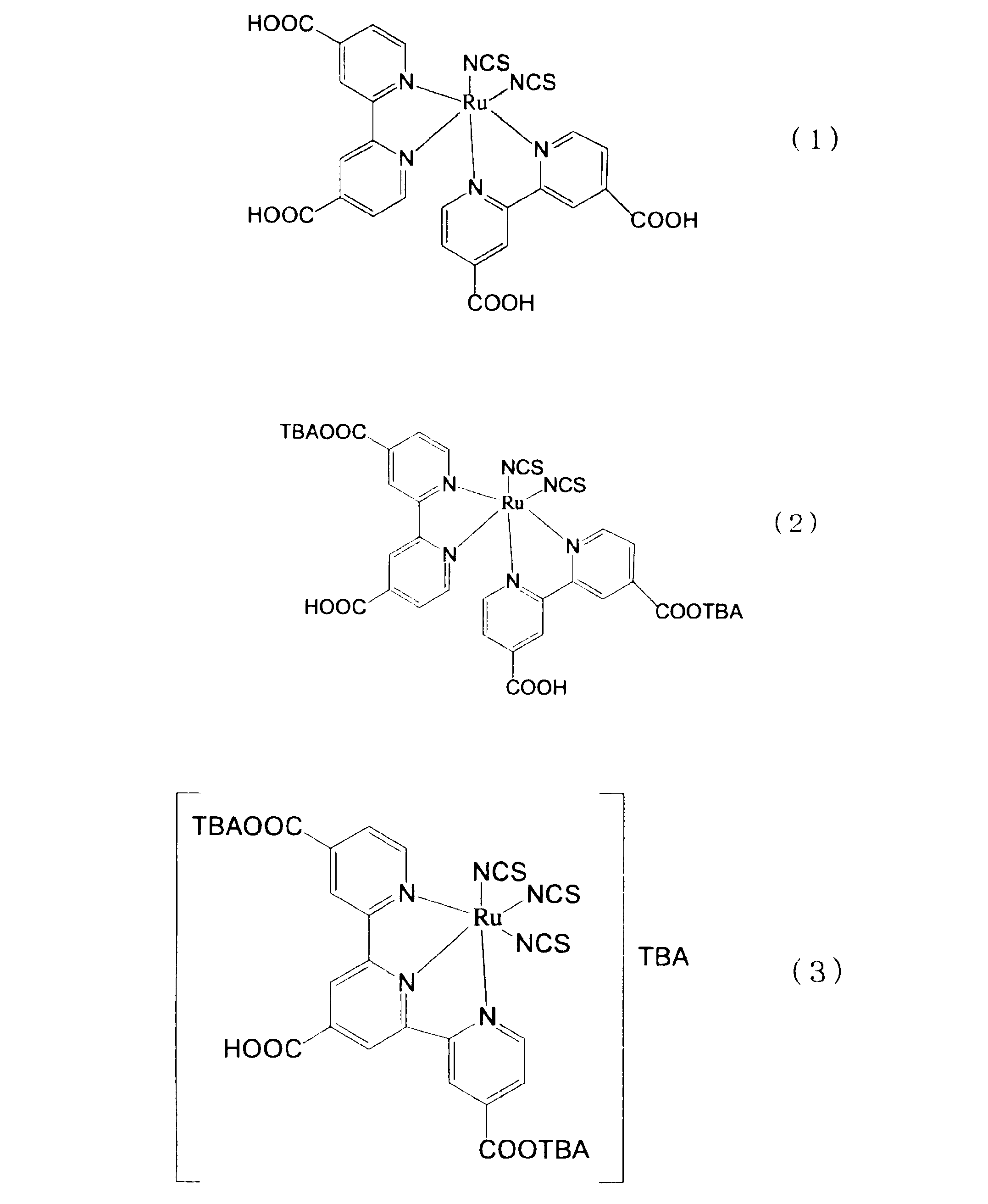
多孔質半導体層6に色素を吸着させる方法としては、例えば、導電性基板A上に触媒層3、多孔性絶縁層4、第二導電層5および多孔性半導体層6が形成された積層体を、色素を溶解した溶液(色素吸着用溶液)に浸漬する方法が代表的なものとして挙げられる。
吸着に際して、色素吸着溶液を多孔性半導体層内の微細孔奥部まで浸透させる上で、色素吸着溶液を加熱してもよい。
電解質7は、酸化還元種を含む液状物であり、一般に電池や太陽電池などに使用される電解質であれば特に限定されない。
酸化還元種としては、I-/I3-系、Br2-/Br3-系、Fe2+/Fe3+系、キノン/ハイドロキノン系などが挙げられる。具体的には、ヨウ化リチウム(LiI)、ヨウ化ナトリウム(NaI)、ヨウ化カリウム(KI)、ヨウ化カルシウム(CaI2)などの金属ヨウ化物とヨウ素(I2)の組み合わせ、テトラエチルアンモニウムアイオダイド(TEAI)、テトラプロピルアンモニウムアイオダイド(TPAI)、テトラブチルアンモニウムアイオダイド(TBAI)、テトラヘキシルアンモニウムアイオダイド(THAI)などのテトラアルキルアンモニウム塩とヨウ素の組み合わせ、および臭化リチウム(LiBr)、臭化ナトリウム(NaBr)、臭化カリウム(KBr)、臭化カルシウム(CaBr2)などの金属臭化物と臭素の組み合わせが好ましく、これらの中でも、LiIとI2の組み合わせが特に好ましい。
このような添加剤としては、t-ブチルピリジン(TBP)などの含窒素芳香族化合物、ジメチルプロピルイミダゾールアイオダイド(DMPII)、メチルプロピルイミダゾールアイオダイド(MPII)、エチルメチルイミダゾールアイオダイド(EMII)、エチルイミダゾールアイオダイド(EII)、ヘキシルメチルイミダゾールアイオダイド(HMII)などのイミダゾール塩が挙げられる。
電解質中の電解質(酸化還元種)濃度は、0.001~1.5モル/リットルの範囲が好ましく、0.01~0.7モル/リットルの範囲が特に好ましい。
カバー部材8としては、受光面側に設ける場合には透光性を有すると共に、封止部と共に電解液の漏洩を防ぐことができるものであればよい。
カバー部材を構成する材料としては、例えば、強化ガラス、強化ガラス以外のガラス板、透明または不透明のプラスチックシート(フィルム、ラミネートフィルム)、セラミックなどが挙げられ、太陽電池を屋外に設置する場合には強化ガラスが特に好ましい。
透明プラスチックシートを用いる場合には、基板1の非受光面側と多孔性半導体層6の受光面側とに2枚のプラスチックシートを配置し、それらの外周縁を熱融着することにより太陽電池全体を封止することができ、後述の封止部を省略することができる。
封止部9は、太陽電池内部の電解液の漏れを防止する機能、基板1や強化ガラスなどの支持体に作用する落下物や応力(衝撃)を吸収する機能および長期にわたる使用時において支持体に作用するたわみなどを吸収する機能を有する。上記のようにカバー部材8として強化ガラスやその他のガラス板を用いた場合には、封止部8を設けることが好ましい。
また、本発明の太陽電池の少なくとも2つ以上を直列に接続して太陽電池モジュールを作製する場合、太陽電池間の電解液の移動を防止するために封止部はセル間絶縁層として機能するため重要である。
紫外線硬化樹脂としては、スリーボンド社製、型番:31X-101、熱硬化性樹脂としては、スリーボンド社製、型番:31X-088や一般に市販されているエポキシ樹脂などを用いることができる。
図2は、本発明の太陽電池(実施形態1-1)を複数個電気的に直列接続してなる太陽電池モジュール(実施形態1-2)の要部の層構成を示す概略断面図である。
この太陽電池モジュールは次のようにして製造することができる。
まず、基板1上に形成された第一導電層を所定間隔でレーザスクライブ法によりパターニングして、導電層が除去されたスクライブラインを複数本形成する。これにより、相互に電気的に分離した複数の第一導電層2が形成され、各第一導電層2上が太陽電池形成領域となる。
なお、複数の第一導電層2のうち、スクライブライン10と直交する方向の一方端側の第一導電層2は幅を小さくして形成され、この幅の小さい第一導電層2上には太陽電池は形成されず、この第一導電層2は隣接する太陽電池の第二電極層5の引出し電極として利用される。
次いで、実施形態1-1と同様にして多孔性半導体層6に増感色素を吸着させる。
次いで、第一導電層2の外周部および第一導電層2における隣接する太陽電池形成領域間に封止材料を塗布し、封止材料上および多孔性半導体層6上に透明カバー部材7(例えば、強化ガラス)を載置し、封止材料を硬化させて封止部(およびセル間絶縁層)9を形成する。
なお、この太陽電池モジュールを構成する各層の形成方法および材料の選択などは、実施形態1-1の太陽電池に準ずる。
図3は、本発明の太陽電池(実施形態2-1)の要部の層構成を示す概略断面図である。
この太陽電池は、実施形態1-1における多孔性絶縁層4上に多孔性半導体層6が形成され、その多孔性半導体層6上に第二導電層5が形成されるタイプであり、多孔性半導体層6が多孔性絶縁層4上から引出し電極にわたって形成されていること、第二導電層5が多孔性半導体層6上から狭い第一導電層2にわたって形成されていること以外は、実施形態1-1と概ね同様である。なお、この太陽電池では、多孔性半導体層6上に第二導電層5が形成されるため、多孔性半導体層6の表面粗さ係数Raが多孔性半導体層と第二導電層との界面の表面粗さ係数Raとなる。
実施形態2-1における太陽電池の製造方法は、基本的に実施形態1-1の製造方法に準ずる。
図4は、本発明の太陽電池(実施形態2-1)を複数個電気的に直列接続してなる太陽電池モジュール(実施形態2-2)の要部の層構成を示す概略断面図である。
この太陽電池モジュールの製造方法は、実施形態1-2の太陽電池モジュールにおける多孔性半導体層6と第二導電層5の作製順が入れ替わること以外は実施形態1-2の製造方法と同様である。
図6は、本発明の太陽電池(実施形態3-1)の要部の層構成を示す概略断面図である。
この太陽電池は、多孔性絶縁層、第二導電層および触媒層がこの順で積層されたタイプであり、具体的には、基板1上に第一導電層2が形成されてなる導電性基板Aと、第一導電層2上に順次形成された、増感色素が吸着されかつ内部に電解質を含有する多孔性半導体層、内部に電解質を含有する多孔性絶縁層、第二導電層および触媒層とを備えている。また、導電性基板Aとカバー部材8との間の外周部に封止部9が設けられている。
また、多孔性絶縁層4は、スクライブライン10をわたって形成され、第二導電層5は、多孔性絶縁層4上から前記幅の狭い第一導電層上にわたって形成されている。第二導電層5と電気的に接続された幅の狭い第一導電層は、第二導電層5の引出し電極となる。
上記のように第二導電層5は、多孔性絶縁層4と強固に接着(接触)しつつ、多孔性絶縁層4および第二導電層5を介した多孔性半導体層3と触媒層3の間のイオンの移動がスムーズに行われるようにする必要がある。そのためには、接触面積を十分確保しつつ、イオンの移動がスムーズに行えるための小孔がある必要がある。このような第二導電層5を形成するためには、その土台となる多孔性絶縁層の膜表面形状が重要となる。
このような本発明の思想は、表面の平坦化を重視する特許文献5に記載の発明とは全く異なる。
したがって、多孔性絶縁層の形成時にその表面粗さ係数Raを制御する必要があり、その制御方法は、実施形態1-1に準ずる。
したがって、第二導電層が緻密な構造をなす場合には、第二導電層が、色素および電解質を流通させる複数の小孔を有するのが好ましく、その形成方法は、実施形態1-1に準ずる。
一方、後述する実施形態4-1のような多孔性絶縁層上に触媒層を形成する場合には、同様に多孔性絶縁層の表面粗さ係数Raを制御することにより、多孔性絶縁層の触媒層における接触面の凹凸形状を制御することができる。
図7は、本発明の太陽電池(実施形態3-1)を複数個電気的に直列接続してなる太陽電池モジュール(実施形態3-2)の要部の層構成を示す概略断面図である。
この太陽電池モジュールは次のようにして製造することができる。
まず、基板1上に形成された第一導電層を所定間隔でレーザスクライブ法によりパターニングして、導電層が除去されたスクライブラインを複数本形成する。これにより、相互に電気的に分離した複数の第一導電層2が形成され、各第一導電層2上が太陽電池形成領域となる。
なお、複数の第一導電層2のうち、スクライブライン10と直交する方向の一方端側の第一導電層2は幅を小さくして形成され、この幅の小さい第一導電層2上には太陽電池は形成されず、この第一導電層2は隣接する太陽電池の第二電極層5の引出し電極として利用される。
次いで、実施形態3-1と同様にして多孔性半導体層6に増感色素を吸着させる。
次いで、第一導電層2の外周部および第一導電層2における隣接する太陽電池形成領域間に封止材料を塗布し、封止材料上および多孔性半導体層6上にカバー部材8を載置し、封止材料を硬化させて封止部(およびセル間絶縁層)9を形成する。
なお、この太陽電池モジュールを構成する各層の形成方法および材料の選択などは、実施形態3-1の太陽電池に準ずる。
図8は、本発明の太陽電池(実施形態4-1)の要部の層構成を示す概略断面図である。
この太陽電池は、実施形態3-1における多孔性絶縁層4上に触媒層および第二導電層がこの順で積層されたタイプであり、第二導電層5が触媒層3の上に形成されていること以外は、実施形態1-1と概ね同様である。なお、この太陽電池では、多孔性絶縁層4上に触媒層3が形成されるため、多孔性絶縁層4の表面粗さ係数Raが多孔性絶縁層の触媒層における接触面の表面粗さ係数Raとなる。
実施形態4-1における太陽電池の製造方法は、基本的に実施形態3-1の製造方法に準ずる。
図4は、本発明の太陽電池(実施形態4-1)を複数個電気的に直列接続してなる太陽電池モジュール(実施形態4-2)の要部の層構成を示す概略断面図である。
この太陽電池モジュールの製造方法は、実施形態3-2の太陽電池モジュールにおける第二導電層5と触媒層3の作製順が入れ替わること以外は実施形態3-2の製造方法と同様である。
実施例および比較例における各層の膜厚および表面粗さ係数Raは、特に断りのない限り、表面粗さ測定機(株式会社東京精密製、型式:サーフコム1400A)を用いて測定した。
図2に示される太陽電池モジュールを作製した。
ガラスからなる基板上1にSnO2膜からなる第一導電層2が成膜された、70mm×70mm×厚さ4mmの導電性ガラス基板(日本板硝子株式会社製、SnO2膜付ガラス)を用意した。
YAGレーザー(西進商事株式会社製、基本波長:1.06μm)を用いて、第一導電層2にレーザー光を照射しSnO2膜を蒸発させて、幅0.1mmのスクライブライン10を6mm間隔で6本形成した。
スクリーン印刷機(ニューロング精密工業株式会社製、型式:LS-34TVA)およびスクリーン版(5mm×50mmの開口部7個)を用いて、導電性ガラス基板上に、触媒形成材料(Solaronix社製、製品名:Pt-Catalyst T/SP)を塗布し、得られた塗膜を450℃で1時間焼成してクラスター状の触媒層3を形成した。
酸化ジルコニウムの微粒子(粒径100nm、シーアイ化成株式会社製)65重量部をテルピネオール30重量部に分散させ、さらにエチルセルロース5重量部を混合してペーストを調製した。
スクリーン印刷機(ニューロング精密工業株式会社製、型式:LS-34TVA)およびスクリーン版(6mm×54mmの開口部7個)を用いて、得られたペーストを触媒層3上に塗布し、25℃で30分間レベリングを行った。
次いで、得られた塗膜を80℃で20分間予備乾燥し、450℃で1時間焼成して、膜厚5μm、表面粗さ係数Ra0.050μmの多孔性絶縁層(酸化ジルコニウム膜)4を形成した。
電子ビーム蒸着器(アルバック株式会社製、型式:ei-5)およびメタルマスク(6.2mm×52mmの開口部7個)を用いて、多孔性絶縁層4上にチタンを蒸着速度5Å/Sで成膜して、膜厚約500nm、表面粗さ係数Ra0.051μmの第二導電層5を形成した。
スクリーン印刷機(ニューロング精密工業株式会社製、型式:LS-34TVA)およびスクリーン版(5mm×50mmの開口部7個)を用いて、市販の酸化チタンペースト(Solaronix社製、製品名:Ti-Nanoxide D/SP、平均粒径13nm)を第二導電層5上に塗布し、25℃で15分間レベリングを行った。
次いで、得られた塗膜を80℃で20分間予備乾燥した後、450℃で1時間焼成し、この工程を5回繰り返して、合計膜厚30μm、最外層の表面粗さ係数Ra0.051μmの多孔性半導体層(酸化チタン膜)6を形成した。
増感色素(Solaronix社製、製品名:Ruthenium620-1H3TBA)を、濃度4×10⁻⁴モル/リットルになるように、体積比1:1のアセトニトリル(Aldrich Chemical Company製)とt-ブチルアルコール(Aldrich Chemical Company製)の混合溶剤に溶解させて色素吸着用溶液を得た。
前記工程を経て得られた積層体を色素吸着用溶液に40℃の温度条件で20時間浸漬し、増感色素を多孔質半導体層6に吸着させた。その後、積層体をエタノール(Aldrich Chemical Company製)で洗浄し、約80℃で約10分間乾燥させた。
溶剤としてのアセトニトリルに、酸化還元種としてLiI(Aldrich Chemical Company製)が濃度0.1モル/リットル、I2(東京化成工業株式会社製)が濃度0.01モル/リットルとなるように、さらに添加剤としてt-ブチルピリジン(TBP、Aldrich Chemical Company製)が濃度0.5モル/リットル、ジメチルプロピルイミダゾールアイオダイド(DMPII、四国化成工業株式会社製)が濃度0.6モル/リットルとなるように添加し、溶解させて電解質を調製した。
第一導電層2上における周囲部と太陽電池形成領域間に、紫外線硬化材(スリーボンド社製、型番:31X-101)を塗布し、別途用意した50mm×70mm×厚さ4.0mmの強化ガラス基板8(旭硝子株式会社製)と基板1とを貼り合せた。基板1には予め電解質注入用孔を設けておいた。次いで、紫外線照射ランプ(EFD社製、型式:Novacure)を用いて塗布部分に紫外線を照射して紫外線硬化材を硬化させて封止部9を形成すると共に、2枚の基板1、8を固定した。
次いで、基板1の電解質注入用孔から電解質を注入し、電解質注入用孔を樹脂にて封止することにより、図2に相当する太陽電池モジュールを完成した。
また、同様にして太陽電池モジュールを10個作製し、作製時に多孔性半導体層と第二導電層の剥離の有無を目視で観察した。
得られた結果を、第二導電層および多孔性絶縁層の表面粗さ係数Raと共に表1に示す。
多孔性絶縁層4の形成において、多孔性絶縁層用ペースト塗布後のレベリング時間を0秒、20秒、2分および5分に変化させたこと以外は、実施例1-1と同様にして図2に示される太陽電池モジュールを作製し、その各種太陽電池特性を測定した。
多孔性絶縁層の表面粗さ係数Raは、それぞれ0.190μm、0.147μm、0.099μm、0.055μmに変化し、それに伴い第二導電層の表面粗さ係数Raは、0.198μm、0.150μm、0.101μm、0.053μmに変化した。
また、同様にして太陽電池モジュールを10個作製し、作製時に多孔性半導体層と第二導電層の剥離の有無を目視で観察した。
得られた結果を、第二導電層および多孔性絶縁層の表面粗さ係数Raと共に表1に示す。
多孔性絶縁層4の形成において、多孔性絶縁層用ペースト塗布後に、35℃で10分間レベリングを行ったこと以外は、実施例1-1と同様にして図2に示される太陽電池モジュールを作製し、その各種太陽電池特性を測定した。
多孔性絶縁層の表面粗さ係数Raは0.043μmに変化し、それに伴い第二導電層の表面粗さ係数は0.043μmに変化した。
また、同様にして太陽電池モジュールを10個作製し、作製時に多孔性半導体層と第二導電層の剥離の有無を目視で観察した。
得られた結果を、第二導電層および多孔性絶縁層の表面粗さ係数Raと共に表1に示す。
多孔性絶縁層4の形成において、酸化ジルコニウムの微粒子(粒径100nm、シーアイ化成株式会社製)60重量部をテルピネオール35重量部に分散させ、さらにエチルセルロース5重量部を混合してペーストを調製したこと、および多孔性絶縁層用ペースト塗布後のレベリング時間を10分に変化させたこと以外は、実施例1-1と同様にして図2に示される太陽電池モジュールを作製し、その各種太陽電池特性を測定した。
多孔性絶縁層の表面粗さ係数Raは0.036μmに変化し、それに伴い第二導電層の表面粗さ係数は0.033μmに変化した。
また、同様にして太陽電池モジュールを10個作製し、作製時に多孔性半導体層と第二導電層の剥離の有無を目視で観察した。
得られた結果を、第二導電層および多孔性絶縁層の表面粗さ係数Raと共に表1に示す。
多孔性絶縁層4の形成において、酸化ジルコニウムの微粒子(粒径100nm、シーアイ化成株式会社製)60重量部をテルピネオール35重量部に分散させ、さらにエチルセルロース5重量部を混合してペーストを調製したこと(比較例1-2と同様)、および多孔性絶縁層用ペースト塗布後に、35℃で10分間レベリングを行ったこと(比較例1-1と同様)以外は、実施例1-1と同様にして図2に示される太陽電池モジュールを作製し、その各種太陽電池特性を測定した。
多孔性絶縁層の表面粗さ係数Raは0.026μmに変化し、それに伴い第二導電層の表面粗さ係数は0.020μmに変化した。
また、同様にして太陽電池モジュールを10個作製し、作製時に多孔性半導体層と第二導電層の剥離の有無を目視で観察した。
得られた結果を、第二導電層および多孔性絶縁層の表面粗さ係数Raと共に表1に示す。
強化ガラス基板8の代わりに同サイズの導電性ガラス基板(日本板硝子株式会社製、SnO2膜付ガラス)を用いたこと(特許文献5と同様)、および多孔性絶縁層4の形成において、多孔性絶縁層用ペースト塗布後に、35℃で10分間レベリングを行ったこと(比較例1-1と同様)以外は、実施例1-1と同様にして図2に示される太陽電池モジュールを作製し、その各種太陽電池特性を測定した。
多孔性絶縁層の表面粗さ係数Raは0.043μmに変化し、それに伴い第二導電層の表面粗さ係数は0.043μmに変化した。
また、同様にして太陽電池モジュールを10個作製し、作製時に多孔性半導体層と第二導電層の剥離の有無を目視で観察した。
得られた結果を、第二導電層および多孔性絶縁層の表面粗さ係数Raと共に表1に示す。

第二導電層5と多孔性半導体層6との形成順を入れ替えたこと以外は、実施例1-1と同様にして、図4に示される太陽電池モジュールを作製し、その各種太陽電池特性を測定した。
多孔性半導体層の表面粗さ係数Raは0.051μmであった。
また、同様にして太陽電池モジュールを10個作製し、作製時に多孔性半導体層と第二導電層の剥離の有無を目視で観察した。
得られた結果を、多孔性半導体層の表面粗さ係数Raと共に表2に示す。
多孔性半導体層6の形成において、多孔性半導体層用ペースト塗布後のレベリング時間を0秒、30秒、2分、5分に変化させたこと以外は、実施例1-6と同様にして図4に示される太陽電池モジュールを作製し、その各種太陽電池特性を測定した。
多孔性半導体層の表面粗さ係数Raは、それぞれ0.240μm、0.170μm、0.104μm、0.086μmに変化した。
また、同様にして太陽電池モジュールを10個作製し、作製時に多孔性半導体層と第二導電層の剥離の有無を目視で観察した。
得られた結果を、多孔性半導体層の表面粗さ係数Raと共に表2に示す。
多孔性半導体層6の形成において、多孔性半導体層用ペースト塗布後に、30℃で10分間レベリングを行ったこと以外は、実施例1-6と同様にして図4に示される太陽電池モジュールを作製し、その各種太陽電池特性を測定した。
多孔性半導体層の表面粗さ係数Raは0.040μmであった。
また、同様にして太陽電池モジュールを10個作製し、作製時に多孔性半導体層と第二導電層の剥離の有無を目視で観察した。
得られた結果を、多孔性半導体層の表面粗さ係数Raと共に表2に示す。
多孔性半導体層6の形成において、多孔性半導体層用ペースト塗布後に、35℃で10分間レベリングを行ったこと以外は、実施例1-6と同様にして図4に示される太陽電池モジュールを作製し、その各種太陽電池特性を測定した。
多孔性半導体層の表面粗さ係数Raは0.030μmであった。
また、同様にして太陽電池モジュールを10個作製し、作製時に多孔性半導体層と第二導電層の剥離の有無を目視で観察した。
得られた結果を、多孔性半導体層の表面粗さ係数Raと共に表2に示す。
多孔性半導体層6の形成において、多孔性半導体層用ペースト塗布後に、40℃で10分間レベリングを行ったこと以外は、実施例1-6と同様にして図4に示される太陽電池モジュールを作製し、その各種太陽電池特性を測定した。
多孔性半導体層の表面粗さ係数Raは0.031μmであった。
また、同様にして太陽電池モジュールを10個作製し、作製時に多孔性半導体層と第二導電層の剥離の有無を目視で観察した。
得られた結果を、多孔性半導体層の表面粗さ係数Raと共に表2に示す。

図中、「○」は前者の結果、第二導電層の表面粗さ係数とFFとの点、「□」は後者の結果、多孔性半導体層の表面粗さ係数とFFとの点を示す。
図5によれば、表面粗さ係数0.05μm付近にFFの変曲点があり、このことは、多孔性半導体層の第二導電層における接触面の表面粗さ係数が大きくなれば、電子移動界面の接触面積が大きくなり抵抗が小さくなることを示している。
図7に示される太陽電池モジュールを作製した。
ガラスからなる基板上1にSnO2膜からなる第一導電層2が成膜された、70mm×70mm×厚さ4mmの導電性ガラス基板(日本板硝子株式会社製、SnO2膜付ガラス)を用意した。
YAGレーザー(西進商事株式会社製、基本波長:1.06μm)を用いて、第一導電層2にレーザー光を照射しSnO2膜を蒸発させて、幅0.1mmのスクライブライン10を6mm間隔で6本形成した。
スクリーン印刷機(ニューロング精密工業株式会社製、型式:LS-34TVA)およびスクリーン版(5mm×50mmの開口部7個)を用いて、市販の酸化チタンペースト(Solaronix社製、製品名:Ti-Nanoxide D/SP、平均粒径13nm)を第一導電層2上に塗布し、25℃で15分間レベリングを行った。
次いで、得られた塗膜を80℃で20分間予備乾燥した後、450℃で1時間焼成し、この工程を5回繰り返して、合計膜厚30μm、最外層の表面粗さ係数Ra0.051μmの多孔性半導体層(酸化チタン膜)6を形成した。
酸化ジルコニウムの微粒子(粒径100nm、シーアイ化成株式会社製)65重量部をテルピネオール30重量部に分散させ、さらにエチルセルロース5重量部を混合してペーストを調製した。
スクリーン印刷機(ニューロング精密工業株式会社製、型式:LS-34TVA)およびスクリーン版(6mm×54mmの開口部7個)を用いて、得られたペーストを多孔性半導体層6上に塗布し、25℃で30分間レベリングを行った。
次いで、得られた塗膜を80℃で20分間予備乾燥し、450℃で1時間焼成して、膜厚5μm、表面粗さ係数Ra0.050μmの多孔性絶縁層(酸化ジルコニウム膜)4を形成した。
電子ビーム蒸着器(アルバック株式会社製、型式:ei-5)およびメタルマスク(5.8mm×52mmの開口部7個)を用いて、多孔性絶縁層4上にチタンを蒸着速度5Å/Sで成膜して、膜厚約500nmの第二導電層5を形成した。
スクリーン印刷機(ニューロング精密工業株式会社製、型式:LS-34TVA)およびスクリーン版(5mm×50mmの開口部7個)を用いて、第二導電層5上に、触媒形成材料(Solaronix社製、製品名:Pt-Catalyst T/SP)を塗布し、得られた塗膜を450℃で1時間焼成して触媒層3を形成した。
増感色素(Solaronix社製、製品名:Ruthenium620-1H3TBA)を、濃度4×10⁻⁴モル/リットルになるように、体積比1:1のアセトニトリル(Aldrich Chemical Company製)とt-ブチルアルコール(Aldrich Chemical Company製)の混合溶剤に溶解させて色素吸着用溶液を得た。
前記工程を経て得られた積層体を色素吸着用溶液に40℃の温度条件で20時間浸漬し、増感色素を多孔質半導体層6に吸着させた。その後、積層体をエタノール(Aldrich Chemical Company製)で洗浄し、約80℃で約10分間乾燥させた。
溶剤としてのアセトニトリルに、酸化還元種としてLiI(Aldrich Chemical Company製)が濃度0.1モル/リットル、I2(東京化成工業株式会社製)が濃度0.01モル/リットルとなるように、さらに添加剤としてt-ブチルピリジン(TBP、Aldrich Chemical Company製)が濃度0.5モル/リットル、ジメチルプロピルイミダゾールアイオダイド(DMPII、四国化成工業株式会社製)が濃度0.6モル/リットルとなるように添加し、溶解させて電解質を調製した。
第一導電層2上における周囲部と太陽電池形成領域間に、紫外線硬化材(スリーボンド社製、型番:31X-101)を塗布し、別途用意した50mm×70mm×厚さ1mmのソーダ石灰ガラスからなるカバー部材8と基板1とを貼り合せた。カバー部材8には予め電解質注入用孔を設けておいた。次いで、紫外線照射ランプ(EFD社製、型式:Novacure)を用いて塗布部分に紫外線を照射して紫外線硬化材を硬化させて封止部9を形成すると共に、2枚の基板1、8を固定した。
次いで、カバー部材8の電解質注入用孔から電解質を注入し、電解質注入用孔を樹脂にて封止することにより、図7に相当する太陽電池モジュールを完成した。
また、同様にして太陽電池モジュールを10個作製し、作製時に第二導電層および触媒層の剥離の有無を目視で観察した。
得られた結果を、多孔性絶縁層の表面粗さ係数Raと共に表3に示す。
多孔性絶縁層4の形成において、多孔性絶縁層用ペースト塗布後のレベリング時間を0秒、20秒、2分および5分に変化させたこと以外は、実施例2-1と同様にして図7に示される太陽電池モジュールを作製し、その各種太陽電池特性を測定した。
多孔性絶縁層の表面粗さ係数Raは、それぞれ0.190μm、0.147μm、0.099μm、0.055μmに変化した。
また、同様にして太陽電池モジュールを10個作製し、作製時に第二導電層および触媒層の剥離の有無を目視で観察した。
得られた結果を、多孔性絶縁層の表面粗さ係数Raと共に表3に示す。
多孔性絶縁層4の形成において、酸化ジルコニウムの微粒子65重量部をテルピネオール28重量部に分散させ、さらにエチルセルロース7重量部を混合したペーストを用いたこと、およびスクリーン印刷後に30℃で3分間レベリングを行ったこと以外は実施例2-1と同様にして図7の構造の太陽電池モジュールを作製し、その各種太陽電池特性を測定した。
多孔性絶縁層の表面粗さ係数Raは0.300μmに変化した。
また、同様にして太陽電池モジュールを10個作製し、作製時に第二導電層および触媒層の剥離の有無を目視で観察した。
得られた結果を、多孔性絶縁層の表面粗さ係数Raと共に表3に示す。
多孔性絶縁層4の形成において、多孔性絶縁層用ペースト塗布後に、30℃で10分間レベリングを行ったこと以外は、実施例2-1と同様にして図7に示される太陽電池モジュールを作製し、その各種太陽電池特性を測定した。
多孔性絶縁層の表面粗さ係数Raは0.043μmに変化した。
また、同様にして太陽電池モジュールを10個作製し、作製時に第二導電層および触媒層の剥離の有無を目視で観察した。
得られた結果を、多孔性絶縁層の表面粗さ係数Raと共に表3に示す。
多孔性絶縁層4の形成において、多孔性絶縁層用ペースト塗布後に、35℃で10分間レベリングを行ったこと以外は、実施例2-1と同様にして図7に示される太陽電池モジュールを作製し、その各種太陽電池特性を測定した。
多孔性絶縁層の表面粗さ係数Raは0.036μmに変化した。
また、同様にして太陽電池モジュールを10個作製し、作製時に第二導電層および触媒層の剥離の有無を目視で観察した。
得られた結果を、多孔性絶縁層の表面粗さ係数Raと共に表3に示す。
多孔性絶縁層4の形成において、多孔性絶縁層用ペースト塗布後に、25℃で10分間レベリングを行ったこと以外は、実施例2-1と同様にして図7に示される太陽電池モジュールを作製し、その各種太陽電池特性を測定した。
多孔性絶縁層の表面粗さ係数Raは0.320μmに変化した。
また、同様にして太陽電池モジュールを10個作製し、作製時に第二導電層および触媒層の剥離の有無を目視で観察した。
得られた結果を、多孔性絶縁層の表面粗さ係数Raと共に表3に示す。
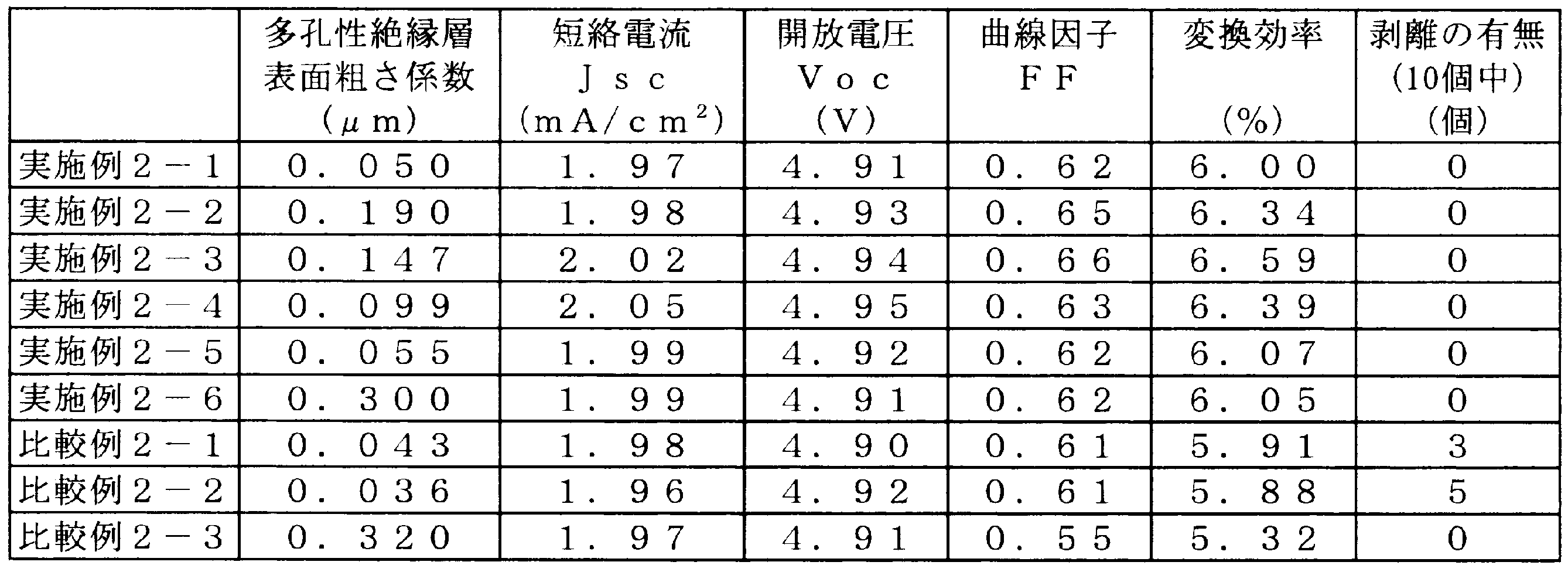
第二導電層5と触媒層3との形成順を入れ替えたこと以外は、実施例2-1と同様にして、図9に示される太陽電池モジュールを作製し、その各種太陽電池特性を測定した。
多孔性半導体層の表面粗さ係数Raは0.050μmであった。
また、同様にして太陽電池モジュールを10個作製し、作製時に第二導電層および触媒層の剥離の有無を目視で観察した。
得られた結果を、多孔性絶縁層の表面粗さ係数Raと共に表4に示す。
多孔性絶縁層4の形成において、多孔性半導体層用ペースト塗布後のレベリング時間を0秒、20秒、2分および5分に変化させたこと以外は、実施例2-7と同様にして図9に示される太陽電池モジュールを作製し、その各種太陽電池特性を測定した。
多孔性半導体層の表面粗さ係数Raは、それぞれ0.190μm、0.147μm、0.099μm、0.055μmに変化した。
また、同様にして太陽電池モジュールを10個作製し、作製時に第二導電層および触媒層の剥離の有無を目視で観察した。
得られた結果を、多孔性絶縁層の表面粗さ係数Raと共に表4に示す。
多孔性絶縁層4の形成において、酸化ジルコニウムの微粒子65重量部をテルピネオール28重量部に分散させ、さらにエチルセルロース7重量部を混合したペーストを用いたこと、およびスクリーン印刷後に30℃で3分間レベリングを行ったこと以外は実施例2-7と同様にして図9の構造の太陽電池モジュールを作製し、その各種太陽電池特性を測定した。
多孔性絶縁層の表面粗さ係数Raは0.300μmに変化した。
また、同様にして太陽電池モジュールを10個作製し、作製時に第二導電層および触媒層の剥離の有無を目視で観察した。
得られた結果を、多孔性絶縁層の表面粗さ係数Raと共に表4に示す。
多孔性絶縁層4の形成において、多孔性絶縁層用ペースト塗布後に、30℃で10分間レベリングを行ったこと以外は、実施例2-7と同様にして図9に示される太陽電池モジュールを作製し、その各種太陽電池特性を測定した。
多孔性絶縁層の表面粗さ係数Raは0.043μmに変化した。
また、同様にして太陽電池モジュールを10個作製し、作製時に第二導電層および触媒層の剥離の有無を目視で観察した。
得られた結果を、多孔性絶縁層の表面粗さ係数Raと共に表4に示す。
多孔性絶縁層4の形成において、多孔性絶縁層用ペースト塗布後に、35℃で10分間レベリングを行ったこと以外は、実施例2-7と同様にして図9に示される太陽電池モジュールを作製し、その各種太陽電池特性を測定した。
多孔性絶縁層の表面粗さ係数Raは0.036μmに変化した。
また、同様にして太陽電池モジュールを10個作製し、作製時に第二導電層および触媒層の剥離の有無を目視で観察した。
得られた結果を、多孔性絶縁層の表面粗さ係数Raと共に表4に示す。
多孔性絶縁層4の形成において、多孔性絶縁層用ペースト塗布後に、25℃で10分間レベリングを行ったこと以外は、実施例2-7と同様にして図9に示される太陽電池モジュールを作製し、その各種太陽電池特性を測定した。
多孔性絶縁層の表面粗さ係数Raは0.320μmに変化した。
また、同様にして太陽電池モジュールを10個作製し、作製時に第二導電層および触媒層の剥離の有無を目視で観察した。
得られた結果を、多孔性絶縁層の表面粗さ係数Raと共に表4に示す。

2 第一導電層
3 触媒層
4 多孔性絶縁層
5 第二導電層
6 多孔性半導体層
7 電解質
8 カバー部材(透光性カバー部材、強化ガラス)
9 封止部(セル間絶縁層)
10 スクライブライン
A 導電性基板
Claims (13)
- 第一導電層上に、少なくとも触媒層、内部に電解質を含有する多孔性絶縁層、増感色素が吸着されかつ内部に電解質を含有する多孔性半導体層および第二導電層が積層され、隣接して積層された、前記多孔性絶縁層または多孔性半導体層の前記触媒層または前記第二導電層における接触面が表面粗さ係数Ra0.05~0.3μmの範囲内の凹凸形状を有している色素増感太陽電池。
- 前記色素増感太陽電池が、
第一導電層上に、少なくとも触媒層、内部に電解質を含有する多孔性絶縁層、増感色素が吸着されかつ内部に電解質を含有する多孔性半導体層がこの順で積層され、前記多孔性絶縁層と前記多孔性半導体層の間に第二導電層が積層されてなる構造、
第一導電層上に、少なくとも触媒層、内部に電解質を含有する多孔性絶縁層、増感色素が吸着されかつ内部に電解質を含有する多孔性半導体層がこの順で積層され、さらに多孔性半導体層上に第二導電層が積層されてなる構造、
第一導電層上に、少なくとも増感色素が吸着されかつ内部に電解質を含有する多孔性半導体層、内部に電解質を含有する多孔性絶縁層、第二導電層および触媒層が積層され、前記多孔性絶縁層、前記第二導電層および前記触媒層がこの順で積層されてなる構造、または
第一導電層上に、少なくとも増感色素が吸着されかつ内部に電解質を含有する多孔性半導体層、内部に電解質を含有する多孔性絶縁層、第二導電層および触媒層が積層され、前記多孔性絶縁層、前記触媒層および前記第二導電層がこの順で積層されてなる構造
を有している請求項1に記載の色素増感太陽電池。 - 第一導電層上に、少なくとも触媒層、内部に電解質を含有する多孔性絶縁層、増感色素が吸着されかつ内部に電解質を含有する多孔性半導体層および第二導電層が積層され、前記多孔性半導体層と前記第二導電層とが隣接して積層されかつ前記多孔性半導体層の前記第二導電層における接触面が表面粗さ係数Ra0.05~0.3μmの範囲内の凹凸形状を有している請求項1に記載の色素増感太陽電池。
- 第一導電層上に、少なくとも触媒層、内部に電解質を含有する多孔性絶縁層、増感色素が吸着されかつ内部に電解質を含有する多孔性半導体層がこの順で積層され、前記多孔性絶縁層と前記多孔性半導体層の間に第二導電層が積層されてなる請求項3に記載の色素増感太陽電池。
- 第一導電層上に、少なくとも触媒層、内部に電解質を含有する多孔性絶縁層、増感色素が吸着されかつ内部に電解質を含有する多孔性半導体層がこの順で積層され、さらに多孔性半導体層上に第二導電層が積層されてなる請求項3に記載の色素増感太陽電池。
- 第一導電層上に、少なくとも増感色素が吸着されかつ内部に電解質を含有する多孔性半導体層、内部に電解質を含有する多孔性絶縁層、第二導電層および触媒層が積層され、前記多孔性絶縁層と前記第二導電層または前記触媒層とが隣接して積層されかつ前記多孔性絶縁層の前記第二導電層または前記触媒層における接触面が表面粗さ係数Ra0.05~0.3μmの範囲内の凹凸形状を有している請求項1に記載の色素増感太陽電池。
- 第一導電層上に、少なくとも増感色素が吸着されかつ内部に電解質を含有する多孔性半導体層、内部に電解質を含有する多孔性絶縁層、第二導電層および触媒層が積層され、前記多孔性絶縁層、前記第二導電層および前記触媒層がこの順で積層されてなる請求項6に記載の色素増感太陽電池。
- 第一導電層上に、少なくとも増感色素が吸着されかつ内部に電解質を含有する多孔性半導体層、内部に電解質を含有する多孔性絶縁層、第二導電層および触媒層が積層され、前記多孔性絶縁層、前記触媒層および前記第二導電層がこの順で積層されてなる請求項6に記載の色素増感太陽電池。
- 前記第一導電層および第二導電層が、金属材料または金属酸化物材料からなる請求項1に記載の色素増感太陽電池。
- 前記金属材料が、チタン、ニッケルまたはタンタルである請求項9に記載の色素増感太陽電池。
- 前記金属酸化物材料が、酸化錫、フッ素がドープされた酸化錫、酸化亜鉛、酸化インジウムまたはインジウム錫複合酸化物である請求項9に記載の色素増感太陽電池。
- 前記第二導電層が、前記電解質、または前記色素および電解質を流通させる複数の小孔を有する請求項1に記載の色素増感太陽電池。
- 請求項1に記載の色素増感太陽電池の2つ以上が電気的に直列接続されてなる色素増感太陽電池モジュール。
Priority Applications (5)
| Application Number | Priority Date | Filing Date | Title |
|---|---|---|---|
| ES10764360.3T ES2467924T3 (es) | 2009-04-15 | 2010-03-31 | Célula solar sensibilizada por colorante y módulo de células solares sensibilizadas por colorante |
| EP10764360.3A EP2421084B1 (en) | 2009-04-15 | 2010-03-31 | Dye-sensitized solar cell and dye-sensitized solar cell module |
| JP2011509257A JP5422645B2 (ja) | 2009-04-15 | 2010-03-31 | 色素増感太陽電池および色素増感太陽電池モジュール |
| US13/263,433 US20120042930A1 (en) | 2009-04-15 | 2010-03-31 | Dye-sensitized solar cell and dye-sensitized solar cell module |
| CN201080016690.XA CN102396101B (zh) | 2009-04-15 | 2010-03-31 | 染料敏化太阳能电池和染料敏化太阳能电池模块 |
Applications Claiming Priority (4)
| Application Number | Priority Date | Filing Date | Title |
|---|---|---|---|
| JP2009-099239 | 2009-04-15 | ||
| JP2009-099238 | 2009-04-15 | ||
| JP2009099239 | 2009-04-15 | ||
| JP2009099238 | 2009-04-15 |
Publications (1)
| Publication Number | Publication Date |
|---|---|
| WO2010119775A1 true WO2010119775A1 (ja) | 2010-10-21 |
Family
ID=42982437
Family Applications (1)
| Application Number | Title | Priority Date | Filing Date |
|---|---|---|---|
| PCT/JP2010/055894 WO2010119775A1 (ja) | 2009-04-15 | 2010-03-31 | 色素増感太陽電池および色素増感太陽電池モジュール |
Country Status (6)
| Country | Link |
|---|---|
| US (1) | US20120042930A1 (ja) |
| EP (1) | EP2421084B1 (ja) |
| JP (1) | JP5422645B2 (ja) |
| CN (1) | CN102396101B (ja) |
| ES (1) | ES2467924T3 (ja) |
| WO (1) | WO2010119775A1 (ja) |
Cited By (12)
| Publication number | Priority date | Publication date | Assignee | Title |
|---|---|---|---|---|
| JP2011028918A (ja) * | 2009-07-22 | 2011-02-10 | Shimane Prefecture | 色素増感太陽電池 |
| US20120211048A1 (en) * | 2009-11-02 | 2012-08-23 | Norio Murofushi | Wet solar cell and wet solar cell module |
| JP2012174383A (ja) * | 2011-02-18 | 2012-09-10 | Sony Corp | 光電変換装置及びその製造方法 |
| JP2012212539A (ja) * | 2011-03-31 | 2012-11-01 | Hitachi Zosen Corp | 色素増感太陽電池における対向電極の製造方法および色素増感太陽電池 |
| WO2014030686A1 (ja) * | 2012-08-22 | 2014-02-27 | 住友大阪セメント株式会社 | 色素増感型太陽電池用ペースト、多孔質光反射絶縁層、及び色素増感型太陽電池 |
| CN103620791A (zh) * | 2011-06-08 | 2014-03-05 | 夏普株式会社 | 光电转换元件以及光电转换元件模块 |
| JP2014116210A (ja) * | 2012-12-10 | 2014-06-26 | International Frontier Technology Laboratory Inc | 2酸化ケイ素ソーラーセル |
| JP2014130766A (ja) * | 2012-12-28 | 2014-07-10 | International Frontier Technology Laboratory Inc | 色素増感タンデム2酸化ケイ素ソーラーセル |
| JP2014203539A (ja) * | 2013-04-01 | 2014-10-27 | ローム株式会社 | 色素増感太陽電池およびその製造方法、および電子機器 |
| JP2015144235A (ja) * | 2013-12-27 | 2015-08-06 | シャープ株式会社 | 光電変換装置作製キット、光電変換装置および光電変換装置付き携帯機器用カバー |
| JP2015211123A (ja) * | 2014-04-25 | 2015-11-24 | シャープ株式会社 | 光電変換素子 |
| US10916382B2 (en) | 2011-06-08 | 2021-02-09 | Sharp Kabushiki Kaisha | Photoelectric conversion element and photoelectric conversion element module |
Families Citing this family (7)
| Publication number | Priority date | Publication date | Assignee | Title |
|---|---|---|---|---|
| SE537669C2 (sv) * | 2012-04-04 | 2015-09-29 | Exeger Sweden Ab | Färgämnessensiterad solcellsmodul med seriekopplad struktursamt sätt för framställning av solcellen |
| CN104380408B (zh) * | 2012-09-01 | 2017-02-22 | 株式会社藤仓 | 色素增感太阳电池元件 |
| CN103441217B (zh) * | 2013-07-16 | 2015-11-04 | 华中科技大学 | 基于钙钛矿类吸光材料的介观太阳能电池及其制备方法 |
| DE102013216848A1 (de) * | 2013-08-23 | 2015-02-26 | Fraunhofer-Gesellschaft zur Förderung der angewandten Forschung e.V. | Langzeitstabile, aus Lösungen abscheidbare photovoltaische Elemente und in-situ-Verfahren zu deren Herstellung |
| SE537836C2 (sv) * | 2014-02-06 | 2015-11-03 | Exeger Sweden Ab | En transparent färgämnessensibiliserad solcell samt ett sättför framställning av densamma |
| JP6773944B2 (ja) * | 2016-01-06 | 2020-10-21 | inQs株式会社 | 光発電素子 |
| CN106090804A (zh) * | 2016-07-27 | 2016-11-09 | 杨炳 | 一种具备自发电功能的户外照明装置 |
Citations (10)
| Publication number | Priority date | Publication date | Assignee | Title |
|---|---|---|---|---|
| JP2664194B2 (ja) | 1988-02-12 | 1997-10-15 | エコル ポリテクニク フェデラル ドゥ ローザンヌ | 光電気化学電池・その製法及び使用法 |
| JPH11514787A (ja) | 1995-10-31 | 1999-12-14 | エコール ポリテクニーク フェデラル ドゥ ローザンヌ | 光起電力セル電池及びその製造方法 |
| JP2001357897A (ja) | 2000-06-14 | 2001-12-26 | Fuji Xerox Co Ltd | 光電変換モジュール |
| JP2002367686A (ja) | 2001-06-12 | 2002-12-20 | Aisin Seiki Co Ltd | 色素増感型太陽電池及びその製造方法 |
| JP2003092417A (ja) | 2001-09-18 | 2003-03-28 | Seiko Epson Corp | 光電変換素子 |
| JP2006147261A (ja) * | 2004-11-17 | 2006-06-08 | Enplas Corp | 色素増感太陽電池の対向電極及び色素増感太陽電池 |
| JP2007134328A (ja) * | 2005-11-11 | 2007-05-31 | Samsung Sdi Co Ltd | 太陽電池及びその製造方法 |
| JP2008146922A (ja) * | 2006-12-07 | 2008-06-26 | Sharp Corp | 光電変換素子および色素増感太陽電池 |
| JP2008153180A (ja) * | 2006-12-20 | 2008-07-03 | Fujikura Ltd | 光電変換素子および光電変換素子用の対極の製造方法 |
| JP2009016304A (ja) * | 2007-07-09 | 2009-01-22 | Sumitomo Osaka Cement Co Ltd | 色素増感型太陽電池用バインダー、ペースト、色素増感型太陽電池用白色性絶縁膜、及び色素増感型太陽電池 |
Family Cites Families (6)
| Publication number | Priority date | Publication date | Assignee | Title |
|---|---|---|---|---|
| JP4087445B2 (ja) | 1995-10-31 | 2008-05-21 | エコール ポリテクニーク フェデラル ドゥ ローザンヌ | 光起電力セル電池及びその製造方法 |
| US6677516B2 (en) * | 2001-01-29 | 2004-01-13 | Sharp Kabushiki Kaisha | Photovoltaic cell and process for producing the same |
| KR100589322B1 (ko) * | 2004-02-03 | 2006-06-14 | 삼성에스디아이 주식회사 | 고효율 염료감응 태양전지 및 그 제조 방법 |
| US20090133741A1 (en) * | 2005-09-02 | 2009-05-28 | Kyocera Corporation | Photoelectric Conversion Device and Method of Manufacturing the Same, and Photoelectric Power Generation Device |
| WO2007043533A1 (ja) * | 2005-10-11 | 2007-04-19 | Kyocera Corporation | 光電変換装置及びその製造方法並びに光発電装置 |
| EP2043190B1 (en) * | 2006-07-06 | 2021-01-06 | Sharp Kabushiki Kaisha | Dye-sensitized solar cell module and method for fabricating same |
-
2010
- 2010-03-31 EP EP10764360.3A patent/EP2421084B1/en not_active Not-in-force
- 2010-03-31 CN CN201080016690.XA patent/CN102396101B/zh active Active
- 2010-03-31 ES ES10764360.3T patent/ES2467924T3/es active Active
- 2010-03-31 US US13/263,433 patent/US20120042930A1/en not_active Abandoned
- 2010-03-31 WO PCT/JP2010/055894 patent/WO2010119775A1/ja active Application Filing
- 2010-03-31 JP JP2011509257A patent/JP5422645B2/ja not_active Expired - Fee Related
Patent Citations (10)
| Publication number | Priority date | Publication date | Assignee | Title |
|---|---|---|---|---|
| JP2664194B2 (ja) | 1988-02-12 | 1997-10-15 | エコル ポリテクニク フェデラル ドゥ ローザンヌ | 光電気化学電池・その製法及び使用法 |
| JPH11514787A (ja) | 1995-10-31 | 1999-12-14 | エコール ポリテクニーク フェデラル ドゥ ローザンヌ | 光起電力セル電池及びその製造方法 |
| JP2001357897A (ja) | 2000-06-14 | 2001-12-26 | Fuji Xerox Co Ltd | 光電変換モジュール |
| JP2002367686A (ja) | 2001-06-12 | 2002-12-20 | Aisin Seiki Co Ltd | 色素増感型太陽電池及びその製造方法 |
| JP2003092417A (ja) | 2001-09-18 | 2003-03-28 | Seiko Epson Corp | 光電変換素子 |
| JP2006147261A (ja) * | 2004-11-17 | 2006-06-08 | Enplas Corp | 色素増感太陽電池の対向電極及び色素増感太陽電池 |
| JP2007134328A (ja) * | 2005-11-11 | 2007-05-31 | Samsung Sdi Co Ltd | 太陽電池及びその製造方法 |
| JP2008146922A (ja) * | 2006-12-07 | 2008-06-26 | Sharp Corp | 光電変換素子および色素増感太陽電池 |
| JP2008153180A (ja) * | 2006-12-20 | 2008-07-03 | Fujikura Ltd | 光電変換素子および光電変換素子用の対極の製造方法 |
| JP2009016304A (ja) * | 2007-07-09 | 2009-01-22 | Sumitomo Osaka Cement Co Ltd | 色素増感型太陽電池用バインダー、ペースト、色素増感型太陽電池用白色性絶縁膜、及び色素増感型太陽電池 |
Non-Patent Citations (1)
| Title |
|---|
| See also references of EP2421084A4 * |
Cited By (14)
| Publication number | Priority date | Publication date | Assignee | Title |
|---|---|---|---|---|
| JP2011028918A (ja) * | 2009-07-22 | 2011-02-10 | Shimane Prefecture | 色素増感太陽電池 |
| US20120211048A1 (en) * | 2009-11-02 | 2012-08-23 | Norio Murofushi | Wet solar cell and wet solar cell module |
| JP2012174383A (ja) * | 2011-02-18 | 2012-09-10 | Sony Corp | 光電変換装置及びその製造方法 |
| JP2012212539A (ja) * | 2011-03-31 | 2012-11-01 | Hitachi Zosen Corp | 色素増感太陽電池における対向電極の製造方法および色素増感太陽電池 |
| CN103620791A (zh) * | 2011-06-08 | 2014-03-05 | 夏普株式会社 | 光电转换元件以及光电转换元件模块 |
| US10916382B2 (en) | 2011-06-08 | 2021-02-09 | Sharp Kabushiki Kaisha | Photoelectric conversion element and photoelectric conversion element module |
| US10014122B2 (en) | 2011-06-08 | 2018-07-03 | Sharp Kabushiki Kaisha | Photoelectric conversion element and photoelectric conversion element module |
| JPWO2014030686A1 (ja) * | 2012-08-22 | 2016-07-28 | 住友大阪セメント株式会社 | 色素増感型太陽電池用ペースト、多孔質光反射絶縁層、及び色素増感型太陽電池 |
| WO2014030686A1 (ja) * | 2012-08-22 | 2014-02-27 | 住友大阪セメント株式会社 | 色素増感型太陽電池用ペースト、多孔質光反射絶縁層、及び色素増感型太陽電池 |
| JP2014116210A (ja) * | 2012-12-10 | 2014-06-26 | International Frontier Technology Laboratory Inc | 2酸化ケイ素ソーラーセル |
| JP2014130766A (ja) * | 2012-12-28 | 2014-07-10 | International Frontier Technology Laboratory Inc | 色素増感タンデム2酸化ケイ素ソーラーセル |
| JP2014203539A (ja) * | 2013-04-01 | 2014-10-27 | ローム株式会社 | 色素増感太陽電池およびその製造方法、および電子機器 |
| JP2015144235A (ja) * | 2013-12-27 | 2015-08-06 | シャープ株式会社 | 光電変換装置作製キット、光電変換装置および光電変換装置付き携帯機器用カバー |
| JP2015211123A (ja) * | 2014-04-25 | 2015-11-24 | シャープ株式会社 | 光電変換素子 |
Also Published As
| Publication number | Publication date |
|---|---|
| US20120042930A1 (en) | 2012-02-23 |
| CN102396101B (zh) | 2014-06-25 |
| EP2421084B1 (en) | 2014-03-19 |
| EP2421084A1 (en) | 2012-02-22 |
| JP5422645B2 (ja) | 2014-02-19 |
| JPWO2010119775A1 (ja) | 2012-10-22 |
| ES2467924T3 (es) | 2014-06-13 |
| CN102396101A (zh) | 2012-03-28 |
| EP2421084A4 (en) | 2013-04-24 |
Similar Documents
| Publication | Publication Date | Title |
|---|---|---|
| JP5422645B2 (ja) | 色素増感太陽電池および色素増感太陽電池モジュール | |
| JP5377327B2 (ja) | 光増感太陽電池モジュールおよびその製造方法 | |
| JP4523549B2 (ja) | 色素増感太陽電池および色素増感太陽電池モジュール | |
| JP3717506B2 (ja) | 色素増感型太陽電池モジュール | |
| US9607772B2 (en) | Porous electrode, dye-sensitized solar cell, and dye-sensitized solar cell module | |
| JP5171810B2 (ja) | 色素増感太陽電池モジュールおよびその製造方法 | |
| JP4448478B2 (ja) | 色素増感型太陽電池モジュール | |
| JP5118233B2 (ja) | 光電変換素子および光電変換素子モジュール | |
| JP5657780B2 (ja) | 光電変換素子および光電変換モジュール | |
| WO2013077317A1 (ja) | 光電変換素子および光電変換素子モジュール | |
| JP2009043482A (ja) | 色素増感太陽電池および色素増感太陽電池モジュール | |
| WO2012086377A1 (ja) | 色素増感太陽電池および色素増感太陽電池モジュールならびにその製造方法 | |
| JP5758400B2 (ja) | 色素増感太陽電池モジュールおよびその製造方法 | |
| WO2013114733A1 (ja) | 光電変換素子モジュール | |
| WO2012117995A1 (ja) | 光電変換素子および光電変換素子モジュール | |
| JP2014229434A (ja) | 光電変換素子および色素増感太陽電池 | |
| JP2013251229A (ja) | 光電変換素子および色素増感太陽電池 | |
| JP2013200960A (ja) | 光電変換素子モジュールおよびその製造方法 | |
| WO2015049983A1 (ja) | 光電変換装置および光電変換装置の製造方法 | |
| WO2015133030A1 (ja) | 光電変換モジュールおよびそれを用いた電子機器 | |
| WO2013161557A1 (ja) | 光電変換素子モジュールおよびその製造方法 | |
| JP2013251228A (ja) | 光電変換素子および色素増感太陽電池 |
Legal Events
| Date | Code | Title | Description |
|---|---|---|---|
| WWE | Wipo information: entry into national phase |
Ref document number: 201080016690.X Country of ref document: CN |
|
| 121 | Ep: the epo has been informed by wipo that ep was designated in this application |
Ref document number: 10764360 Country of ref document: EP Kind code of ref document: A1 |
|
| WWE | Wipo information: entry into national phase |
Ref document number: 2011509257 Country of ref document: JP |
|
| WWE | Wipo information: entry into national phase |
Ref document number: 7419/CHENP/2011 Country of ref document: IN |
|
| NENP | Non-entry into the national phase |
Ref country code: DE |
|
| WWE | Wipo information: entry into national phase |
Ref document number: 2010764360 Country of ref document: EP |
|
| WWE | Wipo information: entry into national phase |
Ref document number: 13263433 Country of ref document: US |