WO2010116917A1 - レーザ加工装置及びレーザ加工方法 - Google Patents
レーザ加工装置及びレーザ加工方法 Download PDFInfo
- Publication number
- WO2010116917A1 WO2010116917A1 PCT/JP2010/055585 JP2010055585W WO2010116917A1 WO 2010116917 A1 WO2010116917 A1 WO 2010116917A1 JP 2010055585 W JP2010055585 W JP 2010055585W WO 2010116917 A1 WO2010116917 A1 WO 2010116917A1
- Authority
- WO
- WIPO (PCT)
- Prior art keywords
- laser
- crack
- pulse width
- modified region
- laser light
- Prior art date
Links
Images


Classifications
-
- B—PERFORMING OPERATIONS; TRANSPORTING
- B23—MACHINE TOOLS; METAL-WORKING NOT OTHERWISE PROVIDED FOR
- B23K—SOLDERING OR UNSOLDERING; WELDING; CLADDING OR PLATING BY SOLDERING OR WELDING; CUTTING BY APPLYING HEAT LOCALLY, e.g. FLAME CUTTING; WORKING BY LASER BEAM
- B23K26/00—Working by laser beam, e.g. welding, cutting or boring
- B23K26/36—Removing material
- B23K26/40—Removing material taking account of the properties of the material involved
-
- B—PERFORMING OPERATIONS; TRANSPORTING
- B23—MACHINE TOOLS; METAL-WORKING NOT OTHERWISE PROVIDED FOR
- B23K—SOLDERING OR UNSOLDERING; WELDING; CLADDING OR PLATING BY SOLDERING OR WELDING; CUTTING BY APPLYING HEAT LOCALLY, e.g. FLAME CUTTING; WORKING BY LASER BEAM
- B23K26/00—Working by laser beam, e.g. welding, cutting or boring
- B23K26/50—Working by transmitting the laser beam through or within the workpiece
- B23K26/53—Working by transmitting the laser beam through or within the workpiece for modifying or reforming the material inside the workpiece, e.g. for producing break initiation cracks
-
- H—ELECTRICITY
- H01—ELECTRIC ELEMENTS
- H01L—SEMICONDUCTOR DEVICES NOT COVERED BY CLASS H10
- H01L21/00—Processes or apparatus adapted for the manufacture or treatment of semiconductor or solid state devices or of parts thereof
- H01L21/02—Manufacture or treatment of semiconductor devices or of parts thereof
- H01L21/04—Manufacture or treatment of semiconductor devices or of parts thereof the devices having potential barriers, e.g. a PN junction, depletion layer or carrier concentration layer
- H01L21/18—Manufacture or treatment of semiconductor devices or of parts thereof the devices having potential barriers, e.g. a PN junction, depletion layer or carrier concentration layer the devices having semiconductor bodies comprising elements of Group IV of the Periodic Table or AIIIBV compounds with or without impurities, e.g. doping materials
- H01L21/30—Treatment of semiconductor bodies using processes or apparatus not provided for in groups H01L21/20 - H01L21/26
- H01L21/302—Treatment of semiconductor bodies using processes or apparatus not provided for in groups H01L21/20 - H01L21/26 to change their surface-physical characteristics or shape, e.g. etching, polishing, cutting
- H01L21/304—Mechanical treatment, e.g. grinding, polishing, cutting
-
- B—PERFORMING OPERATIONS; TRANSPORTING
- B23—MACHINE TOOLS; METAL-WORKING NOT OTHERWISE PROVIDED FOR
- B23K—SOLDERING OR UNSOLDERING; WELDING; CLADDING OR PLATING BY SOLDERING OR WELDING; CUTTING BY APPLYING HEAT LOCALLY, e.g. FLAME CUTTING; WORKING BY LASER BEAM
- B23K2103/00—Materials to be soldered, welded or cut
- B23K2103/50—Inorganic material, e.g. metals, not provided for in B23K2103/02 – B23K2103/26
- B23K2103/56—Inorganic material, e.g. metals, not provided for in B23K2103/02 – B23K2103/26 semiconducting
Definitions
- the present invention relates to a laser processing apparatus and a laser processing method for cutting a workpiece.
- a modified region is formed on a processing object along the planned cutting line of the processing object by irradiating a laser beam with a focusing point inside the plate-shaped processing object.
- an object of the present invention is to provide a laser processing apparatus and a laser processing method capable of generating a crack having a desired length from a modified region.
- the present inventors have conducted intensive studies and found, for example, that the crack length is increased by increasing the pulse width of the laser beam, and the pulse width of the laser beam and the crack length are increased. It was found that there is a correlation between Then, if it could be based on this relationship, it came to the idea that a crack of a desired length could be generated from the modified region, and the present invention was completed.
- the laser processing apparatus applies a laser beam to a plate-like processing object within a focused spot, thereby irradiating the modified region along the planned cutting line of the processing object.
- a laser processing apparatus for forming a crack in the workpiece and generating a crack extending along the thickness direction of the workpiece from the modified region along with the formation of the modified region, a laser light source for emitting laser light, Control means for controlling the pulse width of the laser light, and the control means varies the pulse width based on the length of a crack generated from the modified region.
- the pulse width is varied based on the length of the crack generated from the modified region. Therefore, the above relationship found between the pulse width and the crack length can be suitably used, and a crack having a desired length can be generated from the modified region.
- control means may change the pulse width so that the pulse width becomes larger as the length of the crack to be generated becomes longer.
- control means varies the pulse width according to the input value related to the crack length.
- the pulse width is increased according to the input value relating to the length of the crack.
- control means varies the pulse width according to the input value related to the thickness of the workpiece. For example, when the length of a crack to be generated is known in advance, it is possible to carry out laser processing with (based on) the length of the crack in advance.
- the pulse width can be varied according to the value.
- control means varies the pulse width according to the input value related to the condensing point position of the laser beam. For example, if the length of the crack to be generated and the thickness of the workpiece are grasped in advance, it is possible to carry out laser processing after taking these into account in advance.
- the pulse width can be varied according to the value.
- the laser light source is a fiber laser
- the object to be processed is a silicon substrate
- the wavelength of the laser light emitted from the laser light source is 1064 nm to 3000 nm
- the variable width of the pulse width by the control means is 100 ns to 1500 ns.
- the laser light has a substantially rectangular pulse waveform. According to this laser processing method, the modified region can be formed with high accuracy.
- a crack having a desired length can be generated from the modified region.
- FIG. 3 is a cross-sectional view taken along the line III-III of the workpiece in FIG. 2. It is a top view of the processing target after laser processing.
- FIG. 5 is a cross-sectional view taken along the line VV of the workpiece in FIG. 4.
- FIG. 5 is a cross-sectional view taken along line VI-VI of the workpiece in FIG. 4.
- FIG. 8 is a cross-sectional view of the object to be processed of FIG. 7 along the line BB. It is a figure which shows an example of a data table. It is a figure which shows the pulse width of a laser beam. It is sectional drawing which shows the example of the process target to which the laser processing by this embodiment was given. It is sectional drawing which shows an example different from FIG. It is sectional drawing which shows another example from FIG. It is sectional drawing which shows the other example of the processing target object in which the laser processing by this embodiment was given. It is sectional drawing which shows the further another example of the process target object to which the laser processing by this embodiment was given. It is a figure which shows the other example of a data table.
- the modified region is formed in the processing target by irradiating the processing target with the laser beam with the focusing point inside the processing target.
- the laser processing apparatus 100 is a so-called SDE (Stealth Dicing Engine: registered trademark), and a laser light source 101 that pulsates laser light L and an optical axis of the laser light L ( A dichroic mirror 103 disposed so as to change the direction of the optical path) by 90 ° and a condensing lens (condensing optical system) 105 for condensing the laser light L are provided.
- a polarization-maintaining fiber laser is used as the laser light source 101, and a laser beam L having a wavelength of 1064 nm to 3000 nm is emitted.
- the laser processing apparatus 100 also includes a support 107 for supporting the workpiece 1 irradiated with the laser light L collected by the condensing lens 105, and the support 107 in the X, Y, and Z axis directions.
- a stage 111 for moving the light source a laser light source control unit (control means) 102 for controlling the laser light source 101 to adjust the output and pulse width of the laser light L, and a stage control unit for controlling the movement of the stage 111 115.
- the laser light L emitted from the laser light source 101 has its optical axis changed by 90 ° by the dichroic mirror 103, and the inside of the processing object 1 placed on the support base 107.
- the light is condensed by the condensing lens 105.
- the stage 111 is moved, and the workpiece 1 is moved relative to the laser beam L along the planned cutting line 5. As a result, a modified region along the planned cutting line 5 is formed on the workpiece 1.
- a semiconductor material, a piezoelectric material, or the like is used, and as shown in FIG. 2, a cutting scheduled line 5 for cutting the processing object 1 is set in the processing object 1.
- the planned cutting line 5 is a virtual line extending linearly.
- the laser beam L is projected along the planned cutting line 5 in a state where the focused point P is aligned with the inside of the workpiece 1. It moves relatively (that is, in the direction of arrow A in FIG. 2).
- the modified region 7 is formed inside the workpiece 1 along the planned cutting line 5, and the modified region 7 formed along the planned cutting line 5 is formed. It becomes the cutting start area 8.
- the condensing point P is a location where the laser light L is condensed.
- the planned cutting line 5 is not limited to a straight line, but may be a curved line, or may be a line actually drawn on the surface 3 of the workpiece 1 without being limited to a virtual line.
- the modified region 7 may be formed continuously or intermittently. Further, the modified region 7 may be in the form of a line or a dot. In short, the modified region 7 only needs to be formed at least inside the workpiece 1.
- the laser beam L passes through the workpiece 1 and is particularly absorbed in the vicinity of the condensing point inside the workpiece 1, whereby a modified region 7 is formed in the workpiece 1. (Ie, internal absorption laser processing). Therefore, since the laser beam L is hardly absorbed by the surface 3 of the workpiece 1, the surface 3 of the workpiece 1 is not melted. In general, when a removed portion such as a hole or a groove is formed by being melted and removed from the front surface 3 (surface absorption laser processing), the processing region gradually proceeds from the front surface 3 side to the back surface side.
- the modified region formed by the laser processing apparatus refers to a region where the density, refractive index, mechanical strength, and other physical characteristics are different from the surroundings.
- the modified region include a melt treatment region, a crack region, a dielectric breakdown region, a refractive index change region, and the like, and there is a region where these are mixed.
- the modified region there are a region where the density of the modified region in the material to be processed is changed compared to the density of the non-modified region, and a region where lattice defects are formed. Also known as the metastatic region).
- the area where the density of the melt-processed area, the refractive index changing area, the modified area is changed compared to the density of the non-modified area, and the area where lattice defects are formed are further divided into these areas and the modified area.
- cracks (cracks, microcracks) are included in the interface with the non-modified region.
- the included crack may be formed over the entire surface of the modified region, or may be formed in only a part or a plurality of parts.
- the workpiece 1 is a silicon substrate, and includes a silicon wafer 11 and a functional element layer 16 including a plurality of functional elements 15 and formed on the surface 11 a of the silicon wafer 11.
- the functional element 15 is, for example, a semiconductor operation layer formed by crystal growth, a light receiving element such as a photodiode, a light emitting element such as a laser diode, or a circuit element formed as a circuit, and the orientation flat 6 of the silicon wafer 11. Are formed in a matrix form in a direction parallel to and perpendicular to.
- an expanded tape is attached to the back surface 21 of the workpiece 1 and the workpiece 1 is placed on the support 107.
- the condensing point P is aligned with the inside of the processing object 1 by the condensing lens 105, the laser light L is irradiated from the surface 3 side of the processing object 1, and the lattice passes so as to pass between the adjacent functional elements 15.
- a modified region 7 serving as a starting point for cutting is formed inside the workpiece 1 along each scheduled cutting line 5 set in a shape.
- the expanded tape the workpiece 1 is accurately cut along the planned cutting line 5 for each functional element 15 using the modified region 7 as a starting point for cutting.
- a plurality of semiconductor chips having a chip size of 1 mm ⁇ 1 mm can be obtained.
- a crack extending along the thickness direction of the processing object 1 by irradiating the processing object 1 with the laser beam L while aligning the condensing point P inside the processing object 1 is generated from the modified region 7 as the modified region 7 is formed.
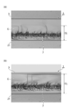
- FIG. 8 (a) and 8 (b) are cross-sectional views for explaining a crack generated from the modified region.
- the left side is a cross-sectional view (crack cross-sectional view along crack C) corresponding to the cross-section along line AA in FIG. 7.
- crack C appears as a crack mark.
- the right-hand side view is a cross-sectional view corresponding to the cross section taken along line BB in FIG.
- the crack C that is generated along with the formation of the modified region 7 is the first scan (that is, when the modified region 7 is formed in a row in the workpiece 1 (that is, This means what occurs when the modified region 7 in the first row is formed).
- FIG. 8B when a plurality of the modified regions 7 are formed in a row, this means what occurs at the multiple (final) scans of the laser light L. This is because, when the modified regions 7 are formed in a plurality of rows, the cracks C are mainly formed at the final scan because the thermal effects and stress accumulated by the irradiation of the laser beam L are easily released at the final scan. This is due to the occurrence.
- the length CL of the crack C (hereinafter referred to as “crack length CL”) means a distance from one end (upper end) to the other end (lower end) of the crack C.
- the crack C extends along the thickness direction of the workpiece 1 from the modified region 7 to be formed.
- the crack C when the formation position of the modified region 7 is close to the back surface 21, it tends to be a back surface side crack extending toward the back surface 21, and the formation position of the modified region 7 is close to the front surface 3. In this case, it tends to be a surface-side crack extending toward the surface 3 side.
- the crack C is a crack (so-called BHC) reaching the back surface 21.
- the crack C here is not included in the modified region 7 because it is not modified.
- the modified region 7 formed by irradiating the laser beam L from the front surface 3 (or the back surface 21) of the workpiece 1 has an elongated shape in the thickness direction of the workpiece 1. It has become.
- the compressive stress F1 and the tensile stress F2 are acting on the upper end and the lower end of the modified region 7. Therefore, when the modified region 1 is formed, the action of the stresses F1 and F2 can be controlled by controlling the pulse width of the laser light L to control the size of the modified region 7.
- the modified region 7 The knowledge that the length of the crack C resulting from the above can be freely controlled is obtained.
- the pulse width of the laser light L is made variable based on the length of the crack C generated from the modified region 7. That is, since the laser light source control unit 102 causes the crack C having a desired length to be generated from the modified region 7, the pulse width is increased (or the crack length is generated as the crack length CL to be generated is increased). The pulse width is controlled so that the pulse width decreases as the length CL decreases.
- the laser light source control unit 102 creates a data table Tb (see FIG. 10) in which “crack length CL”, “thickness of the workpiece 1”, and “pulse width of the laser light L” are associated with each other. Have. Then, the laser light source control unit 102 varies the pulse width of the laser light L according to the data table Tb.
- the variable width of the pulse width by the laser light source control unit 102 is set to 100 nsec to 1500 nsec as a condition for suitably realizing laser processing.
- FIG. 10 is a diagram illustrating an example of a data table.
- the numerical value of the data table Tb indicates “pulse width”, and when “crack length CL” and “thickness of the workpiece 1” are set, they are selected according to these. It is configured to be determined.
- a data string in which the thickness of the workpiece 1 is 300 ⁇ m and 600 ⁇ m indicates data for the second scan.
- the laser light source control unit 102 when “the thickness of the workpiece 1” and “the crack length CL” are input by the laser light source control unit 102, these input values are collated with the data table Tb, A “pulse width” suitable for the length of the crack C to be generated according to the thickness of the workpiece 1 is selected. Then, the laser light source 101 is controlled so that the laser light L is emitted with such a pulse width. That is, the “pulse width” is varied according to the input values of “the thickness of the workpiece 1” and “the crack length CL”.
- the condensing point P position of the laser beam L on the workpiece 1 may also be associated with the data table Tb as another parameter.
- the pulse width is also changed according to the input value of “focusing point P position”, and the position of the stage 111 (or the position of the condensing lens 105) is changed by the stage control unit 115 to the data table Tb. It will be controlled according to.
- the stage controller 115 may separately have a data table Tb related to the position of the condensing point P of the laser light L.
- Tb a data table related to the position of the condensing point P of the laser light L.
- the influence of the adjacent modified region 7 may affect the crack length CL (extension of the crack C), and therefore the position of the condensing point P of the laser beam L is important. Parameter.
- the laser light source control unit 102 associates the “crack length CL”, “thickness of the workpiece 1”, and “pulse width of the laser light L” with each other. Accordingly, the pulse width of the laser light L is varied. That is, the pulse width is varied based on the crack length CL generated from the modified region 7. Therefore, the above knowledge obtained in the pulse width and the crack length CL can be suitably used, and a crack C having a desired length can be generated from the modified region.
- the crack length CL can be increased by increasing the pulse width in order to reduce the number of scans of the laser light L. Further, for example, in the case where a plurality of rows of modified regions 7 are formed in order to improve the processing quality, the crack length CL can be shortened by reducing the pulse width.
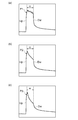
- FIG. 11 is a diagram showing the pulse width of the laser beam.
- the horizontal axis indicates time.
- the pulse width (half-value width) H means a time width from the rising edge Up to the falling edge Dw of the waveform, and changes depending on the current value applied to the laser light source 101, the repetition frequency, and the like. To do. That is, changing the pulse width H includes changing the current value, the repetition frequency, and the like. Note that the pulse width H is FWHM (Full Width at Half Maximum) in the case of Gaussian distribution.
- the pulse waveform P1 shown in FIG. 11 (a) has a substantially rectangular shape
- the pulse waveforms P2 and P3 shown in FIGS. 11 (b) and 11 (c) have a substantially serrated shape having a sharp rise Up.
- the modified region 7 can be accurately formed by the laser light L having any of these pulse waveforms P1 to P3.
- the rise Up is steep (vertical), and it is considered that such a steep rise Up contributes to the formation of the modified region 7 with high accuracy.
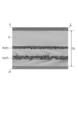
- FIGS. 12 to 14 are cross-sectional views showing examples of workpieces to which laser machining according to the present embodiment has been performed.
- the modified region 7 and the crack C are formed by irradiating the workpiece 1 having a thickness of 100 ⁇ m with the laser beam L from the surface 3 side.
- the pulse width H is set to 150 nsec (E1 in FIG. 10), and the focal point P is located from the surface 3 in order to generate a crack C as a BHC with a crack length CL of 40 ⁇ m.
- the position is 95 ⁇ m.
- the pulse width H is set to 300 nsec (E2 in FIG. 10), and the condensing point P is positioned from the surface 3 in order to generate a crack C as a BHC having a crack length CL of 50 ⁇ m.
- the position is 95 ⁇ m.
- the pulse width H is set to 400 nsec (E3 in FIG. 10), and the condensing point P is located from the surface 3 in order to generate a crack C as a BHC having a crack length CL of 70 ⁇ m.
- the position is 85 ⁇ m.
- the pulse width H is set to 500 nsec (E4 in FIG. 10), and the condensing point P is positioned from the surface 3 in order to generate a crack C as a BHC having a crack length CL of 90 ⁇ m.
- the position is 80 ⁇ m.
- FIG. 13A the pulse width H is set to 400 nsec (E3 in FIG. 10), and the condensing point P is located from the surface 3 in order to generate a crack C as a BHC having a crack length CL of 70 ⁇ m.
- the position is 85 ⁇ m.
- the pulse width H is set to 500 nsec (E4 in FIG. 10)
- the condensing point P is positioned from the surface 3 in order to generate
- the pulse width H is set to 550 nsec so as to generate the crack C as a FC having a crack length CL of 100 ⁇ m (full cut: the crack C extending from the front surface 3 to the back surface 21) (FIG. 10).
- the condensing point P is positioned 60 ⁇ m from the surface 3.
- FIG. 15 is a cross-sectional view showing another example of a workpiece to be processed by laser processing according to the present embodiment.
- the processing object 1 having a thickness of 300 ⁇ m is irradiated with laser light L from the surface 3 side to form modified regions 7a and 7b, and a crack C is formed from the upper modified region 7b.
- the condensing point P is aligned with the position of 240 ⁇ m from the surface 3 to form the modified region 7 a
- the condensing point P is aligned with the position of 155 ⁇ m from the surface 3.
- the modified region 7b is formed.
- the pulse width H is set to 650 nsec in order to generate a crack C as an FC having a crack length CL of 300 ⁇ m (E6 in FIG. 10).
- FIG. 16 is a cross-sectional view showing still another example of the workpiece to which the laser machining according to the present embodiment has been applied.
- the processing object 1 having a thickness of 600 ⁇ m is irradiated with laser light L from the surface 3 side to form modified regions 7a and 7b, and a crack C is formed from the upper modified region 7b.
- the condensing point P is aligned with the position of 591 ⁇ m from the surface 3 to form the modified region 7 a
- the condensing point P is aligned with the position of 541 ⁇ m from the surface 3.
- the modified region 7b is formed.
- the pulse width H is set to 500 nsec in order to generate a crack C as a BHC having a crack length CL of 140 ⁇ m (E7 in FIG. 10).
- the laser processing apparatus which concerns on this invention is not restricted to the laser processing apparatus 100 which concerns on embodiment, In the range which does not change the summary described in each claim It may be modified or applied to others.
- the “crack length CL”, “thickness of the workpiece 1”, and “pulse width of the laser beam L” are associated with each other to configure the data table Tb (see FIG. 10).
- the present invention is not limited to this as long as the pulse width can be varied based on the crack length CL generated from the modified region 7.
- the data table Tb may be configured. That is, the pulse width may be varied only according to the input value related to the crack length CL.
- the laser processing can be carried out with (based on) the crack length CL. Therefore, as shown in FIG. Only the “thickness of the object 1” and the “pulse width of the laser beam L” may be associated with each other to form the data table Tb. That is, the pulse width may be varied only according to the input value relating to the thickness of the workpiece 1.
- a “processing condition” including a processing condition 1 that is a condition that emphasizes quality and a processing condition 2 that is a condition that emphasizes the processing speed is further associated with the data table. Tb may be configured. In this case, it is possible to suitably cope with the manufacture of a plurality of types of mass-produced products.
- the data table Tb is input to the laser light source control unit 102 in advance, but the data table Tb may be read by the laser light source control unit 102 via a line such as the Internet.
- the laser beam L when condensing the laser beam L at a deep position from the laser beam incident surface on which the laser beam L is incident on the workpiece 1, the laser beam L is focused on the condensing point P by increasing the transmittance of the workpiece 1.
- the processing object for example, silicon, glass, LiTaO 3 or sapphire (Al 2 O 3 ) may be included, or may be composed of these.
- SYMBOLS 1 Processing object, 5 ... Planned cutting line, 7, 7a, 7b ... Modified region, 100 ... Laser processing apparatus, 101 ... Laser light source, 102 ... Laser light source control part (control means), C ... Crack, CL ... Crack length (crack length), L ... laser light, P ... condensing point.
Landscapes
- Engineering & Computer Science (AREA)
- Physics & Mathematics (AREA)
- Optics & Photonics (AREA)
- Mechanical Engineering (AREA)
- Plasma & Fusion (AREA)
- Chemical Kinetics & Catalysis (AREA)
- Chemical & Material Sciences (AREA)
- General Chemical & Material Sciences (AREA)
- Oil, Petroleum & Natural Gas (AREA)
- Microelectronics & Electronic Packaging (AREA)
- Power Engineering (AREA)
- Computer Hardware Design (AREA)
- Manufacturing & Machinery (AREA)
- General Physics & Mathematics (AREA)
- Condensed Matter Physics & Semiconductors (AREA)
- Laser Beam Processing (AREA)
- Dicing (AREA)
Abstract
Description
Claims (8)
- 板状の加工対象物の内部に集光点を合わせてレーザ光を照射することにより、前記加工対象物の切断予定ラインに沿って改質領域を前記加工対象物に形成すると共に、前記加工対象物の厚さ方向に沿って延びる亀裂を前記改質領域の形成に伴って該改質領域から生じさせるレーザ加工装置であって、
前記レーザ光を出射するレーザ光源と、
前記レーザ光のパルス幅を制御する制御手段と、を備え、
前記制御手段は、前記改質領域から生じさせる前記亀裂の長さに基づいて前記パルス幅を可変することを特徴とするレーザ加工装置。 - 前記制御手段は、生じさせる前記亀裂の長さを長くするにつれ前記パルス幅が大きくなるように、前記パルス幅を可変することを特徴とする請求項1記載のレーザ加工装置。
- 前記制御手段は、前記亀裂の長さに関する入力値に応じて、前記パルス幅を可変することを特徴とする請求項1記載のレーザ加工装置。
- 前記制御手段は、前記加工対象物の厚さに関する入力値に応じて、前記パルス幅を可変することを特徴とする請求項1記載のレーザ加工装置。
- 前記制御手段は、前記レーザ光の前記集光点の位置に関する入力値に応じて、前記パルス幅を可変することを特徴とする請求項1記載のレーザ加工装置。
- 前記レーザ光源は、ファイバーレーザであることを特徴とする請求項1記載のレーザ加工装置。
- 前記加工対象物は、シリコン基板であり、
前記レーザ光源で出射する前記レーザ光の波長は、1064nm~3000nmであり、
前記制御手段による前記パルス幅の可変幅は、100nsec~1500nsecであることを特徴とする請求項1記載のレーザ加工装置。 - 板状の加工対象物の内部に集光点を合わせてレーザ光を照射することにより、前記加工対象物の切断予定ラインに沿って改質領域を前記加工対象物に形成するレーザ加工方法であって、
前記レーザ光は、略矩形状のパルス波形を有することを特徴とするレーザ加工方法。
Priority Applications (5)
| Application Number | Priority Date | Filing Date | Title |
|---|---|---|---|
| KR1020117013931A KR101769158B1 (ko) | 2009-04-07 | 2010-03-29 | 레이저 가공 장치 및 레이저 가공 방법 |
| JP2011508335A JP5639997B2 (ja) | 2009-04-07 | 2010-03-29 | レーザ加工装置 |
| EP10761616.1A EP2418041B1 (en) | 2009-04-07 | 2010-03-29 | Laser machining device and laser machining method |
| CN201080008067.XA CN102317030B (zh) | 2009-04-07 | 2010-03-29 | 激光加工装置以及激光加工方法 |
| US13/262,995 US9035216B2 (en) | 2009-04-07 | 2010-03-29 | Method and device for controlling interior fractures by controlling the laser pulse width |
Applications Claiming Priority (2)
| Application Number | Priority Date | Filing Date | Title |
|---|---|---|---|
| JP2009092846 | 2009-04-07 | ||
| JP2009-092846 | 2009-04-07 |
Publications (1)
| Publication Number | Publication Date |
|---|---|
| WO2010116917A1 true WO2010116917A1 (ja) | 2010-10-14 |
Family
ID=42936202
Family Applications (1)
| Application Number | Title | Priority Date | Filing Date |
|---|---|---|---|
| PCT/JP2010/055585 WO2010116917A1 (ja) | 2009-04-07 | 2010-03-29 | レーザ加工装置及びレーザ加工方法 |
Country Status (7)
| Country | Link |
|---|---|
| US (1) | US9035216B2 (ja) |
| EP (1) | EP2418041B1 (ja) |
| JP (2) | JP5639997B2 (ja) |
| KR (1) | KR101769158B1 (ja) |
| CN (1) | CN102317030B (ja) |
| TW (1) | TWI593497B (ja) |
| WO (1) | WO2010116917A1 (ja) |
Cited By (16)
| Publication number | Priority date | Publication date | Assignee | Title |
|---|---|---|---|---|
| CN102152003A (zh) * | 2011-02-24 | 2011-08-17 | 华中科技大学 | 双激光束分离光学晶体方法及装置 |
| WO2011152230A1 (ja) * | 2010-06-02 | 2011-12-08 | 浜松ホトニクス株式会社 | レーザ加工方法 |
| JP2012169361A (ja) * | 2011-02-10 | 2012-09-06 | Saitama Univ | 基板加工方法及び基板 |
| JP2013128088A (ja) * | 2011-11-18 | 2013-06-27 | Hamamatsu Photonics Kk | レーザ加工方法及びレーザ加工装置 |
| JP2014107485A (ja) * | 2012-11-29 | 2014-06-09 | Mitsuboshi Diamond Industrial Co Ltd | パターン付き基板の分割方法 |
| CN103862180A (zh) * | 2014-01-29 | 2014-06-18 | 苏州兰叶光电科技有限公司 | 玻璃盖片激光划片装置 |
| JP2015012015A (ja) * | 2013-06-26 | 2015-01-19 | 株式会社ディスコ | ウェーハの加工方法 |
| JP2016042514A (ja) * | 2014-08-15 | 2016-03-31 | 株式会社ディスコ | ウエーハの加工方法 |
| JP2016042515A (ja) * | 2014-08-15 | 2016-03-31 | 株式会社ディスコ | ウエーハの加工方法 |
| JP2016072278A (ja) * | 2014-09-26 | 2016-05-09 | 株式会社ディスコ | ウエーハの加工方法 |
| US9821408B2 (en) | 2011-09-16 | 2017-11-21 | Hamamatsu Photonics K.K. | Laser machining method and laser machining device |
| JP2018117037A (ja) * | 2017-01-18 | 2018-07-26 | 株式会社ディスコ | 加工方法 |
| JP2021048235A (ja) * | 2019-09-18 | 2021-03-25 | 浜松ホトニクス株式会社 | 検査装置及び検査方法 |
| JP2021048236A (ja) * | 2019-09-18 | 2021-03-25 | 浜松ホトニクス株式会社 | 検査装置及び検査方法 |
| WO2021177376A1 (ja) * | 2020-03-06 | 2021-09-10 | 浜松ホトニクス株式会社 | 検査装置及び処理システム |
| CN114096373A (zh) * | 2019-07-18 | 2022-02-25 | 东京毅力科创株式会社 | 处理装置和处理方法 |
Families Citing this family (13)
| Publication number | Priority date | Publication date | Assignee | Title |
|---|---|---|---|---|
| JP2011201759A (ja) * | 2010-03-05 | 2011-10-13 | Namiki Precision Jewel Co Ltd | 多層膜付き単結晶基板、多層膜付き単結晶基板の製造方法および素子製造方法 |
| KR101361777B1 (ko) * | 2012-04-03 | 2014-02-13 | 주식회사 이오테크닉스 | 레이저 가공방법 |
| JP6064519B2 (ja) * | 2012-10-29 | 2017-01-25 | 三星ダイヤモンド工業株式会社 | レーザー加工装置、および、パターン付き基板の加工条件設定方法 |
| JP6208430B2 (ja) * | 2013-01-25 | 2017-10-04 | 株式会社ディスコ | レーザー加工方法 |
| US9102007B2 (en) * | 2013-08-02 | 2015-08-11 | Rofin-Sinar Technologies Inc. | Method and apparatus for performing laser filamentation within transparent materials |
| JP6241174B2 (ja) * | 2013-09-25 | 2017-12-06 | 三星ダイヤモンド工業株式会社 | レーザー加工装置、および、パターン付き基板の加工条件設定方法 |
| JP2016076521A (ja) * | 2014-10-02 | 2016-05-12 | 株式会社ディスコ | ウエーハの加工方法 |
| JP6605277B2 (ja) * | 2015-09-29 | 2019-11-13 | 浜松ホトニクス株式会社 | レーザ加工方法及びレーザ加工装置 |
| JP7307534B2 (ja) * | 2018-10-04 | 2023-07-12 | 浜松ホトニクス株式会社 | レーザ加工方法、半導体デバイス製造方法及び検査装置 |
| US11024501B2 (en) | 2018-12-29 | 2021-06-01 | Cree, Inc. | Carrier-assisted method for parting crystalline material along laser damage region |
| US10576585B1 (en) | 2018-12-29 | 2020-03-03 | Cree, Inc. | Laser-assisted method for parting crystalline material |
| US10562130B1 (en) | 2018-12-29 | 2020-02-18 | Cree, Inc. | Laser-assisted method for parting crystalline material |
| US10611052B1 (en) | 2019-05-17 | 2020-04-07 | Cree, Inc. | Silicon carbide wafers with relaxed positive bow and related methods |
Citations (7)
| Publication number | Priority date | Publication date | Assignee | Title |
|---|---|---|---|---|
| JP2005057257A (ja) * | 2003-07-18 | 2005-03-03 | Hamamatsu Photonics Kk | レーザ加工方法、レーザ加工装置、及び加工生産物 |
| JP2006108459A (ja) | 2004-10-07 | 2006-04-20 | Disco Abrasive Syst Ltd | シリコンウエーハのレーザー加工方法およびレーザー加工装置 |
| JP2007079161A (ja) * | 2005-09-14 | 2007-03-29 | Toyota Motor Corp | 超短パルスレーザー加工用光学系、材料微細加工方法、及び微細加工装置 |
| JP2008087053A (ja) * | 2006-10-03 | 2008-04-17 | Hamamatsu Photonics Kk | レーザ加工方法 |
| JP2008212998A (ja) * | 2007-03-06 | 2008-09-18 | Seiko Epson Corp | レーザ加工装置、レーザ加工方法、基板の分割方法、及び電気光学装置の製造方法 |
| JP2008276057A (ja) * | 2007-05-02 | 2008-11-13 | Active Inc | 液晶表示装置の透明電極膜加工方法 |
| JP2009023215A (ja) * | 2007-07-19 | 2009-02-05 | Panasonic Electric Works Co Ltd | 積層体の割断方法 |
Family Cites Families (64)
| Publication number | Priority date | Publication date | Assignee | Title |
|---|---|---|---|---|
| US4546231A (en) | 1983-11-14 | 1985-10-08 | Group Ii Manufacturing Ltd. | Creation of a parting zone in a crystal structure |
| US5073687A (en) * | 1989-06-22 | 1991-12-17 | Canon Kabushiki Kaisha | Method and apparatus for working print board by laser |
| KR0171947B1 (ko) | 1995-12-08 | 1999-03-20 | 김주용 | 반도체소자 제조를 위한 노광 방법 및 그를 이용한 노광장치 |
| JP2000288758A (ja) * | 1999-03-31 | 2000-10-17 | Hitachi Ltd | レーザ切断装置 |
| US6417485B1 (en) * | 2000-05-30 | 2002-07-09 | Igor Troitski | Method and laser system controlling breakdown process development and space structure of laser radiation for production of high quality laser-induced damage images |
| JP4659300B2 (ja) | 2000-09-13 | 2011-03-30 | 浜松ホトニクス株式会社 | レーザ加工方法及び半導体チップの製造方法 |
| TWI326626B (en) | 2002-03-12 | 2010-07-01 | Hamamatsu Photonics Kk | Laser processing method |
| DE60335538D1 (de) | 2002-03-12 | 2011-02-10 | Hamamatsu Photonics Kk | Verfahren zum schneiden eines bearbeiteten objekts |
| CN100355032C (zh) | 2002-03-12 | 2007-12-12 | 浜松光子学株式会社 | 基板的分割方法 |
| JP3667705B2 (ja) * | 2002-03-26 | 2005-07-06 | 住友重機械工業株式会社 | レーザ加工装置及び加工方法 |
| TWI520269B (zh) | 2002-12-03 | 2016-02-01 | Hamamatsu Photonics Kk | Cutting method of semiconductor substrate |
| ES2381254T3 (es) | 2002-12-05 | 2012-05-24 | Hamamatsu Photonics K.K. | Dispositivos de procesamiento con láser |
| JP2004188422A (ja) | 2002-12-06 | 2004-07-08 | Hamamatsu Photonics Kk | レーザ加工装置及びレーザ加工方法 |
| JP2004268103A (ja) | 2003-03-10 | 2004-09-30 | Hamamatsu Photonics Kk | レーザ加工方法 |
| FR2852250B1 (fr) | 2003-03-11 | 2009-07-24 | Jean Luc Jouvin | Fourreau de protection pour canule, un ensemble d'injection comportant un tel fourreau et aiguille equipee d'un tel fourreau |
| EP1609559B1 (en) | 2003-03-12 | 2007-08-08 | Hamamatsu Photonics K. K. | Laser beam machining method |
| KR101193723B1 (ko) | 2003-07-18 | 2012-10-22 | 하마마츠 포토닉스 가부시키가이샤 | 반도체 기판, 반도체 기판의 절단방법 및 가공대상물의 절단방법 |
| JP4563097B2 (ja) | 2003-09-10 | 2010-10-13 | 浜松ホトニクス株式会社 | 半導体基板の切断方法 |
| JP2005086175A (ja) | 2003-09-11 | 2005-03-31 | Hamamatsu Photonics Kk | 半導体薄膜の製造方法、半導体薄膜、半導体薄膜チップ、電子管、及び光検出素子 |
| GB0328370D0 (en) * | 2003-12-05 | 2004-01-14 | Southampton Photonics Ltd | Apparatus for providing optical radiation |
| EP1705764B1 (en) | 2004-01-07 | 2012-11-14 | Hamamatsu Photonics K. K. | Semiconductor light-emitting device and its manufacturing method |
| JP4598407B2 (ja) | 2004-01-09 | 2010-12-15 | 浜松ホトニクス株式会社 | レーザ加工方法及びレーザ加工装置 |
| JP4601965B2 (ja) | 2004-01-09 | 2010-12-22 | 浜松ホトニクス株式会社 | レーザ加工方法及びレーザ加工装置 |
| JP4509578B2 (ja) | 2004-01-09 | 2010-07-21 | 浜松ホトニクス株式会社 | レーザ加工方法及びレーザ加工装置 |
| JP4348199B2 (ja) * | 2004-01-16 | 2009-10-21 | 日立ビアメカニクス株式会社 | レーザ加工方法およびレーザ加工装置 |
| JP2005268752A (ja) * | 2004-02-19 | 2005-09-29 | Canon Inc | レーザ割断方法、被割断部材および半導体素子チップ |
| ATE556807T1 (de) | 2004-03-30 | 2012-05-15 | Hamamatsu Photonics Kk | Laserverarbeitungsverfahren |
| CN1938827B (zh) | 2004-03-30 | 2010-05-26 | 浜松光子学株式会社 | 激光加工方法及半导体芯片 |
| JP4536407B2 (ja) | 2004-03-30 | 2010-09-01 | 浜松ホトニクス株式会社 | レーザ加工方法及び加工対象物 |
| US7804043B2 (en) * | 2004-06-15 | 2010-09-28 | Laserfacturing Inc. | Method and apparatus for dicing of thin and ultra thin semiconductor wafer using ultrafast pulse laser |
| JP4634089B2 (ja) | 2004-07-30 | 2011-02-16 | 浜松ホトニクス株式会社 | レーザ加工方法 |
| KR101109860B1 (ko) | 2004-08-06 | 2012-02-21 | 하마마츠 포토닉스 가부시키가이샤 | 레이저 가공 방법, 가공 대상물 절단 방법 및 반도체 장치 |
| WO2006037114A2 (en) * | 2004-09-28 | 2006-04-06 | Hitachi Via Mechanics, Ltd | Fiber laser based production of laser drilled microvias for multi-layer drilling, dicing, trimming or milling applications |
| JP4754801B2 (ja) | 2004-10-13 | 2011-08-24 | 浜松ホトニクス株式会社 | レーザ加工方法 |
| JP4917257B2 (ja) | 2004-11-12 | 2012-04-18 | 浜松ホトニクス株式会社 | レーザ加工方法 |
| JP4781661B2 (ja) | 2004-11-12 | 2011-09-28 | 浜松ホトニクス株式会社 | レーザ加工方法 |
| US8093530B2 (en) * | 2004-11-19 | 2012-01-10 | Canon Kabushiki Kaisha | Laser cutting apparatus and laser cutting method |
| JP4198123B2 (ja) | 2005-03-22 | 2008-12-17 | 浜松ホトニクス株式会社 | レーザ加工方法 |
| JP4776994B2 (ja) | 2005-07-04 | 2011-09-21 | 浜松ホトニクス株式会社 | 加工対象物切断方法 |
| JP4395110B2 (ja) * | 2005-07-29 | 2010-01-06 | 東レエンジニアリング株式会社 | 透明材料へのマーキング方法およびこれを用いた装置 |
| JP4749799B2 (ja) | 2005-08-12 | 2011-08-17 | 浜松ホトニクス株式会社 | レーザ加工方法 |
| JP4762653B2 (ja) | 2005-09-16 | 2011-08-31 | 浜松ホトニクス株式会社 | レーザ加工方法及びレーザ加工装置 |
| JP4237745B2 (ja) | 2005-11-18 | 2009-03-11 | 浜松ホトニクス株式会社 | レーザ加工方法 |
| JP4907965B2 (ja) | 2005-11-25 | 2012-04-04 | 浜松ホトニクス株式会社 | レーザ加工方法 |
| JP4804911B2 (ja) | 2005-12-22 | 2011-11-02 | 浜松ホトニクス株式会社 | レーザ加工装置 |
| JP4907984B2 (ja) | 2005-12-27 | 2012-04-04 | 浜松ホトニクス株式会社 | レーザ加工方法及び半導体チップ |
| JP4322881B2 (ja) * | 2006-03-14 | 2009-09-02 | 浜松ホトニクス株式会社 | レーザ加工方法及びレーザ加工装置 |
| US20070228023A1 (en) * | 2006-03-30 | 2007-10-04 | Klaus Kleine | Pulsed Synchronized Laser Cutting of Stents |
| US7897487B2 (en) | 2006-07-03 | 2011-03-01 | Hamamatsu Photonics K.K. | Laser processing method and chip |
| JP5183892B2 (ja) | 2006-07-03 | 2013-04-17 | 浜松ホトニクス株式会社 | レーザ加工方法 |
| US7732731B2 (en) | 2006-09-15 | 2010-06-08 | Gsi Group Corporation | Method and system for laser processing targets of different types on a workpiece |
| CN101516566B (zh) | 2006-09-19 | 2012-05-09 | 浜松光子学株式会社 | 激光加工方法和激光加工装置 |
| JP4954653B2 (ja) | 2006-09-19 | 2012-06-20 | 浜松ホトニクス株式会社 | レーザ加工方法 |
| JP5101073B2 (ja) | 2006-10-02 | 2012-12-19 | 浜松ホトニクス株式会社 | レーザ加工装置 |
| JP5132911B2 (ja) | 2006-10-03 | 2013-01-30 | 浜松ホトニクス株式会社 | レーザ加工方法 |
| CN101522362B (zh) | 2006-10-04 | 2012-11-14 | 浜松光子学株式会社 | 激光加工方法 |
| JP5336054B2 (ja) | 2007-07-18 | 2013-11-06 | 浜松ホトニクス株式会社 | 加工情報供給装置を備える加工情報供給システム |
| JP4402708B2 (ja) | 2007-08-03 | 2010-01-20 | 浜松ホトニクス株式会社 | レーザ加工方法、レーザ加工装置及びその製造方法 |
| JP5225639B2 (ja) | 2007-09-06 | 2013-07-03 | 浜松ホトニクス株式会社 | 半導体レーザ素子の製造方法 |
| JP5342772B2 (ja) | 2007-10-12 | 2013-11-13 | 浜松ホトニクス株式会社 | 加工対象物切断方法 |
| JP5449665B2 (ja) | 2007-10-30 | 2014-03-19 | 浜松ホトニクス株式会社 | レーザ加工方法 |
| JP5054496B2 (ja) | 2007-11-30 | 2012-10-24 | 浜松ホトニクス株式会社 | 加工対象物切断方法 |
| JP5134928B2 (ja) | 2007-11-30 | 2013-01-30 | 浜松ホトニクス株式会社 | 加工対象物研削方法 |
| JP5241525B2 (ja) | 2009-01-09 | 2013-07-17 | 浜松ホトニクス株式会社 | レーザ加工装置 |
-
2010
- 2010-03-29 EP EP10761616.1A patent/EP2418041B1/en active Active
- 2010-03-29 JP JP2011508335A patent/JP5639997B2/ja active Active
- 2010-03-29 US US13/262,995 patent/US9035216B2/en active Active
- 2010-03-29 WO PCT/JP2010/055585 patent/WO2010116917A1/ja active Application Filing
- 2010-03-29 CN CN201080008067.XA patent/CN102317030B/zh active Active
- 2010-03-29 KR KR1020117013931A patent/KR101769158B1/ko active Active
- 2010-04-06 TW TW099110584A patent/TWI593497B/zh active
-
2014
- 2014-04-22 JP JP2014088207A patent/JP2014176901A/ja active Pending
Patent Citations (7)
| Publication number | Priority date | Publication date | Assignee | Title |
|---|---|---|---|---|
| JP2005057257A (ja) * | 2003-07-18 | 2005-03-03 | Hamamatsu Photonics Kk | レーザ加工方法、レーザ加工装置、及び加工生産物 |
| JP2006108459A (ja) | 2004-10-07 | 2006-04-20 | Disco Abrasive Syst Ltd | シリコンウエーハのレーザー加工方法およびレーザー加工装置 |
| JP2007079161A (ja) * | 2005-09-14 | 2007-03-29 | Toyota Motor Corp | 超短パルスレーザー加工用光学系、材料微細加工方法、及び微細加工装置 |
| JP2008087053A (ja) * | 2006-10-03 | 2008-04-17 | Hamamatsu Photonics Kk | レーザ加工方法 |
| JP2008212998A (ja) * | 2007-03-06 | 2008-09-18 | Seiko Epson Corp | レーザ加工装置、レーザ加工方法、基板の分割方法、及び電気光学装置の製造方法 |
| JP2008276057A (ja) * | 2007-05-02 | 2008-11-13 | Active Inc | 液晶表示装置の透明電極膜加工方法 |
| JP2009023215A (ja) * | 2007-07-19 | 2009-02-05 | Panasonic Electric Works Co Ltd | 積層体の割断方法 |
Non-Patent Citations (1)
| Title |
|---|
| See also references of EP2418041A4 |
Cited By (28)
| Publication number | Priority date | Publication date | Assignee | Title |
|---|---|---|---|---|
| US9409256B2 (en) | 2010-06-02 | 2016-08-09 | Hamamatsu Photonics K.K. | Laser processing method |
| WO2011152230A1 (ja) * | 2010-06-02 | 2011-12-08 | 浜松ホトニクス株式会社 | レーザ加工方法 |
| JP2012169361A (ja) * | 2011-02-10 | 2012-09-06 | Saitama Univ | 基板加工方法及び基板 |
| CN102152003A (zh) * | 2011-02-24 | 2011-08-17 | 华中科技大学 | 双激光束分离光学晶体方法及装置 |
| TWI625186B (zh) * | 2011-09-16 | 2018-06-01 | Hamamatsu Photonics Kk | Laser processing method and laser processing device |
| US9821408B2 (en) | 2011-09-16 | 2017-11-21 | Hamamatsu Photonics K.K. | Laser machining method and laser machining device |
| JP2013128088A (ja) * | 2011-11-18 | 2013-06-27 | Hamamatsu Photonics Kk | レーザ加工方法及びレーザ加工装置 |
| JP2014107485A (ja) * | 2012-11-29 | 2014-06-09 | Mitsuboshi Diamond Industrial Co Ltd | パターン付き基板の分割方法 |
| JP2015012015A (ja) * | 2013-06-26 | 2015-01-19 | 株式会社ディスコ | ウェーハの加工方法 |
| CN103862180A (zh) * | 2014-01-29 | 2014-06-18 | 苏州兰叶光电科技有限公司 | 玻璃盖片激光划片装置 |
| JP2016042515A (ja) * | 2014-08-15 | 2016-03-31 | 株式会社ディスコ | ウエーハの加工方法 |
| JP2016042514A (ja) * | 2014-08-15 | 2016-03-31 | 株式会社ディスコ | ウエーハの加工方法 |
| JP2016072278A (ja) * | 2014-09-26 | 2016-05-09 | 株式会社ディスコ | ウエーハの加工方法 |
| JP2018117037A (ja) * | 2017-01-18 | 2018-07-26 | 株式会社ディスコ | 加工方法 |
| CN114096373A (zh) * | 2019-07-18 | 2022-02-25 | 东京毅力科创株式会社 | 处理装置和处理方法 |
| CN114096373B (zh) * | 2019-07-18 | 2023-12-01 | 东京毅力科创株式会社 | 处理装置和处理方法 |
| JP2021048235A (ja) * | 2019-09-18 | 2021-03-25 | 浜松ホトニクス株式会社 | 検査装置及び検査方法 |
| WO2021054372A1 (ja) * | 2019-09-18 | 2021-03-25 | 浜松ホトニクス株式会社 | 検査装置及び検査方法 |
| JP2021048236A (ja) * | 2019-09-18 | 2021-03-25 | 浜松ホトニクス株式会社 | 検査装置及び検査方法 |
| US20220331908A1 (en) * | 2019-09-18 | 2022-10-20 | Hamamatsu Photonics K.K. | Inspection device and inspection method |
| JP7305495B2 (ja) | 2019-09-18 | 2023-07-10 | 浜松ホトニクス株式会社 | 検査装置及び検査方法 |
| WO2021054353A1 (ja) * | 2019-09-18 | 2021-03-25 | 浜松ホトニクス株式会社 | 検査装置及び検査方法 |
| JP7391583B2 (ja) | 2019-09-18 | 2023-12-05 | 浜松ホトニクス株式会社 | 検査装置及び検査方法 |
| US12023761B2 (en) | 2019-09-18 | 2024-07-02 | Hamamatsu Photonics K.K. | Inspection device and inspection method |
| WO2021177376A1 (ja) * | 2020-03-06 | 2021-09-10 | 浜松ホトニクス株式会社 | 検査装置及び処理システム |
| JP2021141249A (ja) * | 2020-03-06 | 2021-09-16 | 浜松ホトニクス株式会社 | 検査装置及び処理システム |
| JP7385504B2 (ja) | 2020-03-06 | 2023-11-22 | 浜松ホトニクス株式会社 | 検査装置及び処理システム |
| US12272577B2 (en) | 2020-03-06 | 2025-04-08 | Hamamatsu Photonics K.K. | Inspection device and processing system |
Also Published As
| Publication number | Publication date |
|---|---|
| CN102317030B (zh) | 2014-08-20 |
| JPWO2010116917A1 (ja) | 2012-10-18 |
| US20120103948A1 (en) | 2012-05-03 |
| CN102317030A (zh) | 2012-01-11 |
| JP5639997B2 (ja) | 2014-12-10 |
| KR101769158B1 (ko) | 2017-08-17 |
| JP2014176901A (ja) | 2014-09-25 |
| TW201043382A (en) | 2010-12-16 |
| EP2418041B1 (en) | 2024-09-18 |
| EP2418041A4 (en) | 2017-06-21 |
| US9035216B2 (en) | 2015-05-19 |
| KR20120005432A (ko) | 2012-01-16 |
| TWI593497B (zh) | 2017-08-01 |
| EP2418041A1 (en) | 2012-02-15 |
Similar Documents
| Publication | Publication Date | Title |
|---|---|---|
| JP5639997B2 (ja) | レーザ加工装置 | |
| JP5449665B2 (ja) | レーザ加工方法 | |
| JP5491761B2 (ja) | レーザ加工装置 | |
| JP5597052B2 (ja) | レーザ加工方法 | |
| JP4322881B2 (ja) | レーザ加工方法及びレーザ加工装置 | |
| JP5597051B2 (ja) | レーザ加工方法 | |
| JP5312761B2 (ja) | 切断用加工方法 | |
| JP5089735B2 (ja) | レーザ加工装置 | |
| JP4584322B2 (ja) | レーザ加工方法 | |
| WO2012096094A1 (ja) | レーザ加工方法 | |
| WO2012096096A1 (ja) | レーザ加工方法 | |
| WO2008035679A1 (fr) | Procédé de traitement au laser et appareil de traitement au laser | |
| WO2012096097A1 (ja) | レーザ加工方法 | |
| TWI515071B (zh) | Laser processing method | |
| KR20120098869A (ko) | 레이저 가공과 스크라이빙 시스템 및 방법 | |
| JP2008012542A (ja) | レーザ加工方法 | |
| WO2012096092A1 (ja) | レーザ加工方法 | |
| JP5117806B2 (ja) | レーザ加工方法及びレーザ加工装置 | |
| JP2008100284A (ja) | レーザ加工方法及びレーザ加工装置 | |
| JP2010239157A (ja) | レーザ切断方法 | |
| WO2012096093A1 (ja) | レーザ加工方法 | |
| KR101164418B1 (ko) | 펨토초 펄스 레이저의 비선형 초점이동을 통한 절단방법 | |
| JP5613809B2 (ja) | レーザ切断方法およびレーザ加工装置 | |
| JP6957187B2 (ja) | チップの製造方法、及び、シリコンチップ |
Legal Events
| Date | Code | Title | Description |
|---|---|---|---|
| WWE | Wipo information: entry into national phase |
Ref document number: 201080008067.X Country of ref document: CN |
|
| 121 | Ep: the epo has been informed by wipo that ep was designated in this application |
Ref document number: 10761616 Country of ref document: EP Kind code of ref document: A1 |
|
| ENP | Entry into the national phase |
Ref document number: 2011508335 Country of ref document: JP Kind code of ref document: A |
|
| ENP | Entry into the national phase |
Ref document number: 20117013931 Country of ref document: KR Kind code of ref document: A |
|
| NENP | Non-entry into the national phase |
Ref country code: DE |
|
| WWE | Wipo information: entry into national phase |
Ref document number: 2010761616 Country of ref document: EP |
|
| WWE | Wipo information: entry into national phase |
Ref document number: 13262995 Country of ref document: US |