WO2010116728A1 - 型およびその製造方法 - Google Patents
型およびその製造方法 Download PDFInfo
- Publication number
- WO2010116728A1 WO2010116728A1 PCT/JP2010/002518 JP2010002518W WO2010116728A1 WO 2010116728 A1 WO2010116728 A1 WO 2010116728A1 JP 2010002518 W JP2010002518 W JP 2010002518W WO 2010116728 A1 WO2010116728 A1 WO 2010116728A1
- Authority
- WO
- WIPO (PCT)
- Prior art keywords
- layer
- aluminum
- mold
- buffer layer
- inorganic
- Prior art date
- Legal status (The legal status is an assumption and is not a legal conclusion. Google has not performed a legal analysis and makes no representation as to the accuracy of the status listed.)
- Ceased
Links
Images


Classifications
-
- G—PHYSICS
- G02—OPTICS
- G02B—OPTICAL ELEMENTS, SYSTEMS OR APPARATUS
- G02B1/00—Optical elements characterised by the material of which they are made; Optical coatings for optical elements
- G02B1/10—Optical coatings produced by application to, or surface treatment of, optical elements
- G02B1/11—Anti-reflection coatings
- G02B1/118—Anti-reflection coatings having sub-optical wavelength surface structures designed to provide an enhanced transmittance, e.g. moth-eye structures
-
- B—PERFORMING OPERATIONS; TRANSPORTING
- B29—WORKING OF PLASTICS; WORKING OF SUBSTANCES IN A PLASTIC STATE IN GENERAL
- B29C—SHAPING OR JOINING OF PLASTICS; SHAPING OF MATERIAL IN A PLASTIC STATE, NOT OTHERWISE PROVIDED FOR; AFTER-TREATMENT OF THE SHAPED PRODUCTS, e.g. REPAIRING
- B29C33/00—Moulds or cores; Details thereof or accessories therefor
- B29C33/38—Moulds or cores; Details thereof or accessories therefor characterised by the material or the manufacturing process
-
- B—PERFORMING OPERATIONS; TRANSPORTING
- B29—WORKING OF PLASTICS; WORKING OF SUBSTANCES IN A PLASTIC STATE IN GENERAL
- B29C—SHAPING OR JOINING OF PLASTICS; SHAPING OF MATERIAL IN A PLASTIC STATE, NOT OTHERWISE PROVIDED FOR; AFTER-TREATMENT OF THE SHAPED PRODUCTS, e.g. REPAIRING
- B29C33/00—Moulds or cores; Details thereof or accessories therefor
- B29C33/38—Moulds or cores; Details thereof or accessories therefor characterised by the material or the manufacturing process
- B29C33/3814—Porous moulds
-
- B—PERFORMING OPERATIONS; TRANSPORTING
- B29—WORKING OF PLASTICS; WORKING OF SUBSTANCES IN A PLASTIC STATE IN GENERAL
- B29C—SHAPING OR JOINING OF PLASTICS; SHAPING OF MATERIAL IN A PLASTIC STATE, NOT OTHERWISE PROVIDED FOR; AFTER-TREATMENT OF THE SHAPED PRODUCTS, e.g. REPAIRING
- B29C33/00—Moulds or cores; Details thereof or accessories therefor
- B29C33/42—Moulds or cores; Details thereof or accessories therefor characterised by the shape of the moulding surface, e.g. ribs or grooves
- B29C33/424—Moulding surfaces provided with means for marking or patterning
-
- B—PERFORMING OPERATIONS; TRANSPORTING
- B29—WORKING OF PLASTICS; WORKING OF SUBSTANCES IN A PLASTIC STATE IN GENERAL
- B29C—SHAPING OR JOINING OF PLASTICS; SHAPING OF MATERIAL IN A PLASTIC STATE, NOT OTHERWISE PROVIDED FOR; AFTER-TREATMENT OF THE SHAPED PRODUCTS, e.g. REPAIRING
- B29C33/00—Moulds or cores; Details thereof or accessories therefor
- B29C33/56—Coatings, e.g. enameled or galvanised; Releasing, lubricating or separating agents
-
- C—CHEMISTRY; METALLURGY
- C25—ELECTROLYTIC OR ELECTROPHORETIC PROCESSES; APPARATUS THEREFOR
- C25D—PROCESSES FOR THE ELECTROLYTIC OR ELECTROPHORETIC PRODUCTION OF COATINGS; ELECTROFORMING; APPARATUS THEREFOR
- C25D11/00—Electrolytic coating by surface reaction, i.e. forming conversion layers
- C25D11/02—Anodisation
- C25D11/04—Anodisation of aluminium or alloys based thereon
- C25D11/12—Anodising more than once, e.g. in different baths
-
- C—CHEMISTRY; METALLURGY
- C25—ELECTROLYTIC OR ELECTROPHORETIC PROCESSES; APPARATUS THEREFOR
- C25D—PROCESSES FOR THE ELECTROLYTIC OR ELECTROPHORETIC PRODUCTION OF COATINGS; ELECTROFORMING; APPARATUS THEREFOR
- C25D11/00—Electrolytic coating by surface reaction, i.e. forming conversion layers
- C25D11/02—Anodisation
- C25D11/04—Anodisation of aluminium or alloys based thereon
- C25D11/18—After-treatment, e.g. pore-sealing
- C25D11/24—Chemical after-treatment
Definitions
- the present invention relates to a mold and a method for manufacturing the mold.
- the “mold” here includes molds used in various processing methods (stamping and casting), and is sometimes referred to as a stamper. It can also be used for printing (including nanoprinting).
- An optical element such as a display device or a camera lens used for a television or a mobile phone is usually provided with an antireflection technique in order to reduce surface reflection and increase light transmission.
- an antireflection technique in order to reduce surface reflection and increase light transmission. For example, when light passes through the interface of a medium with a different refractive index, such as when light enters the interface between air and glass, the amount of transmitted light is reduced due to Fresnel reflection, and visibility is reduced. is there.
- This method utilizes the principle of a so-called moth-eye structure, and the refractive index for light incident on the substrate is determined from the refractive index of the incident medium along the depth direction of the irregularities, to the refractive index of the substrate.
- the reflection in the wavelength region where the reflection is desired to be prevented is suppressed by continuously changing the wavelength.
- the moth-eye structure has an advantage that it can exhibit an antireflection effect with a small incident angle dependency over a wide wavelength range, can be applied to many materials, and can form an uneven pattern directly on a substrate. As a result, a low-cost and high-performance antireflection film (or antireflection surface) can be provided.
- Patent Documents 2 to 4 As a method for producing a moth-eye structure, a method using an anodized porous alumina layer obtained by anodizing aluminum is attracting attention (Patent Documents 2 to 4).
- anodized porous alumina layer obtained by anodizing aluminum will be briefly described.
- a method for producing a porous structure using anodization has attracted attention as a simple method capable of forming regularly ordered nano-sized cylindrical pores (fine concave portions).
- an acidic or alkaline electrolyte such as sulfuric acid, oxalic acid, or phosphoric acid
- a voltage is applied using the aluminum substrate as an anode
- oxidation and dissolution proceed simultaneously on the surface of the aluminum substrate.
- An oxide film having pores can be formed. These cylindrical pores are oriented perpendicular to the oxide film and exhibit self-organized regularity under certain conditions (voltage, type of electrolyte, temperature, etc.). Is expected.
- the porous alumina layer formed under specific conditions takes an array in which almost regular hexagonal cells are two-dimensionally filled with the highest density when viewed from the direction perpendicular to the film surface.
- Each cell has a pore in the center, and the arrangement of the pores has periodicity.
- the cell is formed as a result of local dissolution and growth of the film, and dissolution and growth of the film proceed simultaneously at the bottom of the pores called a barrier layer.
- the cell size that is, the distance between adjacent pores (center-to-center distance) corresponds to approximately twice the thickness of the barrier layer and is approximately proportional to the voltage during anodization.
- the diameter of the pores depends on the type, concentration, temperature, etc.
- the pores of such porous alumina have an arrangement with high regularity (having periodicity) under a specific condition, an arrangement with irregularity to some extent or an irregularity (having no periodicity) depending on the conditions. ).
- Patent Document 2 discloses a method of forming an antireflection film (antireflection surface) using a stamper having an anodized porous alumina film on the surface.
- Patent Document 3 discloses a technique for forming a tapered concave portion in which the pore diameter continuously changes by repeating anodization of aluminum and pore diameter enlargement processing.
- Patent Document 4 a technique for forming an antireflection film using an alumina layer in which fine concave portions have stepped side surfaces.
- an antireflection film (antireflection surface) is provided by providing a concavo-convex structure (macro structure) larger than the moth eye structure in addition to the moth eye structure (micro structure). ) Can be given an anti-glare (anti-glare) function.
- the two-dimensional size of the projections that form the projections and depressions that exhibit the antiglare function is 1 ⁇ m or more and less than 100 ⁇ m.
- a mold for forming a moth-eye structure on the surface (hereinafter referred to as “moth-eye mold”) can be easily manufactured.
- the surface of an anodized aluminum film is used as it is as a mold, the effect of reducing the manufacturing cost is great.
- the surface structure of the moth-eye mold that can form the moth-eye structure is referred to as an “inverted moth-eye structure”.
- the above moth-eye mold is formed on an aluminum substrate represented by a substrate formed of aluminum or a cylinder formed of aluminum, or a support formed of another material typified by a glass substrate. It can be manufactured using an aluminum film.
- the aluminum film partially an anodized film
- the glass substrate were used in the anodizing process or etching process.
- the adhesiveness with was lowered. This problem was significant when a glass substrate containing alkali metal (soda lime glass) was used.
- a plastic film is used as a base material, there is a problem that the adhesiveness between the aluminum film and the plastic film is lowered.
- the adhesion between the base material and the aluminum film is not only difficult to peel off when the aluminum film is directly formed on the surface of the base material, but also between the surface of the base material and the aluminum film. It also represents the difficulty of peeling off the aluminum film when other layers are interposed.
- the present invention has been made in order to solve the above problems, and its main purpose is to produce a moth-eye mold using an aluminum film formed on a glass substrate or a plastic substrate.
- the purpose is to improve the adhesion between the aluminum film and the glass or plastic substrate.
- the mold of the present invention includes a base material formed of glass or plastic, an inorganic base layer formed on the surface of the base material, a buffer layer containing aluminum formed on the inorganic base layer, An aluminum layer formed on the surface of the buffer layer and a porous alumina layer formed on the surface of the aluminum layer, the two-dimensional size when viewed from the normal direction of the surface is 10 nm or more and less than 500 nm And a porous alumina layer having an inverted moth-eye structure on the surface and having a plurality of recesses.
- the inorganic underlayer is preferably a silicon oxide layer or a titanium oxide layer. In one embodiment, the thickness of the inorganic underlayer is preferably 100 nm or more and 200 nm or less.
- the buffer layer preferably contains aluminum and oxygen or nitrogen, and the aluminum content is preferably higher on the porous alumina layer side than on the inorganic base layer side. In one embodiment, the buffer layer preferably has a thickness of 100 nm to 200 nm.
- the mold manufacturing method of the present invention is a mold manufacturing method having an inverted moth-eye structure on the surface having a plurality of recesses having a two-dimensional size of 10 nm or more and less than 500 nm when viewed from the normal direction of the surface. And (a) a base material formed of glass or plastic, an inorganic base layer formed on the surface of the base material, a buffer layer containing aluminum formed on the inorganic base layer, A step of preparing a mold substrate having an aluminum layer formed on the surface of the buffer layer; and (b) a porous alumina layer having a plurality of fine recesses by partially anodizing the aluminum layer.
- step (c) after the step (b), the porous alumina layer is brought into contact with an etching solution to thereby form the plurality of fine concave portions of the porous alumina layer.
- step (c) step (c), by further anodization characterized in that it comprises a step of growing a plurality of minute recesses.
- the inorganic underlayer is preferably a silicon oxide layer or a titanium oxide layer. In one embodiment, the thickness of the inorganic underlayer is preferably 100 nm or more and 500 nm or less.
- the buffer layer preferably contains aluminum and oxygen or nitrogen, and the aluminum content is preferably higher on the porous alumina layer side than on the inorganic base layer side. In one embodiment, the buffer layer preferably has a thickness of 100 nm to 200 nm.
- step (b) and the step (c) may be further performed after the step (d).
- the adhesion between the aluminum layer and the substrate formed of glass or plastic can be improved. Since the mold according to the present invention has high adhesion between the aluminum layer and a substrate formed of glass or plastic, the aluminum layer (at least part of which is an anodized layer) is glass even when the mold is used. There is no peeling from the substrate.
- FIG. (A)-(e) is typical sectional drawing for demonstrating the manufacturing method of the type
- (A) is typical sectional drawing of the mold base material 10 used for the manufacturing method of the type
- (b) is the mold 100 for moth eyes manufactured using the mold base material 10.
- FIG. FIG. (A) And (b) is typical sectional drawing of the mold base materials 30A and 30B of a comparative example, respectively.
- (A) And (b) is a figure which shows the SEM image of the surface of the aluminum layer of 30 A of type
- (a) shows the SEM image immediately after film-forming of an aluminum layer
- (b) Indicates an SEM image after immersion in a phosphoric acid aqueous solution.
- (A) And (b) is a figure which shows the SEM image of the surface of the aluminum layer of the type
- (a) shows the SEM image immediately after film-forming of an aluminum layer
- (b) Indicates an SEM image after immersion in a phosphoric acid aqueous solution.
- (A) And (b) is a figure which shows the SEM image of the surface of the aluminum layer of the mold base material 10 of Example 2, (a) shows the SEM image immediately after film-forming of the aluminum layer, (b) Indicates an SEM image after immersion in a phosphoric acid aqueous solution.
- (A) to (c) are schematic cross-sectional views for explaining another method for manufacturing a mold according to an embodiment of the present invention, and manufacturing a mold for forming a lenticular lens having a moth-eye structure on the surface thereof. It is typical sectional drawing for demonstrating a method.
- a mold base having an aluminum layer (Al layer) 18 on the surface is prepared.
- Al layer 18 is formed by a sputtering method using, for example, an aluminum target having a purity of 99.99% by mass or more.
- the thickness of the Al layer 18 is, for example, 1000 nm (1 ⁇ m).
- the thickness of the Al layer 18 is preferably 100 nm or more in order to obtain an anodized alumina layer having a surface structure serving as a moth-eye mold, and preferably 3000 nm or less from the viewpoint of productivity.
- the mold manufacturing method according to the embodiment of the present invention is characterized in that a mold base 10 shown in FIG. 2A is used.
- a porous alumina layer 20 having pores 22 is formed by partially anodizing the Al layer 18 (surface portion) under predetermined conditions. Controlling the size of the pores 22, the generation density of the pores 22, the depth of the pores 22, etc., depending on the conditions of anodization (for example, the formation voltage, the type and concentration of the electrolyte, and the anodizing time) I can do it. Further, the regularity of the arrangement of the pores 22 can be controlled by controlling the magnitude of the formation voltage. For example, by applying a voltage of 80 V for 40 seconds at 20 ° C. using a 0.1 M oxalic acid aqueous solution, the porous alumina layer 20 having a distance between adjacent pores of 190 nm and a thickness of about 100 nm is obtained. can get.
- the initially produced porous alumina layer 20 may contain many defects due to the influence of impurities and the like.
- the thickness of the porous alumina layer 20 formed and removed first is preferably 200 nm or more from the viewpoint of reproducibility, and preferably 2000 nm or less from the viewpoint of productivity.
- the initially formed porous alumina layer 20 may be partially removed (for example, from the surface to a certain depth).
- the removal of the porous alumina layer 20 can be performed by a known method such as immersion in a phosphoric acid aqueous solution or a chromium phosphoric acid mixed solution for a predetermined time.
- the porous alumina layer 20 having the pores 22 is brought into contact with an alumina etchant to etch the pores 22 by enlarging the pores 22 by a predetermined amount.
- an alumina etchant to etch the pores 22 by enlarging the pores 22 by a predetermined amount.
- the amount of etching (that is, the size and depth of the pores 22) can be controlled by adjusting the type / concentration of the etching solution and the etching time.
- the etching solution for example, an aqueous solution of 10% by mass of phosphoric acid, an organic acid such as formic acid, acetic acid or citric acid, or a mixed solution of chromium phosphoric acid can be used.
- the Al layer 18 is partially anodized again to grow the pores 22 in the depth direction and increase the thickness of the porous alumina layer 20.
- the side surfaces of the pores 22 are stepped.
- the pore diameter of the pores 22 is further expanded by further etching the porous alumina layer 20 by contacting it with an alumina etchant.
- an alumina etchant it is preferable to use the above-described etchant, and in practice, the same etch bath may be used.
- the porous body having the pores (fine concave portions) 22 having a desired concavo-convex shape is obtained by alternately repeating the anodic oxidation step (FIG. 1B) and the etching step (FIG. 1C) described above.
- An alumina layer 20 is obtained.
- the step shape on the side surface of the pore 22 can be controlled along with the size, generation density, and depth of the pore 22. .
- it is preferable to finish by an anodic oxidation process (the subsequent etching process is not performed).
- the moth-eye structure preferably has a plurality of protrusions having a two-dimensional size of 10 nm or more and less than 500 nm when viewed from the normal direction of the surface, and the distance between adjacent protrusions is 30 nm or more and less than 600 nm. It is preferable that
- the cleaning step and the drying step are performed between the anodizing step and the etching step or between the etching step and the anodizing step. You can go. Moreover, you may change conditions, such as a formation voltage, between each anodizing process.
- FIG. 2A shows a schematic cross-sectional view of a mold base 10 used in the mold manufacturing method of the embodiment according to the present invention
- FIG. A schematic cross-sectional view of the moth-eye mold 100 is shown.
- 3A and 3B are schematic cross-sectional views of the mold bases 30A and 30B of the comparative example, respectively.
- the mold base 10 is made of a glass base 12, an inorganic base layer 14 formed on the surface of the glass base 12, and aluminum formed on the inorganic base layer 14.
- the buffer layer 16 is contained, and the aluminum layer 18 is formed on the surface of the buffer layer 16.
- a conductive layer preferably a valve metal layer
- the inorganic underlayer 14 is directly formed on the surface of the glass substrate 12 and functions to prevent the alkali metal element contained in the glass substrate 12 from eluting. From the viewpoint of adhesiveness with the glass substrate 12, it is preferably formed of an inorganic oxide or an inorganic nitride.
- an inorganic oxide for example, a silicon oxide layer or a titanium oxide layer is preferable.
- an inorganic nitride for example, a silicon nitride layer is preferable.
- the thermal expansion coefficient can be increased by adding germanium (Ge), phosphorus (P), or boron (B).
- Ge germanium
- P phosphorus
- B boron
- the thermal expansion coefficient becomes about 2.8 ⁇ 10 ⁇ 6 / ° C., which is about three times that when Ge is not added.
- the thickness of the inorganic underlayer 14 is preferably 40 nm or more, and more preferably 100 nm or more. If the thickness of the inorganic underlayer 14 is less than 40 nm, the effect of providing the inorganic underlayer 14 may not be sufficiently exerted, and the elution of alkali metal elements from the glass substrate 12 may not be sufficiently blocked. Table 1 shows the results of evaluating the alkali passivation property.
- each sample shown in Table 1 (both were square soda lime glass plates with a side of 70 mm) was washed with pure water ultrasonic cleaning for 2 minutes.
- each sample is placed on a platinum plate 65 mm ⁇ , and the analysis surface is set to the platinum plate side (bottom surface), followed by heat treatment (after raising the temperature to 200 ° C. in about 2 hours, holding at 200 ° C. for 1 hour, and then releasing spontaneously. Cold (about half a day)). Thereafter, pure water was brought into contact with the analysis surface of each sample, and Na dissolved in the pure water was quantified by a flame method.
- the amount of alkali elution can be reduced by forming a SiO 2 film with a thickness of 40 nm, and the alkali shielding effect becomes remarkable by forming a SiO 2 film with a thickness of 100 nm.
- the thickness of the inorganic underlayer 14 is preferably 500 nm or less, and more preferably 200 nm or less. If the thickness of the inorganic underlayer 14 exceeds 500 nm, the formation time of the inorganic underlayer 14 becomes unnecessarily long. In addition, the adhesive force between the glass substrate 12 and the inorganic underlayer 14 may be reduced due to thermal stress (shear stress) caused by the difference in thermal expansion coefficient between the glass substrate 12 and the inorganic underlayer 14. . Further, when a flexible base material such as a plastic film is used, if the thickness of the inorganic base layer 14 exceeds 500 nm, the inorganic base layer 14 is cracked when the base material is bent. There are things to do.
- the buffer layer 16 is provided between the inorganic underlayer 14 and the aluminum layer 18 and acts to improve the adhesion between the inorganic underlayer 14 and the aluminum layer 18.
- the buffer layer 16 is made of a material excellent in acid resistance, and protects the inorganic underlayer 14 from acid.
- the buffer layer 16 preferably contains aluminum and oxygen or nitrogen. Although the oxygen or nitrogen content may be constant, it is particularly preferable that the aluminum content has a higher profile on the aluminum layer 18 side than on the inorganic underlayer 14 side. It is because it is excellent in matching of physical property values such as thermal expansion coefficient.
- the thickness of the buffer layer 16 is preferably 40 nm or more, and more preferably 100 nm or more. Further, the thickness of the buffer layer 16 is preferably 500 nm or less, and more preferably 200 nm or less.
- the inorganic underlayer 14 is sufficiently protected from the treatment liquid that permeates from the aluminum layer 18 side (the electrolytic solution in the anodizing step and / or the etching solution in the etching step).
- the effect of providing the buffer layer 16 may not be sufficiently exhibited.
- the thickness of the buffer layer 16 exceeds 500 nm, the formation time of the buffer layer 16 becomes unnecessarily long, which is not preferable.
- the profile in the thickness direction of the aluminum content in the buffer layer 16 may change stepwise or may change continuously.
- the buffer layer 16 is formed of aluminum and oxygen
- a plurality of aluminum oxide layers whose oxygen content gradually decreases are formed, and the aluminum layer 18 is formed on the uppermost layer.
- the buffer layer 16 containing aluminum and nitrogen is formed.
- the aluminum layer 18 is formed by a known method (for example, an electron beam evaporation method or a sputtering method).
- a known method for example, an electron beam evaporation method or a sputtering method.
- the aluminum layer 18 having a thickness of about 1 ⁇ m is deposited in a plurality of times rather than in one deposition. That is, rather than continuously depositing to a desired thickness (for example, 1 ⁇ m), the process of interrupting the deposition to a certain thickness and restarting the deposition after a certain time has elapsed is repeated. It is preferable to obtain the aluminum layer 18.
- the quality (for example, chemical resistance and adhesion) of the finally obtained aluminum layer 18 can be improved.
- the continuous deposition of aluminum increases the temperature of the substrate (referring to the one having the surface on which the aluminum layer is deposited), resulting in a distribution of thermal stress in the aluminum layer 18 and reducing film quality. It is thought to make it.
- FIG. 2 (b) By using the mold base 10 shown in FIG. 2 (a) and forming the porous alumina layer 20 by the method described with reference to FIGS. 1 (a) to 1 (e), it is shown in FIG. 2 (b).
- a moth-eye mold 100 is obtained.
- the mold 100 includes a glass base 12, an inorganic base layer 14 formed on the surface of the glass base 12, a buffer layer 16 containing aluminum formed on the inorganic base layer 14, and the surface of the buffer layer 16. And the porous alumina layer 20 formed on the surface of the aluminum layer 18a.
- Example 1 A mold substrate of Example 1 having the configuration of the mold substrate 10 shown in FIG. 2A was produced as follows.
- soda-lime glass (also referred to as “blue plate glass”) substrate having a thickness of 2.8 mm was prepared.
- An SiO 2 layer 14 having a thickness of about 100 nm, a buffer layer (including aluminum and oxygen) 16 having a thickness of about 100 nm, and an aluminum layer 18 having a thickness of 1 ⁇ m were formed directly on the surface of the glass substrate 12. . All these layers were formed by sputtering in the same vacuum chamber. Sputtering conditions are: background vacuum: 1 ⁇ 10 ⁇ 5 Torr (0.0013 Pa), atmospheric gas: Ar, vacuum during sputtering: 1 ⁇ 10 ⁇ 3 Torr (0.13 Pa), purity of Al target: 99.999 mass% was used.
- a buffer layer having a plurality of aluminum oxide layers having different oxygen contents was formed as the buffer layer 16.
- the oxygen content of the plurality of aluminum oxide layers has a higher profile on the layer closer to the SiO 2 layer 14, in other words, the aluminum content rate has a higher profile on the aluminum layer 18 side than on the SiO 2 layer 14 side.
- a plurality of aluminum oxide layers were formed.
- the buffer layer 16 comprised from a single aluminum oxide layer can also be used.
- the oxygen content of the aluminum oxide layer on the SiO 2 layer 14 side is 30 at% or more and 60 at% or less, and the oxygen content of the aluminum oxide layer on the aluminum layer 18 side is 5 at%. More than 30 at%, and the oxygen content of the two aluminum oxide layers satisfies the above relationship.
- the buffer layer 16 is composed of three aluminum oxide layers
- the oxygen content of the aluminum oxide layer on the SiO 2 layer 14 side is 35 at% or more and 60 at% or less
- the oxygen content of the intermediate aluminum oxide layer is 20 at% or more and 35 at%.
- the oxygen content of the aluminum oxide layer on the aluminum layer 18 side is 5 at% or more and 20 at% or less
- the oxygen content of the three aluminum oxide layers satisfies the above relationship.
- the buffer layer 16 may be composed of four or more aluminum oxide layers.
- the buffer layer 16 can be formed using, for example, the following three methods (1) to (3).
- a film is formed by a reactive sputtering method using a mixed gas of Ar gas and O 2 gas and an Al target containing an oxygen element.
- the oxygen content in the target is preferably in the range of 1 at% to 40 at%. If the oxygen content in the target is less than 1 at%, there is no effect of containing oxygen in the target, and if it exceeds 40 at%, it is not necessary to use O 2 gas.
- a film is formed by a reactive sputtering method using a pure Ar gas as a sputtering gas and an Al target containing an oxygen element.
- the oxygen content in the target is preferably in the range of 5 at% to 60 at%.
- the oxygen content in the target is less than 5 at%, the aluminum oxide layer to be formed may not be able to contain a sufficient amount of oxygen, and when it exceeds 60 at%, the oxygen contained in the aluminum oxide layer to be formed The element content may be too high.
- the content of oxygen element contained in the aluminum oxide layer on the inorganic underlayer side exceeds 60 at%, the adhesion between the inorganic underlayer (SiO 2 ) and the aluminum oxide layer may be lowered.
- a film is formed by a reactive sputtering method using a pure aluminum target.
- the flow rate ratio of the mixed gas Ar gas and O 2 gas used for sputtering is set to about 2: 0 to about 2: 1. If the flow ratio of Ar gas to O 2 gas exceeds 2: 1, the content of oxygen element contained in the aluminum oxide layer to be formed may be too high.
- Example 1 the buffer layer 16 having two aluminum oxide layers was formed using the method of (3) above.
- the oxygen content of each aluminum oxide layer was 5 at% and 48 at%, which satisfied the above relationship.
- the oxygen content was determined by X-ray photoelectron spectroscopy (ESCA).
- the thermal expansion coefficient (between room temperature and around 100 ° C.) of each component of the mold base 10 is as follows.
- Substrate 12 Soda lime glass: 8.7 ⁇ 10 ⁇ 6 / ° C.
- Inorganic underlayer 14 SiO 2 : 1.0 ⁇ 10 ⁇ 6 / ° C.
- Buffer layer 16 Al 2 O 3 : 6.9 ⁇ 10 ⁇ 6 / ° C.
- Aluminum layer 18 Al: 23 ⁇ 10 ⁇ 6 / ° C.
- the thermal expansion coefficient is that of Al 2 O 3 (6 .9 ⁇ 10 ⁇ 6 / ° C.) and smaller than the thermal expansion coefficient of Al (23 ⁇ 10 ⁇ 6 / ° C.). Therefore, the adhesion to the aluminum layer 18 is improved by forming the buffer layer 16.
- the thermal expansion coefficient of the inorganic underlayer 14 formed of SiO 2 is smaller than the thermal expansion coefficients of the substrate 12 and the buffer layer 16 (lowermost layer), Ge is contained in SiO 2 in an amount of 5% by mass to 10% by mass. It is preferable to match the thermal expansion coefficient by doping about%.
- the mold base 30A of Comparative Example 1 shown in FIG. 3A is an inorganic base made of SiO 2 on the glass substrate 12 without forming the buffer layer 16 in the mold base manufacturing method of the above-described embodiment.
- the base layer 34 was formed, and then the aluminum layer 18 was formed.
- the mold base 30B of Comparative Example 2 shown in FIG. 3B is the same buffer layer as described above on the glass substrate 12 without forming the inorganic underlayer 14 in the mold base production method of the above-described example. After forming 36, the aluminum layer 18 was formed.
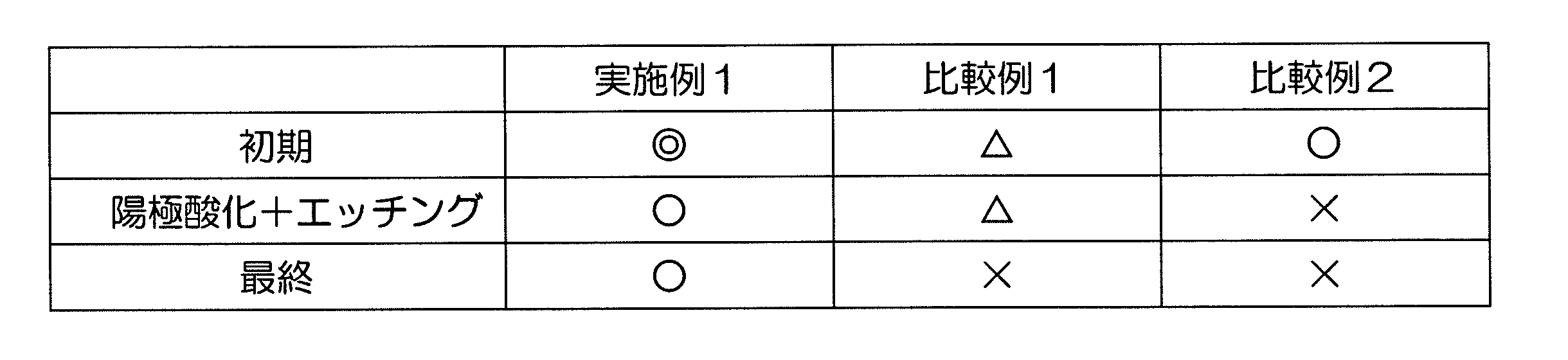
- the adhesion between the glass substrate 12 and the aluminum layer 18 in the obtained mold base material was evaluated as follows by a so-called peel test (cross cut test).
- the SiO 2 is chemically damaged by the treatment liquid entering from the aluminum layer 18 side in the anodizing step and / or etching step. It is thought to be for receiving.
- the treatment liquid enters between the glass substrate 12 and the buffer layer 36 in the anodic oxidation process and / or etching process, It is considered that the alkali metal element in the glass is eluted by the reaction and corrodes the anodized alumina layer.
- Example 2 Comparative Examples 3 and 4
- the glass substrate 12 is used, whereas in Example 2, the plastic film 12 is used.
- the mold substrate of Example 2 has the configuration of the mold substrate 10 shown in FIG. 2, and includes a plastic film 12, an inorganic base layer 14 formed on the surface of the plastic film 12, and an inorganic base layer 14.
- the buffer layer 16 containing aluminum formed in the above and the aluminum layer 18 formed on the surface of the buffer layer 16 are included.
- a conductive layer preferably a valve metal layer
- the material of the conductive layer is preferably a material having a small difference in standard electrode potential from aluminum such as titanium or magnesium so that electric corrosion does not occur. Titanium is also known to have an effect of improving adhesion.
- Example 2 a PET (polyethylene terephthalate) film (manufactured by Kimoto, thickness of 188 ⁇ m) is used as the plastic film 12, a SiO 2 layer having a thickness of 70 nm is formed as the inorganic underlayer 14, and the buffer layer 16 is thick. After forming a single layer of 150 nm thick aluminum oxide (oxygen content 30 at%), an aluminum layer 18 having a thickness of 1 ⁇ m was formed. These series of operations were performed in the same manner as in Example 1.
- the base material of Comparative Example 3 has the configuration of the mold base material 30A shown in FIG. 3A, and in the above-described mold base material manufacturing method, the buffer layer 16 is not formed and the plastic film ( An inorganic underlayer 34 made of SiO 2 was formed on a PET film 12 and then an aluminum layer 18 was formed.
- the base material of Comparative Example 4 has the configuration of the mold base material 30B shown in FIG. 3B.
- the inorganic underlayer 14 is not formed, and the plastic film The same buffer layer 36 as described above was formed on the (PET film) 12 and then the aluminum layer 18 was formed.
- the adhesiveness between the plastic film 12 and the aluminum layer 18 was evaluated by the same method as described above immediately after the aluminum layer 18 was formed and after being immersed in a phosphoric acid aqueous solution (1M, 30 ° C.) for 30 minutes.
- the mold substrate 30A of Comparative Example 3 had an evaluation result of “ ⁇ ” and poor adhesion immediately after film formation and after immersion in a phosphoric acid aqueous solution.
- the mold substrate 30B of Comparative Example 4 had an evaluation result of “ ⁇ ” immediately after film formation, but an evaluation result of “ ⁇ ” after immersion in an aqueous phosphoric acid solution.
- the mold base 10 of Example 2 was evaluated as “ ⁇ ” and good adhesiveness was obtained immediately after film formation and after immersion in an aqueous phosphoric acid solution.
- FIGS. 4 (a) and 4 (b) show SEM images of the surface of the aluminum layer 18 of the mold base 30A of Comparative Example 3 and FIGS. 5 (a) and 5 (b) show the aluminum of the mold base 30B of Comparative Example 4.
- the SEM image of the surface of the layer 18 is shown, and FIGS. 6A and 6B show the SEM images of the surface of the aluminum layer 18 of the mold base 10 of Example 2.
- FIG. 4A to 6A show SEM images immediately after the aluminum layer 18 is formed, and FIG. 4B shows SEM images after immersion in a phosphoric acid aqueous solution.
- the small black dots are pits (dents), and it can be seen from FIG. 4 (b) that they are enlarged by being immersed in the phosphoric acid aqueous solution.
- the mold base 30B of Comparative Example 4 has fewer pits than the mold base 30A of Comparative Example 3, and You can see that it is getting smaller.
- the buffer layer 16 composed of a single aluminum oxide layer was used, but as described in Example 1, the buffer layer 16 composed of a plurality of aluminum oxide layers may be used.
- the plastic film 12 is used.
- the buffer layer 16 an aluminum oxide layer having an oxygen content of 60 at% on the inorganic underlayer 14 side, an aluminum oxide layer having an oxygen content of 1 at% on the aluminum layer 18 side, and asymptotically between these aluminum oxide layers.
- an aluminum oxide layer having a gradient in oxygen content was formed, a good result equal to or better than that of Example 2 was obtained.
- a roll-shaped moth-eye mold can be obtained by fixing the moth-eye mold to the outer peripheral surface of the roll.
- the roll-shaped mold can continuously form a moth-eye structure.
- an aluminum layer can be formed on a plastic substrate other than the illustrated plastic film.
- a moth-eye mold is used as a mold for forming optical elements having a desired concavo-convex shape on the surface, such as a lenticular lens, a brightness enhancement film (for example, BEF manufactured by Sumitomo 3M), a light guide plate, a microlens array, a Fresnel lens, Can be formed to overlap each other.
- a brightness enhancement film for example, BEF manufactured by Sumitomo 3M
- BEF manufactured by Sumitomo 3M
- a light guide plate for example, a microlens array, a Fresnel lens, Can be formed to overlap each other.
- FIGS. 7A to 7C a method for manufacturing a mold for forming a lenticular lens having a moth-eye structure on the surface will be described.
- the lenticular lens has a structure in which a plurality of semi-cylindrical (semi-cylindrical) lenses are arranged in parallel.
- the overall size is 460 mm ⁇ 365 mm
- the pitch (width of the semi-cylindrical lens) is 20 ⁇ m
- the opening angle is 90 ° (the curved surface of the semi-cylindrical lens and the surface perpendicular to the extending direction of the semi-cylindrical lens)
- a curve in which the crosses and corresponds to a quarter of the circumference) is produced.
- a photocurable resin having a concavo-convex structure obtained by inverting the concavo-convex structure of the mold 52 on the plastic film 12a using the mold 52 shown in FIG. 7A.
- a resin layer (for example, an ultraviolet curable resin layer) 12b is formed.
- COP or PET can be used as the plastic film 12a.
- the plastic base material 12A composed of the plastic film 12a and the photocurable resin layer 12b corresponds to the plastic base material 12 shown in FIG.
- an inorganic underlayer (for example, SiO 2 layer) 14 and a buffer layer (for example, an aluminum oxide layer) are formed on the photocurable resin layer 12b having the concavo-convex structure of the plastic substrate 12A.
- a buffer layer for example, an aluminum oxide layer
- a flexible mold 10A can be obtained. If the mold 10A has flexibility, as described above, a roll-shaped mold can be obtained by fixing the mold 10A to the outer peripheral surface of the roll.
- the optical element described above has a periodic uneven structure, but of course, the present invention is not limited to this, and a moth-eye mold can be superimposed on a mold that forms an uneven structure having no periodicity.
- a mold for forming an anti-glare film having antiglare property in which a moth-eye structure is superimposed on a concavo-convex structure exhibiting an antiglare function, is manufactured. You can also
- the mold according to the present invention can be widely used for forming a surface having a moth-eye structure, for example, for forming an antireflection film.
Landscapes
- Engineering & Computer Science (AREA)
- Chemical & Material Sciences (AREA)
- Mechanical Engineering (AREA)
- Physics & Mathematics (AREA)
- Electrochemistry (AREA)
- Materials Engineering (AREA)
- Metallurgy (AREA)
- Organic Chemistry (AREA)
- Chemical Kinetics & Catalysis (AREA)
- Manufacturing & Machinery (AREA)
- General Physics & Mathematics (AREA)
- Optics & Photonics (AREA)
- General Chemical & Material Sciences (AREA)
- Moulds For Moulding Plastics Or The Like (AREA)
- Laminated Bodies (AREA)
- Surface Treatment Of Optical Elements (AREA)
Abstract
Description

図2(a)に示した型基材10の構成を有する実施例1の型基材を以下のようにして作製した。
基板12 :ソーダライムガラス :8.7×10⁻⁶/℃、
無機下地層14 :SiO2 :1.0×10⁻⁶/℃、
緩衝層16 :Al2O3 :6.9×10⁻⁶/℃
アルミニウム層18 :Al :23×10-6/℃
上記の実施例1の型基材では、ガラス基板12を用いたのに対し、本実施例2ではプラスチックフィルム12を用いる。
12 ガラス基板(ガラス基材)またはプラスチックフィルム(プラスチック基材)
14、34 無機下地層
16、36 緩衝層
18、18a アルミニウム層
20 ポーラスアルミナ層
22 細孔
100 モスアイ用型
Claims (7)
- ガラスまたはプラスチックで形成された基材と、
前記基材の表面に形成された無機下地層と、
前記無機下地層の上に形成されたアルミニウムを含有する緩衝層と、
前記緩衝層の表面に形成されたアルミニウム層と、
前記アルミニウム層の表面に形成されたポーラスアルミナ層であって、表面の法線方向から見たときの2次元的な大きさが10nm以上500nm未満の複数の凹部を有する、反転されたモスアイ構造を表面に有するポーラスアルミナ層とを有する、型。 - 前記無機下地層は、酸化シリコン層または酸化チタン層である、請求項1に記載の型。
- 前記緩衝層は、アルミニウムと、酸素または窒素とを含み、前記アルミニウムの含有率が前記無機下地層側よりも前記ポーラスアルミナ層側において高いプロファイルを有する、請求項1または2に記載の型。
- 表面の法線方向から見たときの2次元的な大きさが10nm以上500nm未満の複数の凹部を有する、反転されたモスアイ構造を表面に有する型の製造方法であって、
(a)ガラスまたはプラスチックで形成された基材と、前記基材の表面に形成された無機下地層と、前記無機下地層の上に形成されたアルミニウムを含有する緩衝層と、前記緩衝層の表面に形成されたアルミニウム層とを有する、型基材を用意する工程と、
(b)前記アルミニウム層を部分的に陽極酸化することによって、複数の微細な凹部を有するポーラスアルミナ層を形成する工程と、
(c)前記工程(b)の後に、前記ポーラスアルミナ層を、エッチング液に接触させることによって、前記ポーラスアルミナ層の前記複数の微細な凹部を拡大させる工程と、
(d)前記工程(c)の後に、さらに陽極酸化することによって、前記複数の微細な凹部を成長させる工程と
を包含する、型の製造方法。 - 前記無機下地層は、酸化シリコン層または酸化チタン層である、請求項4に記載の型の製造方法。
- 前記緩衝層は、アルミニウムと、酸素または窒素とを含み、前記アルミニウムの含有率が前記無機下地層側よりも前記アルミニウム層側において高いプロファイルを有する、請求項4または5に記載の型の製造方法。
- 前記工程(d)の後に、前記工程(b)および前記工程(c)をさらに行う、請求項4から6のいずれかに記載の型の製造方法。
Priority Applications (6)
| Application Number | Priority Date | Filing Date | Title |
|---|---|---|---|
| BRPI1010314A BRPI1010314A2 (pt) | 2009-04-09 | 2010-04-06 | molde e metodo de fabricação do mesmo |
| EP10761432.3A EP2418305B1 (en) | 2009-04-09 | 2010-04-06 | Die and method of manufacturing same |
| JP2010542475A JP4648995B2 (ja) | 2009-04-09 | 2010-04-06 | 型およびその製造方法 |
| US13/263,459 US8580135B2 (en) | 2009-04-09 | 2010-04-06 | Die and method of manufacturing same |
| CN201080003284.XA CN102227519B (zh) | 2009-04-09 | 2010-04-06 | 模具及其制造方法 |
| RU2011145304/02A RU2482221C1 (ru) | 2009-04-09 | 2010-04-06 | Форма и способ ее изготовления |
Applications Claiming Priority (2)
| Application Number | Priority Date | Filing Date | Title |
|---|---|---|---|
| JP2009-095267 | 2009-04-09 | ||
| JP2009095267 | 2009-04-09 |
Publications (1)
| Publication Number | Publication Date |
|---|---|
| WO2010116728A1 true WO2010116728A1 (ja) | 2010-10-14 |
Family
ID=42936023
Family Applications (1)
| Application Number | Title | Priority Date | Filing Date |
|---|---|---|---|
| PCT/JP2010/002518 Ceased WO2010116728A1 (ja) | 2009-04-09 | 2010-04-06 | 型およびその製造方法 |
Country Status (7)
| Country | Link |
|---|---|
| US (1) | US8580135B2 (ja) |
| EP (1) | EP2418305B1 (ja) |
| JP (1) | JP4648995B2 (ja) |
| CN (1) | CN102227519B (ja) |
| BR (1) | BRPI1010314A2 (ja) |
| RU (1) | RU2482221C1 (ja) |
| WO (1) | WO2010116728A1 (ja) |
Cited By (10)
| Publication number | Priority date | Publication date | Assignee | Title |
|---|---|---|---|---|
| JP2010131985A (ja) * | 2008-11-07 | 2010-06-17 | Canon Inc | 光学素子成形用金型及び光学素子の成形方法 |
| WO2011135976A1 (ja) | 2010-04-28 | 2011-11-03 | シャープ株式会社 | 型および型の製造方法 |
| WO2012046808A1 (ja) * | 2010-10-08 | 2012-04-12 | シャープ株式会社 | 陽極酸化膜の製造方法 |
| WO2012057073A1 (ja) * | 2010-10-25 | 2012-05-03 | シャープ株式会社 | 太陽熱集熱部材およびその作製方法 |
| WO2012157706A1 (ja) * | 2011-05-17 | 2012-11-22 | キヤノン電子株式会社 | 光学フィルタ、光学機器、電子機器及び反射防止複合体 |
| JP2014129601A (ja) * | 2012-12-29 | 2014-07-10 | Shenzhen Futaihong Precision Industrial Co Ltd | ステンレス鋼の表面処理方法及びその方法によって製造されたハウジング |
| KR20150010789A (ko) | 2012-06-06 | 2015-01-28 | 샤프 가부시키가이샤 | 형 기재, 형 기재의 제조 방법, 형의 제조 방법 및 형 |
| US9108351B2 (en) | 2010-03-09 | 2015-08-18 | Sharp Kabushiki Kaisha | Method for forming anodized layer, method for producing mold and method for producing antireflective film |
| US9512535B2 (en) | 2011-04-01 | 2016-12-06 | Sharp Kabushiki Kaisha | Mold production method |
| US9556532B2 (en) | 2010-03-31 | 2017-01-31 | Sharp Kabushiki Kaisha | Die, process for producing die, and process for producing antireflection film |
Families Citing this family (3)
| Publication number | Priority date | Publication date | Assignee | Title |
|---|---|---|---|---|
| WO2010125795A1 (ja) | 2009-04-30 | 2010-11-04 | シャープ株式会社 | 型およびその製造方法 |
| KR20120088920A (ko) * | 2011-02-01 | 2012-08-09 | 삼성전기주식회사 | 터치패널 |
| CN102517620B (zh) * | 2011-12-06 | 2014-12-17 | 中国科学院宁波材料技术与工程研究所 | 一种渐变折射率减反射膜的制备方法 |
Citations (7)
| Publication number | Priority date | Publication date | Assignee | Title |
|---|---|---|---|---|
| JP2001517319A (ja) | 1997-03-04 | 2001-10-02 | フラウンホファー.ゲゼルシャフト.ツール.フォルデンウング.デール.アンゲヴァンドテン.フォルシュング.エー.ファウ. | 反射防止膜とその製法 |
| JP2003531962A (ja) | 2000-04-28 | 2003-10-28 | アルコーブ サーフィシーズ ゲーエムベーハー | 型押し具、これを製造する方法、加工物の表面を構築する方法、及び陽極酸化表面層の使用 |
| JP2005156695A (ja) | 2003-11-21 | 2005-06-16 | Kanagawa Acad Of Sci & Technol | 反射防止膜及びその製造方法、並びに反射防止膜作製用スタンパ及びその製造方法 |
| JP2006028604A (ja) * | 2004-07-16 | 2006-02-02 | Ricoh Co Ltd | 微細形状転写方法、鋳型製作方法、鋳型表面処理法及び鋳型 |
| WO2006059686A1 (ja) | 2004-12-03 | 2006-06-08 | Sharp Kabushiki Kaisha | 反射防止材、光学素子、および表示装置ならびにスタンパの製造方法およびスタンパを用いた反射防止材の製造方法 |
| JP2008075175A (ja) * | 2006-08-24 | 2008-04-03 | Canon Inc | 構造体の製造方法 |
| JP2010090430A (ja) * | 2008-10-07 | 2010-04-22 | Fuji Electric Device Technology Co Ltd | アルミニウム合金形成基板及びその製造方法 |
Family Cites Families (12)
| Publication number | Priority date | Publication date | Assignee | Title |
|---|---|---|---|---|
| US4193848A (en) * | 1973-08-13 | 1980-03-18 | Swiss Aluminium Ltd. | Process for the production of composite material |
| JP3436983B2 (ja) * | 1994-09-02 | 2003-08-18 | 富士通株式会社 | モールド成形品の分離方法 |
| JP2955704B2 (ja) * | 1995-07-25 | 1999-10-04 | 株式会社有沢製作所 | 航空機用の液晶プロジェクター用反射型スクリーン及び液晶プロジェクター用反射型スクリーンの製造方法 |
| JP3440754B2 (ja) * | 1997-05-19 | 2003-08-25 | 信越化学工業株式会社 | 室温硬化性オルガノポリシロキサン組成物 |
| US6140701A (en) * | 1999-08-31 | 2000-10-31 | Micron Technology, Inc. | Suppression of hillock formation in thin aluminum films |
| US7066234B2 (en) * | 2001-04-25 | 2006-06-27 | Alcove Surfaces Gmbh | Stamping tool, casting mold and methods for structuring a surface of a work piece |
| RU2186159C1 (ru) * | 2001-01-19 | 2002-07-27 | Государственное предприятие "Всероссийский научно-исследовательский институт авиационных материалов" | Способ нанесения покрытия на деталь из алюминия и алюминиевых сплавов |
| JP2005008909A (ja) * | 2003-06-16 | 2005-01-13 | Canon Inc | 構造体の製造方法 |
| JP2006059686A (ja) | 2004-08-20 | 2006-03-02 | Yazaki Corp | 平型ケーブル |
| CN101566699B (zh) * | 2004-12-03 | 2015-12-16 | 夏普株式会社 | 抗反射材料、光学元件、显示器件及压模的制造方法和使用了压模的抗反射材料的制造方法 |
| US7713768B2 (en) * | 2006-06-14 | 2010-05-11 | Kanagawa Academy Of Science And Technology | Anti-reflective film and production method thereof, and stamper for producing anti-reflective film and production method thereof |
| US7655127B2 (en) * | 2006-11-27 | 2010-02-02 | 3M Innovative Properties Company | Method of fabricating thin film transistor |
-
2010
- 2010-04-06 RU RU2011145304/02A patent/RU2482221C1/ru active
- 2010-04-06 BR BRPI1010314A patent/BRPI1010314A2/pt not_active IP Right Cessation
- 2010-04-06 CN CN201080003284.XA patent/CN102227519B/zh not_active Expired - Fee Related
- 2010-04-06 US US13/263,459 patent/US8580135B2/en not_active Expired - Fee Related
- 2010-04-06 WO PCT/JP2010/002518 patent/WO2010116728A1/ja not_active Ceased
- 2010-04-06 EP EP10761432.3A patent/EP2418305B1/en not_active Not-in-force
- 2010-04-06 JP JP2010542475A patent/JP4648995B2/ja not_active Expired - Fee Related
Patent Citations (7)
| Publication number | Priority date | Publication date | Assignee | Title |
|---|---|---|---|---|
| JP2001517319A (ja) | 1997-03-04 | 2001-10-02 | フラウンホファー.ゲゼルシャフト.ツール.フォルデンウング.デール.アンゲヴァンドテン.フォルシュング.エー.ファウ. | 反射防止膜とその製法 |
| JP2003531962A (ja) | 2000-04-28 | 2003-10-28 | アルコーブ サーフィシーズ ゲーエムベーハー | 型押し具、これを製造する方法、加工物の表面を構築する方法、及び陽極酸化表面層の使用 |
| JP2005156695A (ja) | 2003-11-21 | 2005-06-16 | Kanagawa Acad Of Sci & Technol | 反射防止膜及びその製造方法、並びに反射防止膜作製用スタンパ及びその製造方法 |
| JP2006028604A (ja) * | 2004-07-16 | 2006-02-02 | Ricoh Co Ltd | 微細形状転写方法、鋳型製作方法、鋳型表面処理法及び鋳型 |
| WO2006059686A1 (ja) | 2004-12-03 | 2006-06-08 | Sharp Kabushiki Kaisha | 反射防止材、光学素子、および表示装置ならびにスタンパの製造方法およびスタンパを用いた反射防止材の製造方法 |
| JP2008075175A (ja) * | 2006-08-24 | 2008-04-03 | Canon Inc | 構造体の製造方法 |
| JP2010090430A (ja) * | 2008-10-07 | 2010-04-22 | Fuji Electric Device Technology Co Ltd | アルミニウム合金形成基板及びその製造方法 |
Non-Patent Citations (1)
| Title |
|---|
| See also references of EP2418305A4 |
Cited By (17)
| Publication number | Priority date | Publication date | Assignee | Title |
|---|---|---|---|---|
| JP2010131985A (ja) * | 2008-11-07 | 2010-06-17 | Canon Inc | 光学素子成形用金型及び光学素子の成形方法 |
| US9108351B2 (en) | 2010-03-09 | 2015-08-18 | Sharp Kabushiki Kaisha | Method for forming anodized layer, method for producing mold and method for producing antireflective film |
| US9556532B2 (en) | 2010-03-31 | 2017-01-31 | Sharp Kabushiki Kaisha | Die, process for producing die, and process for producing antireflection film |
| US9405043B2 (en) | 2010-04-28 | 2016-08-02 | Sharp Kabushiki Kaisha | Mold and process for production of mold |
| JP5027347B2 (ja) * | 2010-04-28 | 2012-09-19 | シャープ株式会社 | 型および型の製造方法 |
| WO2011135976A1 (ja) | 2010-04-28 | 2011-11-03 | シャープ株式会社 | 型および型の製造方法 |
| US9133558B2 (en) | 2010-10-08 | 2015-09-15 | Sharp Kabushiki Kaisha | Method for producing anodized film |
| JP5595511B2 (ja) * | 2010-10-08 | 2014-09-24 | シャープ株式会社 | 陽極酸化膜の製造方法 |
| WO2012046808A1 (ja) * | 2010-10-08 | 2012-04-12 | シャープ株式会社 | 陽極酸化膜の製造方法 |
| WO2012057073A1 (ja) * | 2010-10-25 | 2012-05-03 | シャープ株式会社 | 太陽熱集熱部材およびその作製方法 |
| US9512535B2 (en) | 2011-04-01 | 2016-12-06 | Sharp Kabushiki Kaisha | Mold production method |
| US9316766B2 (en) | 2011-05-17 | 2016-04-19 | Canon Denshi Kabushiki Kaisha | Optical filter, optical device, electronic device and anti-reflection composite |
| JP6006718B2 (ja) * | 2011-05-17 | 2016-10-12 | キヤノン電子株式会社 | 光学フィルタ、光学機器、電子機器及び反射防止複合体 |
| WO2012157706A1 (ja) * | 2011-05-17 | 2012-11-22 | キヤノン電子株式会社 | 光学フィルタ、光学機器、電子機器及び反射防止複合体 |
| KR20150010789A (ko) | 2012-06-06 | 2015-01-28 | 샤프 가부시키가이샤 | 형 기재, 형 기재의 제조 방법, 형의 제조 방법 및 형 |
| US9914243B2 (en) | 2012-06-06 | 2018-03-13 | Sharp Kabushiki Kaisha | Mold base material, production method for mold base material, mold production method, and mold |
| JP2014129601A (ja) * | 2012-12-29 | 2014-07-10 | Shenzhen Futaihong Precision Industrial Co Ltd | ステンレス鋼の表面処理方法及びその方法によって製造されたハウジング |
Also Published As
| Publication number | Publication date |
|---|---|
| JP4648995B2 (ja) | 2011-03-09 |
| CN102227519A (zh) | 2011-10-26 |
| EP2418305A4 (en) | 2013-01-02 |
| JPWO2010116728A1 (ja) | 2012-10-18 |
| EP2418305A1 (en) | 2012-02-15 |
| CN102227519B (zh) | 2014-07-02 |
| US20120018613A1 (en) | 2012-01-26 |
| RU2482221C1 (ru) | 2013-05-20 |
| EP2418305B1 (en) | 2016-09-28 |
| US8580135B2 (en) | 2013-11-12 |
| BRPI1010314A2 (pt) | 2016-03-15 |
Similar Documents
| Publication | Publication Date | Title |
|---|---|---|
| JP4648995B2 (ja) | 型およびその製造方法 | |
| JP4677515B2 (ja) | 型およびその製造方法 | |
| JP5027347B2 (ja) | 型および型の製造方法 | |
| CN102803577B (zh) | 模具和模具的制造方法以及防反射膜的制造方法 | |
| US9366785B2 (en) | Mold, method for manufacturing a mold, and antireflective film | |
| JP5615971B2 (ja) | 型の製造方法 | |
| JP5102324B2 (ja) | 型の製造方法および型を用いた反射防止膜の製造方法 | |
| JP5595511B2 (ja) | 陽極酸化膜の製造方法 | |
| JP6458051B2 (ja) | 型および型の製造方法ならびに反射防止膜 | |
| JP5833763B2 (ja) | 型の製造方法 |
Legal Events
| Date | Code | Title | Description |
|---|---|---|---|
| WWE | Wipo information: entry into national phase |
Ref document number: 201080003284.X Country of ref document: CN |
|
| WWE | Wipo information: entry into national phase |
Ref document number: 2010542475 Country of ref document: JP |
|
| 121 | Ep: the epo has been informed by wipo that ep was designated in this application |
Ref document number: 10761432 Country of ref document: EP Kind code of ref document: A1 |
|
| WWE | Wipo information: entry into national phase |
Ref document number: 13263459 Country of ref document: US |
|
| NENP | Non-entry into the national phase |
Ref country code: DE |
|
| REEP | Request for entry into the european phase |
Ref document number: 2010761432 Country of ref document: EP |
|
| WWE | Wipo information: entry into national phase |
Ref document number: 2010761432 Country of ref document: EP |
|
| WWE | Wipo information: entry into national phase |
Ref document number: 2338/MUMNP/2011 Country of ref document: IN |
|
| ENP | Entry into the national phase |
Ref document number: 2011145304 Country of ref document: RU Kind code of ref document: A |
|
| REG | Reference to national code |
Ref country code: BR Ref legal event code: B01A Ref document number: PI1010314 Country of ref document: BR |
|
| ENP | Entry into the national phase |
Ref document number: PI1010314 Country of ref document: BR Kind code of ref document: A2 Effective date: 20111004 |