WO2010109964A1 - 半導体集積回路装置 - Google Patents
半導体集積回路装置 Download PDFInfo
- Publication number
- WO2010109964A1 WO2010109964A1 PCT/JP2010/051916 JP2010051916W WO2010109964A1 WO 2010109964 A1 WO2010109964 A1 WO 2010109964A1 JP 2010051916 W JP2010051916 W JP 2010051916W WO 2010109964 A1 WO2010109964 A1 WO 2010109964A1
- Authority
- WO
- WIPO (PCT)
- Prior art keywords
- motor
- resolver
- cpu
- value
- semiconductor integrated
- Prior art date
- Legal status (The legal status is an assumption and is not a legal conclusion. Google has not performed a legal analysis and makes no representation as to the accuracy of the status listed.)
- Ceased
Links
Images






Classifications
-
- B—PERFORMING OPERATIONS; TRANSPORTING
- B60—VEHICLES IN GENERAL
- B60L—PROPULSION OF ELECTRICALLY-PROPELLED VEHICLES; SUPPLYING ELECTRIC POWER FOR AUXILIARY EQUIPMENT OF ELECTRICALLY-PROPELLED VEHICLES; ELECTRODYNAMIC BRAKE SYSTEMS FOR VEHICLES IN GENERAL; MAGNETIC SUSPENSION OR LEVITATION FOR VEHICLES; MONITORING OPERATING VARIABLES OF ELECTRICALLY-PROPELLED VEHICLES; ELECTRIC SAFETY DEVICES FOR ELECTRICALLY-PROPELLED VEHICLES
- B60L15/00—Methods, circuits, or devices for controlling the traction-motor speed of electrically-propelled vehicles
- B60L15/20—Methods, circuits, or devices for controlling the traction-motor speed of electrically-propelled vehicles for control of the vehicle or its driving motor to achieve a desired performance, e.g. speed, torque, programmed variation of speed
-
- H—ELECTRICITY
- H02—GENERATION; CONVERSION OR DISTRIBUTION OF ELECTRIC POWER
- H02P—CONTROL OR REGULATION OF ELECTRIC MOTORS, ELECTRIC GENERATORS OR DYNAMO-ELECTRIC CONVERTERS; CONTROLLING TRANSFORMERS, REACTORS OR CHOKE COILS
- H02P21/00—Arrangements or methods for the control of electric machines by vector control, e.g. by control of field orientation
-
- B—PERFORMING OPERATIONS; TRANSPORTING
- B60—VEHICLES IN GENERAL
- B60L—PROPULSION OF ELECTRICALLY-PROPELLED VEHICLES; SUPPLYING ELECTRIC POWER FOR AUXILIARY EQUIPMENT OF ELECTRICALLY-PROPELLED VEHICLES; ELECTRODYNAMIC BRAKE SYSTEMS FOR VEHICLES IN GENERAL; MAGNETIC SUSPENSION OR LEVITATION FOR VEHICLES; MONITORING OPERATING VARIABLES OF ELECTRICALLY-PROPELLED VEHICLES; ELECTRIC SAFETY DEVICES FOR ELECTRICALLY-PROPELLED VEHICLES
- B60L15/00—Methods, circuits, or devices for controlling the traction-motor speed of electrically-propelled vehicles
- B60L15/02—Methods, circuits, or devices for controlling the traction-motor speed of electrically-propelled vehicles characterised by the form of the current used in the control circuit
- B60L15/025—Methods, circuits, or devices for controlling the traction-motor speed of electrically-propelled vehicles characterised by the form of the current used in the control circuit using field orientation; Vector control; Direct Torque Control [DTC]
-
- B—PERFORMING OPERATIONS; TRANSPORTING
- B60—VEHICLES IN GENERAL
- B60L—PROPULSION OF ELECTRICALLY-PROPELLED VEHICLES; SUPPLYING ELECTRIC POWER FOR AUXILIARY EQUIPMENT OF ELECTRICALLY-PROPELLED VEHICLES; ELECTRODYNAMIC BRAKE SYSTEMS FOR VEHICLES IN GENERAL; MAGNETIC SUSPENSION OR LEVITATION FOR VEHICLES; MONITORING OPERATING VARIABLES OF ELECTRICALLY-PROPELLED VEHICLES; ELECTRIC SAFETY DEVICES FOR ELECTRICALLY-PROPELLED VEHICLES
- B60L15/00—Methods, circuits, or devices for controlling the traction-motor speed of electrically-propelled vehicles
- B60L15/20—Methods, circuits, or devices for controlling the traction-motor speed of electrically-propelled vehicles for control of the vehicle or its driving motor to achieve a desired performance, e.g. speed, torque, programmed variation of speed
- B60L15/2045—Methods, circuits, or devices for controlling the traction-motor speed of electrically-propelled vehicles for control of the vehicle or its driving motor to achieve a desired performance, e.g. speed, torque, programmed variation of speed for optimising the use of energy
-
- B—PERFORMING OPERATIONS; TRANSPORTING
- B60—VEHICLES IN GENERAL
- B60W—CONJOINT CONTROL OF VEHICLE SUB-UNITS OF DIFFERENT TYPE OR DIFFERENT FUNCTION; CONTROL SYSTEMS SPECIALLY ADAPTED FOR HYBRID VEHICLES; ROAD VEHICLE DRIVE CONTROL SYSTEMS FOR PURPOSES NOT RELATED TO THE CONTROL OF A PARTICULAR SUB-UNIT
- B60W10/00—Conjoint control of vehicle sub-units of different type or different function
-
- G—PHYSICS
- G01—MEASURING; TESTING
- G01D—MEASURING NOT SPECIALLY ADAPTED FOR A SPECIFIC VARIABLE; ARRANGEMENTS FOR MEASURING TWO OR MORE VARIABLES NOT COVERED IN A SINGLE OTHER SUBCLASS; TARIFF METERING APPARATUS; MEASURING OR TESTING NOT OTHERWISE PROVIDED FOR
- G01D5/00—Mechanical means for transferring the output of a sensing member; Means for converting the output of a sensing member to another variable where the form or nature of the sensing member does not constrain the means for converting; Transducers not specially adapted for a specific variable
- G01D5/12—Mechanical means for transferring the output of a sensing member; Means for converting the output of a sensing member to another variable where the form or nature of the sensing member does not constrain the means for converting; Transducers not specially adapted for a specific variable using electric or magnetic means
- G01D5/244—Mechanical means for transferring the output of a sensing member; Means for converting the output of a sensing member to another variable where the form or nature of the sensing member does not constrain the means for converting; Transducers not specially adapted for a specific variable using electric or magnetic means influencing characteristics of pulses or pulse trains; generating pulses or pulse trains
- G01D5/245—Mechanical means for transferring the output of a sensing member; Means for converting the output of a sensing member to another variable where the form or nature of the sensing member does not constrain the means for converting; Transducers not specially adapted for a specific variable using electric or magnetic means influencing characteristics of pulses or pulse trains; generating pulses or pulse trains using a variable number of pulses in a train
-
- H—ELECTRICITY
- H02—GENERATION; CONVERSION OR DISTRIBUTION OF ELECTRIC POWER
- H02P—CONTROL OR REGULATION OF ELECTRIC MOTORS, ELECTRIC GENERATORS OR DYNAMO-ELECTRIC CONVERTERS; CONTROLLING TRANSFORMERS, REACTORS OR CHOKE COILS
- H02P23/00—Arrangements or methods for the control of AC motors characterised by a control method other than vector control
- H02P23/0004—Control strategies in general, e.g. linear type, e.g. P, PI, PID, using robust control
- H02P23/0027—Control strategies in general, e.g. linear type, e.g. P, PI, PID, using robust control using different modes of control depending on a parameter, e.g. the speed
-
- H—ELECTRICITY
- H02—GENERATION; CONVERSION OR DISTRIBUTION OF ELECTRIC POWER
- H02P—CONTROL OR REGULATION OF ELECTRIC MOTORS, ELECTRIC GENERATORS OR DYNAMO-ELECTRIC CONVERTERS; CONTROLLING TRANSFORMERS, REACTORS OR CHOKE COILS
- H02P27/00—Arrangements or methods for the control of AC motors characterised by the kind of supply voltage
- H02P27/04—Arrangements or methods for the control of AC motors characterised by the kind of supply voltage using variable-frequency supply voltage, e.g. inverter or converter supply voltage
-
- H—ELECTRICITY
- H02—GENERATION; CONVERSION OR DISTRIBUTION OF ELECTRIC POWER
- H02P—CONTROL OR REGULATION OF ELECTRIC MOTORS, ELECTRIC GENERATORS OR DYNAMO-ELECTRIC CONVERTERS; CONTROLLING TRANSFORMERS, REACTORS OR CHOKE COILS
- H02P6/00—Arrangements for controlling synchronous motors or other dynamo-electric motors using electronic commutation dependent on the rotor position; Electronic commutators therefor
- H02P6/14—Electronic commutators
- H02P6/16—Circuit arrangements for detecting position
- H02P6/18—Circuit arrangements for detecting position without separate position detecting elements
- H02P6/181—Circuit arrangements for detecting position without separate position detecting elements using different methods depending on the speed
-
- H—ELECTRICITY
- H02—GENERATION; CONVERSION OR DISTRIBUTION OF ELECTRIC POWER
- H02P—CONTROL OR REGULATION OF ELECTRIC MOTORS, ELECTRIC GENERATORS OR DYNAMO-ELECTRIC CONVERTERS; CONTROLLING TRANSFORMERS, REACTORS OR CHOKE COILS
- H02P7/00—Arrangements for regulating or controlling the speed or torque of electric DC motors
- H02P7/06—Arrangements for regulating or controlling the speed or torque of electric DC motors for regulating or controlling an individual DC dynamo-electric motor by varying field or armature current
-
- B—PERFORMING OPERATIONS; TRANSPORTING
- B60—VEHICLES IN GENERAL
- B60L—PROPULSION OF ELECTRICALLY-PROPELLED VEHICLES; SUPPLYING ELECTRIC POWER FOR AUXILIARY EQUIPMENT OF ELECTRICALLY-PROPELLED VEHICLES; ELECTRODYNAMIC BRAKE SYSTEMS FOR VEHICLES IN GENERAL; MAGNETIC SUSPENSION OR LEVITATION FOR VEHICLES; MONITORING OPERATING VARIABLES OF ELECTRICALLY-PROPELLED VEHICLES; ELECTRIC SAFETY DEVICES FOR ELECTRICALLY-PROPELLED VEHICLES
- B60L2240/00—Control parameters of input or output; Target parameters
- B60L2240/40—Drive Train control parameters
- B60L2240/42—Drive Train control parameters related to electric machines
- B60L2240/421—Speed
-
- B—PERFORMING OPERATIONS; TRANSPORTING
- B60—VEHICLES IN GENERAL
- B60L—PROPULSION OF ELECTRICALLY-PROPELLED VEHICLES; SUPPLYING ELECTRIC POWER FOR AUXILIARY EQUIPMENT OF ELECTRICALLY-PROPELLED VEHICLES; ELECTRODYNAMIC BRAKE SYSTEMS FOR VEHICLES IN GENERAL; MAGNETIC SUSPENSION OR LEVITATION FOR VEHICLES; MONITORING OPERATING VARIABLES OF ELECTRICALLY-PROPELLED VEHICLES; ELECTRIC SAFETY DEVICES FOR ELECTRICALLY-PROPELLED VEHICLES
- B60L2240/00—Control parameters of input or output; Target parameters
- B60L2240/40—Drive Train control parameters
- B60L2240/42—Drive Train control parameters related to electric machines
- B60L2240/429—Current
-
- Y—GENERAL TAGGING OF NEW TECHNOLOGICAL DEVELOPMENTS; GENERAL TAGGING OF CROSS-SECTIONAL TECHNOLOGIES SPANNING OVER SEVERAL SECTIONS OF THE IPC; TECHNICAL SUBJECTS COVERED BY FORMER USPC CROSS-REFERENCE ART COLLECTIONS [XRACs] AND DIGESTS
- Y02—TECHNOLOGIES OR APPLICATIONS FOR MITIGATION OR ADAPTATION AGAINST CLIMATE CHANGE
- Y02T—CLIMATE CHANGE MITIGATION TECHNOLOGIES RELATED TO TRANSPORTATION
- Y02T10/00—Road transport of goods or passengers
- Y02T10/60—Other road transportation technologies with climate change mitigation effect
- Y02T10/64—Electric machine technologies in electromobility
-
- Y—GENERAL TAGGING OF NEW TECHNOLOGICAL DEVELOPMENTS; GENERAL TAGGING OF CROSS-SECTIONAL TECHNOLOGIES SPANNING OVER SEVERAL SECTIONS OF THE IPC; TECHNICAL SUBJECTS COVERED BY FORMER USPC CROSS-REFERENCE ART COLLECTIONS [XRACs] AND DIGESTS
- Y02—TECHNOLOGIES OR APPLICATIONS FOR MITIGATION OR ADAPTATION AGAINST CLIMATE CHANGE
- Y02T—CLIMATE CHANGE MITIGATION TECHNOLOGIES RELATED TO TRANSPORTATION
- Y02T10/00—Road transport of goods or passengers
- Y02T10/60—Other road transportation technologies with climate change mitigation effect
- Y02T10/72—Electric energy management in electromobility
-
- Y—GENERAL TAGGING OF NEW TECHNOLOGICAL DEVELOPMENTS; GENERAL TAGGING OF CROSS-SECTIONAL TECHNOLOGIES SPANNING OVER SEVERAL SECTIONS OF THE IPC; TECHNICAL SUBJECTS COVERED BY FORMER USPC CROSS-REFERENCE ART COLLECTIONS [XRACs] AND DIGESTS
- Y10—TECHNICAL SUBJECTS COVERED BY FORMER USPC
- Y10S—TECHNICAL SUBJECTS COVERED BY FORMER USPC CROSS-REFERENCE ART COLLECTIONS [XRACs] AND DIGESTS
- Y10S903/00—Hybrid electric vehicles, HEVS
- Y10S903/902—Prime movers comprising electrical and internal combustion motors
- Y10S903/903—Prime movers comprising electrical and internal combustion motors having energy storing means, e.g. battery, capacitor
Definitions
- the present invention relates to a semiconductor integrated circuit device, and more particularly to an efficient motor control technique.
- This technology can be suitably used for a motor control controller used in an electric vehicle, a hybrid vehicle, or the like.
- An electric vehicle or a hybrid vehicle is provided with a drive motor.
- a technique for detecting the rotation angle of the rotor (output shaft) of this drive motor for example, a technique using a resolver is known.
- Position detection by this type of resolver is performed, for example, by converting the output of the resolver into a rotation angle by an R / D (Resolver / Digital) converter, and the motor control device controls the rotation of the drive motor in accordance with the rotation angle. Is controlled (see, for example, Patent Document 1).
- the rotation angle of the motor is detected by a resolver, the rotation angle information is converted by the R / D processing unit, and then the output value of the resolver is corrected by the correction unit. It is described that control is performed, and that correction value information for correcting the output value of the resolver is stored in the PROM.
- the inventor has studied the motor control device having the configuration described in Patent Document 1, and has recognized that the following problems that are not described in Patent Document 1 exist.
- the engine speed is reduced by gears in order to prevent the engine speed from becoming too high in consideration of fuel combustion efficiency.
- By enabling the rotation it is possible to relatively reduce the reduction of the rotation speed depending on the gear.
- the practical rotational speed of the motor in the hybrid vehicle as well as in the electric vehicle it is desirable to control from 0 rpm in the stopped state to a high rotational speed exceeding 10,000 rpm, and high rotation is expected.
- the motor control device needs to control the current supplied to the stator coil / rotor coil of the motor.
- the CPU receives an interrupt notification and the correction unit It can be estimated that a program for driving the motor driver is executed according to the correction value.
- the interrupt notification frequency is 12 KHz (10000 rpm (about 166 rps) ⁇ 360/5) when the motor is driven at 10000 rpm.
- the CPU operating frequency (assuming 1 step / 1 clock cycle) ) Requires 48 MHz (12K ⁇ 4000 steps). On the other hand, it becomes 36 MHz in the stop state.
- An object of the present invention is to provide a semiconductor integrated circuit device for motor control in which the operating frequency of a CPU is suppressed.
- Another object of the present invention is to provide a semiconductor integrated circuit device for motor control that can reduce power consumption.
- Another object of the present invention is to provide a semiconductor integrated circuit device for a motor driver capable of smoothly and efficiently controlling the motor from a stopped state of the motor to a high speed rotation.
- the semiconductor integrated circuit device determines the rotational speed of the motor, and changes the operation according to the rotational speed of the motor.
- the semiconductor integrated circuit device determines the rotational speed of the motor, and when the rotational speed of the motor is smaller than a predetermined rotational speed, the motor drive control is performed by CPU software processing, and the rotational speed of the motor is When larger, motor drive control is performed by a hardware circuit.
- the semiconductor integrated circuit device determines the rotational speed of the motor, and performs control so as to change the motor driving waveform when the rotational speed of the motor is smaller than or larger than the predetermined rotational speed. is there.
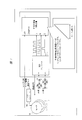
- FIG. 1 is a block diagram illustrating a configuration example of a motor drive system used in an electric vehicle, a hybrid vehicle, and the like according to Embodiment 1 of the present invention.
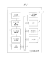
- FIG. 2 is a block diagram illustrating a configuration example of a semiconductor integrated circuit device used in the motor drive system of FIG. 1. It is explanatory drawing which shows the drive waveform output example in the motor of FIG.
- FIG. 3 is an operation explanatory diagram of motor control by the semiconductor integrated circuit device of FIG. 2.
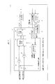
- FIG. 3 is an explanatory diagram showing a configuration example of a motor control arithmetic circuit provided in the semiconductor integrated circuit device of FIG. 2. It is an image figure of the resolver value containing an error, and an ideal resolver value.
- FIG. 3 is an explanatory diagram showing an outline of operation of a resolver value correction technique by the semiconductor integrated circuit device of FIG. 2. It is explanatory drawing which showed the difference of the motor maximum rotation speed of the correction process of software, and a hardware process. It is explanatory drawing which shows the comparative example of the consumption current at the time of correct
- FIG. 3 is an explanatory diagram showing an outline of operation of a resolver value correction technique by the semiconductor integrated circuit device of FIG. 2. It is explanatory drawing which showed the difference of the motor maximum rotation speed of the correction process of software, and a hardware process. It is explanatory drawing which shows the comparative example of the consumption current at the time of correct
- FIG. 3 is an explanatory diagram showing an example of a technique for correcting a resolver value by a resolver value correction arithmetic circuit provided in the semiconductor integrated circuit device of FIG. 2. It is explanatory drawing which shows the comparative example at the time of switching the energization phase of a motor by the compare match with the resolver value containing an error, and the compare match with the resolver value by which error correction
- FIG. 15 is an explanatory diagram illustrating an example of operation timing in the CPU by the semiconductor integrated circuit of FIG. 14. It is a block diagram which shows the structural example of the semiconductor integrated circuit device as another aspect of Embodiment 2 of this invention. It is explanatory drawing which shows the example of operation timing in CPU by the semiconductor integrated circuit of FIG.
- the semiconductor integrated circuit device (1) determines whether the motor is rotating at medium to high speed, or whether it is stopped to rotate at a low speed.
- the motor drive control is performed by software processing of 10), and when the motor is rotating at a medium to high speed, a motor rotation speed determination circuit (a control for switching to perform the motor drive control by the hardware circuit (5, 6)) ( 9).
- the semiconductor integrated circuit device (1) includes an error obtained by counting up the resolver signal output from the resolver attached to the motor converted into a digital signal as a hardware circuit that performs motor drive control.
- a resolver value correction calculation unit (5, 12) for sequentially correcting the resolver value by hardware processing is provided.
- the resolver value correction calculation unit (5, 12) includes a resolver value including an error in one resolver period and a reference resolver value including no error.
- the resolver value correction arithmetic circuit (5) adds / subtracts the first error correction data to / from the resolver value including the input error, and makes an arbitrary period obtained by dividing one period of the resolver into two or more.
- the difference between the resolver value including no error and the resolver value including the error is calculated as second error correction data, and the ratio between the second error correction data and the first error correction data is compared.
- Third error A positive data, and performs the processing for reflecting the next resolver values.
- the semiconductor integrated circuit device (1) has a hardware configuration in which the resolver value correction arithmetic circuit performs a data flow operation.
- the semiconductor integrated circuit device (1) includes, as another hardware circuit that performs motor drive control, a motor control unit (6, 6) that generates a motor drive waveform that generates a drive control signal that drives the motor. 7), and the motor control unit (6, 7) calculates the position data of the motor from the resolver value corrected by the resolver value correction calculation unit (5, 12), and the position data and the motor current value flowing through the motor
- the current command value is calculated from the motor current command value, and the motor drive waveform is generated from the current command value.
- the motor drive system includes a motor (M), a resolver (2), a power module (PM), and a semiconductor integrated circuit device (1).
- the semiconductor integrated circuit device (1) includes an R / D converter (3), an R / D conversion interface (4), a motor waveform output circuit (7), and an A / D converter (8). .
- the resolver (2) is connected to the R / D converter (3), and the output of the R / D converter (3) is connected to the R / D conversion interface (4).
- the current of the motor (M) is input to the A / D converter (8).
- a motor drive waveform is output from the motor waveform output circuit (7), and the motor (M) is driven via the power module (PM).
- FIG. 1 is a block diagram illustrating a configuration example of a motor drive system used in an electric vehicle or a hybrid vehicle (hereinafter referred to as an electric vehicle).
- the semiconductor integrated circuit device 1 is, for example, a microcomputer (also referred to as a microcontroller) that controls, for example, a three-phase motor M used in an electric vehicle. is there.
- a resolver 2 that detects the rotation angle of the motor M is incorporated in the motor M.
- An R / D converter 3 is connected to the resolver 2, and a semiconductor integrated circuit device 1 is connected to the R / D converter 3.
- the R / D converter 3 is provided outside the semiconductor integrated circuit device 1 here, the R / D converter 3 may be provided inside the semiconductor integrated circuit device 1.
- the number of parts of the motor drive system can be reduced, the system can be downsized, and the cost can be reduced.
- the resolver 2 generates a sine wave and a cosine wave based on the excitation signal output from the R / D converter 3.
- the R / D converter 3 converts the sine wave and cosine wave of the analog signal generated by the resolver 2 into a digital signal and outputs the digital signal to the semiconductor integrated circuit device 1.
- the R / D converter 3 outputs a sine wave of an analog signal, a digital signal A converted from a cosine wave to a digital signal, a digital signal B, and a Z-phase signal Z generated once for each cycle of the motor M.
- the semiconductor integrated circuit device 1 counts up the digital signals A and B converted by the R / D converter 3, detects the rotation angle (for example, 0 ° to 360 °) of the motor M, and responds to the rotation angle of the motor M.
- a motor drive waveform is generated from the current command value generated in this way and output to the power module PM that drives the motor M.
- the Z-phase signal Z is input, the count-up is cleared.
- FIG. 2 is a block diagram showing a configuration example of the semiconductor integrated circuit device 1.
- the semiconductor integrated circuit device 1 includes an R / D conversion interface 4, a resolver value correction arithmetic circuit 5, a motor control arithmetic circuit 6 serving as a motor control unit, a motor waveform output circuit 7 also serving as a motor control unit, an A / D (Analog / Digital) converter 8, motor rotation speed determination circuit 9, CPU (Central Processing Unit) 10, interrupt controller 11, and memory unit 12 serving as a data storage unit. Further, the resolver value correction calculation circuit 5 and the memory unit 12 constitute a resolver value correction calculation unit.
- the A / D converter 8, the motor rotation speed determination circuit 9, the CPU 10, the interrupt controller 11, and the memory unit 12 are connected to each other via a bus 13, and the resolver value correction arithmetic circuit is a memory unit 12 is connected to the memory unit 12 via a bus 13 or a dedicated bus.
- the R / D conversion interface 4 serves as an interface with the R / D converter 3 and counts up the digital signals A and B converted by the R / D converter 3.
- the resolver value correction calculation circuit 5 corrects an error of the counted up resolver value (hereinafter simply referred to as a resolver value), and calculates the position data of the motor M.
- the motor control calculation circuit 6 calculates a current command value from the position data calculated by the resolver value correction calculation circuit 5, the motor current value, the motor current command value, and the like.
- the motor waveform output circuit 7 outputs a drive waveform for the motor M based on the current command value calculated by the motor control calculation circuit 6.
- the A / D converter 8 converts the current value of the analog signal motor M into a digital signal motor current value.
- the motor rotation speed determination circuit 9 determines the rotation speed of the motor M, determines whether the motor M is stopped, low speed, medium speed, or high speed rotation, and switches motor drive control to be described later based on the result. Do.
- the CPU 10 manages all operations in the semiconductor integrated circuit device 1.
- the interrupt controller 11 controls interrupt processing from the CPU 10 or the like.
- the memory unit 12 includes, for example, RAM (Random Access Memory) / ROM (Read Only Memory), and stores a motor drive control program, data calculated by the resolver value correction arithmetic circuit 5 and the like.
- the RAM is composed of SRAM, which is a volatile memory
- the ROM is composed of mask ROM, flash memory, etc., which are nonvolatile memories.
- the flash memory for data and the flash memory for program may be configured separately, or a flash memory shared with data and program may be used. Further, both functions of the RAM and the ROM may be configured by an MRAM (Magnetoresistive Random Access Memory), a phase change memory, a ferroelectric memory, or the like.
- MRAM Magneticoresistive Random Access Memory
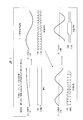
- FIG. 3 is an explanatory view showing a drive waveform output example of the motor M.
- the U phase and the UB phase are illustrated, and the other V phase, VB phase, W phase, and WB phase are omitted. ing.
- the semiconductor integrated circuit device 1 performs drive control of the motor M by changing the frequency and ON duty of a PWM (Pulse ⁇ Width Modulation) waveform output as a motor drive waveform according to the motor rotation speed.
- the sin waveform described in the upper part of the U phase / UB phase is a waveform indicating the rotation state of the motor M.
- the motor drive waveform may be switched in accordance with the rotational speed of the motor.
- the motor waveform output circuit 7 is configured to be able to switch the motor drive waveform to be output by an instruction from the CPU (setting to a register) or a motor rotation speed determination circuit 9.
- the resolver signal (sin wave, cos wave) output from the resolver 2 is converted into a digital value by the R / D converter 3 (step S101).
- the current value of the motor M is converted into a digital value by the A / D converter 8 (step S102).
- the R / D conversion interface 102 receives the digital signal converted by the R / D converter 3 (step S103), and outputs the digital signal to the resolver value correction calculation circuit 5 and the motor rotation speed determination circuit 9 (the one-dot chain line in FIG. 4). Processing route).
- the motor rotation speed determination circuit 9 determines the rotation speed of the motor from the frequency of the signal converted into a digital value by the R / D converter 3 input to the R / D conversion interface 4.
- the motor rotation speed determination circuit 9 determines that the rotation speed of the motor M is stopped to low speed (smaller than a predetermined rotation speed)
- the following steps S104 to S106 are performed by software processing by the CPU (FIG. 4 is a command signal between the motor rotation speed determination circuit and the CPU indicated by a thin solid line 4).
- the motor rotational resistance is relatively high and the frictional resistance between the tire and the road surface causes the motor driving waveform to be supplied to the motor M to have a lower frequency and an increased current amount.
- Transient processing such as increasing the rotational torque of M is required. Since such transient processing has large individual differences and ambient environment differences, it is possible to match the characteristics of each solid / peripheral environment by software processing.
- the processing of the following steps S104 to S107 is hardware processing in each circuit ( (A command signal between the motor rotation speed determination circuit and the resolver value correction calculation circuit, etc., indicated by a thin solid line in FIG. 4).
- the rotational resistance of the motor and the road surface friction resistance are relatively low, and processing according to the individual / ambient environment difference is relatively unnecessary, and the motor drive waveform is applied to the motor at an appropriate timing according to the rotational angle of the motor. Therefore, it is preferable to use hardware processing.
- the motor rotation speed determination circuit 9 determines the motor rotation speed, depending on the motor rotation angle.
- the processing in steps S104 to S107 is performed in each circuit so as to supply a motor driving waveform that generates a rotational torque of the motor in a direction opposite to the rotation of the tire or the rotor of the motor at an appropriate timing.
- the determination boundary value is stored in a non-volatile memory such as a flash memory of the memory unit 12.
- the CPU 10 may store the determination boundary value in the register R 1 of the motor rotation speed determination circuit 9 in the initialization operation of the semiconductor integrated circuit device 1. Further, the determination boundary is not limited to coincide with the low speed / medium speed / high speed rotation boundary shown in FIG.
- steps S104 to S107 will be described as the operation of each circuit when it is determined that the rotational speed of the motor is medium speed to high speed (greater than a predetermined rotational speed).
- the resolver value correction calculation circuit 5 calculates a resolver correction value in the digital signal input from the R / D conversion interface 4 or reads it from the memory unit 12 via the bus 13 (step S104), and from the R / D conversion interface 4.
- the position data indicating the rotation angle of the motor is calculated by adding / subtracting the correction value to / from the input digital value (step S105).
- the motor control arithmetic circuit 6 includes information on acceleration / deceleration braking from an accelerator or brake (not shown), position data calculated by the resolver value correction arithmetic circuit 5, and the A / D converter 8 is digital.
- a current command value is calculated from the converted motor current value, the motor current command value, and the like (step S106), and is output to the motor waveform output circuit 7.
- the motor waveform output circuit 7 generates a motor drive waveform from the input current command value and outputs it to the power module PM that drives the motor M (step S107).
- the dotted line indicates the processing path of steps S104 and S105
- the thin solid line indicates the processing path of steps S106 and S107
- the alternate long and short dash line indicates the path of the motor rotation speed signal
- the thick solid line indicates the software. The route in the process is shown.
- the resolver value correction calculation circuit 5 may perform the resolver value correction calculation processing even when the motor rotation speed is determined to be stopped to low speed and the motor drive control is performed by CPU software processing. In that case, instead of the resolver value correction calculation in the CPU, the resolver correction value in the resolver value correction calculation circuit 5 is controlled to be output to the CPU via the bus 13.
- FIG. 5 is an explanatory diagram showing a configuration example of the motor control arithmetic circuit 6.
- the motor control arithmetic circuit 6 includes PID control modules 14 and 15, a two-phase three-phase conversion module 16, a three-phase two-phase conversion module 17, a PWM conversion module 18, and adders / subtractors 19 and 20 as shown in the figure. Yes.
- the motor control calculation circuit 6 outputs information from the acceleration / deceleration braking, position data (correction ⁇ ) indicating the rotation angle of the motor calculated by the resolver value correction calculation circuit 5, and output from the A / D converter 8.
- Motor current values (u, v, w) to be output and motor current command values output from the CPU 10 ('d-axis current command value,' q-axis current command value), etc.
- the PWM conversion module 18 converts the frequency / duty for motor control with respect to the reference PWM waveform, and outputs the motor waveform as the current command value for each U / V / W. Output to the force circuit 7.
- This current command value generates a motor drive waveform that generates a rotational torque in the forward direction with respect to the rotation of the motor in the acceleration braking of the automobile, and a rotational torque in the opposite direction to the rotation of the motor in the deceleration braking.
- the motor drive waveform to be generated is generated.
- the motor waveform output circuit 7 outputs the motor drive waveform shown in FIG. 3 to the power module PM from the current command value calculated by the motor control calculation circuit 6.
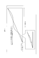
- FIG. 6 is an image diagram that is extremely expressed for easy understanding of an ideal resolver value and a resolver value including an error.
- the resolver value obtained by the resolver 2 is different from the ideal value shown by the dotted line in FIG. 6 in terms of mechanical error such as the shape, size, and variation of the resolver, electrical variation such as winding, wiring, and stray capacitance, and eccentricity. Due to variations in attachment such as zero point deviation, the value always includes an error as shown by a solid line in FIG. Since the resolver value is a digital value, it is stepped as shown in the enlarged view at the lower left of FIG.
- FIG. 7 is an explanatory diagram showing a timing example of energization switching (for example, 120 °) at the time of high motor rotation due to a compare match with a resolver value including an error.
- U-phase normal phase (U), V-phase normal phase (V), W-phase normal phase (W), U-phase reverse phase (UB), V-phase reverse phase (VB), W-phase reverse phase (WB) Is an output signal from the semiconductor integrated circuit device 1. These output signals control the U phase, V phase, and W phase of the motor M via the power module PM.
- the resolver value when the resolver value reaches the preset compare value, the energized phase in the motor M is switched, and the resolver value including the error (shown by the solid line in FIG. 7) and the error are included.
- the ideal resolver value shown by the dotted line in FIG. 7
- the motor switching timing differs, which becomes an error, and the advancement and delay of the energization switching Occurs, and the magnetic field generated by the current flowing through the coils of the U, V, and W phases disturbs the rotation of the rotor of the motor, and the motor M does not move smoothly, resulting in a decrease in rotational efficiency. It will be.
- FIG. 8 is an explanatory diagram showing an enlarged portion where the energization switching in FIG. 7 is performed.
- the resolver value is corrected by software from, for example, correction data (such as past period data such as at low rotation).
- correction data such as past period data such as at low rotation
- the correction calculation update frequency and calculation processing time by software become a problem. If the calculation processing time is long and the correction calculation update frequency is low, sufficient correction cannot be performed and an error remains (stepped waveform indicated by a thin solid line).
- the error ratio is relatively small. However, when the motor rotates at a high speed, the error ratio becomes relatively large, and energization switching control including a calculation error is performed.
- 8 is an output signal from the semiconductor integrated circuit device 1 such as the U-phase positive phase (U) in FIG.
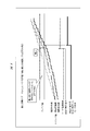
- FIG. 9 is an explanatory diagram showing an outline of the operation of the resolver value correction technique by the semiconductor integrated circuit device 1 of the present invention.
- the resolver value is sequentially corrected by hardware processing performed by the resolver value correction calculation circuit 5.
- the successive conversion logic of the resolver value correction calculation circuit 5 calculates a correction value from the input rotation period and resolver value, and outputs a corrected resolver value by adding or subtracting the correction value to or from the resolver value.
- the error is greatly reduced, and the resolver value including the error (shown by a solid line in FIG. 9) can be brought close to the ideal resolver value (shown by a dotted line in FIG. 9).
- the motor ideal waveform and the sequentially corrected motor waveform in FIG. 9 are output signals from the semiconductor integrated circuit device 1 such as the U-phase positive phase (U) in FIG.
- the CPU needs to operate at about 222 MHz. Even in such a case, interrupt processing is frequently applied and timing constraints are generated. Therefore, if the interrupt is to be reduced to about 10% or less of the CPU load, the CPU needs an operation speed of about 1 GHz. Become. The operating speed of the CPU is technically possible, but power consumption increases. When considering motor control in an electric vehicle, there are periods during which the motor rotates at a medium speed to a high speed and periods during which the motor rotates at a low speed, and the CPU is excessive during the stop-low speed rotation period. Since it has processing capability, wasteful power consumption of the CPU occurs.
- FIG. 10 shows the difference in the maximum number of rotations of the motor between the case where the correction processing by software when the CPU operating speed is 100 MHz and the case where the hardware processing by the resolver value correction arithmetic circuit 5 is performed. It is explanatory drawing.
- the motor rotation speed is about 48.8 Hz (about 3000 rpm), and when the CPU load factor is 100% (only correction processing is performed by software). In this case, the motor rotation speed is about 488 Hz (about 30000 rpm).
- the motor rotation speed can be significantly increased to about 1627 Hz (about 98000 rpm).
- FIG. 11 is an explanatory diagram showing a comparative example of current consumption when the resolver value is sequentially corrected. This is a case where the operating frequency is considered to be equal to the current.
- the processing speed of the CPU must be increased to about 1 GHz as described above, and the current is consumed significantly. Become.
- the operating frequency of the CPU is determined in consideration of the power consumption in the semiconductor integrated circuit device 1, and the stop to low speed is determined.
- the motor torque can be controlled according to the situation by software control, and in the low-speed, medium-speed, and high-speed motor rotation ranges, control corresponding to each process is switched by hardware. By doing so, it becomes possible to optimize the power consumption in the semiconductor integrated circuit device 1.
- the resolver value correction arithmetic circuit 5, the motor control arithmetic circuit 6, and the motor waveform output circuit 7 do not perform a synchronous operation with a clock for operating the CPU or the like, but according to an input from the R / D converter 3. Therefore, the power consumption can be further reduced.
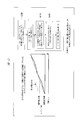
- FIG. 12 is an explanatory diagram showing an example of a technique for correcting a resolver value by the resolver value correction calculation circuit 5.
- the resolver value correction arithmetic circuit 5 uses a Z-phase signal Z (Z-phase input), a compare signal, a timer, etc. to generate a fixed period, and an ideal resolver value (dotted line). The correction value is calculated for each count from the difference between the actual resolver value (solid line).
- an error is obtained in advance from the resolver value for the actual revolution in the resolver 2 and an ideal value obtained from the initial rotation position of the motor and the elapsed rotation time, and stored as error A (for example, in the memory unit 12).
- An error between the ideal value read from the memory unit 12 and the resolver value is calculated as an error B every arbitrary fixed period (which should be as short as possible) (processing 2).
- the subsequent correction value is calculated from the ratio between the error A and the error B, and is reflected as a correction value for the subsequent resolver value (processing 3).
- the ideal value from the memory unit 12 is read out by reading out the ideal value corresponding to the rotational position of the motor every arbitrary fixed period, or by correcting the ideal value for one revolution of the motor from the memory unit 12 by a resolver value correction (not shown). It may be read out to a memory such as a RAM provided in the arithmetic circuit 5.
- the reverse phase (WB) is an output signal from the semiconductor integrated circuit device 1 as in FIG. These output signals control the U phase, V phase, and W phase of the motor M via the power module PM.
- the timing of the energization switching can be made closer to the ideal, so that the rotation of the motor M can be efficiently and further increased.
- the motor can be smoothly and efficiently controlled from the motor stop state (0 rpm) to the high speed rotation (10000 rpm or more).
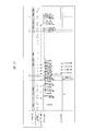
- the semiconductor integrated circuit device has two CPUs (10-1 and 10-2), the first CPU and the second CPU, and the clock supplied to the functional modules of the CPU and other semiconductor integrated circuit devices.
- the output of the R / D converter 3 that converts the output value of the resolver 2 that detects the rotation of the motor M such as an electric vehicle into a digital value is input to the R / D conversion interface 4, and the R / D conversion interface 4
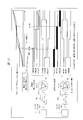
- the R / D conversion interface 4 When the rotation speed of the motor M is not more than the first rotation speed (control switching rotation speed) from the stop (timing t0 to t1), the R / D conversion interface 4 is supplied to the motor rotation speed determination circuit 9 as rotation speed information. Notifies the interrupt controller 11 every time a signal is input from the resolver, and the interrupt controller 11 notifies the CPU 10-1 of the occurrence of an interrupt.
- the CPU 10-1 executes an interrupt processing program for generating motor control information for each interrupt notification, and corrects the resolver value converted into a digital value and controls for controlling the rotation of the motor M based on the corrected resolver value. Calculation is performed to generate a current command value.
- the motor rotational speed determination circuit 9 notifies the interrupt controller 11 (timing t1).
- the interrupt controller 11 notifies the CPU 10-1 of the occurrence of an interrupt, and the CPU 10-1 instructs the frequency divider 101 and the power supply circuit 102 to supply power and clock to the CPU 10-2.
- a program for correcting the resolver value stored in the memory unit 12 is transferred to the local memory 103 of the CPU 10-2 ( Timing t2).
- the frequency of the clock supplied to the CPU 10-2 is the same operating frequency as the CPU 10-1 in accordance with the frequency at which the resolver value is input from the R / D conversion interface 4 and the execution of the resolver value correction program. Or less.
- the CPU 10-1 sends a notification (not shown) to the R / D conversion interface 4, and the R / D conversion interface 4 stops outputting the resolver value to the bus 13, and the CPU 10- 2 is switched to directly output to 2, and further, the interrupt controller 11 is notified to stop interrupt generation according to the output of the resolver value by the R / D conversion interface 11 (timing t3).
- the CPU 10-2 corrects the resolver value by fetching and executing the resolver value correction program stored in the local memory 103, and stores the corrected resolver value in the shared memory 103 with the CPU 10-1 (timing t3 To t4).
- the CPU 10-2 While the motor M is rotating at the control switching rotation speed or higher (timing t3 to t4), the CPU 10-2 performs correction processing every time a resolver value is input from the R / D conversion interface 4, and the shared memory To 103.
- the CPU 10-1 generates a current command value by executing a control calculation program for controlling the rotation of the motor M based on the corrected resolver value stored in the shared memory 103, and an operation control program for the semiconductor integrated circuit device as a whole. Execute.
- the CPU 10-2 For storing the corrected resolver value in the shared memory 103 by the CPU 10-2, the CPU 10-2 sets a flag every time it is stored, and the CPU 10-1 monitors the flag by polling and resets the flag every time it is read. Alternatively, an interrupt notification may be generated every time the corrected resolver value is stored.
- the program for correcting the resolver value is transferred to the local memory 103, and the CPU 10-2 is configured to fetch the program from the local memory, so that the CPU 10-2 fetches the program to the memory unit 12. Access competition to the bus 13 can be avoided.
- the motor rotation speed determination circuit 9 notifies the interrupt controller 11 (timing t4).
- the interrupt controller 11 notifies the CPU 10-1 that an interrupt has occurred.
- the CPU 10-1 makes a notification (not shown) to the R / D conversion interface, switches to output the resolver value to the bus 13, and switches to generate an interrupt for each input of the resolver value.
- the CPU 10-1 instructs the CPU 10-2 to stop executing the resolver value correction program and the frequency divider 101 to stop the clock supply to the CPU 10-2 (timing t5).
- the power supply may be stopped after the motor M reaches the second rotation speed (power supply cutoff speed) lower than the control switching rotation speed (timing t6).
- the local memory 103 stops the power supply until it reaches the control switching rotational speed for the first time, and after reaching the control switching rotational speed and the transfer of the resolver value correction program, for example, the engine stop (or power of the automobile) By controlling so that the power supply continues until (OFF), it is possible to reduce the power consumption required for the transfer of the resolver value correction program.
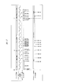
- the CPU 10-2 is always supplied with the power and the clock during the operation of the semiconductor integrated circuit device regardless of the rotational speed of the motor M.
- the CPU 10-1 transfers the resolver value correction program executed by the CPU 10-2 from the memory unit 12 to the local memory 103.
- the CPU 10-1 sets the frequency of the clock supplied to the CPU 10-2 in the frequency divider 101 (128 kHz).
- the R / D conversion interface 4 outputs the resolver value to the CPU 10-2, and the CPU 10-2 fetches the resolver value correction program from the local memory 103 and stores the corrected resolver value in the shared memory 103.
- the motor rotation speed determination circuit 9 determines the rotation speed of the motor M, and in response to detection that the first rotation speed has been reached (timing tb 1), the interrupt controller 11. In response to the interrupt notification from the interrupt controller 11, the CPU 10-1 sets a change in the frequency of the clock supplied to the CPU 10-2 to the frequency divider 101 (128 kHz ⁇ 4 MHz).
- the frequency of the clock supplied to the CPU 10-2 is lowered according to the rotation speed of the motor M detected by the motor rotation speed determination circuit 9 (timing tb2).
- the output from the R / D conversion interface 4 and the resolver in the CPU 10-2 are changed by gradually changing the frequency of the clock supplied to the CPU 10-2 according to the rotational speed of the motor M.
- the value correction program it becomes possible to optimize the power consumption in the CPU 10-2.
- the CPU 10-1 can perform the control described above in the paragraph numbers.
- the description of the configuration of the semiconductor integrated circuit device shown in FIG. 14 does not mention the change of the clock frequency supplied while the CPU 10-2 is operating, but the configuration of the semiconductor integrated circuit device shown in FIG. Similarly to the above, it is naturally possible to optimize the power consumption in the CPU 10-2 by performing control to increase or decrease the clock frequency stepwise according to the rotational speed of the motor M.
- control technology for a motor used in an electric vehicle or the like is described. Is possible.
Landscapes
- Engineering & Computer Science (AREA)
- Power Engineering (AREA)
- Transportation (AREA)
- Mechanical Engineering (AREA)
- Chemical & Material Sciences (AREA)
- Combustion & Propulsion (AREA)
- Physics & Mathematics (AREA)
- General Physics & Mathematics (AREA)
- Control Of Electric Motors In General (AREA)
- Control Of Ac Motors In General (AREA)
- Control Of Motors That Do Not Use Commutators (AREA)
- Transmission And Conversion Of Sensor Element Output (AREA)
- Electric Propulsion And Braking For Vehicles (AREA)
Abstract
Description
図1は、電気自動車やハイブリッド自動車(以下、電気自動車などという。)に用いられるモータ駆動システムの構成例を示すブロック図である。
実施の形態2では、実施の形態1とは相違し、レゾルバ値の補正からモータMの制御にかけてを複数のCPUにより機能分割し、全体として低周波数・低消費電力で実現するための構成について説明する。本実施の形態での制御にかかる信号線は、図中、破線で示している。
Claims (15)
- モータの回転速度を判別するモータ回転速度判定回路を備え、
前記モータの回転速度に応じて、モータ駆動波形をソフトウェア処理により生成するかハードウェア処理により生成するかを切り替え可能に構成したことを特徴とする半導体集積回路装置。 - 請求項1記載の半導体集積回路装置において、
前記モータ回転速度判定回路はモータの回転速度の判別境界となる値を保持し、
前記モータの回転速度が前記値よりも低い場合は前記ソフトウェア処理により前記モータ駆動波形を生成し、前記値よりも高い場合は前記ハードウェア処理により前記モータ駆動波形を生成するように切り替えを行うことを特徴とする半導体集積回路装置。 - 請求項2記載の半導体集積回路装置において、
デジタル信号に変換されたモータに取り付けられたレゾルバから出力されたレゾルバ信号をカウントアップした誤差を含んだレゾルバ値を、前記モータの回転速度が前記値よりも低い場合はCPUのソフトウェア処理により逐次補正し、前記モータの回転速度が前記値よりも高い場合は前記ハードウェア処理によって逐次補正するレゾルバ値補正演算部を備えたことを特徴とする半導体集積回路装置。 - 請求項3記載の半導体集積回路装置において、
前記レゾルバ値補正演算部は、
前記レゾルバの1周期分における誤差を含んだレゾルバ値と誤差を含まない基準レゾルバ値との差からなる第1の誤差補正データを格納するデータ格納部と、
前記第1の誤差補正データに基づいて、誤差を含んだ前記レゾルバ値の補正処理を行うレゾルバ値補正演算回路とを備え、
前記レゾルバ値補正演算回路は、
入力された誤差を含んだレゾルバ値に、前記第1の誤差補正データを加減算し、前記レゾルバの1周期を2以上に分割した任意の周期毎での誤差を含んでいないレゾルバ値と誤差を含んだレゾルバ値とのずれを第2の誤差補正データとして算出し、前記第2の誤差補正データと前記第1の誤差補正データとの比率を比較して、第3の誤差補正データとして、次のレゾルバ値に反映させる処理を行うことを特徴とする半導体集積回路装置。 - 請求項4記載の半導体集積回路装置において、
前記レゾルバ値補正演算回路は、データフロー動作を行うハードウェア構成であることを特徴とする半導体集積回路装置。 - 請求項3~5のいずれか1項に記載の半導体集積回路装置において、
前記モータを駆動する駆動制御信号を発生するモータ駆動波形を生成するモータ制御部を備え、
前記モータ制御部は、
前記レゾルバ値補正演算部が補正したレゾルバ値から、前記モータの位置データを算出し、前記位置データ、前記モータに流れるモータ電流値、およびモータ電流指令値から電流指令値を演算し、前記電流指令値からモータ駆動波形を生成することを特徴とする半導体集積回路装置。 - 請求項6記載の半導体集積回路装置において、
前記モータの回転速度によってモータ駆動波形を切り替える制御を行うモータ回転速度判定回路を備えたことを特徴とする半導体集積回路装置。 - 第1のCPUと第2のCPUとモータ回転速度判定回路を備え、
前記第1のCPUは、前記モータ回転速度判定回路の出力がモータの回転速度が第1回転速度以下であることを示す場合は、レゾルバから出力されたレゾルバ値の補正処理と補正後のレゾルバ値に応じたモータの制御信号生成処理とを行い、
前記モータ回転速度判定回路の出力が前記モータの回転速度が第1回転速度より高いことを示すことに応じて、前記第2のCPUがレゾルバ値の補正処理を行い、前記第1のCPUは前記第2のCPUが行った補正後のレゾルバ値に応じたモータの制御信号生成処理とを行うよう切り替えることを特徴とする半導体集積回路装置。 - 請求項8記載の半導体集積回路装置において、
前記モータの回転速度が第1回転速度以下である間、前記第2のCPUへのクロック供給を停止し、前記モータの回転速度が第1回転速度より高くなることに応じて前記第2のCPUへのクロック供給を行う制御を行うクロック生成回路をさらに有することを特徴とする半導体集積回路装置。 - 請求項9記載の半導体集積回路装置において、
前記第2のCPUへのクロック供給が停止されている期間において、前記第2のCPUへ電源の供給を停止する制御を行う電源回路をさらに有することを特徴とする半導体集積回路装置。 - 請求項9記載の半導体集積回路装置において、
前記モータの回転速度が第1回転速度にいたるまで、および前記モータの回転速度が第1回転速度より高くなった後に前記第1回転速度よりも遅い第2回転速度にいたったことに応じて、前記第2のCPUへの電源の供給を停止する制御を行う電源回路をさらに有することを特徴とする半導体集積回路装置。 - 請求項8~11のいずれか1項に記載の半導体集積回路装置において、
前記第2のCPUに接続される第1メモリを有し、
前記第2のCPUは前記レゾルバ値の補正処理を行うためのプログラムを前記第1メモリからフェッチすることを特徴とする半導体集積回路装置。 - 請求項12記載の半導体集積回路装置において、
前記第1のCPUに接続される不揮発性メモリを有し、
前記第1のCPUは、実行すべきプログラムの命令を前記不揮発性メモリからフェッチし、前記第2のCPUが実行する前記レゾルバ値の補正処理プログラムは前記不揮発性メモリから前記第1メモリへ転送されることを特徴とする半導体集積回路装置。 - 第1のCPUと第2のCPUとモータの回転速度を判別するモータ回転速度判定回路とクロック供給回路とを有し、
前記第1のCPUは、レゾルバから出力されたレゾルバ値の補正処理を行い、
前記第2のCPUは、補正後のレゾルバ値に応じたモータの制御信号生成処理を行い、
前記第2のCPUは、前記モータの回転速度に応じて、前記クロック供給回路から前記第1のCPUへ供給するクロックの周波数を変更する制御を行うことを特徴とする半導体集積回路装置。 - 請求項14記載の半導体集積回路装置において、
前記第1のCPUに接続される第1メモリと、前記第2のCPUに接続される不揮発性メモリとを有し、
前記第1のCPUは前記レゾルバ値補正処理用のプログラムを前記第1メモリからフェッチし、
前記第2のCPUは前記モータ制御信号生成処理用のプログラムを前記不揮発性メモリからフェッチし、
前記レゾルバ値補正処理用プログラムは、前記不揮発性メモリから前記第1メモリへ転送されることを特徴とする半導体集積回路装置。
Priority Applications (6)
| Application Number | Priority Date | Filing Date | Title |
|---|---|---|---|
| CN201080009769.XA CN102334277B (zh) | 2009-03-27 | 2010-02-10 | 半导体集成电路器件 |
| US13/258,544 US8633667B2 (en) | 2009-03-27 | 2010-02-10 | Semiconductor integrated circuit device |
| JP2011505922A JP5511791B2 (ja) | 2009-03-27 | 2010-02-10 | 半導体集積回路装置 |
| EP10755765.4A EP2413495B1 (en) | 2009-03-27 | 2010-02-10 | Semiconductor integrated circuit device |
| US14/108,022 US9221357B2 (en) | 2009-03-27 | 2013-12-16 | Semiconductor integrated circuit device |
| US14/953,136 US9630523B2 (en) | 2009-03-27 | 2015-11-27 | Semiconductor integrated circuit device |
Applications Claiming Priority (2)
| Application Number | Priority Date | Filing Date | Title |
|---|---|---|---|
| JP2009-078732 | 2009-03-27 | ||
| JP2009078732 | 2009-03-27 |
Related Child Applications (2)
| Application Number | Title | Priority Date | Filing Date |
|---|---|---|---|
| US13/258,544 A-371-Of-International US8633667B2 (en) | 2009-03-27 | 2010-02-10 | Semiconductor integrated circuit device |
| US14/108,022 Continuation US9221357B2 (en) | 2009-03-27 | 2013-12-16 | Semiconductor integrated circuit device |
Publications (1)
| Publication Number | Publication Date |
|---|---|
| WO2010109964A1 true WO2010109964A1 (ja) | 2010-09-30 |
Family
ID=42780660
Family Applications (1)
| Application Number | Title | Priority Date | Filing Date |
|---|---|---|---|
| PCT/JP2010/051916 Ceased WO2010109964A1 (ja) | 2009-03-27 | 2010-02-10 | 半導体集積回路装置 |
Country Status (6)
| Country | Link |
|---|---|
| US (3) | US8633667B2 (ja) |
| EP (1) | EP2413495B1 (ja) |
| JP (3) | JP5511791B2 (ja) |
| KR (1) | KR101617486B1 (ja) |
| CN (2) | CN102334277B (ja) |
| WO (1) | WO2010109964A1 (ja) |
Cited By (3)
| Publication number | Priority date | Publication date | Assignee | Title |
|---|---|---|---|---|
| WO2012077752A1 (ja) * | 2010-12-10 | 2012-06-14 | アイシン・エィ・ダブリュ株式会社 | 制御装置 |
| WO2014064836A1 (ja) | 2012-10-26 | 2014-05-01 | ルネサスエレクトロニクス株式会社 | モータ制御装置及びモータ駆動装置 |
| JP2020148122A (ja) * | 2019-03-12 | 2020-09-17 | 株式会社デンソーテン | 制御装置および制御方法 |
Families Citing this family (10)
| Publication number | Priority date | Publication date | Assignee | Title |
|---|---|---|---|---|
| US9780718B2 (en) * | 2010-11-02 | 2017-10-03 | Whirlpool Corporation | Portable appliance motor control with speed-based current limitation |
| JP5925711B2 (ja) * | 2013-02-20 | 2016-05-25 | 浜松ホトニクス株式会社 | 検出器、pet装置及びx線ct装置 |
| JP2015136272A (ja) * | 2014-01-20 | 2015-07-27 | ルネサスエレクトロニクス株式会社 | 半導体デバイス及び駆動装置 |
| DE102014201758A1 (de) * | 2014-01-31 | 2015-08-06 | Robert Bosch Gmbh | Steuervorrichtung für eine elektromaschine, verfahren und motorsteuerung |
| JP5733447B1 (ja) | 2014-03-13 | 2015-06-10 | 株式会社昭和螺旋管製作所 | インターロックチューブの製造方法、及び、その製造装置 |
| US9438159B2 (en) * | 2014-06-26 | 2016-09-06 | Nidec Motor Corporation | System and method for detecting and controlling a motor |
| JP2018064340A (ja) * | 2016-10-12 | 2018-04-19 | ソフトロニクス株式会社 | モータ制御装置 |
| JP6776179B2 (ja) * | 2017-05-25 | 2020-10-28 | ルネサスエレクトロニクス株式会社 | モータ制御システム及び半導体装置 |
| JP6975632B2 (ja) * | 2017-12-21 | 2021-12-01 | ルネサスエレクトロニクス株式会社 | 半導体装置及びその回転異常検出方法 |
| JP7131431B2 (ja) * | 2019-02-25 | 2022-09-06 | トヨタ自動車株式会社 | 制御装置およびそのリセット方法 |
Citations (7)
| Publication number | Priority date | Publication date | Assignee | Title |
|---|---|---|---|---|
| JP2004152441A (ja) * | 2002-10-31 | 2004-05-27 | Toshiba Corp | ディスク記憶装置及び同装置におけるスピンドルモータの駆動電圧制御方法 |
| JP2004222448A (ja) * | 2003-01-16 | 2004-08-05 | Toyota Motor Corp | モータ制御装置 |
| JP2006262582A (ja) * | 2005-03-16 | 2006-09-28 | Ricoh Co Ltd | 搬送装置および画像形成装置 |
| JP2007020383A (ja) | 2005-06-09 | 2007-01-25 | Toyota Motor Corp | 車両の制御装置および車両 |
| JP2007033412A (ja) * | 2005-07-29 | 2007-02-08 | Nsk Ltd | 位置検出器の誤差パラメータ抽出装置および誤差補正機能を備える位置検出器 |
| JP2007108861A (ja) * | 2005-10-11 | 2007-04-26 | Canon Inc | プリンタ装置 |
| JP2007267449A (ja) * | 2006-03-27 | 2007-10-11 | Nsk Ltd | モータ駆動制御回路及びモータ駆動制御方法 |
Family Cites Families (17)
| Publication number | Priority date | Publication date | Assignee | Title |
|---|---|---|---|---|
| JPS5375613A (en) * | 1976-12-15 | 1978-07-05 | Hitachi Ltd | Motor controlling apparatus |
| JP2582071B2 (ja) * | 1987-05-19 | 1997-02-19 | 株式会社日立製作所 | パルス幅変調方式インバ−タの制御装置 |
| JPH0450452A (ja) * | 1990-06-20 | 1992-02-19 | Nissan Motor Co Ltd | 車両用エンジンの制御装置 |
| JPH0984208A (ja) * | 1995-09-14 | 1997-03-28 | Denso Corp | 電気自動車用制御装置 |
| JP3610687B2 (ja) * | 1995-12-12 | 2005-01-19 | トヨタ自動車株式会社 | 内燃機関の始動制御装置およびその制御方法 |
| IT1289397B1 (it) * | 1996-10-25 | 1998-10-02 | Procond Elettronica Spa | Macchina da esercitazione fisica con circuiti di controllo perfezionati |
| US6654648B2 (en) * | 2000-04-03 | 2003-11-25 | Toyota Jidosha Kabushiki Kaisha | Technique of monitoring abnormality in plurality of CPUs or controllers |
| JP2004045286A (ja) * | 2002-07-12 | 2004-02-12 | Denso Corp | レゾルバ補正方法 |
| JP4079077B2 (ja) * | 2003-11-27 | 2008-04-23 | トヨタ自動車株式会社 | 車両用走行制御装置 |
| US7633256B2 (en) * | 2005-05-04 | 2009-12-15 | Lexmark International, Inc. | Encoder eccentricity correction for motion control systems |
| US7828093B2 (en) | 2005-12-26 | 2010-11-09 | Toyota Jidosha Kabushiki Kaisha | Vehicle controller, vehicle and vehicle control method |
| CN101647190B (zh) * | 2007-03-30 | 2012-03-07 | 新电元工业株式会社 | 无刷电机控制装置和无刷电机控制方法 |
| JP4783752B2 (ja) | 2007-04-04 | 2011-09-28 | 愛三工業株式会社 | レゾルバ |
| JP2008278652A (ja) * | 2007-04-27 | 2008-11-13 | Toyota Motor Corp | 駆動力制御装置 |
| JP4949943B2 (ja) * | 2007-06-18 | 2012-06-13 | 愛三工業株式会社 | レゾルバ |
| US8269435B2 (en) * | 2007-11-30 | 2012-09-18 | Ricoh Company, Ltd | Motor control unit, motor control method and image forming apparatus |
| JP5456608B2 (ja) * | 2010-07-20 | 2014-04-02 | トヨタ自動車株式会社 | モータの制御装置および制御方法 |
-
2010
- 2010-02-10 CN CN201080009769.XA patent/CN102334277B/zh active Active
- 2010-02-10 EP EP10755765.4A patent/EP2413495B1/en active Active
- 2010-02-10 US US13/258,544 patent/US8633667B2/en not_active Expired - Fee Related
- 2010-02-10 KR KR1020117022545A patent/KR101617486B1/ko active Active
- 2010-02-10 JP JP2011505922A patent/JP5511791B2/ja not_active Expired - Fee Related
- 2010-02-10 WO PCT/JP2010/051916 patent/WO2010109964A1/ja not_active Ceased
- 2010-02-10 CN CN201410264922.3A patent/CN104022715B/zh active Active
-
2013
- 2013-12-16 US US14/108,022 patent/US9221357B2/en active Active
-
2014
- 2014-03-25 JP JP2014061139A patent/JP5736483B2/ja active Active
-
2015
- 2015-04-20 JP JP2015085949A patent/JP2015156796A/ja active Pending
- 2015-11-27 US US14/953,136 patent/US9630523B2/en active Active
Patent Citations (7)
| Publication number | Priority date | Publication date | Assignee | Title |
|---|---|---|---|---|
| JP2004152441A (ja) * | 2002-10-31 | 2004-05-27 | Toshiba Corp | ディスク記憶装置及び同装置におけるスピンドルモータの駆動電圧制御方法 |
| JP2004222448A (ja) * | 2003-01-16 | 2004-08-05 | Toyota Motor Corp | モータ制御装置 |
| JP2006262582A (ja) * | 2005-03-16 | 2006-09-28 | Ricoh Co Ltd | 搬送装置および画像形成装置 |
| JP2007020383A (ja) | 2005-06-09 | 2007-01-25 | Toyota Motor Corp | 車両の制御装置および車両 |
| JP2007033412A (ja) * | 2005-07-29 | 2007-02-08 | Nsk Ltd | 位置検出器の誤差パラメータ抽出装置および誤差補正機能を備える位置検出器 |
| JP2007108861A (ja) * | 2005-10-11 | 2007-04-26 | Canon Inc | プリンタ装置 |
| JP2007267449A (ja) * | 2006-03-27 | 2007-10-11 | Nsk Ltd | モータ駆動制御回路及びモータ駆動制御方法 |
Non-Patent Citations (1)
| Title |
|---|
| See also references of EP2413495A4 * |
Cited By (10)
| Publication number | Priority date | Publication date | Assignee | Title |
|---|---|---|---|---|
| WO2012077752A1 (ja) * | 2010-12-10 | 2012-06-14 | アイシン・エィ・ダブリュ株式会社 | 制御装置 |
| US8836255B2 (en) | 2010-12-10 | 2014-09-16 | Aisin Aw Co., Ltd. | Control device |
| DE112011102997B4 (de) * | 2010-12-10 | 2016-11-03 | Aisin Aw Co., Ltd. | Steuerungsvorrichtung zur Steuerung einer Elektromotorantriebsvorrichtung |
| WO2014064836A1 (ja) | 2012-10-26 | 2014-05-01 | ルネサスエレクトロニクス株式会社 | モータ制御装置及びモータ駆動装置 |
| CN104756398A (zh) * | 2012-10-26 | 2015-07-01 | 瑞萨电子株式会社 | 马达控制装置以及马达驱动装置 |
| US20150270796A1 (en) * | 2012-10-26 | 2015-09-24 | Renesas Electronic Corporation | Motor control device and motor drive device |
| JP5951787B2 (ja) * | 2012-10-26 | 2016-07-13 | ルネサスエレクトロニクス株式会社 | モータ制御装置及びモータ駆動装置 |
| CN104756398B (zh) * | 2012-10-26 | 2018-02-23 | 瑞萨电子株式会社 | 马达控制装置以及马达驱动装置 |
| US10038396B2 (en) | 2012-10-26 | 2018-07-31 | Renesas Electronics Corporation | Motor control device and motor drive device |
| JP2020148122A (ja) * | 2019-03-12 | 2020-09-17 | 株式会社デンソーテン | 制御装置および制御方法 |
Also Published As
| Publication number | Publication date |
|---|---|
| US8633667B2 (en) | 2014-01-21 |
| KR20110131242A (ko) | 2011-12-06 |
| EP2413495A4 (en) | 2018-03-14 |
| JPWO2010109964A1 (ja) | 2012-09-27 |
| JP5511791B2 (ja) | 2014-06-04 |
| EP2413495B1 (en) | 2021-04-07 |
| JP2015156796A (ja) | 2015-08-27 |
| EP2413495A1 (en) | 2012-02-01 |
| US9630523B2 (en) | 2017-04-25 |
| CN102334277A (zh) | 2012-01-25 |
| CN104022715B (zh) | 2017-04-12 |
| US20160075255A1 (en) | 2016-03-17 |
| US20140114522A1 (en) | 2014-04-24 |
| US20120013281A1 (en) | 2012-01-19 |
| JP2014147287A (ja) | 2014-08-14 |
| KR101617486B1 (ko) | 2016-05-02 |
| US9221357B2 (en) | 2015-12-29 |
| JP5736483B2 (ja) | 2015-06-17 |
| CN104022715A (zh) | 2014-09-03 |
| CN102334277B (zh) | 2014-07-23 |
Similar Documents
| Publication | Publication Date | Title |
|---|---|---|
| JP5511791B2 (ja) | 半導体集積回路装置 | |
| US8159162B2 (en) | Motor control apparatus, vehicle fan drive apparatus, and motor control method | |
| JP6365112B2 (ja) | 車載電動機用の制御装置 | |
| US12537465B2 (en) | Motor control apparatus and motor control method | |
| JP5576722B2 (ja) | 過電圧抑制装置及びモータ駆動装置 | |
| JP5141149B2 (ja) | モータ制御装置およびそれを搭載する車両 | |
| JP5724977B2 (ja) | ブラシレスモータの制御システム | |
| CN104796046A (zh) | 半导体器件和驱动设备 | |
| JP7290434B2 (ja) | モータ駆動制御装置及びモータの駆動制御方法 | |
| JP5077106B2 (ja) | 電動機制御装置、制御方法 | |
| JP2008236892A (ja) | ブラシレスモータの制御装置 | |
| JP2004129379A (ja) | モータ制御装置、およびモータの駆動制御をコンピュータに実行させるためのプログラムを記録したコンピュータ読取り可能な記録媒体 | |
| JP2023119319A (ja) | モータ制御装置 | |
| JP6668933B2 (ja) | 自動車 | |
| JP2006288109A (ja) | サーボモータ制御装置 | |
| JP2012135103A (ja) | モータ駆動制御装置 | |
| JP5374145B2 (ja) | モータ制御装置 | |
| JP7176341B2 (ja) | モータ制御用の情報処理装置 | |
| WO2024162002A1 (ja) | 力率制御装置、力率制御方法、及び力率制御プログラム | |
| JP6058085B1 (ja) | 回転電機および回転電機の制御方法 | |
| JP2023094198A (ja) | ラジエータファンモータ制御装置 | |
| JP2010239809A (ja) | 回転電機制御装置 | |
| JP2020156291A (ja) | モータ駆動制御装置 | |
| JP2011097782A (ja) | 車両のモータ制御装置 |
Legal Events
| Date | Code | Title | Description |
|---|---|---|---|
| WWE | Wipo information: entry into national phase |
Ref document number: 201080009769.X Country of ref document: CN |
|
| 121 | Ep: the epo has been informed by wipo that ep was designated in this application |
Ref document number: 10755765 Country of ref document: EP Kind code of ref document: A1 |
|
| WWE | Wipo information: entry into national phase |
Ref document number: 2011505922 Country of ref document: JP |
|
| WWE | Wipo information: entry into national phase |
Ref document number: 13258544 Country of ref document: US |
|
| WWE | Wipo information: entry into national phase |
Ref document number: 2010755765 Country of ref document: EP |
|
| ENP | Entry into the national phase |
Ref document number: 20117022545 Country of ref document: KR Kind code of ref document: A |
|
| NENP | Non-entry into the national phase |
Ref country code: DE |