WO2010109936A1 - 電子部品及びその製造方法 - Google Patents
電子部品及びその製造方法 Download PDFInfo
- Publication number
- WO2010109936A1 WO2010109936A1 PCT/JP2010/050718 JP2010050718W WO2010109936A1 WO 2010109936 A1 WO2010109936 A1 WO 2010109936A1 JP 2010050718 W JP2010050718 W JP 2010050718W WO 2010109936 A1 WO2010109936 A1 WO 2010109936A1
- Authority
- WO
- WIPO (PCT)
- Prior art keywords
- coil
- conductor
- conductors
- electronic component
- stacking direction
- Prior art date
- Legal status (The legal status is an assumption and is not a legal conclusion. Google has not performed a legal analysis and makes no representation as to the accuracy of the status listed.)
- Ceased
Links
Images




Classifications
-
- H—ELECTRICITY
- H01—ELECTRIC ELEMENTS
- H01F—MAGNETS; INDUCTANCES; TRANSFORMERS; SELECTION OF MATERIALS FOR THEIR MAGNETIC PROPERTIES
- H01F17/00—Fixed inductances of the signal type
- H01F17/0006—Printed inductances
- H01F17/0013—Printed inductances with stacked layers
-
- H—ELECTRICITY
- H01—ELECTRIC ELEMENTS
- H01F—MAGNETS; INDUCTANCES; TRANSFORMERS; SELECTION OF MATERIALS FOR THEIR MAGNETIC PROPERTIES
- H01F17/00—Fixed inductances of the signal type
- H01F17/0006—Printed inductances
- H01F17/0013—Printed inductances with stacked layers
- H01F2017/002—Details of via holes for interconnecting the layers
Definitions
- the present invention relates to an electronic component and a manufacturing method thereof, and more specifically to an electronic component in which a coil is built in a laminated body and a manufacturing method thereof.
- FIG. 8 is an exploded perspective view of the multilayer body 112 of the multilayer chip inductor.
- the multilayer body 112 of the multilayer chip inductor is composed of magnetic layers 114 (114a to 114k), and incorporates a coil L.
- the magnetic layer 114 is a rectangular layer made of a magnetic material such as Ni—Cu—Zn-based ferrite, and is stacked so as to be arranged in this order from the upper side in the stacking direction.
- the coil L is constituted by a lead conductor 116 (116a, 116b), a coil conductor 118 (118a-118c), and a via-hole conductor b11-b14.
- the coil conductors 118a to 118c are linear conductors with one side of a rectangle having a number of turns of 3/4, and are provided on the magnetic layers 114e to 114g.
- the lead conductors 116a and 116b are respectively provided above or below the coil conductors 118a to 118c in the stacking direction, and specifically, provided on the magnetic layers 114d and 114h.
- Each lead conductor 116 serves to connect the coil L and an external electrode (not shown).
- the via-hole conductors b11 to b14 are respectively provided so as to penetrate the magnetic layers 114d to 114g in the stacking direction, and connect the lead conductor 116 and the coil conductor 118 adjacent in the stacking direction. Thereby, the helical coil L is comprised.
- the number of turns of the coil L can be changed without changing the design of the coil conductor 118. More specifically, the number of turns of the coil L can be increased by adding the magnetic layer 114 provided with the coil conductor 118 on the lower side in the stacking direction of the magnetic layer 114d. Further, the number of turns of the coil L can be reduced by removing the magnetic layer 114 located on the lower side in the stacking direction of the magnetic layer 114d.
- the number of turns of the coil L is decreased will be described as an example.
- the coil L shown in FIG. 8 has a turn number of 13/4.
- the magnetic layer 114l provided with the lead conductor 116c is replaced with a magnetic layer. What is necessary is just to insert between the body layer 114c and the magnetic body layer 114f.
- the magnetic layer 114m provided with the lead conductor 116d is replaced with What is necessary is just to insert between the magnetic body layer 114c and the magnetic body layer 114g.
- an object of the present invention is to provide an electronic component that does not require changing the shape of the lead conductor, the position of the via-hole conductor, and the manufacturing method thereof when changing the number of turns of the coil.
- An electronic component includes a stacked body in which a plurality of insulator layers are stacked, a spiral coil built in the stacked body, and an external surface provided on the surface of the stacked body.
- the coil is a coil conductor provided on the main surface on the upper side in the stacking direction of the insulator layer, and when viewed in plan from the stacking direction, the coil A plurality of coil conductors overlapping each other at a point, and a first via-hole conductor provided in the insulator layer, and when viewed in plan from the stacking direction, the plurality of coil conductors at the specific point A first via-hole conductor that overlaps and is electrically connected to the external electrode, and the insulator layer provided with the first via-hole conductor is provided with the coil conductor Said plural Provided above the insulator layer in the stacking direction, and the first via-hole conductor is connected to the coil conductor at a position other than the end of the coil conductor when viewed in plan from the stacking direction
- An electronic component manufacturing method is a method of manufacturing an electronic component including a multilayer body including a spiral coil and an external electrode provided on a surface of the multilayer body.
- a first via-hole conductor to be electrically connected, the first via-hole conductor overlapping the specific point when viewed in plan from the stacking direction, and the coil being desired Adjusting the number of the plurality of insulator layers on which the coil conductor is formed so as to have the number of turns, and laminating the plurality of insulator layers, and the plurality of insulators on which the coil conductor is formed Above the layer in the stacking direction
- the present invention it is not necessary to change the shape of the lead conductor, the position of the via-hole conductor, etc. when changing the number of turns of the coil.
- FIG. 1 is an external perspective view of an electronic component according to an embodiment of the present invention. It is a disassembled perspective view of the laminated body of the electronic component of FIG. It is a disassembled perspective view of the laminated body of the electronic component which concerns on a reference example. It is a disassembled perspective view of the laminated body of the electronic component of FIG. It is a disassembled perspective view of the laminated body of the electronic component which concerns on a modification. It is an external appearance perspective view of the electronic component which concerns on other embodiment. It is a disassembled perspective view of the laminated body of the electronic component of FIG. 10 is an exploded perspective view of a multilayer body of multilayer chip inductors described in Patent Document 1.
- FIG. 1 is an external perspective view of an electronic component according to an embodiment of the present invention. It is a disassembled perspective view of the laminated body of the electronic component of FIG. It is a disassembled perspective view of the laminated body of the electronic component which concerns on a reference example. It is a disassembled
- FIG. 1 is an external perspective view of the electronic components 10a and 10b.
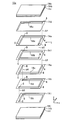
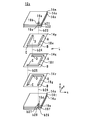
- 2 and 4 are exploded perspective views of the multilayer body 12a of the electronic component 10a.
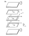
- FIG. 3 is an exploded perspective view of the multilayer body 12a ′ of the electronic component 10a ′ according to the reference example.
- the stacking direction of the electronic component 10a is defined as the z-axis direction
- the direction along the long side of the electronic component 10a is defined as the x-axis direction
- the direction along the short side of the electronic component 10a is defined as the y-axis direction.
- the electronic component 10a includes a rectangular parallelepiped laminated body 12a and two external electrodes 13 (13a, 13b) formed on the side surfaces (surfaces) of the laminated body 12a located at both ends in the x-axis direction. And.
- the laminated body 12a is configured by laminating magnetic layers 14 (14a to 14l) in this order in the z-axis direction, and incorporates a spiral coil L.
- the magnetic layer 14 is a rectangular insulating layer made of ferrite having magnetism (for example, Ni—Zn—Cu ferrite or Ni—Zn ferrite).
- the coil L includes lead conductors (internal conductors) 16 (16a, 16b), coil conductors (internal conductors) 18 (18a to 18d), and via-hole conductors b1 to b5.
- the lead conductor 16, the coil conductor 18, and the via-hole conductors b1 to b5 are made of, for example, a conductive material containing Ag as a main component.
- the coil conductors 18a to 18d are provided on the main surfaces on the positive direction side in the z-axis direction of the magnetic layers 14e to 14h, respectively.
- Each of the coil conductors 18 has a shape in which a part of the annular linear conductor is cut out, and has (n / n + 1) turns (3/4 turns in this embodiment). (N is a natural number).
- the coil conductor 18a has a “U” shape in which a long side located on the negative direction side in the y-axis direction is cut out.
- the coil conductor 18b has a “U” shape with a short side cut out on the positive side in the x-axis direction.
- the coil conductor 18c has a “U” shape in which a long side located on the positive direction side in the y-axis direction is cut out.
- the coil conductor 18d has a “U” shape with a short side cut out on the negative side in the x-axis direction.
- each of the coil conductors 18 passes through points A to D on the magnetic layer 14 at corners or ends.
- both ends of the coil conductor 18a are located at points B and C, and the corners of the coil conductor 18a are located at points A and D.
- Both ends of the coil conductor 18b are located at points A and B, and the corners of the coil conductor 18b are located at points C and D.
- Both ends of the coil conductor 18c are located at points A and D, and the corners of the coil conductor 18c are located at points B and C.
- Both ends of the coil conductor 18d are located at points C and D, and the corners of the coil conductor 18d are located at points A and B.
- the coil conductors 18a to 18d overlap each other at points A to D when viewed in plan from the z-axis direction.
- the coil conductors 18 having the above configuration overlap each other to form an annular (rectangular) track when viewed in plan from the z-axis direction. Points A to D are located at each corner of the trajectory.
- the lead conductor 16a is provided on the positive direction side in the z-axis direction from the coil conductor 18, and is provided on the main surface on the positive direction side in the z-axis direction of the magnetic layer 14d.
- the lead conductor 16a is led out to the negative side surface in the x-axis direction of the multilayer body 12a, and is connected to the external electrode 13a. Further, the lead conductor 16a overlaps an annular track formed by the coil conductor 18 when viewed in plan from the z-axis direction. Therefore, the lead conductor 16a overlaps the coil conductors 18a to 18d at the point A when viewed in plan from the z-axis direction.
- the lead conductor 16b is provided on the negative side in the z-axis direction from the coil conductor 18, and is provided on the main surface on the positive direction side in the z-axis direction of the magnetic layer 14i.
- the lead conductor 16b is drawn to the side surface on the positive side in the x-axis direction of the multilayer body 12a, and is connected to the external electrode 13b.
- the lead conductor 16b overlaps the annular track formed by the coil conductor 18 when viewed in plan from the z-axis direction.
- the via-hole conductors b2 to b4 are provided so as to penetrate the magnetic layers 14e to 14g in the z-axis direction, and connect the coil conductors 18 adjacent in the z-axis direction. Specifically, the coil conductor 18 overlaps with the coil conductor 18 adjacent in the z-axis direction at points A to D located at the ends.
- the via-hole conductors b2 to b4 connect the coil conductors 18 adjacent in the z-axis direction. That is, the coil conductor 18a overlaps the coil conductor 18b at the point B located at the end.
- the via-hole conductor b2 connects the point B of the coil conductors 18a and 18b.
- the coil conductor 18b overlaps the coil conductor 18c at the point A located at the end.
- the via-hole conductor b3 connects the point A of the coil conductors 18b and 18c.
- the coil conductor 18c overlaps the coil conductor 18d at a point D located at the end.
- the via-hole conductor b4 connects the points D of the coil conductors 18c and 18d.
- the via-hole conductor b1 is provided so as to penetrate the magnetic layer 14d provided on the positive side in the z-axis direction from the magnetic layers 14e to 14h provided with the coil conductor 18 in the z-axis direction. It has been.
- the via-hole conductor b1 overlaps with the coil conductor 18 at point A when viewed in plan from the z-axis direction, and is electrically connected to the external electrode 13a through the lead conductor 16a. Thereby, the via-hole conductor b1 is connected to the lead conductor 16a and the coil conductor 18a at the point A.
- both ends of the coil conductor 18a are located at points B and C.
- the via-hole conductor b1 is connected to the coil conductor 18a at a position other than the end of the coil conductor 18a when viewed in plan from the z-axis direction. That is, the via-hole conductor b1 is connected to the coil conductor 18a with the end of the coil conductor 18a remaining.
- the via-hole conductor b5 is provided so as to penetrate the magnetic layer 14h in the z-axis direction.
- the via-hole conductor b5 is located at the point C when viewed in plan from the z-axis direction.
- the via-hole conductor b5 connects the lead conductor 16b and the coil conductor 18d at the point C.
- the lead conductor 16, the coil conductor 18 and the via-hole conductors b1 to b5 as described above constitute a spiral coil L.
- a ceramic green sheet to be the magnetic layer 14 is prepared. Specifically, ferric oxide (Fe 2 O 3 ), zinc oxide (ZnO), nickel oxide (NiO), and copper oxide (CuO) were weighed at a predetermined ratio and each material was put into a ball mill as a raw material. Wet preparation. The obtained mixture is dried and pulverized, and the obtained powder is calcined at 800 ° C. for 1 hour. The obtained calcined powder is wet pulverized by a ball mill, dried and then crushed to obtain a ferrite ceramic powder.
- ferric oxide Fe 2 O 3
- zinc oxide ZnO
- NiO nickel oxide
- CuO copper oxide
- a binder (vinyl acetate, water-soluble acrylic, etc.), a plasticizer, a wetting material, and a dispersing agent are added and mixed with a ball mill, and then defoamed under reduced pressure.
- the obtained ceramic slurry is formed into a sheet shape on a carrier sheet by a doctor blade method and dried to produce a ceramic green sheet to be the magnetic layer 14.
- via-hole conductors b1 to b5 are formed in the ceramic green sheets to be the magnetic layers 14d to 14h, respectively. Specifically, via holes are formed by irradiating a ceramic green sheet to be the magnetic layers 14d to 14h with a laser beam. Next, the via hole is filled with a conductive paste such as Ag, Pd, Cu, Au or an alloy thereof by a method such as printing. At this time, the via-hole conductors b1 to b5 are formed so as to overlap the points A, B, A, D, and C when viewed in plan from the z-axis direction.
- a conductive paste such as Ag, Pd, Cu, Au or an alloy thereof
- a conductive paste mainly composed of Ag, Pd, Cu, Au, or an alloy thereof is applied on the ceramic green sheets to be the magnetic layers 14d to 14i by a method such as a screen printing method or a photolithography method.
- the coil conductors 18a to 18d and the lead conductors 16a and 16b are formed.
- the coil conductors 18a to 18d and the lead conductor 16a are formed so as to overlap the point A when viewed in plan from the z-axis direction.
- the step of forming the coil conductors 18a to 18d and the lead conductors 16a and 16b and the step of filling the via hole with the conductive paste may be performed in the same step.
- each ceramic green sheet is laminated. Specifically, the ceramic green sheets to be the magnetic layers 14e to 14h on which the coil conductor 18 is formed are replaced with the ceramic green sheets to be the magnetic layers 14e to 14h so that the coil L has a desired number of turns. Laminate while adjusting the number of sheets. At this time, the ceramic green sheet to be the magnetic layer 14 is laminated so that the main surface of the ceramic green sheet to be the magnetic layer 14 provided with the coil conductor 18 is located on the positive side in the z-axis direction. .
- a ceramic green sheet to be the magnetic layer 14l is disposed.
- the ceramic green sheet to be the magnetic layer 14k is disposed on the ceramic green sheet to be the magnetic layer 14l.
- a ceramic green sheet to be the magnetic layer 14k is pressure-bonded to the magnetic layer 14l.
- the pressure bonding conditions are a pressure of 100 to 120 tons and a time of about 3 to 30 seconds.
- the ceramic green sheets to be the magnetic layers 14j, 14i, 14h, 14g, 14f, and 14e are similarly laminated and pressure-bonded in this order.
- a ceramic green sheet to be the magnetic layer 14d in which the via-hole conductor b1 is formed is laminated on the positive side in the z-axis direction from the ceramic green sheet to be the magnetic layer 14 in which the coil conductor 18 is formed.
- ceramic green sheets to be the magnetic layers 14c, 14b, and 14a are laminated and pressure-bonded in this order.
- the coil L having the number of turns of 13/4 is formed.
- the ceramic green sheets to be the magnetic layers 14a to 14d and 14g to 14l are laminated and pressure-bonded.
- the coil L having the number of turns of 5/4 is formed, as shown in FIG.
- ceramic green sheets to be the magnetic layers 14a to 14d and 14h to 14l are laminated and pressure-bonded.
- the number of the magnetic layers 14 on which the coil conductors 18 are formed is adjusted.
- a mother laminated body is formed by the above process. The mother laminate is subjected to main pressure bonding by a hydrostatic pressure press or the like.
- the mother laminated body is cut into a laminated body 12a having a predetermined size with a cutting blade. Thereby, the unsintered laminated body 12a is obtained.
- This unfired laminate 12a is subjected to binder removal processing and firing.
- the binder removal treatment is performed, for example, in a low oxygen atmosphere at 500 ° C. for 2 hours. Firing is performed, for example, at 800 ° C. to 900 ° C. for 2.5 hours.
- the fired laminated body 12a is obtained through the above steps.
- the laminated body 12a is barrel-processed and chamfered. Thereafter, an electrode paste whose main component is silver is applied and baked on the surface of the laminated body 12a by, for example, a dipping method or the like, thereby forming silver electrodes to be the external electrodes 13a and 13b.
- the silver electrode is baked at 800 ° C. for 1 hour.
- external electrodes 13a and 13b are formed by performing Ni plating / Sn plating on the surface of the silver electrode. Through the above steps, an electronic component 10a as shown in FIG. 1 is completed.
- the number of turns of the coil L can be changed without changing the shape of the lead conductor 16a and the position of the via-hole conductor b1, as described below. . More specifically, when the number of turns of the coil L is increased or decreased, the magnetic layer 14 provided with the coil conductor 18 is added to the negative direction side of the magnetic layer 14d in the z-axis direction, so that the coil L You can increase the number of turns. Moreover, the number of turns of the coil L can be reduced by removing the magnetic layer 14 located on the negative side of the z-axis direction of the magnetic layer 14d.
- the number of turns of the coil L is decreased will be described as an example.
- the coil L shown in FIG. 2 has a turn number of 13/4.
- the magnetic layers 14e and 14f may be deleted as shown in FIG.
- the magnetic layers 14e to 14g may be deleted as shown in FIG.
- the lead conductor 16a and the via-hole conductor b1 overlap the coil conductors 18a to 18d at the point A when viewed in plan from the z-axis direction.
- the lead conductor 16a can be connected to the coil conductor 18 of any shape of the coil conductors 18a to 18d by the via-hole conductor b1. That is, as shown in FIGS. 3 and 4, the lead conductor 16a can be connected to the coil conductors 18c and 18d by the via-hole conductor b1. Therefore, according to the electronic component 10a and the manufacturing method thereof, the number of turns of the coil L can be changed without changing the shape of the lead conductor 16a and the position of the via-hole conductor b1.
- the via-hole conductor b1 is connected to the coil conductors 18a and 18d with the ends of the coil conductors 18a and 18d remaining.
- the lead conductor is not designed so that the via hole conductor is connected without leaving the ends of the coil conductors 18a and 18d, but the via hole conductor b1 is connected to any of the coil conductors 18a to 18d.
- the lead conductor 16a is designed as possible. That is, when the electronic component 10a is viewed, as shown in FIGS. 2 and 4, if the via-hole conductor b1 is connected with the end portions of the coil conductors 18a and 18d remaining, the electronic component according to the present invention is used.
- the reason why the electronic component 10a ′ shown in FIG. 3 is used as a reference example is that it is not possible to determine whether or not the electronic component 10a ′ is an electronic component according to the present invention simply by looking at the electronic component 10a ′.
- the via-hole conductor b1 is connected to the coil conductors 18a and 18d with the ends of the coil conductors 18a and 18d remaining. Therefore, even if the magnetic layer 14d of FIGS. 2 and 4 is shifted to the negative side in the x-axis direction during lamination, the via-hole conductor b1 and the coil conductors 18a and 18d are not disconnected.
- the coil conductors 18a to 18d overlap each other to form a rectangular track when viewed in plan from the z-axis direction, and the lead conductor 16a has a rectangular shape when viewed in plan from the z-axis direction. It overlaps the shape of the orbit. Thereby, the lead conductor 16a does not cross the inside of the coil L when viewed in plan from the z-axis direction. As a result, the inductance value of the coil L is kept high.
- the coil conductors 18a to 18d have a number of turns of 3/4, and overlap each other to form a rectangular orbit when viewed in plan from the z-axis direction.
- the portions of the coil conductor 18 that are notched are the long and short sides of the rectangular track that is located while the via-hole conductor is connected.
- the points A to D to which the via-hole conductor is connected in the coil conductor 18 are not cut out. Therefore, in the electronic component 10a, the via-hole conductor b1 only needs to overlap any of the points A to D when viewed in plan from the z-axis direction. Therefore, the degree of freedom in designing the lead conductor 16a is increased.
- FIG. 5 is an exploded perspective view of the multilayer body 12b of the electronic component 10b according to the modification.
- the differences between the electronic components 10a and 10b are the shape of the lead conductor 16a and the position of the via-hole conductor b1. More specifically, in the electronic component 10a, as shown in FIG. 2, the lead conductor 16a and the via-hole conductor b1 overlap the coil conductors 18a to 18d at the point A. On the other hand, in the electronic component 10b, as shown in FIG. 4, the lead conductor 16a and the via-hole conductor b1 overlap the coil conductors 18a to 18d at the point D.
- the electronic component 10b can also change the number of turns of the coil L without changing the shape of the lead conductor 16a and the position of the via-hole conductor b1.
- the coil conductors 18a to 18d overlap at points B and C in addition to the points A and D. Therefore, the lead conductor 16a may overlap with the coil conductors 18a to 18d at points B and C, for example.
- the electronic component according to the present invention is not limited to the electronic components 10a and 10b shown in the above embodiment, and can be changed within the scope of the gist thereof.
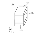
- FIG. 6 is an external perspective view of an electronic component 10c according to another embodiment.
- FIG. 7 is an exploded perspective view of the multilayer body 12c of the electronic component 10c.
- the stacking direction of the electronic component 10c is defined as the z-axis direction
- the direction along the side of the electronic component 10c is defined as the x-axis direction
- the direction orthogonal to the x-axis direction and the z-axis direction is defined as the y-axis direction.
- the electronic component 10 c has external electrodes 13 a and 13 b on the upper and lower surfaces of the multilayer body 12 c located at both ends in the z-axis direction. Further, as shown in FIG. 7, the electronic component 10c does not have the lead conductors 16a and 16b. Instead, via hole conductors b21 to b23, b27 to b29 and connection conductors 19a to 19f are provided.
- the via-hole conductors b21 to b23 are provided so as to overlap with the point B when viewed in plan from the z-axis direction and penetrate the magnetic layers 14m to 14o in the z-axis direction.
- the via-hole conductors b21 to b23 are connected to the coil conductor 18e at the point B, and electrically connect the coil conductor 18e and the external electrode 13a.
- the via-hole conductors b27 to b29 are provided so as to overlap with the point B when viewed in plan from the z-axis direction and penetrate the magnetic layers 14s to 14u in the z-axis direction. As a result, the via-hole conductors b27 to b29 are connected to the coil conductor 18g at the point B via the via-hole conductor b26, and electrically connect the coil conductor 18g and the external electrode 13b.
- connection conductors 19a to 19f are provided so as to overlap with the via-hole conductors b21 to b23 and b27 to b29 in the magnetic layers 14m to 14o and 14s to 14u, respectively. Since the end of the coil conductor 18e is left, the via-hole conductor b23 and the coil conductor 18e will not be disconnected even if the magnetic layer 14o is displaced in the positive direction of the y-axis during lamination.
- the coil L may be electrically connected to the external electrodes 13a and 13b via the via-hole conductors b21 to b23 and b27 to b29.
- the via-hole conductor b23 is provided so as to overlap any of the points A to D, the length of the coil L can be adjusted without changing the positions of the via-hole conductors b21 to b23. .
- the magnetic layers 14l, 14k, 14j, 14i, 14h, 14g, 14f, 14e, 14d, 14c, 14b, and 14a are stacked in this order from the lower side to the upper side.
- the stacking order of the magnetic layers 14 is not limited to this.
- the magnetic layers 14a to 14l may be stacked in this order.
- the magnetic layer 14 is laminated so that the main surface on which the coil conductor 18 is provided faces downward.
- the magnetic layer 14d is disposed below the magnetic layers 14e to 14l in the stacking direction.
- the present invention is useful for an electronic component and a method for manufacturing the same, and is particularly excellent in that it is not necessary to change the shape of the lead conductor or the position of the via hole conductor when changing the number of turns of the coil.
Landscapes
- Engineering & Computer Science (AREA)
- Power Engineering (AREA)
- Microelectronics & Electronic Packaging (AREA)
- Coils Or Transformers For Communication (AREA)
- Manufacturing Cores, Coils, And Magnets (AREA)
Abstract
Description
図1は、電子部品10a,10bの外観斜視図である。図2及び図4は、電子部品10aの積層体12aの分解斜視図である。図3は、参考例に係る電子部品10a'の積層体12a'の分解斜視図である。以下、電子部品10aの積層方向をz軸方向と定義し、電子部品10aの長辺に沿った方向をx軸方向と定義し、電子部品10aの短辺に沿った方向をy軸方向と定義する。
以下に、電子部品10aの製造方法について図1及び図2を参照しながら説明する。
以上のような電子部品10a及びその製造方法によれば、以下に説明するように、引き出し導体16aの形状及びビアホール導体b1の位置を変更することなく、コイルLのターン数を変更することができる。より詳細には、コイルLのターン数を増減させる場合には、磁性体層14dのz軸方向の負方向側にコイル導体18が設けられた磁性体層14を追加することにより、コイルLのターン数を増加させることができる。また、磁性体層14dのz軸方向の負方向側に位置する磁性体層14を取り除くことにより、コイルLのターン数を減少させることができる。以下に、コイルLのターン数を減少させる場合を例にとって説明する。
以下に、電子部品10aの変形例について図面を参照しながら説明する。図5は、変形例に係る電子部品10bの積層体12bの分解斜視図である。
本発明に係る電子部品は、前記実施形態に示した電子部品10a,10bに限らず、その要旨の範囲内において変更可能である。
L コイル
b1~b5,b21~b29 ビアホール導体
10a,10b,10c 電子部品
12a~12c 積層体
13a,13b 外部電極
14a~14u 磁性体層
16a,16b 引き出し導体
18a~18g コイル導体
19a~19f 接続導体
Claims (8)
- 複数の絶縁体層が積層されてなる積層体と、
前記積層体内に内蔵されている螺旋状のコイルと、
前記積層体の表面に設けられている外部電極と、
を備え、
前記コイルは、
前記絶縁体層の積層方向の上側の主面に設けられているコイル導体であって、積層方向から平面視したときに、該絶縁体層上の特定の点において互いに重なっている複数のコイル導体と、
前記絶縁体層に設けられている第1のビアホール導体であって、積層方向から平面視したときに、前記特定の点において前記複数のコイル導体と重なっていると共に、前記外部電極と電気的に接続されている第1のビアホール導体と、
を含み、
前記第1のビアホール導体が設けられている前記絶縁体層は、前記コイル導体が設けられている前記複数の絶縁体層よりも、積層方向の上側に設けられ、
前記第1のビアホール導体は、積層方向から平面視したときに、前記コイル導体の端部以外の位置において、該コイル導体に接続されていること、
を特徴とする電子部品。 - 前記コイルは、
前記絶縁体層の積層方向の上側の主面に設けられている内部導体であって、前記第1のビアホール導体及び前記外部電極に接続されている内部導体を、
更に含んでいること、
を特徴とする請求項1に記載の電子部品。 - 前記複数のコイル導体は、互いに重なり合って、環状の軌道を形成し、
前記内部導体は、前記環状の軌道に重なっていること、
を特徴とする請求項2に記載の電子部品。 - 前記複数のコイル導体は、nを自然数としたときに、(n/n+1)ターンのターン数を有していると共に、端部に位置する前記特定の点において、積層方向に隣り合う前記コイル導体と重なっており、
前記コイルは、
前記特定の点において、積層方向に隣り合う前記コイル導体を接続する複数の第2のビアホール導体を、
更に含んでいること、
を特徴とする請求項1ないし請求項3のいずれかに記載の電子部品。 - 螺旋状のコイルを内蔵する積層体及び該積層体の表面に設けられた外部電極により構成される電子部品の製造方法において、
複数の絶縁体層を準備する工程と、
積層方向から平面視したときに、前記複数の絶縁体層上の特定の点と重なるコイル導体を、該複数の絶縁体層に形成する工程と、
前記外部電極に電気的に接続される第1のビアホール導体であって、積層方向から平面視したときに、前記特定の点と重なる第1のビアホール導体を、前記絶縁体層に形成する工程と、
前記コイルが所望のターン数を有するように前記コイル導体が形成された前記複数の絶縁体層の枚数を調整して、該複数の絶縁体層を積層すると共に、該コイル導体が形成された該複数の絶縁体層よりも積層方向の上側又は下側に、前記第1のビアホール導体が形成された前記絶縁体層を積層する工程と、
前記外部電極を形成する工程と、
を備えていること、
を特徴とする電子部品の製造方法。 - 前記コイル導体が形成される前記複数の絶縁体層の前記特定の点に、積層方向に隣り合う前記コイル導体同士を接続する複数の第2のビアホール導体を形成する工程を、
更に備え、
前記コイル導体を形成する工程では、nを自然数としたときに、(n/n+1)ターンのターン数を有すると共に、端部に位置する前記特定の点において、積層方向に隣り合う前記コイル導体同士が重なるように、前記コイル導体を形成すること、
を特徴とする請求項5に記載の電子部品の製造方法。 - 前記第1のビアホール導体が形成された前記絶縁体層に、該第1のビアホール導体及び前記外部電極に接続される内部導体を形成する工程を、
更に備えていること、
を特徴とする請求項5又は請求項6のいずれかに記載の電子部品の製造方法。 - 前記コイル導体を形成する工程では、前記複数のコイル導体が互いに重なり合って環状の軌道を形成するように、該複数のコイル導体を形成し、
前記内部導体を形成する工程では、前記環状の軌道に重なるように該内部導体を形成すること、
を特徴とする請求項7に記載の電子部品の製造方法。
Priority Applications (2)
| Application Number | Priority Date | Filing Date | Title |
|---|---|---|---|
| JP2011505908A JP5365689B2 (ja) | 2009-03-26 | 2010-01-21 | 電子部品及びその製造方法 |
| CN201080012972.2A CN102362320B (zh) | 2009-03-26 | 2010-01-21 | 电子部件及其制造方法 |
Applications Claiming Priority (2)
| Application Number | Priority Date | Filing Date | Title |
|---|---|---|---|
| JP2009-077123 | 2009-03-26 | ||
| JP2009077123 | 2009-03-26 |
Publications (1)
| Publication Number | Publication Date |
|---|---|
| WO2010109936A1 true WO2010109936A1 (ja) | 2010-09-30 |
Family
ID=42780633
Family Applications (1)
| Application Number | Title | Priority Date | Filing Date |
|---|---|---|---|
| PCT/JP2010/050718 Ceased WO2010109936A1 (ja) | 2009-03-26 | 2010-01-21 | 電子部品及びその製造方法 |
Country Status (3)
| Country | Link |
|---|---|
| JP (1) | JP5365689B2 (ja) |
| CN (1) | CN102362320B (ja) |
| WO (1) | WO2010109936A1 (ja) |
Cited By (3)
| Publication number | Priority date | Publication date | Assignee | Title |
|---|---|---|---|---|
| JP2016139742A (ja) * | 2015-01-28 | 2016-08-04 | 株式会社村田製作所 | コイル部品 |
| CN107968247A (zh) * | 2017-11-28 | 2018-04-27 | 上海坤锐电子科技有限公司 | 一种天线结构、阅读器和智能售货设备 |
| JP2025002251A (ja) * | 2023-06-22 | 2025-01-09 | 株式会社村田製作所 | インダクタ部品 |
Families Citing this family (2)
| Publication number | Priority date | Publication date | Assignee | Title |
|---|---|---|---|---|
| CN105098300A (zh) * | 2015-09-11 | 2015-11-25 | 禾邦电子(中国)有限公司 | 共模滤波器及其制造方法 |
| JP6459946B2 (ja) * | 2015-12-14 | 2019-01-30 | 株式会社村田製作所 | 電子部品及びその製造方法 |
Citations (3)
| Publication number | Priority date | Publication date | Assignee | Title |
|---|---|---|---|---|
| JPH0354808A (ja) * | 1989-07-21 | 1991-03-08 | Murata Mfg Co Ltd | 積層型インダクタンス部品 |
| JPH11317308A (ja) * | 1998-05-01 | 1999-11-16 | Taiyo Yuden Co Ltd | 積層インダクタ及びその製造方法 |
| JP2005167130A (ja) * | 2003-12-05 | 2005-06-23 | Murata Mfg Co Ltd | 積層型電子部品の製造方法および積層型電子部品 |
Family Cites Families (2)
| Publication number | Priority date | Publication date | Assignee | Title |
|---|---|---|---|---|
| JP3438859B2 (ja) * | 1996-11-21 | 2003-08-18 | ティーディーケイ株式会社 | 積層型電子部品とその製造方法 |
| JP4973996B2 (ja) * | 2007-08-10 | 2012-07-11 | 日立金属株式会社 | 積層電子部品 |
-
2010
- 2010-01-21 CN CN201080012972.2A patent/CN102362320B/zh active Active
- 2010-01-21 WO PCT/JP2010/050718 patent/WO2010109936A1/ja not_active Ceased
- 2010-01-21 JP JP2011505908A patent/JP5365689B2/ja active Active
Patent Citations (3)
| Publication number | Priority date | Publication date | Assignee | Title |
|---|---|---|---|---|
| JPH0354808A (ja) * | 1989-07-21 | 1991-03-08 | Murata Mfg Co Ltd | 積層型インダクタンス部品 |
| JPH11317308A (ja) * | 1998-05-01 | 1999-11-16 | Taiyo Yuden Co Ltd | 積層インダクタ及びその製造方法 |
| JP2005167130A (ja) * | 2003-12-05 | 2005-06-23 | Murata Mfg Co Ltd | 積層型電子部品の製造方法および積層型電子部品 |
Cited By (4)
| Publication number | Priority date | Publication date | Assignee | Title |
|---|---|---|---|---|
| JP2016139742A (ja) * | 2015-01-28 | 2016-08-04 | 株式会社村田製作所 | コイル部品 |
| CN107968247A (zh) * | 2017-11-28 | 2018-04-27 | 上海坤锐电子科技有限公司 | 一种天线结构、阅读器和智能售货设备 |
| CN107968247B (zh) * | 2017-11-28 | 2020-01-10 | 上海坤锐电子科技有限公司 | 一种天线结构、阅读器和智能售货设备 |
| JP2025002251A (ja) * | 2023-06-22 | 2025-01-09 | 株式会社村田製作所 | インダクタ部品 |
Also Published As
| Publication number | Publication date |
|---|---|
| CN102362320B (zh) | 2014-07-30 |
| CN102362320A (zh) | 2012-02-22 |
| JPWO2010109936A1 (ja) | 2012-09-27 |
| JP5365689B2 (ja) | 2013-12-11 |
Similar Documents
| Publication | Publication Date | Title |
|---|---|---|
| JP5533673B2 (ja) | 電子部品 | |
| JP5994933B2 (ja) | 電子部品 | |
| JP5900373B2 (ja) | 電子部品 | |
| JP5598452B2 (ja) | 電子部品及びその製造方法 | |
| JP5029761B2 (ja) | 積層インダクタ | |
| JP5365689B2 (ja) | 電子部品及びその製造方法 | |
| JP2010263059A (ja) | 電子部品及びその製造方法 | |
| JP5585453B2 (ja) | 積層インダクタ | |
| JP2014078650A (ja) | 電子部品及びその製造方法 | |
| WO2011145517A1 (ja) | 電子部品 | |
| JP2011192737A (ja) | 電子部品及びその製造方法 | |
| JP5327231B2 (ja) | 電子部品 | |
| JP5262813B2 (ja) | 電子部品及びその製造方法 | |
| CN101884076A (zh) | 叠层型电子部件 | |
| WO2010010799A1 (ja) | 電子部品及びその製造方法 | |
| WO2014181756A1 (ja) | 電子部品 | |
| WO2009147899A1 (ja) | 電子部品及びその製造方法 | |
| JP2011091221A (ja) | 電子部品 | |
| JP2010147416A (ja) | 電子部品 | |
| JP2010034175A (ja) | 電子部品及びその製造方法 | |
| JP2013153100A (ja) | 電子部品 | |
| JP2010161161A (ja) | 積層インダクタ | |
| WO2010061679A1 (ja) | 電子部品 |
Legal Events
| Date | Code | Title | Description |
|---|---|---|---|
| WWE | Wipo information: entry into national phase |
Ref document number: 201080012972.2 Country of ref document: CN |
|
| 121 | Ep: the epo has been informed by wipo that ep was designated in this application |
Ref document number: 10755737 Country of ref document: EP Kind code of ref document: A1 |
|
| WWE | Wipo information: entry into national phase |
Ref document number: 2011505908 Country of ref document: JP |
|
| NENP | Non-entry into the national phase |
Ref country code: DE |
|
| 122 | Ep: pct application non-entry in european phase |
Ref document number: 10755737 Country of ref document: EP Kind code of ref document: A1 |