WO2010109853A1 - シリコンウェーハおよびその製造方法 - Google Patents
シリコンウェーハおよびその製造方法 Download PDFInfo
- Publication number
- WO2010109853A1 WO2010109853A1 PCT/JP2010/002060 JP2010002060W WO2010109853A1 WO 2010109853 A1 WO2010109853 A1 WO 2010109853A1 JP 2010002060 W JP2010002060 W JP 2010002060W WO 2010109853 A1 WO2010109853 A1 WO 2010109853A1
- Authority
- WO
- WIPO (PCT)
- Prior art keywords
- wafer
- silicon wafer
- heat treatment
- silicon
- stress
- Prior art date
- Legal status (The legal status is an assumption and is not a legal conclusion. Google has not performed a legal analysis and makes no representation as to the accuracy of the status listed.)
- Ceased
Links
Images



Classifications
-
- C—CHEMISTRY; METALLURGY
- C30—CRYSTAL GROWTH
- C30B—SINGLE-CRYSTAL GROWTH; UNIDIRECTIONAL SOLIDIFICATION OF EUTECTIC MATERIAL OR UNIDIRECTIONAL DEMIXING OF EUTECTOID MATERIAL; REFINING BY ZONE-MELTING OF MATERIAL; PRODUCTION OF A HOMOGENEOUS POLYCRYSTALLINE MATERIAL WITH DEFINED STRUCTURE; SINGLE CRYSTALS OR HOMOGENEOUS POLYCRYSTALLINE MATERIAL WITH DEFINED STRUCTURE; AFTER-TREATMENT OF SINGLE CRYSTALS OR A HOMOGENEOUS POLYCRYSTALLINE MATERIAL WITH DEFINED STRUCTURE; APPARATUS THEREFOR
- C30B29/00—Single crystals or homogeneous polycrystalline material with defined structure characterised by the material or by their shape
- C30B29/02—Elements
- C30B29/06—Silicon
-
- C—CHEMISTRY; METALLURGY
- C30—CRYSTAL GROWTH
- C30B—SINGLE-CRYSTAL GROWTH; UNIDIRECTIONAL SOLIDIFICATION OF EUTECTIC MATERIAL OR UNIDIRECTIONAL DEMIXING OF EUTECTOID MATERIAL; REFINING BY ZONE-MELTING OF MATERIAL; PRODUCTION OF A HOMOGENEOUS POLYCRYSTALLINE MATERIAL WITH DEFINED STRUCTURE; SINGLE CRYSTALS OR HOMOGENEOUS POLYCRYSTALLINE MATERIAL WITH DEFINED STRUCTURE; AFTER-TREATMENT OF SINGLE CRYSTALS OR A HOMOGENEOUS POLYCRYSTALLINE MATERIAL WITH DEFINED STRUCTURE; APPARATUS THEREFOR
- C30B33/00—After-treatment of single crystals or homogeneous polycrystalline material with defined structure
- C30B33/02—Heat treatment
-
- H—ELECTRICITY
- H10—SEMICONDUCTOR DEVICES; ELECTRIC SOLID-STATE DEVICES NOT OTHERWISE PROVIDED FOR
- H10D—INORGANIC ELECTRIC SEMICONDUCTOR DEVICES
- H10D62/00—Semiconductor bodies, or regions thereof, of devices having potential barriers
- H10D62/60—Impurity distributions or concentrations
-
- H—ELECTRICITY
- H10—SEMICONDUCTOR DEVICES; ELECTRIC SOLID-STATE DEVICES NOT OTHERWISE PROVIDED FOR
- H10P—GENERIC PROCESSES OR APPARATUS FOR THE MANUFACTURE OR TREATMENT OF DEVICES COVERED BY CLASS H10
- H10P30/00—Ion implantation into wafers, substrates or parts of devices
- H10P30/20—Ion implantation into wafers, substrates or parts of devices into semiconductor materials, e.g. for doping
-
- H—ELECTRICITY
- H10—SEMICONDUCTOR DEVICES; ELECTRIC SOLID-STATE DEVICES NOT OTHERWISE PROVIDED FOR
- H10P—GENERIC PROCESSES OR APPARATUS FOR THE MANUFACTURE OR TREATMENT OF DEVICES COVERED BY CLASS H10
- H10P95/00—Generic processes or apparatus for manufacture or treatments not covered by the other groups of this subclass
- H10P95/90—Thermal treatments, e.g. annealing or sintering
-
- H—ELECTRICITY
- H10—SEMICONDUCTOR DEVICES; ELECTRIC SOLID-STATE DEVICES NOT OTHERWISE PROVIDED FOR
- H10D—INORGANIC ELECTRIC SEMICONDUCTOR DEVICES
- H10D30/00—Field-effect transistors [FET]
- H10D30/60—Insulated-gate field-effect transistors [IGFET]
- H10D30/601—Insulated-gate field-effect transistors [IGFET] having lightly-doped drain or source extensions, e.g. LDD IGFETs or DDD IGFETs
Definitions
- the present invention relates to a silicon wafer and a method for manufacturing the same, and more particularly to a technique suitable for use in a silicon wafer subjected to a heat treatment that generates a high internal stress.
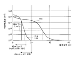
- an annealing process called FLA (Flash Lamp Annealing), LSA (Laser Spike Annealing), or LTP (Laser Thermal Process) may be used from the 45 nm node (hp65).
- FLA heat treatment the wafer is heated to an initial temperature of 400 ° C. to 600 ° C., and the entire surface of the wafer is irradiated with light having a short wavelength, such as an Xe lamp. Rapidly heat up to the vicinity and then cool down.
- the heat treatment time is a unit (order) of ⁇ seconds to milliseconds.
- Such a heat treatment causes a temperature difference of several hundred degrees Celsius between the front and back surfaces of the wafer, and a very high stress is applied as compared with RTA (Rapid Thermal Annealing) that has been performed previously.
- RTA Rapid Thermal Annealing
- the present invention has been made in view of the above circumstances, and an object thereof is to provide a wafer having crack resistance even in the millisecond annealing by the FLA annealing treatment.
- the inventors have a high processing temperature (peak temperature) in FLA and LSA, and since the temperature is raised and lowered in a very short time, the stress applied to the wafer increases and the wafer is cracked. We sought a means to provide a wafer that could withstand this.
- peak temperature peak temperature
- preventing cracks by preventing slip elongation due to oxygen precipitates in the wafer which has been adopted as a means for preventing cracks during RTA, is almost ineffective because the temperature conditions in the above heat treatment are too severe and severe. It was.
- crack prevention measures corresponding to these heating methods are necessary. Therefore, in order to prevent the wafer from cracking in the heat treatment under such conditions, the relationship between the presence or absence of scratches (cracks) on the wafer surface and the occurrence of cracking was investigated.
- the method for producing a silicon wafer of the present invention is a method for producing a silicon wafer, A wafer preparation step of slicing a silicon single crystal ingot and surface-treating the sliced silicon wafer; A stress setting step for setting a stress S (MPa) applied to the silicon wafer prepared in the wafer preparation step; An inspection process for inspecting scratches present on the front surface or the back surface of the silicon wafer; A determination process for determining whether or not the silicon wafer inspected in the inspection process satisfies the criterion of the following formula (A), a silicon wafer that satisfies the criterion is accepted, and a silicon wafer that does not satisfy the criterion is rejected and stress S ⁇ Scratch size C ⁇ 3500 (MPa ⁇ ⁇ m) (A) C: Size of the scratch ( ⁇ m) existing on the front or back surface of the silicon wafer Is provided.
- the processing conditions in the heat treatment may be a processing temperature of 1100 ° C. or higher and a melting point of silicon or lower and a processing time of about 1 ⁇ sec to 100 msec.
- the silicon wafer manufacturing method when it is found that the number of LPDs having a size of 2 ⁇ m or more on the back surface of the silicon wafer in the inspection step is 10 or less, the silicon wafer is determined in the determination step as a reference of the above (A). You may determine with satisfy
- a silicon wafer that is determined not to satisfy the criterion (A) in the determination step may be surface-treated again in the wafer preparation step.
- the oxygen concentration Oi of the silicon wafer may be set to 5 ⁇ 10 17 to 20 ⁇ 10 17 atoms / cm 3 (Old-ASTM).
- the silicon wafer of the present invention can be manufactured by the silicon wafer manufacturing method.
- the silicon wafer of the present invention is mirror-finished and used for a semiconductor device manufacturing process having a heat treatment step under conditions where the maximum temperature is 1100 ° C. or higher and below the melting point of silicon and the processing time is about 1 ⁇ sec to 100 msec.
- the stress generated at each point of the silicon wafer by the heat treatment is S (MPa) and the size of the scratch existing on the back surface of the silicon wafer is C ( ⁇ m)
- the size of the scratch may be set so as to satisfy.
- the number of LPDs having a size of 2 ⁇ m or more on the back surface of the silicon wafer is more preferably 10 or less.
- the oxygen concentration Oi of the silicon wafer may be within a range of 5 ⁇ 10 17 to 20 ⁇ 10 17 atoms / cm 3 (Old-ASTM).
- the silicon wafer manufacturing method of the present invention includes a heat treatment step in which after the silicon wafer is mirror-finished, the maximum temperature is 1100 ° C. or more and the melting point of silicon or less and the treatment time is set to about 1 ⁇ sec to 100 msec.
- a method for manufacturing a silicon wafer used in a semiconductor device manufacturing process When the stress generated at each point of the silicon wafer by the heat treatment is S (MPa) and the size of the scratch existing on the back surface of the silicon wafer is C ( ⁇ m), the following formula (A) Stress S ⁇ Scratch size C ⁇ 3500 (MPa ⁇ ⁇ m) (A) The size of the scratch can be set so as to satisfy.
- a means in which the number of LPDs having a size of 2 ⁇ m or more on the back surface of the silicon wafer is 10 or less may be employed.
- the silicon wafer of the present invention is mirror-finished and used for a semiconductor device manufacturing process having a heat treatment step under conditions where the maximum temperature is 1100 ° C. or higher and below the melting point of silicon and the processing time is about 1 ⁇ sec to 100 msec.
- the annealing process of the MOS FET is performed at a higher temperature and in a shorter time than the conventional RTA.
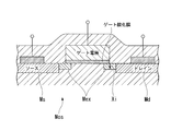
- this is an ultra-shallow junction which is a shallow impurity diffusion region having a depth (junction depth) Xi of about 20 nm adjacent to the source Ms and drain Md of the MOS FET indicated by the symbol Mos.
- This is because, in Mex, it is necessary to realize a box-shaped impurity profile as shown in FIG. 4, that is, a uniform impurity concentration in the ultra-shallow junction Mex region and a steep change state at the boundary.
- the impurities implanted by the high heating temperature are sufficiently activated to lower the resistance, and at the same time, unnecessary diffusion of the impurities is suppressed by a short heating time and the deactivation of the activated impurities is avoided. is there.
- the wafer is heated to an initial temperature of 400 ° C. to 600 ° C. or less, and a short such as a Xe flash lamp is used.
- FLA that irradiates the entire surface of the wafer with light of a wavelength and rapidly heats and cools only the surface of the wafer electrode to about 900 ° C. to 1350 ° C. with a heat treatment time in milliseconds, or 400 ° C. to 600 ° C. on the hot plate.
- the wafer is spot-scanned by irradiating with a continuous wave laser, rapidly heated to 1100 ° C.
- LSA etc. are performed.
- the impurity concentration distribution characteristic of the ultra-shallow junction region indicated by Mex in FIG. 3 is maintained, junction leakage is reduced, gate leakage is suppressed, source / drain parasitic resistance is reduced, and gate depletion is also suppressed.
- a feasible processing condition is selected.
- the internal stress generated in the wafer during the heat treatment is at a level of 50 to 150 MPa. Reach.
- the temperature difference that occurs in the LSA also occurs around the laser spot to be irradiated in addition to the wafer thickness direction, that is, in the wafer in-plane direction, whereas in the FLA that uniformly heats in the wafer in-plane direction. Is mainly in the wafer thickness direction, it is considered that the internal stress generated in the wafer during the heat treatment is smaller than that in the case of FLA as compared with LSA.
- the number of LPDs having a size of 2 ⁇ m or more on the back surface of the silicon wafer is 10 or less, a wafer satisfying the above-described formula (A) can be manufactured.
- a wafer back surface state capable of preventing the occurrence of cracking required in accordance with the rapid heating / cooling heat treatment step that is the FLA in the manufacturing process of the semiconductor device that provides the silicon wafer.
- a laser microscope or dark field microscope using a confocal optical system is a method in which a laser beam is focused on a sample and irradiated with a minute spot, and the reflected light is focused again on a pinhole arranged on the entire surface of the light receiver. It detects the amount of light that has passed, and specifically, it is possible to employ Magics manufactured by Lasertec Corporation.
- the oxygen concentration Oi of the silicon wafer can be in the range of 5 ⁇ 10 17 to 20 ⁇ 10 17 atoms / cm 3 (Old-ASTM).
- the silicon wafer manufacturing method of the present invention includes a semiconductor device having a heat treatment step under conditions in which the maximum temperature is 1100 ° C. or more and the melting point of silicon or less and the processing time is about 1 ⁇ sec to 100 msec after mirror-finishing the silicon wafer.
- the FLA in the manufacturing process of a semiconductor device that provides a silicon wafer is adopted by adopting a means in which the number of LPDs having a size of 2 ⁇ m or more on the back surface of the silicon wafer is 10 or less. It is possible to realize a wafer back surface state capable of preventing the occurrence of cracks required according to the rapid heating / cooling heat treatment process.
- the method for producing a silicon wafer of the present invention is a method for producing a silicon wafer, A wafer preparation step of slicing a silicon single crystal ingot and surface-treating the sliced silicon wafer; A stress setting step for setting a stress S (MPa) applied to the silicon wafer prepared in the wafer preparation step; An inspection process for inspecting scratches present on the front surface or the back surface of the silicon wafer; A determination process for determining whether or not the silicon wafer inspected in the inspection process satisfies the criterion of the following formula (A), a silicon wafer that satisfies the criterion is accepted, and a silicon wafer that does not satisfy the criterion is rejected and stress S ⁇ Scratch size C ⁇ 3500 (MPa ⁇ ⁇ m) (A) C: Size of the scratch ( ⁇ m) existing on the front or back surface of the silicon wafer It is possible to prevent the occurrence of cracks required according to the FLA heat treatment process in the semiconductor device manufacturing process by judging pass
- the implanted impurity is electrically activated and a heat treatment that can remove the crystal defects caused by the impurity implantation is performed. This makes it possible to manufacture a silicon wafer that does not cause cracking of the wafer under conditions that can realize a state close to a so-called rectangular impurity profile.
- the processing conditions in the heat treatment are as follows: the processing temperature is set to 1100 ° C. or higher and the melting point of silicon and the processing time is set to 1 ⁇ sec to 100 msec, thereby maintaining the electrical activation of the impurities and the rectangular impurity profile. In this state, it is possible to prevent the occurrence of cracks even in a FLA where there is a high possibility of cracks due to scratches present in the center of the wafer.
- the number of LPDs having a size of 2 ⁇ m or more on the back surface of a silicon wafer in the inspection process is 10 or less, it is determined that the silicon wafer satisfies the criterion (A) in the determination process. Thus, it becomes possible to discriminate the wafer capable of preventing the crack.
- the silicon wafer that has been rejected in the determination step is surface-treated again in the wafer preparation step, so that the determination step can be accepted again.
- the reprocessing in the wafer preparation process is a back surface polishing process, and this polishing process is a so-called finish polishing, and has a polishing process in which the polishing allowance of the silicon wafer back surface is 1 ⁇ m or more and 3 ⁇ m or less. Even if a flaw is introduced during the wafer preparation process (silicon wafer manufacturing process), it is possible to remove the flaw and eliminate its influence, thereby preventing the wafer from cracking in the FLA process. It becomes.
- the oxygen concentration Oi of the silicon wafer can be set within a range of 5 ⁇ 10 17 to 20 ⁇ 10 17 atoms / cm 3 (Old-ASTM).
- the silicon wafer of the present invention can be manufactured by the above-described silicon wafer manufacturing method.
- a silicon wafer capable of preventing the generation of cracks from the center of the wafer in the manufacturing process of a semiconductor device having a heat treatment process such as FLA in which an extremely large stress is generated compared to RTA.
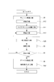
- FIG. 1 is a flowchart showing a method for manufacturing a silicon wafer in the present embodiment.
- the maximum temperature is 1100 ° C. or more and the melting point of silicon
- the processing time is 1 ⁇ sec to 100 msec, or 1 ⁇ sec to 10 msec.
- a silicon single crystal is pulled up from a silicon melt by a CZ (Czochralski) method, the silicon single crystal is sliced, and surface treatment such as chamfering, grinding, polishing, and cleaning is performed.
- surface treatment such as chamfering, grinding, polishing, and cleaning is performed.
- the step includes a polishing step S12 as a finish.
- the oxygen concentration Oi of the silicon wafer is set to 5 ⁇ 10 17 to 20 ⁇ 10 17 atoms / cm 3 (Old-ASTM).
- the stress setting step S2 shown in FIG. 1 is generated in the wafer surface layer in accordance with the rapid heating / cooling heat treatment step S52 such as FLA in the semiconductor device manufacturing step S5 as a post-process for providing the silicon wafer prepared in the wafer preparation step S1.
- the specific condition of the heat treatment condition is that the heat treatment for which a mirror-finished silicon wafer is provided has a maximum temperature of 1100 ° C. or higher.
- a rapid heating / cooling heat treatment step S52 having a temperature below the melting point and a treatment time of about 1 ⁇ sec to about 100 msec is set, and in this heat treatment step S52, the state of the central portion of the wafer back surface capable of suppressing the occurrence of cracks is set.
- the condition of the back surface of the wafer is such that flaws of 10 ⁇ m or more that cause silicon wafer cracking in the heat treatment step S52 are eliminated by the conditions described later in the wafer central portion Wc shown in FIG.
- the wafer central portion Wc is a region of a distance r that is outward in the wafer radial direction from the center outermost peripheral portion Wo on the back surface Wr of the silicon wafer W.
- the ratio with respect to the wafer radius dimension indicated by R is set within a range of 0 to 2/3.
- a silicon wafer having a diameter of about 300 mm to about 450 mm can be applied.
- the target heat treatment process S52 is to electrically activate the implanted impurity in the annealing process after implanting the impurity into the source / drain diffusion region Mex shown in FIG. And removing the crystal defects caused by the implantation of impurities are performed at the same time.
- the electrical activation means a low electrical conductivity that is electrically inactive only when impurities implanted by ion implantation are usually randomly present in the Si crystal.
- the removal of crystal defects caused by the implantation of impurities means that, as shown in FIG. 5 (a), when the impurities are implanted, the single crystal silicon in which Si atoms are originally regularly arranged is implanted.
- the activation of the former impurity requires only a short movement distance and a short distance between the atoms (interstitial) until the impurity reaches the Si lattice point, and the activation time can be short, but the peak temperature is A high temperature exceeding 1000 ° C. is required. That is, it has a small time constant at a high temperature.
- the latter Si single crystal alignment has a large time constant. This is because the distance that the atoms whose order is broken is moved until they are rearranged is long, and it takes a long time to recrystallize. Therefore, low temperature and long time annealing is required to remove crystal defects. .
- the heat treatment step S52 which is a heat treatment for simultaneously controlling phenomena having different time constants, has severe conditions, and when the heating conditions are set to a high temperature in preference to impurity activation, impurity diffusion is minimized. In order to suppress it, it is necessary to shorten the processing time, but as a result, the crystal defects are not sufficiently removed, and the leakage current of the MOS FET increases. On the other hand, when the treatment time is lengthened by giving priority to the removal of crystal defects, the defects are recovered and the crystallinity is recovered, but the impurity diffusion becomes intense and the short channel effect is likely to be caused.
- the heat treatment step S52 simultaneously fulfills these two conflicting roles and controls two thermal phenomena having different time constants in order to form an extremely shallow junction Mex having a high impurity density and a shallow diffusion depth. Therefore, under such conditions, the frequency of occurrence of wafer cracking is extremely higher than that of conventional RTA, and it is necessary to set the wafer state corresponding to this heat treatment condition.
- the back surface stress state in the wafer stress setting step S2 is a processing condition in which the processing temperature (peak temperature) is 1100 ° C. or higher and the melting point of silicon or lower and the processing time is about 1 ⁇ sec to 100 msec as in an example described later.
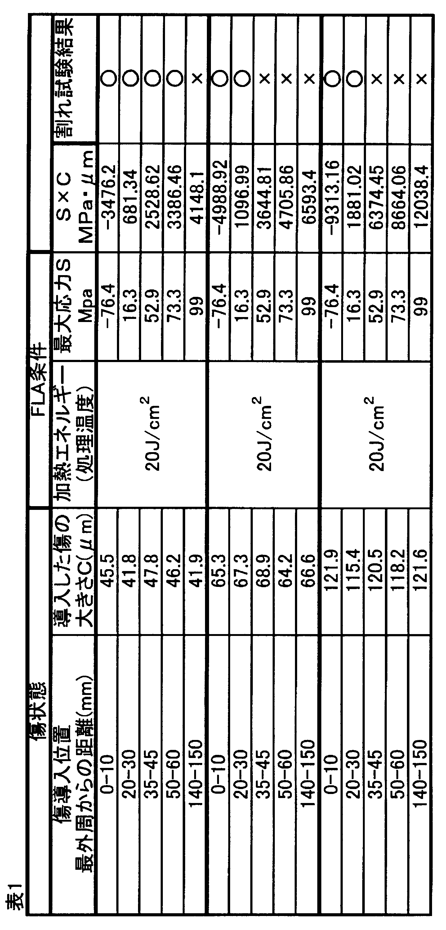
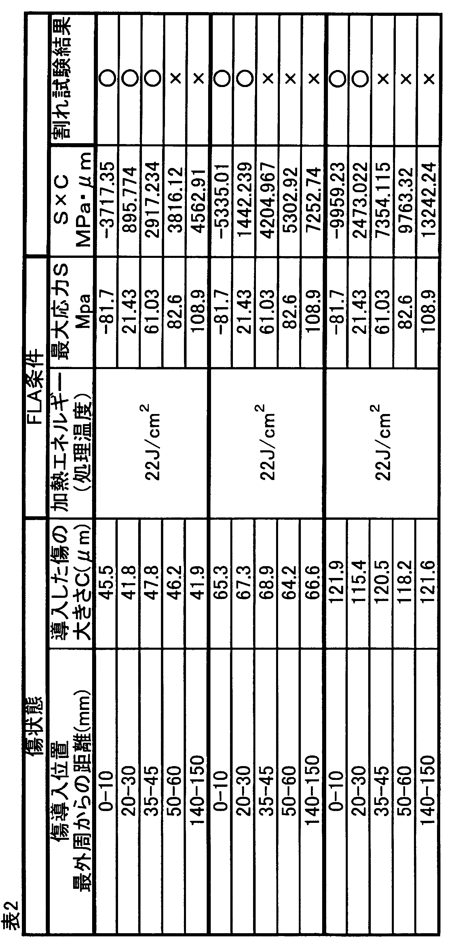
- a scratch of about 40 to 50 ⁇ m has a radial distance from the center.
- scratches of about 60 to 70 ⁇ m are not in the range of 120/300 or less in the radial direction from the center to the radial direction of the wafer
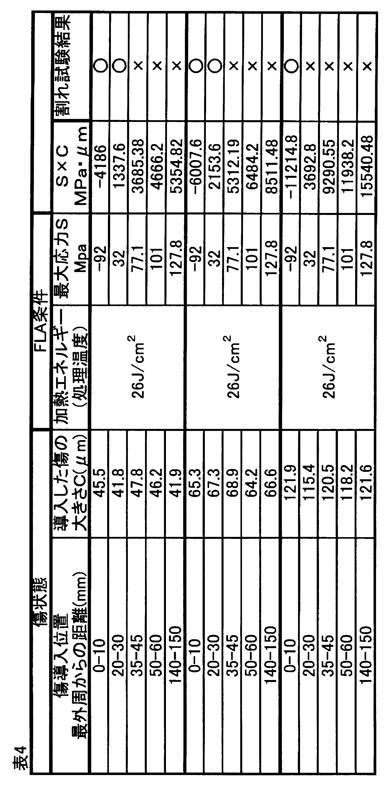
- scratches of about 115 to 125 ⁇ m are the distance from the center to the radial direction of the wafer not within a range of 120/300 to the radial dimension state, corresponding to Table 4, when the heating energy (processing temperature) of 26J / cm 2, scratches on the order of 40 ⁇ 50 [mu] m
- the distance from the center to the radial direction is not within the range of 120/300 with respect to the wafer radial dimension
- the distance from the center to the radial direction of the scratch of about 60 to 70 ⁇ m is within the range of 120/300 with respect to the wafer radial dimension.
- the scratches of about 115 to 125 ⁇ m are set in a state where the distance from the center to the radial direction is not within a range within 130/300 with respect to the wafer radial dimension.
- the wafer surface temperature itself may be about 1050 ° C. and lower than 1100 ° C., but the generated internal stress and the size and presence of scratches Since the relationship itself is not different from the above-described one regardless of the wafer surface temperature state, the heat treatment conditions in which the maximum value of the generated internal stress is greater than 95 MPa even if the temperature state is low are included in the present invention. .
- the maximum value of the generated internal stress can be regarded as occurring in the central portion of the wafer. Further, when the generated stress is a compressive stress, no wafer cracking occurs, so that any stress setting at the wafer edge can be excluded.
- the inspection step S3 shown in FIG. 1 is for inspecting scratches existing on the end surface and the back surface of the silicon wafer, and the ratio of the distance r from the center on the back surface of the silicon wafer to the outside in the wafer radial direction and the wafer diameter size R is 0 to In the range of 2/3 or less, whether or not there are 10 or less LPDs having a size of 2 ⁇ m or more is inspected.
- an inspection method such as an image inspection method using a surface inspection machine (SP-1 manufactured by KLA-Tencor) using a laser or a CCD camera can be used.
- the result of the inspection step S3 is that the ratio of the distance r from the center on the back surface of the silicon wafer toward the outside in the wafer radial direction and the wafer radial dimension R is within 0 to 2/3.
- a wafer that satisfies the criteria that the scratches that satisfy the above-mentioned (A) are eliminated is determined to be acceptable, and a wafer that does not satisfy the above criteria is determined to be unacceptable.
- step S4 If the determination step S4 is rejected, the process returns to the polishing step S12 of the wafer preparation step S1 to remove and recover the scratches on the back and end surfaces of the wafer to the above-mentioned standard, so that the inspection step S3 is determined again. It leads to process S4.
- the silicon wafer is provided to the device manufacturing step S5.
- a necessary process for making a device with a 45 nm node (hp65) into a silicon wafer is performed, and a heat treatment process S52 such as FLA is provided.
- flash lamp annealing is performed by the heat treatment apparatus shown in FIG.
- This FLA apparatus can raise the temperature to about 1350 ° C. by irradiation on the order of microseconds to milliseconds.
- This heat treatment apparatus is an apparatus for performing heat treatment of a substrate such as a silicon wafer by flash light from a xenon flash lamp.
- This heat treatment apparatus includes a translucent plate 61, a bottom plate 62, and a pair of side plates 63 and 64, and includes a chamber 65 for housing a semiconductor wafer (silicon wafer) W and heat-treating it.
- the translucent plate 61 constituting the upper part of the chamber 65 is made of, for example, a material having infrared transparency such as quartz, and functions as a chamber window that transmits light emitted from the light source 5 and guides it into the chamber 65. is doing.
- the bottom plate 62 constituting the chamber 65 is provided with support pins 70 that pass through a susceptor 73 and a heating plate 74 described later to support the semiconductor wafer W from the lower surface thereof.
- an opening 66 for carrying in and out the semiconductor wafer W is formed in the side plate 64 constituting the chamber 65.
- the opening 66 can be opened and closed by a gate valve 68 that rotates about a shaft 67.
- the semiconductor wafer W is loaded into the chamber 65 by a transfer robot (not shown) with the opening 66 released.
- the opening 66 is closed by the gate valve 68.
- the chamber 65 is provided below the light source 5.
- the light source 5 includes a plurality (27 in the present embodiment) of xenon flash lamps 69 (hereinafter also simply referred to as “flash lamps 69”) and a reflector 71.
- the plurality of flash lamps 69 are rod-shaped lamps each having a long cylindrical shape, and are arranged in parallel with each other such that the longitudinal direction thereof is along the horizontal direction.
- the reflector 71 is disposed above the plurality of flash lamps 69 so as to cover them entirely.
- the xenon flash lamp 69 includes a glass tube in which xenon gas is sealed and an anode and a cathode connected to a capacitor at both ends thereof, and a trigger electrode wound around an external portion of the glass tube. Is provided. Since xenon gas is an electrical insulator, electricity does not flow into the glass tube under normal conditions. However, if the insulation is broken by applying a high voltage to the trigger electrode, the electricity stored in the capacitor instantaneously flows into the glass tube, and the xenon gas is heated by Joule heat at that time, and light is emitted. . In the xenon flash lamp 69, the electrostatic energy stored in advance is converted into an extremely short light pulse of 0.1 millisecond to 10 millisecond. It has a feature that
- a light diffusion plate 72 is disposed between the light source 5 and the translucent plate 61.
- a light diffusion plate 72 a surface of quartz glass as an infrared transmitting material subjected to light diffusion processing is used.
- a part of the light emitted from the flash lamp 69 passes directly through the light diffusion plate 72 and the light transmission plate 61 and goes into the chamber 65. Further, another part of the light emitted from the flash lamp 69 is once reflected by the reflector 71, then passes through the light diffusing plate 72 and the light transmitting plate 61 and goes into the chamber 65.
- a heating plate 74 and a susceptor 73 are provided in the chamber 65.
- the susceptor 73 is attached to the upper surface of the heating plate 74.
- the heating plate 74 and the susceptor 73 constitute holding means for holding the semiconductor wafer W in the chamber 65 in a substantially horizontal posture.
- the heating plate 74 is for preheating (assist heating) the semiconductor wafer W.
- the heating plate 74 is made of aluminum nitride and has a configuration in which a heater and a sensor for controlling the heater are housed.
- the susceptor 73 positions and holds the semiconductor wafer W and diffuses the heat energy from the heating plate 74 to uniformly preheat the semiconductor wafer W.
- a material having a relatively low thermal conductivity such as aluminum nitride or quartz is employed. Details of the susceptor 73 will be described later.
- the susceptor 73 and the heating plate 74 are configured to move up and down between the loading / unloading position of the semiconductor wafer W and the heat treatment position of the semiconductor wafer W by driving the motor 40.
- the heating plate 74 is connected to the moving plate 42 via the cylindrical body 41.
- the moving plate 42 can be moved up and down by being guided by a guide member 43 supported by a bottom plate 62 of the chamber 65.
- a fixed plate 44 is fixed to the lower end portion of the guide member 43, and a motor 40 that rotationally drives a ball screw 45 is disposed at the central portion of the fixed plate 44.
- the ball screw 45 is screwed with a nut 48 connected to the moving plate 42 via connecting members 46 and 47. Therefore, the susceptor 73 and the heating plate 74 can move up and down between the loading / unloading position of the semiconductor wafer W and the heat treatment position of the semiconductor wafer W by driving the motor 40.
- the loading / unloading position of the semiconductor wafer W is set such that the semiconductor wafer W loaded from the opening 66 using a transfer robot (not shown) is placed on the support pins 70 or the semiconductor wafer placed on the support pins 70.
- the susceptor 73 and the heating plate 74 are lowered so that W can be carried out of the opening 66.
- the upper end of the support pin 70 passes through a through hole formed in the susceptor 73 and the heating plate 74 and protrudes upward from the surface of the susceptor 73.
- the heat treatment position of the semiconductor wafer W shown in the figure is a position where the susceptor 73 and the heating plate 74 are raised above the upper ends of the support pins 70 in order to perform heat treatment on the semiconductor wafer W.
- the semiconductor wafer W placed on the support pins 70 is received by the susceptor 73 and its lower surface is supported by the surface of the susceptor 73 and lifted. Then, it is held in a horizontal posture at a position in the chamber 65 close to the translucent plate 61.
- the semiconductor wafer W supported by the susceptor 73 is transferred to the support pins 70.
- the translucent plate 61 is positioned between the semiconductor wafer W held by them and the light source 5.
- the distance between the susceptor 73 and the light source 5 at this time can be adjusted to an arbitrary value by controlling the rotation amount of the motor 40.
- a telescopic bellows 77 is disposed so as to surround the cylindrical body 41 so as to maintain the chamber 65 in an airtight state.
- the bellows 77 contracts, and when the susceptor 73 and the heating plate 74 are lowered to the loading / unloading position, the bellows 77 is extended, and the atmosphere in the chamber 65 and the external atmosphere are increased. Cut off.
- an introduction path 78 connected to the on-off valve 80 is formed in the side plate 63 opposite to the opening 66 in the chamber 65.
- the introduction path 78 introduces a gas necessary for processing, for example, an inert nitrogen gas, into the chamber 65.
- a discharge passage 79 connected to the on-off valve 81 is formed in the opening 66 in the side plate 64.
- the discharge path 79 is for discharging the gas in the chamber 65, and is connected to an exhaust means (not shown) via the on-off valve 81.
- a semiconductor wafer W to be processed in this heat treatment apparatus is a semiconductor wafer after ion implantation.
- the semiconductor wafer W is loaded through the opening 66 by a transfer robot (not shown), and the support pins 70. Placed on top.
- the opening 66 is closed by the gate valve 68.
- the susceptor 73 and the heating plate 74 are raised to the heat treatment position of the semiconductor wafer W shown in FIG. 7 by driving the motor 40, and hold the semiconductor wafer W in a horizontal posture.
- the on-off valve 80 and the on-off valve 81 are opened to form a nitrogen gas flow in the chamber 65.
- the susceptor 73 receives the semiconductor wafer W placed on the support pins 70.
- a thin air layer is sandwiched between the susceptor 73 and the semiconductor wafer W for several seconds after the semiconductor wafer W is transferred from the support pins 70 to the susceptor 73, and the semiconductor wafer W is separated from the susceptor 73 by the air layer. Slightly floated.
- the phenomenon that the semiconductor wafer W moves so as to slide in the recess 97 due to some cause (for example, a slight inclination), and the wafer end is rebounded by the tapered surface 95 is repeated for several seconds.
- the air layer is eventually removed, so that the semiconductor wafer W is stably held in the recess 97 of the susceptor 73. That is, the slightly floating semiconductor wafer W is positioned by the taper surface 95 and is held on the lowest position of the recess 97, that is, on the mounting surface 99 without providing a special positioning pin or the like.
- the diameter of the mounting surface 99 is slightly larger than the diameter of the semiconductor wafer W, and the semiconductor wafer W is normally positioned and held eccentrically on the mounting surface 99, so that one point of the peripheral end contacts the tapered surface 95. In a stable state.
- the susceptor 73 and the heating plate 74 are preheated to a predetermined temperature by the action of a heater built in the heating plate 74. For this reason, in a state where the susceptor 73 and the heating plate 74 are raised to the heat treatment position of the semiconductor wafer W, the semiconductor wafer W is preheated by coming into contact with the heated susceptor 73, and the temperature of the semiconductor wafer W gradually increases. To do.
- the semiconductor wafer W is continuously heated by the susceptor 73.
- a temperature sensor (not shown) always monitors whether or not the surface temperature of the semiconductor wafer W has reached the preheating temperature T1.
- the preheating temperature T1 is, for example, about 200 ° C. to 600 ° C. Even if the semiconductor wafer W is heated to such a preheating temperature T1, ions implanted into the semiconductor wafer W do not diffuse.
- the flash lamp 69 is turned on to perform flash heating.
- the lighting time of the flash lamp 69 in this flash heating process is a time of about 0.1 to 10 milliseconds.
- the surface temperature of the semiconductor wafer W instantaneously reaches the temperature T2 by such flash heating.
- This temperature T2 is a temperature necessary for the ion activation treatment of the semiconductor wafer W at about 1000 ° C. to 1100 ° C.
- ions implanted into the semiconductor wafer W are activated.
- the surface temperature of the semiconductor wafer W is heated to the preheating temperature T1 of about 200 ° C. to 600 ° C. using the heating plate 74.
- the flash lamp 69 can quickly raise the temperature of the semiconductor wafer W to the processing temperature T2 of about 1000 ° C. to 1100 ° C.
- the susceptor 73 and the heating plate 74 are lowered to the loading / unloading position of the semiconductor wafer W shown in FIG. 7 by driving the motor 40 and the opening 66 closed by the gate valve 68 is released. Is done. As the susceptor 73 and the heating plate 74 are lowered, the semiconductor wafer W is transferred from the susceptor 73 to the support pins 70. Then, the semiconductor wafer W placed on the support pins 70 is unloaded by a transfer robot (not shown). As described above, a series of heat treatment operations is completed.
- the silicon wafer in the present embodiment can be provided to the device manufacturing process S5 only by the determination process S4, the stress generation or crack generation mechanism has not been accurately elucidated.
- the impurity implanted by the high heating temperature is sufficiently activated to lower the resistance, and at the same time, unnecessary diffusion of the impurity is suppressed by a short heating time and the deactivation of the activated impurity is avoided.
- the occurrence of cracks can also be suppressed in heat treatment capable of realizing a box-shaped impurity profile as shown in FIG.
- the polishing step S12 by setting the polishing allowance on the back surface of the silicon wafer to 1 ⁇ m or more and 3 ⁇ m or less, the silicon wafer that was determined to be unacceptable in the determination step S4 or the case where scratches were introduced in the wafer preparation step S1. However, it is possible to remove this scratch and eliminate the influence, and to prevent the wafer from cracking in the LSA process.
- the front surface Wu of the wafer is provided with a main surface W23 which is a flat surface and a surface side chamfered portion W24 formed at the peripheral edge.
- the back surface Wr is provided with a main surface W27 that is a flat surface and a back surface side chamfered portion W28 formed at the peripheral edge.
- the front side chamfered portion W24 has a width A1 in the direction from the peripheral edge Wt inward in the wafer radial direction, and a width A2 in the direction from the peripheral edge Wt in the rear surface side chamfered portion W28 inward in the wafer radial direction. It is narrowed.
- the width A1 of the surface chamfered portion W24 is preferably in the range of 50 ⁇ m to 200 ⁇ m. Further, the width A2 of the back side chamfered portion W28 is preferably in the range of 200 ⁇ m to 300 ⁇ m.
- the front side chamfered portion W24 has a first inclined surface W11 that is inclined with respect to the main surface W23 of the front surface Wu, and the back side chamfered portion W28 is a first inclined surface with respect to the main surface W27 of the back surface Wr.
- Two inclined surfaces W12 are provided.
- the inclination angle ⁇ 1 of the first inclined surface W11 is preferably in the range of 10 ° to 50 °
- the inclination angle ⁇ 2 of the second inclined surface W12 is preferably in the range of 10 ° to 30 °
- ⁇ 1 ⁇ ⁇ 2 is satisfied.
- a first curved surface W13 that connects them is provided on the outermost surface Wut between the first inclined surface W11 and the peripheral edge Wt.
- a second curved surface W14 that connects them is provided on the back outermost peripheral portion Wrt.
- the range of the radius of curvature R1 of the first curved surface W13 is preferably from 80 ⁇ m to 250 ⁇ m, and the range of the radius of curvature R2 of the second curved surface W14 is preferably from 100 ⁇ m to 300 ⁇ m.
- FIG. 2 is a flowchart showing a method for manufacturing a silicon wafer in the present embodiment, which is different from the first embodiment shown in FIG. 1 in terms of epitaxial layer film formation. The same reference numerals are given and the description thereof is omitted.
- the wafer preparation step S1 includes an epitaxial film formation step S11 and a subsequent polishing step S13.
- an epitaxial layer is formed on the wafer surface, and can be, for example, p / p-type.
- the boron (B) concentration is a concentration corresponding to a resistivity of 0.1 to 100 ⁇ cm
- the p type is a concentration corresponding to a resistivity of 0.1 to 100 ⁇ cm.
- the epitaxial film formation step S11 in the present embodiment is performed by a vapor phase growth apparatus after the polishing step S12. In this case as well, it is important to prevent generation of scratches during handling.
- a (100) wafer was prepared by slicing and double-side polishing (DSP) from a silicon single crystal ingot having a diameter of 300 mm pulled so that the oxygen concentration Oi was 6 ⁇ 10 17 atoms / cm 3 (Old-ASTM).
- Vickers indentation which becomes a crack with different loads, was introduced at one location for each wafer on the back surface of this silicon wafer using a diamond indenter based on the Vickers indentation method.
- the introduction position of this flaw is from the vicinity of the center to the outer edge of the back surface ( ⁇ 3 mm) on the back surface of the wafer, and the position is shown in Tables 1 to 4 as distances.
- the size of the wound generated from the introduced scratch was measured with an optical microscope, and the size is shown in Table 1.
- a FLA (Flash lamp annealing) furnace capable of annealing for milliseconds after the introduction of scratches
- the initial wafer temperature is 500 ° C.
- the results are shown in Tables 1 to 4.
- the heating energy in the table corresponds to the highest temperature reached near the surface of the wafer obtained by light absorption calculation and finite element calculation for each irradiation condition.
- the minus of the stress value is the total compressive force
- the plus of the total force value is the tensile stress
- the crack test result ⁇ means no cracking
- ⁇ means cracking occurs.
- the present invention relates to a silicon wafer manufacturing method suitable for a silicon wafer subjected to a heat treatment that generates high internal stress.
- a wafer having crack resistance can be provided even by millisecond annealing by FLA annealing.
Landscapes
- Chemical & Material Sciences (AREA)
- Engineering & Computer Science (AREA)
- Crystallography & Structural Chemistry (AREA)
- Materials Engineering (AREA)
- Metallurgy (AREA)
- Organic Chemistry (AREA)
- Physics & Mathematics (AREA)
- Thermal Sciences (AREA)
- Crystals, And After-Treatments Of Crystals (AREA)
- Testing Or Measuring Of Semiconductors Or The Like (AREA)
Abstract
Description
本願は、2009年3月25日に出願された日本国特許出願第2009-074947号に対し優先権を主張し、その内容をここに援用する。
このうち、FLA熱処理ではウェーハを400℃~600℃の初期温度に昇温し、Xeランプ等の短波長の光を用いてウェーハ全面に光照射し、ウェーハ極表層のみを1100℃以上シリコンの融点付近まで急速加熱した後に急冷する。熱処理時間はμ秒からミリ秒の単位(オーダー)である。
FLA処理に関する技術が以下の文献に開示されている。
そこで、このような条件の熱処理において、ウェーハに割れが生じないために、ウェーハ表面における傷(クラック)の有無と、割れ発生との関係を調べた。
シリコン単結晶のインゴットをスライスし、そのスライスされたシリコンウェーハの表面処理を行うウェーハ準備工程と、
前記ウェーハ準備工程において準備した前記シリコンウェーハにかかる応力S(MPa)を設定する応力設定工程と、
前記シリコンウェーハの表面または裏面に存在する傷を検査する検査工程と、
前記検査工程において検査したシリコンウェーハが、下記式(A)の基準を満たすか否かを判定し、基準を満たすシリコンウェーハを合格、基準を満たさないシリコンウェーハを不合格とする判定工程と
応力S×傷の大きさC≦3500(MPa・μm)…(A)
C:シリコンウェーハ表面または裏面に存在する傷の大きさ(μm)
を備える。
本発明において、前記応力Sが熱処理に依存するとき、
前記シリコンウェーハの製造方法において、前記熱処理における処理条件は、処理温度を1100℃以上シリコンの融点以下とし、処理時間を1μ秒から100m秒程度までとしてもよい。
前記シリコンウェーハの製造方法において、前記検査工程においてあるシリコンウェーハの裏面における大きさ2μm以上のLPDが10個以下であることが判明したとき、前記判定工程においてそのシリコンウェーハが上記(A)の基準を満たすと判定するしてもよい。
前記シリコンウェーハの製造方法において、前記判定工程において上記(A)の基準を満たさないと判定されたシリコンウェーハを、前記ウェーハ準備工程において再度表面処理してもよい。
前記シリコンウェーハの製造方法において、前記シリコンウェーハの酸素濃度Oiを、5×10¹⁷~20×1017atoms/cm3 (Old-ASTM)に設定してもよい。
本発明のシリコンウェーハは、前記シリコンウェーハ製造方法により製造することができる。
本発明のシリコンウェーハは、鏡面加工され、最高温度が1100℃以上シリコンの融点以下で処理時間が1μ秒から100m秒程度までの条件の熱処理工程を有する半導体デバイスの製造プロセスに供されるシリコンウェーハであって、
前記熱処理によってシリコンウェーハの各点で生じる応力をS(MPa)、シリコンウェーハ裏面に存在する傷の大きさをC(μm)とするとき、下記式(A)
応力S×傷の大きさC≦3500(MPa・μm)…(A)
を満たすように前記傷の大きさを設定してもよい。
本発明において、シリコンウェーハ裏面における大きさ2μm以上のLPDが10個以下であることがより好ましい。
本発明は、前記シリコンウェーハの酸素濃度Oiが、5×10¹⁷~20×1017atoms/cm3 (Old-ASTM)の範囲内であってもよい。
また、本発明のシリコンウェーハの製造方法は、シリコンウェーハを鏡面加工した後に、最高温度が1100℃以上シリコンの融点以下で処理時間が1μ秒から100m秒程度までの条件とされる熱処理工程を有する半導体デバイスの製造プロセスに供されるシリコンウェーハの製造方法において、
前記熱処理によってシリコンウェーハの各点で生じる応力をS(MPa)、シリコンウェーハ裏面に存在する傷の大きさをC(μm)とするとき、下記式(A)
応力S×傷の大きさC≦3500(MPa・μm)…(A)
を満たすように前記傷の大きさを設定することができる。
また、本発明において、前記熱処理をおこなう際に、シリコンウェーハ裏面における大きさ2μm以上のLPDが10個以下である手段を採用してもよい。
前記熱処理によってシリコンウェーハの各点で生じる応力をS(MPa)、シリコンウェーハ裏面に存在する傷の大きさをC(μm)とするとき、下記式(A)
応力S×傷の大きさC≦3500(MPa・μm)…(A)
を満たすように前記傷の大きさが設定されることにより、RTAに比べて発生する応力が大きくなるFLA等の熱処理工程を有する半導体デバイスの製造プロセスにおいて割れ発生を防止可能なシリコンウェーハを提供可能とすることができる。
FLA、LSAにおいては、図3においてMexで示す極浅接合領域の不純物濃度分布特性維持、接合リークの低減、ゲート・リークの抑制、ソース・ドレインの寄生抵抗の低減、ゲートの空乏化も抑制を実現可能な処理条件が選択される。
しかし、LSAにおいて発生する温度差がウェーハ厚み方向に加えて照射するレーザスポットの周囲、つまりウェーハ面内方向にも発生するのに対し、ウェーハ面内方向で均一に加熱するFLAにおいて発生する温度差が主としてウェーハ厚み方向であるため、LSAに比べて、熱処理時にウェーハで発生する内部応力は、FLAの場合より小さくなると考えられる。
さらに、本願発明者らの知見として、LSAにおいては、縁部付近に存在するクラックの影響が割れ発生に対して大きな割合を占めやすく、すなわち、レーザ照射位置がウェーハ縁部付近になったときに割れが発生しやすい。一方で、FLAでは、ウェーハ中央部付近におけるクラックの存在が割れ発生に対して大きな影響を有することが分かった。
本願発明者らは、シリコンウェーハの製造工程において、このようなウェーハ割れ発生を防止する対策を見出した。
前記熱処理によってシリコンウェーハの各点で生じる応力をS(MPa)、シリコンウェーハ裏面に存在する傷の大きさをC(μm)とするとき、下記式(A)
応力S×傷の大きさC≦3500(MPa・μm)…(A)
を満たすように前記傷の大きさを設定することにより、FLA処理で割れが発生しやすい状態として、加熱時に発生する応力が大きい部分、つまり、ウェーハ中央からウェーハ半径Rの2/3倍の範囲とされるウェーハ裏面中央部分のクラックに対して、このクラックが存在しても割れを防止すること、つまり、FLA処理をおこなうウェーハに対してこの処理における割れ耐性を有するウェーハを供給できる。
シリコン単結晶のインゴットをスライスし、そのスライスされたシリコンウェーハの表面処理を行うウェーハ準備工程と、
前記ウェーハ準備工程において準備した前記シリコンウェーハにかかる応力S(MPa)を設定する応力設定工程と、
前記シリコンウェーハの表面または裏面に存在する傷を検査する検査工程と、
前記検査工程において検査したシリコンウェーハが、下記式(A)の基準を満たすか否かを判定し、基準を満たすシリコンウェーハを合格、基準を満たさないシリコンウェーハを不合格とする判定工程と
応力S×傷の大きさC≦3500(MPa・μm)…(A)
C:シリコンウェーハ表面または裏面に存在する傷の大きさ(μm)
を有することにより、検査工程の結果から合格不合格を判定して、基準に満たないウェーハを除去することにより、半導体デバイスの製造プロセスにおける前記FLA熱処理工程に応じて要求される割れ発生防止が可能なウェーハ裏面状態を有するシリコンウェーハを供することが可能となる。
これにより、ソース・ドレイン拡散領域への不純物打ち込み後のアニール処理において、打ち込んだ不純物を電気的に活性化させるとともに、不純物の打ち込みによって発生した結晶欠陥を除去することの可能な熱処理をおこなっても、いわゆる矩形の不純物プロファイルに近い状態を実現可能な条件において、ウェーハの割れが発生することのないシリコンウェーハを製造することを可能とする。
前記熱処理における処理条件は、処理温度を1100℃以上シリコンの融点以下とし、処理時間を1μ秒から100m秒程度までとされることにより、上記の不純物の電気的活性化および矩形の不純物プロファイルを維持した状態で、ウェーハ中央部に存在する傷に起因する割れの発生する可能性が高いFLAにおいても割れ発生を防止することが可能となる。
本発明のシリコンウェーハは、上記のシリコンウェーハの製造方法により製造することができる。
図1は、本実施形態におけるシリコンウェーハの製造方法を示すフローチャートである。
このウェーハ準備工程S1の引き上げ時において、シリコンウェーハの酸素濃度Oiを、5×10¹⁷~20×1017atoms/cm3 (Old-ASTM)に設定する。
ここで、シリコンウェーハは径寸法が300mm以上450mm程度のものが適応可能である。
電気的に活性化させるとは、図5中の(a)に示すように、イオン打ち込みによって注入した不純物が通常Si結晶中にランダムに存在しているだけで電気的に不活性な低電気伝導度となっている状態から、アニールによって熱エネルギーを与えることで、図5中の(b)に示すように、不純物が結晶格子点の位置に移動して電気的に活性化されて電気伝導度が上がる状態になることをいう。
前者の不純物の活性化は、不純物がSiの格子点に行き着くまでの原子間(格子間)をわずかに移動する程度と移動距離が短く、活性化にかかる時間も短くてすむが、ピーク温度が1000℃を超える高温が必要である。つまり、高温で時定数の小さなものである。
これに対し、後者のSi単結晶整列は時定数の大きなものである。これは規則的な配列を崩された原子が再配列するまでに移動する距離は長く、また、再結晶化には長時間かかるので、結晶欠陥の除去には低温長時間のアニールが必要である。
つまり、熱処理工程S52はこのような2つの相反する役割を同時に満たすとともに、高い不純物密度と浅い拡散深さをもつ極浅接合Mexを形成するために時定数の異なる2つの熱現象を制御することが求められるので、その条件では、従来のRTAに比べてウェーハ割れ発生頻度が極めて高くなり、この熱処理条件に対応するウェーハ状態の設定が必要となる。
S×C≦3500(MPa・μm)…(A)
を満たすように前記傷の大きさを設定する。
また、発生する応力が圧縮応力の場合には、ウェーハ割れは起こらないため、ウェーハ縁部における応力設定はいずれも除外することができる。
このデバイス製造工程S5では、45nmノード(hp65)によるデバイスをシリコンウェーハに作り込むための必要な処理がおこなわれ、FLA等の熱処理工程S52を有する。
このように、フラッシュランプ69においては、予め蓄えられていた静電エネルギーがこのように極めて短い光パルスに変換されることから、極めて強い閃光が照射される。
これにより、高い加熱温度により打ち込んだ不純物を充分に活性化して抵抗を下げ、同時に、短い加熱時間により不純物の不必要な拡散を抑えるとともに活性化した不純物の失活(deactivation)を避け、図4に示すような箱形の不純物プロファイルを実現可能な熱処理においても割れの発生を抑制することができる。
また、第一傾斜面W11と周縁端Wtとの間には、これらを接続する第一曲面W13が表面最外周Wutに設けられている。また、第二傾斜面W12と周縁端Wtとの間には、これらを接続する第二曲面W14が裏面最外周部Wrtに設けられている。第一曲面W13の曲率半径R1の範囲は80μmから250μmの範囲が好ましく、第二曲面W14の曲率半径R2の範囲は100μmから300μmの範囲が好ましい。
本実施形態においては、図2に示すように、ウェーハ準備工程S1に、エピタキシャル成膜工程S11およびその後の研磨工程S13を有する。
酸素濃度Oiが6×10¹⁷atoms/cm3 (Old-ASTM)となるように引き上げられた直径300mmのシリコン単結晶インゴットから、スライス、両面研磨(DSP)によって、(100)ウェーハを準備した。
このシリコンウェーハの裏面に、ビッカース圧痕法に基づきダイヤモンド圧子を用いて異なる荷重で傷(Crack)となるビッカース圧痕をウェーハ1枚ごとに1カ所に導入した。
この傷の導入位置はウェーハ裏面で中心付近から裏面外縁部まで(~3mm)でありその位置を距離として表1~表4に示す。

上述した式(A)の条件から外れる傷が導入することを避ける必要があることが分かった。
傷はウェーハ加工プロセスにて、搬送工程や熱処理工程等においてウェーハをハンドリングする際に導入される危険がある。そこで、傷が除去される両面鏡面研磨工程以降で半径比2/3以内の領域をハンドリングしないことで、FLA処理における割れの危険性を低減できる。
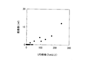
同様にして、裏面LPDの個数と割れ発生率との関係を測定した。
ウェーハ裏面に存在するCrackや傷を測定する手段としては、レーザ光散乱式パーティクルカウンター(SP1もしくはSP2等:KLA-Tencor社製)を用いてLPDとして検出することが可能である。本実験例は、裏面LPD数の異なる300mmウェーハに対してFLA炉を用いて割れ試験を実施した例である。割れ発生率は各水準100枚のウェーハを処理した際に割れ発生した率である。
その結果を表5に示す。

Wr 裏面
Wo 中心
Claims (6)
- シリコンウェーハの製造方法であって、
シリコン単結晶のインゴットをスライスし、そのスライスされたシリコンウェーハの表面処理を行うウェーハ準備工程と、
前記ウェーハ準備工程において準備した前記シリコンウェーハにかかる応力S(MPa)を設定する応力設定工程と、
前記シリコンウェーハの表面または裏面に存在する傷を検査する検査工程と、
前記検査工程において検査したシリコンウェーハが、下記式(A)の基準を満たすか否かを判定し、基準を満たすシリコンウェーハを合格、基準を満たさないシリコンウェーハを不合格とする判定工程と
応力S×傷の大きさC≦3500(MPa・μm)…(A)
C:シリコンウェーハ表面または裏面に存在する傷の大きさ(μm)
を備えるシリコンウェーハの製造方法。 - 前記応力Sが熱処理に依存するとき、
前記熱処理における処理条件は、処理温度を1100℃以上シリコンの融点以下とし、処理時間を1μ秒から100m秒程度までとする請求項1記載のシリコンウェーハの製造方法。 - 前記検査工程においてあるシリコンウェーハの裏面における大きさ2μm以上のLPDが10個以下であることが判明したとき、前記判定工程においてそのシリコンウェーハが上記(A)の基準を満たすと判定する請求項1または2記載のシリコンウェーハの製造方法。
- 前記判定工程において上記(A)の基準を満たさないと判定されたシリコンウェーハを、前記ウェーハ準備工程において再度表面処理する請求項1から3のいずれか記載のシリコンウェーハの製造方法。
- 前記シリコンウェーハの酸素濃度Oiを、5×10¹⁷~20×1017atoms/cm3 (Old-ASTM)に設定する請求項1から4のいずれか記載のシリコンウェーハの製造方法。
- 請求項1から5のいずれか記載のシリコンウェーハの製造方法により製造されるシリコンウェーハ。
Priority Applications (3)
| Application Number | Priority Date | Filing Date | Title |
|---|---|---|---|
| KR1020117022890A KR101272711B1 (ko) | 2009-03-25 | 2010-03-24 | 실리콘 웨이퍼 및 그 제조방법 |
| CN201080013892.9A CN102362017B (zh) | 2009-03-25 | 2010-03-24 | 硅晶片及其制造方法 |
| US13/258,702 US8765492B2 (en) | 2009-03-25 | 2010-03-24 | Silicon wafer and method of manufacturing same |
Applications Claiming Priority (2)
| Application Number | Priority Date | Filing Date | Title |
|---|---|---|---|
| JP2009-074947 | 2009-03-25 | ||
| JP2009074947A JP5407473B2 (ja) | 2009-03-25 | 2009-03-25 | シリコンウェーハの製造方法 |
Publications (1)
| Publication Number | Publication Date |
|---|---|
| WO2010109853A1 true WO2010109853A1 (ja) | 2010-09-30 |
Family
ID=42780550
Family Applications (1)
| Application Number | Title | Priority Date | Filing Date |
|---|---|---|---|
| PCT/JP2010/002060 Ceased WO2010109853A1 (ja) | 2009-03-25 | 2010-03-24 | シリコンウェーハおよびその製造方法 |
Country Status (6)
| Country | Link |
|---|---|
| US (1) | US8765492B2 (ja) |
| JP (1) | JP5407473B2 (ja) |
| KR (1) | KR101272711B1 (ja) |
| CN (1) | CN102362017B (ja) |
| TW (1) | TWI412639B (ja) |
| WO (1) | WO2010109853A1 (ja) |
Cited By (1)
| Publication number | Priority date | Publication date | Assignee | Title |
|---|---|---|---|---|
| JP2024041146A (ja) * | 2022-09-14 | 2024-03-27 | 株式会社Screenホールディングス | 熱処理方法および熱処理装置 |
Families Citing this family (14)
| Publication number | Priority date | Publication date | Assignee | Title |
|---|---|---|---|---|
| JP5606852B2 (ja) * | 2010-09-27 | 2014-10-15 | 大日本スクリーン製造株式会社 | 熱処理装置および熱処理方法 |
| KR101208960B1 (ko) * | 2010-11-26 | 2012-12-06 | 에스케이하이닉스 주식회사 | 반도체 장치 및 이의 테스트 방법 |
| TWI510682B (zh) * | 2011-01-28 | 2015-12-01 | Sino American Silicon Prod Inc | 晶棒表面奈米化製程、晶圓製造方法及其晶圓 |
| JP6056749B2 (ja) * | 2013-12-25 | 2017-01-11 | 信越半導体株式会社 | エピタキシャル成長前後の半導体ウェーハのエッジ形状の評価方法 |
| JP6083404B2 (ja) * | 2014-03-17 | 2017-02-22 | 信越半導体株式会社 | 半導体基板の評価方法 |
| CN103972126A (zh) * | 2014-05-21 | 2014-08-06 | 上海华力微电子有限公司 | 预防硅片破片的方法 |
| KR101895817B1 (ko) * | 2014-06-02 | 2018-09-07 | 가부시키가이샤 사무코 | 실리콘 웨이퍼 및 그 제조 방법 |
| WO2017116687A1 (en) * | 2015-12-30 | 2017-07-06 | Mattson Technology, Inc. | Substrate breakage detection in a thermal processing system |
| CN106256477A (zh) * | 2016-08-31 | 2016-12-28 | 安徽芯瑞达电子科技有限公司 | 暗部判断法激光切割方法 |
| DE102018203945B4 (de) * | 2018-03-15 | 2023-08-10 | Siltronic Ag | Verfahren zur Herstellung von Halbleiterscheiben |
| JP7351273B2 (ja) * | 2020-08-25 | 2023-09-27 | 株式会社Sumco | 半導体ウェーハの割れの発生率低減方法 |
| JP7847419B2 (ja) * | 2021-08-06 | 2026-04-17 | グローバルウェーハズ・ジャパン株式会社 | シリコンウェーハ用サセプタの前処理方法およびシリコンウェーハの熱処理方法 |
| CN118647736A (zh) * | 2022-01-10 | 2024-09-13 | 海德鲁挤压美国有限责任公司 | 用于自动喷雾淬火的系统和方法 |
| JP7813607B2 (ja) * | 2022-02-28 | 2026-02-13 | 株式会社Screenホールディングス | 熱処理装置および熱処理方法 |
Citations (4)
| Publication number | Priority date | Publication date | Assignee | Title |
|---|---|---|---|---|
| JP2004319642A (ja) * | 2003-04-14 | 2004-11-11 | Sumitomo Mitsubishi Silicon Corp | Soi基板の製造方法およびsoi基板 |
| WO2006003812A1 (ja) * | 2004-06-30 | 2006-01-12 | Sumitomo Mitsubishi Silicon Corporation | シリコンウェーハの製造方法及びこの方法により製造されたシリコンウェーハ |
| JP2008306206A (ja) * | 2008-08-04 | 2008-12-18 | Sumco Corp | シリコンエピタキシャルウェーハとその製造方法 |
| JP2009023851A (ja) * | 2007-07-17 | 2009-02-05 | Sumco Corp | シリコン単結晶製造用原料の製造方法およびシリコン単結晶の製造方法 |
Family Cites Families (13)
| Publication number | Priority date | Publication date | Assignee | Title |
|---|---|---|---|---|
| WO1996022844A1 (en) * | 1995-01-27 | 1996-08-01 | Trustees Of Boston University | Acoustic coaxing methods and apparatus |
| JP4525871B2 (ja) * | 1999-05-07 | 2010-08-18 | 株式会社ニューフレアテクノロジー | ウエハ熱処理装置及びそれを用いたウエハの熱処理方法 |
| WO2004008521A1 (ja) | 2002-07-17 | 2004-01-22 | Sumitomo Mitsubishi Silicon Corporation | 高抵抗シリコンウエーハ及びその製造方法 |
| KR100573473B1 (ko) | 2004-05-10 | 2006-04-24 | 주식회사 실트론 | 실리콘 웨이퍼 및 그 제조방법 |
| KR100798585B1 (ko) * | 2004-06-30 | 2008-01-28 | 가부시키가이샤 섬코 | 실리콘 웨이퍼의 제조 방법 및 이 방법에 의해 제조된실리콘 웨이퍼 |
| JP2006045007A (ja) | 2004-08-05 | 2006-02-16 | Komatsu Electronic Metals Co Ltd | シリコン単結晶の品質評価方法 |
| US7102141B2 (en) | 2004-09-28 | 2006-09-05 | Intel Corporation | Flash lamp annealing apparatus to generate electromagnetic radiation having selective wavelengths |
| DE102005013831B4 (de) * | 2005-03-24 | 2008-10-16 | Siltronic Ag | Siliciumscheibe und Verfahren zur thermischen Behandlung einer Siliciumscheibe |
| JP5239155B2 (ja) * | 2006-06-20 | 2013-07-17 | 信越半導体株式会社 | シリコンウエーハの製造方法 |
| JP5119677B2 (ja) * | 2007-02-16 | 2013-01-16 | 株式会社Sumco | シリコンウェーハ及びその製造方法 |
| JP2008098640A (ja) | 2007-10-09 | 2008-04-24 | Toshiba Corp | 半導体装置の製造方法 |
| JP2009259959A (ja) * | 2008-04-15 | 2009-11-05 | Sumco Corp | 薄厚シリコンウェーハおよびその製造方法 |
| US8143078B2 (en) * | 2009-12-23 | 2012-03-27 | Memc Electronic Materials, Inc. | Methods for monitoring the amount of contamination imparted into semiconductor wafers during wafer processing |
-
2009
- 2009-03-25 JP JP2009074947A patent/JP5407473B2/ja active Active
-
2010
- 2010-03-24 CN CN201080013892.9A patent/CN102362017B/zh active Active
- 2010-03-24 WO PCT/JP2010/002060 patent/WO2010109853A1/ja not_active Ceased
- 2010-03-24 KR KR1020117022890A patent/KR101272711B1/ko active Active
- 2010-03-24 US US13/258,702 patent/US8765492B2/en active Active
- 2010-03-25 TW TW099108918A patent/TWI412639B/zh active
Patent Citations (4)
| Publication number | Priority date | Publication date | Assignee | Title |
|---|---|---|---|---|
| JP2004319642A (ja) * | 2003-04-14 | 2004-11-11 | Sumitomo Mitsubishi Silicon Corp | Soi基板の製造方法およびsoi基板 |
| WO2006003812A1 (ja) * | 2004-06-30 | 2006-01-12 | Sumitomo Mitsubishi Silicon Corporation | シリコンウェーハの製造方法及びこの方法により製造されたシリコンウェーハ |
| JP2009023851A (ja) * | 2007-07-17 | 2009-02-05 | Sumco Corp | シリコン単結晶製造用原料の製造方法およびシリコン単結晶の製造方法 |
| JP2008306206A (ja) * | 2008-08-04 | 2008-12-18 | Sumco Corp | シリコンエピタキシャルウェーハとその製造方法 |
Cited By (1)
| Publication number | Priority date | Publication date | Assignee | Title |
|---|---|---|---|---|
| JP2024041146A (ja) * | 2022-09-14 | 2024-03-27 | 株式会社Screenホールディングス | 熱処理方法および熱処理装置 |
Also Published As
| Publication number | Publication date |
|---|---|
| TW201040332A (en) | 2010-11-16 |
| US20120012983A1 (en) | 2012-01-19 |
| CN102362017B (zh) | 2014-06-11 |
| KR101272711B1 (ko) | 2013-06-10 |
| KR20110132419A (ko) | 2011-12-07 |
| US8765492B2 (en) | 2014-07-01 |
| JP5407473B2 (ja) | 2014-02-05 |
| TWI412639B (zh) | 2013-10-21 |
| JP2010228929A (ja) | 2010-10-14 |
| CN102362017A (zh) | 2012-02-22 |
Similar Documents
| Publication | Publication Date | Title |
|---|---|---|
| JP5407473B2 (ja) | シリコンウェーハの製造方法 | |
| CN101139733B (zh) | 具有缺陷减少区域的单晶半导体晶片及其制造方法 | |
| US7838431B2 (en) | Method for surface treatment of semiconductor substrates | |
| WO2013179804A1 (ja) | 半導体装置の製造方法およびアニール方法 | |
| JP5504664B2 (ja) | シリコンエピタキシャルウェーハおよびその製造方法 | |
| JP5569392B2 (ja) | シリコンウェーハの製造方法 | |
| JP2004179510A (ja) | 熱処理装置および熱処理用サセプタ | |
| JP4272445B2 (ja) | 熱処理装置 | |
| JP2010073787A (ja) | 熱処理装置 | |
| CN103069545B (zh) | 晶片的热处理方法、硅晶片的制造方法、硅晶片及热处理装置 | |
| JP5504667B2 (ja) | シリコンウェーハおよびその製造方法 | |
| JP5613994B2 (ja) | シリコンウェーハおよびその製造方法 | |
| US8193071B2 (en) | Method for manufacturing semiconductor device | |
| TW200818321A (en) | Semiconductor on insulator structure made using radiation annealing | |
| US20080268660A1 (en) | Method of manufacturing semiconductor device | |
| JP5811218B2 (ja) | シリコンエピタキシャルウェーハの製造方法 | |
| TWI867950B (zh) | 半導體晶圓的製造方法以及半導體器件的製造方法 | |
| US7906443B2 (en) | Controlling oxygen precipitates in silicon wafers using infrared irradiation and heating | |
| JP2014111545A (ja) | シリコンウェーハの製造方法 |
Legal Events
| Date | Code | Title | Description |
|---|---|---|---|
| WWE | Wipo information: entry into national phase |
Ref document number: 201080013892.9 Country of ref document: CN |
|
| 121 | Ep: the epo has been informed by wipo that ep was designated in this application |
Ref document number: 10755655 Country of ref document: EP Kind code of ref document: A1 |
|
| WWE | Wipo information: entry into national phase |
Ref document number: 13258702 Country of ref document: US |
|
| NENP | Non-entry into the national phase |
Ref country code: DE |
|
| ENP | Entry into the national phase |
Ref document number: 20117022890 Country of ref document: KR Kind code of ref document: A |
|
| 122 | Ep: pct application non-entry in european phase |
Ref document number: 10755655 Country of ref document: EP Kind code of ref document: A1 |