WO2010106859A1 - 化学気相成長用原料及びこれを用いたシリコン含有薄膜形成方法 - Google Patents
化学気相成長用原料及びこれを用いたシリコン含有薄膜形成方法 Download PDFInfo
- Publication number
- WO2010106859A1 WO2010106859A1 PCT/JP2010/052200 JP2010052200W WO2010106859A1 WO 2010106859 A1 WO2010106859 A1 WO 2010106859A1 JP 2010052200 W JP2010052200 W JP 2010052200W WO 2010106859 A1 WO2010106859 A1 WO 2010106859A1
- Authority
- WO
- WIPO (PCT)
- Prior art keywords
- thin film
- vapor deposition
- chemical vapor
- silicon
- raw material
- Prior art date
- Legal status (The legal status is an assumption and is not a legal conclusion. Google has not performed a legal analysis and makes no representation as to the accuracy of the status listed.)
- Ceased
Links
Images

Classifications
-
- C—CHEMISTRY; METALLURGY
- C23—COATING METALLIC MATERIAL; COATING MATERIAL WITH METALLIC MATERIAL; CHEMICAL SURFACE TREATMENT; DIFFUSION TREATMENT OF METALLIC MATERIAL; COATING BY VACUUM EVAPORATION, BY SPUTTERING, BY ION IMPLANTATION OR BY CHEMICAL VAPOUR DEPOSITION, IN GENERAL; INHIBITING CORROSION OF METALLIC MATERIAL OR INCRUSTATION IN GENERAL
- C23C—COATING METALLIC MATERIAL; COATING MATERIAL WITH METALLIC MATERIAL; SURFACE TREATMENT OF METALLIC MATERIAL BY DIFFUSION INTO THE SURFACE, BY CHEMICAL CONVERSION OR SUBSTITUTION; COATING BY VACUUM EVAPORATION, BY SPUTTERING, BY ION IMPLANTATION OR BY CHEMICAL VAPOUR DEPOSITION, IN GENERAL
- C23C16/00—Chemical coating by decomposition of gaseous compounds, without leaving reaction products of surface material in the coating, i.e. chemical vapour deposition [CVD] processes
- C23C16/22—Chemical coating by decomposition of gaseous compounds, without leaving reaction products of surface material in the coating, i.e. chemical vapour deposition [CVD] processes characterised by the deposition of inorganic material, other than metallic material
- C23C16/30—Deposition of compounds, mixtures or solid solutions, e.g. borides, carbides, nitrides
- C23C16/34—Nitrides
- C23C16/345—Silicon nitride
-
- C—CHEMISTRY; METALLURGY
- C07—ORGANIC CHEMISTRY
- C07F—ACYCLIC, CARBOCYCLIC OR HETEROCYCLIC COMPOUNDS CONTAINING ELEMENTS OTHER THAN CARBON, HYDROGEN, HALOGEN, OXYGEN, NITROGEN, SULFUR, SELENIUM OR TELLURIUM
- C07F7/00—Compounds containing elements of Groups 4 or 14 of the Periodic Table
- C07F7/02—Silicon compounds
- C07F7/025—Silicon compounds without C-silicon linkages
-
- C—CHEMISTRY; METALLURGY
- C23—COATING METALLIC MATERIAL; COATING MATERIAL WITH METALLIC MATERIAL; CHEMICAL SURFACE TREATMENT; DIFFUSION TREATMENT OF METALLIC MATERIAL; COATING BY VACUUM EVAPORATION, BY SPUTTERING, BY ION IMPLANTATION OR BY CHEMICAL VAPOUR DEPOSITION, IN GENERAL; INHIBITING CORROSION OF METALLIC MATERIAL OR INCRUSTATION IN GENERAL
- C23C—COATING METALLIC MATERIAL; COATING MATERIAL WITH METALLIC MATERIAL; SURFACE TREATMENT OF METALLIC MATERIAL BY DIFFUSION INTO THE SURFACE, BY CHEMICAL CONVERSION OR SUBSTITUTION; COATING BY VACUUM EVAPORATION, BY SPUTTERING, BY ION IMPLANTATION OR BY CHEMICAL VAPOUR DEPOSITION, IN GENERAL
- C23C16/00—Chemical coating by decomposition of gaseous compounds, without leaving reaction products of surface material in the coating, i.e. chemical vapour deposition [CVD] processes
- C23C16/22—Chemical coating by decomposition of gaseous compounds, without leaving reaction products of surface material in the coating, i.e. chemical vapour deposition [CVD] processes characterised by the deposition of inorganic material, other than metallic material
- C23C16/30—Deposition of compounds, mixtures or solid solutions, e.g. borides, carbides, nitrides
- C23C16/32—Carbides
- C23C16/325—Silicon carbide
-
- C—CHEMISTRY; METALLURGY
- C23—COATING METALLIC MATERIAL; COATING MATERIAL WITH METALLIC MATERIAL; CHEMICAL SURFACE TREATMENT; DIFFUSION TREATMENT OF METALLIC MATERIAL; COATING BY VACUUM EVAPORATION, BY SPUTTERING, BY ION IMPLANTATION OR BY CHEMICAL VAPOUR DEPOSITION, IN GENERAL; INHIBITING CORROSION OF METALLIC MATERIAL OR INCRUSTATION IN GENERAL
- C23C—COATING METALLIC MATERIAL; COATING MATERIAL WITH METALLIC MATERIAL; SURFACE TREATMENT OF METALLIC MATERIAL BY DIFFUSION INTO THE SURFACE, BY CHEMICAL CONVERSION OR SUBSTITUTION; COATING BY VACUUM EVAPORATION, BY SPUTTERING, BY ION IMPLANTATION OR BY CHEMICAL VAPOUR DEPOSITION, IN GENERAL
- C23C16/00—Chemical coating by decomposition of gaseous compounds, without leaving reaction products of surface material in the coating, i.e. chemical vapour deposition [CVD] processes
- C23C16/22—Chemical coating by decomposition of gaseous compounds, without leaving reaction products of surface material in the coating, i.e. chemical vapour deposition [CVD] processes characterised by the deposition of inorganic material, other than metallic material
- C23C16/30—Deposition of compounds, mixtures or solid solutions, e.g. borides, carbides, nitrides
- C23C16/40—Oxides
- C23C16/401—Oxides containing silicon
- C23C16/402—Silicon dioxide
-
- C—CHEMISTRY; METALLURGY
- C23—COATING METALLIC MATERIAL; COATING MATERIAL WITH METALLIC MATERIAL; CHEMICAL SURFACE TREATMENT; DIFFUSION TREATMENT OF METALLIC MATERIAL; COATING BY VACUUM EVAPORATION, BY SPUTTERING, BY ION IMPLANTATION OR BY CHEMICAL VAPOUR DEPOSITION, IN GENERAL; INHIBITING CORROSION OF METALLIC MATERIAL OR INCRUSTATION IN GENERAL
- C23C—COATING METALLIC MATERIAL; COATING MATERIAL WITH METALLIC MATERIAL; SURFACE TREATMENT OF METALLIC MATERIAL BY DIFFUSION INTO THE SURFACE, BY CHEMICAL CONVERSION OR SUBSTITUTION; COATING BY VACUUM EVAPORATION, BY SPUTTERING, BY ION IMPLANTATION OR BY CHEMICAL VAPOUR DEPOSITION, IN GENERAL
- C23C16/00—Chemical coating by decomposition of gaseous compounds, without leaving reaction products of surface material in the coating, i.e. chemical vapour deposition [CVD] processes
- C23C16/44—Chemical coating by decomposition of gaseous compounds, without leaving reaction products of surface material in the coating, i.e. chemical vapour deposition [CVD] processes characterised by the method of coating
- C23C16/455—Chemical coating by decomposition of gaseous compounds, without leaving reaction products of surface material in the coating, i.e. chemical vapour deposition [CVD] processes characterised by the method of coating characterised by the method used for introducing gases into reaction chamber or for modifying gas flows in reaction chamber
- C23C16/45523—Pulsed gas flow or change of composition over time
- C23C16/45525—Atomic layer deposition [ALD]
- C23C16/45553—Atomic layer deposition [ALD] characterized by the use of precursors specially adapted for ALD
-
- H—ELECTRICITY
- H10—SEMICONDUCTOR DEVICES; ELECTRIC SOLID-STATE DEVICES NOT OTHERWISE PROVIDED FOR
- H10P—GENERIC PROCESSES OR APPARATUS FOR THE MANUFACTURE OR TREATMENT OF DEVICES COVERED BY CLASS H10
- H10P14/00—Formation of materials, e.g. in the shape of layers or pillars
- H10P14/20—Formation of materials, e.g. in the shape of layers or pillars of semiconductor materials
- H10P14/24—Formation of materials, e.g. in the shape of layers or pillars of semiconductor materials using chemical vapour deposition [CVD]
-
- H—ELECTRICITY
- H10—SEMICONDUCTOR DEVICES; ELECTRIC SOLID-STATE DEVICES NOT OTHERWISE PROVIDED FOR
- H10P—GENERIC PROCESSES OR APPARATUS FOR THE MANUFACTURE OR TREATMENT OF DEVICES COVERED BY CLASS H10
- H10P14/00—Formation of materials, e.g. in the shape of layers or pillars
- H10P14/60—Formation of materials, e.g. in the shape of layers or pillars of insulating materials
- H10P14/63—Formation of materials, e.g. in the shape of layers or pillars of insulating materials characterised by the formation processes
- H10P14/6326—Deposition processes
- H10P14/6328—Deposition from the gas or vapour phase
- H10P14/6334—Deposition from the gas or vapour phase using decomposition or reaction of gaseous or vapour phase compounds, i.e. chemical vapour deposition
- H10P14/6339—Deposition from the gas or vapour phase using decomposition or reaction of gaseous or vapour phase compounds, i.e. chemical vapour deposition deposition by cyclic CVD, e.g. ALD, ALE or pulsed CVD
-
- H—ELECTRICITY
- H10—SEMICONDUCTOR DEVICES; ELECTRIC SOLID-STATE DEVICES NOT OTHERWISE PROVIDED FOR
- H10P—GENERIC PROCESSES OR APPARATUS FOR THE MANUFACTURE OR TREATMENT OF DEVICES COVERED BY CLASS H10
- H10P14/00—Formation of materials, e.g. in the shape of layers or pillars
- H10P14/60—Formation of materials, e.g. in the shape of layers or pillars of insulating materials
- H10P14/66—Formation of materials, e.g. in the shape of layers or pillars of insulating materials characterised by the type of materials
- H10P14/668—Formation of materials, e.g. in the shape of layers or pillars of insulating materials characterised by the type of materials the materials being characterised by the deposition precursor materials
- H10P14/6681—Formation of materials, e.g. in the shape of layers or pillars of insulating materials characterised by the type of materials the materials being characterised by the deposition precursor materials the precursor containing a compound comprising Si
- H10P14/6687—Formation of materials, e.g. in the shape of layers or pillars of insulating materials characterised by the type of materials the materials being characterised by the deposition precursor materials the precursor containing a compound comprising Si the compound comprising silicon and nitrogen
- H10P14/6689—Formation of materials, e.g. in the shape of layers or pillars of insulating materials characterised by the type of materials the materials being characterised by the deposition precursor materials the precursor containing a compound comprising Si the compound comprising silicon and nitrogen the compound being a silazane
-
- H—ELECTRICITY
- H10—SEMICONDUCTOR DEVICES; ELECTRIC SOLID-STATE DEVICES NOT OTHERWISE PROVIDED FOR
- H10P—GENERIC PROCESSES OR APPARATUS FOR THE MANUFACTURE OR TREATMENT OF DEVICES COVERED BY CLASS H10
- H10P14/00—Formation of materials, e.g. in the shape of layers or pillars
- H10P14/60—Formation of materials, e.g. in the shape of layers or pillars of insulating materials
- H10P14/69—Inorganic materials
- H10P14/694—Inorganic materials composed of nitrides
- H10P14/6943—Inorganic materials composed of nitrides containing silicon
- H10P14/69433—Inorganic materials composed of nitrides containing silicon the material being a silicon nitride not containing oxygen, e.g. SixNy or SixByNz
Definitions
- the present invention relates to a raw material for chemical vapor deposition containing an organic silicon-containing compound having a specific structure, and a method for forming a silicon-containing thin film by chemical vapor deposition using the raw material.
- Silicon-containing thin films are used as electronic members for electronic components such as capacitor films, gate films, barrier films, and gate insulating films, and as optical members for optical communication devices such as optical waveguides, optical switches, and optical amplifiers.
- electronic members As electronic devices are highly integrated and densified, the electronic members and optical members tend to be miniaturized. In such a situation, the silicon-containing thin film is desired to be thinner.
- a silicon nitride thin film is used instead of the conventional silicon oxide thin film.
- Examples of the method for forming the silicon-containing thin film include a coating pyrolysis method, a sol-gel method, a chemical vapor deposition method (hereinafter referred to as a CVD method), and an atomic layer deposition method (hereinafter referred to as an ALD method). Since it has many advantages such as excellent properties and step coverage, suitable for mass production, and capable of hybrid integration, the most suitable method is to vaporize a precursor such as CVD or ALD. This is a thin film forming method.
- inorganic chlorosilanes such as dichlorosilane and hexachlorodisilane are generally used as precursors for the above CVD method and ALD method.
- this method it is necessary to form a film at a high temperature of 700 to 900.degree. Therefore, there is a problem that it cannot be used for a process in which the wafer temperature cannot be raised, such as after metal wiring.
- Another problem is that impurities in the shallow diffusion layer are diffused deeply by heat, making it difficult to reduce the size of the electronic member.
- Patent Document 1 discloses a technique for forming a Si 3 N 4 film by a CVD method using SiH 2 (NH (C 4 H 9 )) 2 (Bis tertiary butylamino silane: BTBAS) as a precursor. Yes.
- Patent Document 2 discloses SiCl (N (C 2 H 5 ) 2 ) 3 , SiCl (NH (C 2 H 5 )) 3 , SiH 2 (N (C 3 H 7 ) 2 ) 2 , or Si A film forming technique using (N (CH 3 ) 2 ) 4 as a precursor is disclosed.
- Patent Document 1 and Patent Document 2 are film formation techniques at a film formation temperature of 600 to 800 ° C., and it cannot be said that the film formation temperature can be sufficiently lowered.
- the problem to be solved by the present invention is a chemical vapor deposition material comprising an organic silicon-containing compound that can form a film at a low temperature of 300 to 500 ° C. and further provides a process with good reactivity. Is to provide.
- HSiCl (NR 1 R 2 ) (NR 3 R 4 ) (R 1 and R 3 represent an alkyl group having 1 to 4 carbon atoms or hydrogen, and R 2 and R 4 represent 1 to 4 carbon atoms.
- the present invention also provides a method for forming a silicon-containing thin film by chemical vapor deposition using the above chemical vapor deposition raw material.
- a raw material for chemical vapor deposition containing an organic silicon-containing compound capable of forming a film at a low temperature of 300 to 500 ° C. and further providing a process with good reactivity.
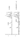
- FIG. 1 shows the compound No. measured in Evaluation Example 2.
- 8 is an FT-IR spectrum before and after NH 3 gas blowing at room temperature.
- 2 shows the compound No. measured in Evaluation Example 2.
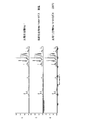
- 8 is an FT-IR spectrum before and after NH 3 gas blowing at 200 ° C. in FIG. 3 shows comparative compound No. 1 measured in Evaluation Example 2.
- 1 is an FT-IR spectrum before and after NH 3 gas blowing at room temperature and 200 ° C.
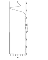
- FIG. FIG. 4 shows the results of evaluation of Compound No. 3 after NH 3 gas blowing at room temperature in Evaluation Example 3.
- 8 is an FT-IR spectrum when 8 is baked at 700 ° C. on a Si wafer.
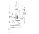
- FIG. 5 is a schematic view showing an example of an ALD apparatus used in the thin film forming method of the present invention.
- the chemical vapor deposition material of the present invention has a general formula HSiCl (NR 1 R 2 ) (NR 3 R 4 ) (R 1 and R 3 represent an alkyl group having 1 to 4 carbon atoms or hydrogen, R 2 , R 3 4 represents an alkyl group having 1 to 4 carbon atoms) as a precursor of a thin film, and includes silicon oxide containing silicon oxide, silicon nitride, silicon carbonitride, silicon and others. It can be used to form a thin film such as a complex oxide with a metal element. In particular, it is suitable as a raw material for chemical vapor deposition for low-temperature deposition of a silicon nitride thin film. In the present invention, the chemical vapor deposition raw material represents both a CVD raw material and an ALD raw material unless otherwise distinguished.
- the above-mentioned organic silicon-containing compound is characterized by having hydrogen, chlorine and amino groups that are bonded to silicon.
- the chlorine contained in the organic silicon-containing compound improves the reactivity and improves the film formation rate. Furthermore, since the organic silicon-containing compound also has an amino group, film formation at a low temperature is possible.
- Examples of the alkyl group having 1 to 4 carbon atoms represented by R 1 and R 2 in the above general formula include methyl, ethyl, propyl, 2-propyl, butyl, 2-butyl, isobutyl, tertiary butyl and the like.
- R 1 and R 3 contained in the above general formula may be the same or different. The same applies to R 2 and R 4 .
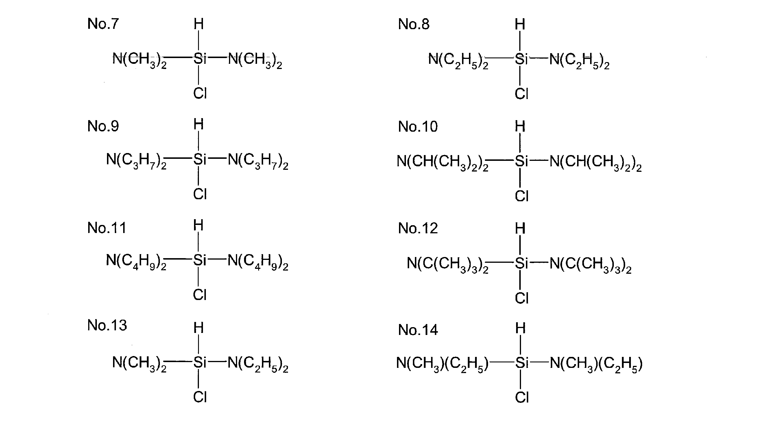
- organic silicon-containing compound represented by the above general formula examples include the following compound Nos. 1-No. 14 is mentioned.
- R 1 to R 4 are alkyl groups having a small number of carbon atoms (particularly those having 2 or less carbon atoms).
- the organosilicon-containing compound represented by the general formula HSiCl (NR 1 R 2 ) (NR 3 R 4 ) can be synthesized by applying a conventionally known reaction.
- trichlorosilane may be reacted with a primary amine or secondary amine corresponding to the amino group (—NR 1 R 2 and —NR 3 R 4 ) of the target organic silicon-containing compound.
- This reaction is carried out by ether solvents such as methyl tertiary butyl ether, diethyl ether, 1,2-dimethoxyethane, 1,2-diethoxyethane, diglyme; THF; tetrahydropyran; normal pentane, normal hexane, normal heptane, etc.
- the reaction ratio is preferably in the range of 1.8 to 3.0 mol of primary amine or secondary amine with respect to 1 mol of trichlorosilane.
- the reaction temperature is preferably ⁇ 70 to 60 ° C., and the reaction time is preferably 12 hours or less.
- the raw material for chemical vapor deposition of the present invention contains the above-mentioned organic silicon-containing compound, and is an organic silicon-containing compound itself or a composition containing the same.
- the raw material for chemical vapor deposition according to the present invention is appropriately selected according to a method such as a transport supply method of chemical vapor deposition used.
- the chemical vapor deposition raw material is vaporized by heating and / or depressurizing in the raw material container and used as necessary.
- Gas transport method that introduces into the deposition reaction part together with a carrier gas such as argon, nitrogen, helium, etc., transports the raw material for chemical vapor deposition to the vaporization chamber in a liquid or solution state, and heats and / or decompresses in the vaporization chamber
- a liquid transport method in which the gas is vaporized and introduced into the deposition reaction part.
- the organic silicon-containing compound itself represented by the general formula HSiCl (NR 1 R 2 ) (NR 3 R 4 ) itself is a raw material for chemical vapor deposition.
- the organic silicon-containing compound itself represented by the formula HSiCl (NR 1 R 2 ) (NR 3 R 4 ) or a solution obtained by dissolving the compound in an organic solvent is a raw material for chemical vapor deposition.
- a chemical vapor deposition material is vaporized and supplied independently for each component (hereinafter referred to as a single source method), There is a method of vaporizing and supplying a mixed raw material in which component raw materials are previously mixed in a desired composition (hereinafter referred to as a cocktail sauce method).
- a mixture of only the organic silicon-containing compound represented by the general formula HSiCl (NR 1 R 2 ) (NR 3 R 4 ) or a mixed solution obtained by adding an organic solvent to the mixture the general formula HSiCl ( A mixture of an organic silicon-containing compound represented by NR 1 R 2 ) (NR 3 R 4 ) and another precursor or a mixed solution obtained by adding an organic solvent to these mixtures is a raw material for chemical vapor deposition.
- the organic solvent used for the chemical vapor deposition raw material is not particularly limited and is a well-known general organic solvent that does not react with the organic silicon-containing compound and other precursors used as necessary. Can be used.
- the organic solvent include: acetates such as ethyl acetate, butyl acetate and methoxyethyl acetate; ethers such as tetrahydrofuran, tetrahydropyran, morpholine, ethylene glycol dimethyl ether, diethylene glycol dimethyl ether, triethylene glycol dimethyl ether, dibutyl ether and dioxane Ketones such as methyl butyl ketone, methyl isobutyl ketone, ethyl butyl ketone, dipropyl ketone, diisobutyl ketone, methyl amyl ketone, cyclohexanone, methylcyclohexanone; hexane, cyclohexane, methyl
- hydrocarbons having a cyano group include pyridine and lutidine, and these are used alone or as a mixed solvent of two or more kinds depending on the solubility of the solute, the relationship between the use temperature and boiling point, the flash point, and the like.
- the total amount of the precursor components in the organic solvent is 0.01 to 2.0 mol / liter, particularly 0.05 to 1.0 mol / liter. .
- precursors are selected from the group consisting of compounds used as organic ligands such as alcohol compounds, glycol compounds, ⁇ -diketone compounds, cyclopentadiene compounds, and organic amine compounds. Or a compound of one or more of these and a metal element.
- the above-mentioned precursor metal species other than silicon include group 1 elements such as lithium, sodium, potassium, rubidium and cesium, group 2 elements such as beryllium, magnesium, calcium, strontium and barium, scandium, yttrium and lanthanoid elements.
- group 3 elements such as actinoid elements, group 4 elements of titanium, zirconium, hafnium, Vanadium, niobium, tantalum group 5 elements, chromium, molybdenum, tungsten group 6 elements, manganese, technetium, rhenium group 7 elements, iron, ruthenium, male Group 8 element of Um, Group 9 element of Cobalt, Rhodium, Iridium, Group 10 element of Nickel, Palladium, Platinum, Group 11 element of Copper, Silver, Gold, Group 12 element of Zinc, Cadmium, Mercury, Aluminum, Gallium, Examples include group 13 elements of indium and thallium, group 14 elements of germanium, tin and lead,
- Examples of the alcohol compound used as the organic ligand include methanol, ethanol, propanol, isopropanol, butanol, 2-butanol, isobutanol, tertiary butanol, amyl alcohol, isoamino alcohol, and tertiary amino alcohol.
- Alkyl alcohols 2-methoxyethanol, 2-ethoxyethanol, 2-butoxyethanol, 2- (2-methoxyethoxy) ethanol, 2-methoxy-1-methylethanol, 2-methoxy-1,1-dimethylethanol, 2 Isopropoxy-1,1-dimethylethanol, 2-butoxy-1,1-dimethylethanol, 2- (2-methoxyethoxy) -1,1-dimethylethanol, 2-propoxy-1,1-diethylethanol, 2 -2nd butto Ether alcohols such as cis-1,1-diethylethanol, 3-methoxy-1,1-dimethylpropanol, N, N-dimethylaminoethanol, 1,1-dimethylamino-2-propanol, 1,1-dimethylamino And dialkylamino alcohols such as -2-methyl-2-propanol.
- glycol compound used as the organic ligand examples include 1,2-ethanediol, 1,2-propanediol, 1,3-propanediol, 2,4-hexanediol, 1,2-propanediol, , 3-propanediol, 2,4-hexanediol, 2,2-dimethyl-1,3-propanediol, 2,2-diethyl-1,3-propanediol, 1,3-butanediol, 2,4- Butanediol, 2,2-diethyl-1,3-butanediol, 2-ethyl-2-butyl-1,3-propanediol, 2,4-pentanediol, 2-methyl-1,3-propanediol, 2 -Methyl-2,4-pentanediol, 2,4-hexanediol, 2,4-dimethyl-2,4-
- Examples of the ⁇ -diketone compound used as the organic ligand include acetylacetone, hexane-2,4-dione, 5-methylhexane-2,4-dione, heptane-2,4-dione, 2- Methylheptane-3,5-dione, 5-methylheptane-2,4-dione, 6-methylheptane-2,4-dione, 2,2-dimethylheptane-3,5-dione, 2,6-dimethylheptane -3,5-dione, 2,2,6-trimethylheptane-3,5-dione, 2,2,6,6-tetramethylheptane-3,5-dione, octane-2,4-dione, 2, 2,6-trimethyloctane-3,5-dione, 2,6-dimethyloctane-3,5-dione, 2,2-dimethyl-6-ethyloctane-3,5
- cyclopentadiene compound used as the organic ligand examples include cyclopentadiene, methylcyclopentadiene, ethylcyclopentadiene, propylcyclopentadiene, isopropylcyclopentadiene, butylcyclopentadiene, second butylcyclopentadiene, isobutylcyclopentadiene, third Examples include butylcyclopentadiene, dimethylcyclopentadiene, and tetramethylcyclopentadiene.
- organic amine compound used as the organic ligand examples include methylamine, ethylamine, propylamine, isopropylamine, butylamine, secondary butylamine, tertiary butylamine, isobutylamine, dimethylamine, diethylamine, dipropylamine, diisopropylamine. , Ethylmethylamine, propylmethylamine, isopropylmethylamine, bis (trimethylsilyl) amine, and the like.
- the zirconium precursor may be tetrakis (dialkylamino) zirconium, particularly tetrakis (dimethylamino) zirconium, tetrakis (diethylamino). Zirconium and tetrakis (ethylmethylamino) zirconium are preferably used.
- hafnium precursor tetrakis (dialkylamino) hafnium, particularly tetrakis (dimethylamino) hafnium, tetrakis (diethylamino) is used.
- Hafnium and tetrakis (ethylmethylamino) hafnium are preferably used.
- the chemical vapor deposition raw material of the present invention may contain a nucleophilic reagent as needed to impart stability to the organosilicon-containing compound and other precursors.
- a nucleophilic reagent include ethylene glycol ethers such as glyme, diglyme, triglyme and tetraglyme, 18-crown-6, dicyclohexyl-18-crown-6, 24-crown-8, dicyclohexyl-24-crown-8.
- Crown ethers such as dibenzo-24-crown-8, ethylenediamine, N, N′-tetramethylethylenediamine, diethylenetriamine, triethylenetetramine, tetraethylenepentamine, pentaethylenehexamine, 1,1,4,7,7- Polyamines such as pentamethyldiethylenetriamine, 1,1,4,7,10,10-hexamethyltriethylenetetramine and triethoxytriethyleneamine, cyclic polyamines such as cyclam and cyclen, pyridine, pyrrolidine , Piperidine, morpholine, N-methylpyrrolidine, N-methylpiperidine, N-methylmorpholine, tetrahydrofuran, tetrahydropyran, 1,4-dioxane, oxazole, thiazole, oxathiolane and other heterocyclic compounds, methyl acetoacetate, ethyl acetoacetate , ⁇ -ketoesters such as 2-
- the raw material for chemical vapor deposition according to the present invention is made to contain as little impurities metal elements as possible, impurities halogen such as impurity chlorine, and impurities organic components as much as possible.
- the impurity metal element content is preferably 100 ppb or less for each element, more preferably 10 ppb or less, and the total amount is preferably 1 ppm or less, more preferably 100 ppb or less.
- an alkali metal element, an alkaline earth metal element, and a related element titanium, zirconium, or It is necessary to reduce the content of (hafnium).
- the impurity halogen content is preferably 100 ppm or less, more preferably 10 ppm or less, and even more preferably 1 ppm or less.
- the total amount of impurity organic components is preferably 500 ppm or less, more preferably 50 ppm or less, and even more preferably 10 ppm or less.
- the precursors, organic solvents, and nucleophilic reagents are used to reduce their respective moisture content. It is better to remove moisture as much as possible before use.
- the moisture content of each of the precursor, the organic solvent, and the nucleophilic reagent is preferably 10 ppm or less, and more preferably 1 ppm or less.
- the chemical vapor deposition material of the present invention contains as few particles as possible in order to reduce or prevent particle contamination of the thin film to be formed.
- the number of particles larger than 0.3 ⁇ m is preferably 100 or less in 1 ml of the liquid phase, and larger than 0.2 ⁇ m.
- the number of particles is more preferably 1000 or less in 1 ml of the liquid phase, and the number of particles larger than 0.2 ⁇ m is further preferably 100 or less in 1 ml of the liquid phase.
- the method for forming a silicon-containing thin film of the present invention is characterized by using the chemical vapor deposition material of the present invention described above.
- the raw material transport and supply method, the deposition method, the thin film forming conditions, the forming apparatus and the like are not particularly limited, and well-known general conditions and methods can be used.
- the thin film forming method of the present invention is particularly suitable for forming a silicon nitride thin film at a low temperature.
- the method for forming a thin film of the present invention will be further described by taking as an example the case of forming a silicon nitride thin film.
- the organic silicon-containing compound according to the present invention contained as a precursor in the chemical vapor deposition raw material of the present invention is introduced into the deposition reaction part by the raw material introduction step described above.
- a silicon-containing thin film is formed on the substrate by the precursor introduced into the deposition reaction part (silicon-containing thin film forming step). At this time, heat may be applied by heating the substrate or heating the deposition reaction part.
- the silicon-containing thin film formed in this step is a precursor thin film or a thin film formed by decomposition and / or reaction of the precursor, and has a composition different from that of a pure silicon-containing thin film. If the temperature at which this step is performed is lower than 50 ° C., the silicon nitride thin film finally obtained may contain a lot of residual carbon, and even if it exceeds 500 ° C., the improvement of the final film quality is not observed. Therefore, the substrate or the deposition reaction part is preferably heated to 50 to 500 ° C., more preferably 100 to 500 ° C.
- unreacted precursor vapor and by-product gas are exhausted from the deposition reaction part (exhaust process).
- the unreacted precursor vapor or by-product gas is completely exhausted from the deposition reaction part, but it is not always necessary to exhaust it completely.
- the exhaust method include a method of purging the system with an inert gas such as helium and argon, a method of exhausting the system by depressurizing the system, and a method combining these.
- the degree of pressure reduction is preferably 20000 to 10 Pa.
- silicon nitride is obtained from the silicon-containing thin film obtained in the previous silicon-containing thin film formation step by the action of the NH 3 gas, N 2 gas, and heat.
- a thin film is formed (silicon nitride thin film forming step). If the temperature of the heat applied to the silicon-containing thin film in this step is lower than 100 ° C., the silicon nitride thin film may contain a lot of residual carbon. Even if the temperature exceeds 500 ° C., the film quality of the silicon nitride thin film Since no improvement is observed, 100 to 500 ° C. is preferable.
- the entire substrate or the deposition reaction part may be heated, preferably 100 to 500 ° C.
- a thin film deposition by a series of operations including the raw material introducing step, the silicon-containing thin film forming step, the exhausting step, and the silicon nitride thin film forming step is defined as one cycle. It may be repeated a plurality of times until a thick thin film is obtained. In this case, after performing one cycle, after exhausting unreacted precursor vapor, NH 3 gas, N 2 gas, and further by-produced gas from the deposition reaction section, the next cycle is performed in the same manner as the exhaust process. Preferably it is done.
- energy such as plasma, light, or voltage may be applied.
- the timing for applying these energies is not particularly limited.
- precursor vapor is introduced in the raw material introduction process
- exhaust in the system in the exhaust process is performed.
- NH 3 gas or N 2 gas may be introduced in the silicon nitride thin film forming step, or may be between the above steps.
- the pressure at the time of forming the silicon-containing thin film in the silicon-containing thin film forming step and the reaction pressure in the silicon nitride thin film forming step are preferably from atmospheric pressure to 10 Pa, and when plasma is used. 2000 to 10 Pa is preferable.
- annealing may be performed in an inert atmosphere or in an NH 3 gas or N 2 gas atmosphere in order to obtain better film quality.
- a reflow process may be provided.
- the temperature is preferably 400 to 1200 ° C., particularly preferably 500 to 800 ° C.
- HSiCl (NR 1 R 2 ) (NR 3 R 4 ) (R 1 and R 3 are each an alkyl group having 1 to 4 carbon atoms or hydrogen.
- R 2 and R 4 each represents an alkyl group having 1 to 4 carbon atoms), separately from the chemical vapor deposition raw material of the present invention containing an organic silicon-containing compound represented by A chemical vapor deposition raw material containing a precursor can be used and supplied to the thin film forming method of the present invention. In this case, these chemical vapor deposition materials are vaporized and supplied independently.
- the chemical vapor deposition material containing a precursor of a metal element other than silicon can be prepared according to the chemical vapor deposition material containing the organic silicon-containing compound of the present invention. Further, a precursor of a metal element other than silicon may be contained in the raw material for chemical vapor deposition of the present invention together with the organic silicon-containing compound, and vaporized and supplied. In any case, the amount of the precursor of the metal element other than silicon can be appropriately selected depending on the composition of the target thin film.
- thin films containing silicon and elements other than silicon examples include silicon-titanium composite oxide, silicon-zirconium composite oxide, silicon-hafnium composite oxide, silicon-bismuth-titanium composite oxide, silicon-hafnium-aluminum.
- Composite oxides, silicon-hafnium-rare earth complex oxides, silicon-hafnium oxynitrides (HfSiON), and the use of these thin films include high dielectric capacitor films, gate insulating films, gate films, electrodes
- Examples include electronic component members such as films and barrier films, and optical glass members such as optical fibers, optical waveguides, optical amplifiers, and optical switches.
- Example 2 Production of HSiCl (N (C 2 H 5 ) 2 ) 2 (Compound No. 8) A reaction flask was charged with 75.0 g of HSiCl 3 and 360 ml of THF and cooled to 0 ° C. A mixed solution of 165.33 g of NH (C 2 H 5 ) 2 and 70 ml of THF was added dropwise thereto so that the reaction system did not exceed 5 ° C. After completion of dropping, the mixture was stirred at room temperature for 3 hours, then heated to 45 ° C. and stirred for 9 hours. Subsequently, pressure filtration was performed and washed with THF, and THF was distilled off at 50 ° C. under reduced pressure.
- the residue was distilled under reduced pressure, and the target product, HSiCl (N (C 2 H 5 ) 2 ) 2 , was obtained in a yield of 62% from a fraction at a pressure of 250 Pa and a distillation temperature of 44 ° C.
- the obtained compound was identified by 1 H-NMR measurement.
- Example 3 Production of HSiCl (HNC (CH 3 ) 3 ) 2 (Compound No. 6)
- a reaction flask was charged with 75.0 g of HSiCl 3 and 190 ml of THF, and cooled to 0 ° C.
- a mixed solution of 163.77 g of NH 2 (C (CH 3 ) 3 ) and 77 ml of THF was added dropwise thereto so that the reaction system did not exceed 5 ° C.
- the mixture was stirred at room temperature for 3 hours, then heated to 55 ° C. and stirred for 4 hours. Subsequently, pressure filtration was performed and washed with THF, and THF was distilled off at 50 ° C. under reduced pressure.
- the residue was distilled under reduced pressure, and the target product, HSiCl (HNC (CH 3 ) 3 ) 2 , was obtained in a yield of 62% from a fraction having a pressure of 1470 Pa and a distillation temperature of 74 ° C.
- the obtained compound was identified by 1 H-NMR measurement.
- compound No. 1 which is an organic silicon-containing compound represented by a specific general formula contained in the raw material for chemical vapor deposition of the present invention. 14, 8, and 6 are comparative compound Nos. It was found that it volatilizes at a lower temperature than 1-5. Therefore, the chemical vapor deposition raw material of the present invention containing the organic silicon-containing compound is useful as a raw material for a chemical vapor deposition method involving vaporization of the raw material.
- FIG. 4 shows the result of measuring FT-IR for the Si wafer.
- the disappearance of the peak of the alkyl group near 1200 cm ⁇ 1 and the amino group (CN) near 1000 cm ⁇ 1 and the appearance of the Si—N peak near 800 to 900 cm ⁇ 1 were confirmed. This indicates that Si—N x was formed.
- Comparative Compound No. The same evaluation was performed for No. 1, but no peak was confirmed.
- compound no. No. 8 can be adsorbed on a Si wafer and reacted with ammonia to give a silicon nitride film. It was confirmed that No. 1 did not form a film on the Si wafer because the adsorption force to the surface of the Si wafer was small.
- Example 4 Production of silicon nitride thin film Compound No. 1 obtained in Example 1 above.
- a silicon nitride thin film was produced on a Si wafer by the ALD method under the following conditions and steps using the apparatus shown in FIG.
- the thickness of the obtained thin film was measured by fluorescent X-ray and the composition of the thin film was confirmed, the thickness was 20 nm, the film composition was silicon nitride, and the carbon content was 0.5 atom%.
- Reaction temperature substrate temperature
- NH 3 high-frequency power: 500 W
- a series of steps consisting of the following (1) to (4) was set as one cycle and repeated 40 cycles.
- Vapor of chemical vapor deposition material vaporized under the conditions of a vaporization chamber temperature of 90 ° C. and a vaporization chamber pressure of 1500 Pa is introduced and deposited for 1 second at a system pressure of 200 Pa.
- Unreacted raw materials are removed by argon purging for 3 seconds.
- a reactive gas is introduced and reacted at a system pressure of 200 Pa for 1 second.
- Unreacted raw materials are removed by argon purging for 2 seconds.
- Comparative Example 1 Comparative Compound No. A silicon nitride thin film was produced on a silicon wafer by ALD using the same conditions and steps as in Example 4 using 1 as the chemical vapor deposition raw material. The obtained thin film was measured for film thickness by fluorescent X-ray and the composition of the thin film was confirmed. The film thickness was 3 nm, the film composition was silicon nitride, and the carbon content was 4.0 atom%.
- Example 4 From the comparison between Example 4 and Comparative Example 1, when the chemical vapor deposition material of the present invention containing a specific organic-containing silicon compound is used, a thin film having a low carbon content and good film quality can be formed at a low temperature. I understood that I could do it.
Landscapes
- Chemical & Material Sciences (AREA)
- Organic Chemistry (AREA)
- General Chemical & Material Sciences (AREA)
- Chemical Kinetics & Catalysis (AREA)
- Engineering & Computer Science (AREA)
- Materials Engineering (AREA)
- Mechanical Engineering (AREA)
- Metallurgy (AREA)
- Inorganic Chemistry (AREA)
- Chemical Vapour Deposition (AREA)
- Formation Of Insulating Films (AREA)
Abstract
Description

窒化シリコン薄膜を形成する場合、先ず、前記で説明した原料導入工程により、本発明の化学気相成長用原料にプレカーサとして含まれる本発明に係る有機シリコン含有化合物を堆積反応部に導入する。次に、堆積反応部に導入したプレカーサにより、基体上にシリコン含有薄膜を成膜させる(シリコン含有薄膜成膜工程)。このときに、基体を加熱するか、堆積反応部を加熱して、熱を加えてもよい。この工程で成膜されるシリコン含有薄膜は、プレカーサ薄膜、または、プレカーサが分解および/または反応して生成した薄膜であり、純粋なシリコン含有薄膜とは異なる組成を有する。本工程が行われる温度が、50℃より低いと最終的に得られる窒化シリコン薄膜中に残留カーボンが多く含まれる場合があり、500℃を超えても、最終的に得られる膜質の向上は見られないので、基体または堆積反応部は、50~500℃に加熱することが好ましく、100~500℃に加熱することがさらに好ましい。
反応フラスコにHSiCl341.0g、メチルターシャルブチルエーテル(以下MTBEと言う)365mlを仕込み、-30℃に冷却した。これにNH(CH3)(C2H5)79.0gを反応系が-20℃を超えないように滴下した。滴下終了後、室温で3時間撹拌した後、加圧ろ過を行いMTBE71mlで洗浄し、減圧下、50℃でMTBEを留去した。残渣を減圧蒸留して、圧力1200Pa、留出温度53℃のフラクションから目的物であるHSiCl(N(CH3)(C2H5))2を収率70%で得た。得られた化合物については、1H-NMRの測定により同定を行った。
(5.126:s:1)(2.773:quartet:4)(2.365:s:6)(0.916:t:6)
反応フラスコにHSiCl375.0g、THF360mlを仕込み、0℃に冷却した。これにNH(C2H5)2165.33gとTHF70mlの混合溶液を反応系が5℃を超えないように滴下した。滴下終了後、室温で3時間撹拌した後、45℃に加熱して9時間撹拌した。次いで、加圧ろ過を行いTHFで洗浄し、減圧下、50℃でTHFを留去した。残渣を減圧蒸留して、圧力250Pa、留出温度44℃のフラクションから目的物であるHSiCl(N(C2H5)2)2を収率62%で得た。得られた化合物については、1H-NMRの測定により同定を行った。
(5.121:s:1)(2.835:quartet:8)(0.942:t:12)
反応フラスコにHSiCl375.0g、THF190mlを仕込み、0℃に冷却した。これにNH2(C(CH3)3)163.77gとTHF77mlの混合溶液を反応系が5℃を超えないように滴下した。滴下終了後、室温で3時間撹拌した後、55℃に加熱して4時間撹拌した。次いで、加圧ろ過を行いTHFで洗浄し、減圧下、50℃でTHFを留去した。残渣を減圧蒸留して、圧力1470Pa、留出温度74℃のフラクションから目的物であるHSiCl(HNC(CH3)3)2を収率62%で得た。得られた化合物については、1H-NMRの測定により同定を行った。
(5.440:s:1)(1.100:s:20)
上記の実施例1~3で得た化合物No.14、8、6および表1に示す比較化合物No.1~5について、TG-DTAを測定した。測定条件は、Ar100ml/min、10℃/min昇温とした。TG-DTA測定における50%減量温度、1段階目の減量終点温度と残量%についての結果を表2に示す。なお、ここでいう%は質量基準である。


化合物No.8または比較化合物No.1を1質量部、Ar雰囲気下のフラスコに入れ、室温および200℃でNH3ガスを30質量部吹き込んで得られた液相についてFT-IRを測定し、NH3ガス吹き込み前と比較した。結果を図1~図3に示す。
図1および図2では、NH3ガス吹き込み前には見られないH-SiN3のピークが吹き込み後に発現していることから、化合物No.8のSiに結合するClがNに変換されたことが分かった。このことから、化合物No.8がNH3ガスと反応したことが考えられた。一方、図3では、ピークの変化が見られず、比較化合物No.1はNH3ガスと反応しなかったことが分かった。これらの結果から、本発明の有機含有シリコン化合物はSi-Clを有するためにNH3ガスとの反応性が良好であることが分かった。
化合物No.8を1質量部、Ar雰囲気下のフラスコに入れ、室温でNH3ガスを30質量部吹き込んで得られた液相をSiウェーハ上に滴下し、Ar雰囲気下において700℃で10分間加熱した。Siウェーハについて、FT-IRを測定した結果を図4に示す。
図4では、1200cm-1付近のアルキル基および1000cm-1付近のアミノ基(C-N)のピークの消滅、ならびに800~900cm-1付近のSi-Nのピークの出現を確認した。このことよりSi-NXが生成したことが分かった。一方、比較化合物No.1について同様の評価を行なったが、ピークは確認できなかった。これらの結果から、化合物No.8は、Siウェーハ上に吸着して、アンモニアと反応して窒化シリコン膜を与えることができ、これに対し、比較化合物No.1は、Siウェーハ表面への吸着力が小さいため、Siウェーハ上に膜を形成しないことが確認できた。
上記実施例1で得た化合物No.8を化学気相成長用原料とし、図5に示す装置を用いて以下の条件および工程のALD法により、Siウェーハ上に窒化シリコン薄膜を製造した。得られた薄膜について、蛍光X線による膜厚測定、薄膜組成の確認を行ったところ、膜厚は20nmであり、膜組成は窒化シリコンであり、炭素含有量は0.5atom%であった。
(条件)
反応温度(基板温度);300℃、反応性ガス;NH3、高周波電力;500W
(工程)
下記(1)~(4)からなる一連の工程を1サイクルとして、40サイクル繰り返した。
(1)気化室温度90℃、気化室圧力1500Paの条件で気化させた化学気相成長用原料の蒸気を導入し、系圧 200Paで1秒間堆積させる。
(2)3秒間のアルゴンパージにより、未反応原料を除去する。
(3)反応性ガスを導入し、系圧力200Paで1秒間反応させる。
(4)2秒間のアルゴンパージにより、未反応原料を除去する。
比較化合物No.1を化学気相成長用原料とし、上記実施例4と同じ条件および工程のALD法により、シリコンウエハ上に窒化シリコン薄膜を製造した。得られた薄膜について、蛍光X線による膜厚測定、薄膜組成の確認を行ったところ、膜厚は3nmであり、膜組成は窒化シリコンであり、炭素含有量は4.0atom%であった。
Claims (4)
- HSiCl(NR1R2)(NR3R4)(R1、R3は炭素数1~4のアルキル基または水素を表し、R2、R4は炭素数1~4のアルキル基を表す)で表される有機シリコン含有化合物を含有してなる化学気相成長用原料。
- 基体上に化学気相成長法により窒化シリコン薄膜を形成する原料である請求項1に記載の化学気相成長用原料。
- 請求項1に記載の化学気相成長用原料を用いて、化学気相成長法によりシリコン含有薄膜を形成する方法。
- 請求項2に記載の化学気相成長用原料を用いて、化学気相成長法により窒化シリコン薄膜を形成する方法。
Priority Applications (4)
| Application Number | Priority Date | Filing Date | Title |
|---|---|---|---|
| KR1020167019497A KR20160088952A (ko) | 2009-03-19 | 2010-02-15 | 화학 기상 성장용 원료 및 이것을 사용한 실리콘 함유 박막 형성방법 |
| US13/145,474 US20120021127A1 (en) | 2009-03-19 | 2010-02-15 | Material for chemical vapor deposition and process for forming silicon-containing thin film using same |
| KR1020167025740A KR20160112027A (ko) | 2009-03-19 | 2010-02-15 | 화학 기상 성장용 원료 및 이것을 사용한 실리콘 함유 박막 형성방법 |
| CN201080004703.1A CN102282291B (zh) | 2009-03-19 | 2010-02-15 | 化学气相沉积用原料及使用了该原料的含硅薄膜形成方法 |
Applications Claiming Priority (2)
| Application Number | Priority Date | Filing Date | Title |
|---|---|---|---|
| JP2009-068621 | 2009-03-19 | ||
| JP2009068621A JP5547418B2 (ja) | 2009-03-19 | 2009-03-19 | 化学気相成長用原料及びこれを用いたシリコン含有薄膜形成方法 |
Publications (1)
| Publication Number | Publication Date |
|---|---|
| WO2010106859A1 true WO2010106859A1 (ja) | 2010-09-23 |
Family
ID=42739525
Family Applications (1)
| Application Number | Title | Priority Date | Filing Date |
|---|---|---|---|
| PCT/JP2010/052200 Ceased WO2010106859A1 (ja) | 2009-03-19 | 2010-02-15 | 化学気相成長用原料及びこれを用いたシリコン含有薄膜形成方法 |
Country Status (6)
| Country | Link |
|---|---|
| US (1) | US20120021127A1 (ja) |
| JP (1) | JP5547418B2 (ja) |
| KR (3) | KR20110139192A (ja) |
| CN (1) | CN102282291B (ja) |
| TW (1) | TWI513844B (ja) |
| WO (1) | WO2010106859A1 (ja) |
Cited By (3)
| Publication number | Priority date | Publication date | Assignee | Title |
|---|---|---|---|---|
| CN103031546A (zh) * | 2011-09-29 | 2013-04-10 | 中国科学院微电子研究所 | 一种原子层沉积设备及其使用方法 |
| US8993072B2 (en) | 2011-09-27 | 2015-03-31 | Air Products And Chemicals, Inc. | Halogenated organoaminosilane precursors and methods for depositing films comprising same |
| JP2020026436A (ja) * | 2018-08-10 | 2020-02-20 | 住友精化株式会社 | アミノシラン化合物、前記アミノシラン化合物を含むシリコン含有膜形成用の組成物 |
Families Citing this family (33)
| Publication number | Priority date | Publication date | Assignee | Title |
|---|---|---|---|---|
| JP5785325B2 (ja) | 2011-06-03 | 2015-09-30 | エア プロダクツ アンド ケミカルズ インコーポレイテッドAir Products And Chemicals Incorporated | 炭素ドープケイ素含有膜を堆積するための組成物及び方法 |
| MX2014008859A (es) * | 2012-01-27 | 2014-10-06 | Koninkl Philips Nv | Transductor micro-mecanizado capacitivo y metodo para la fabricacion del mismo. |
| US9460912B2 (en) * | 2012-04-12 | 2016-10-04 | Air Products And Chemicals, Inc. | High temperature atomic layer deposition of silicon oxide thin films |
| CN104470892B (zh) * | 2012-11-13 | 2017-05-17 | 株式会社艾迪科 | 金属醇盐化合物、薄膜形成用原料、薄膜的制造方法和醇化合物 |
| US9564309B2 (en) | 2013-03-14 | 2017-02-07 | Asm Ip Holding B.V. | Si precursors for deposition of SiN at low temperatures |
| US9824881B2 (en) * | 2013-03-14 | 2017-11-21 | Asm Ip Holding B.V. | Si precursors for deposition of SiN at low temperatures |
| US9543140B2 (en) | 2013-10-16 | 2017-01-10 | Asm Ip Holding B.V. | Deposition of boron and carbon containing materials |
| US9576790B2 (en) | 2013-10-16 | 2017-02-21 | Asm Ip Holding B.V. | Deposition of boron and carbon containing materials |
| US9401273B2 (en) | 2013-12-11 | 2016-07-26 | Asm Ip Holding B.V. | Atomic layer deposition of silicon carbon nitride based materials |
| JP6207995B2 (ja) * | 2013-12-13 | 2017-10-04 | 株式会社Adeka | ポリシラザンの処理用溶剤およびこれを用いたポリシラザンの処理方法 |
| US20150275355A1 (en) | 2014-03-26 | 2015-10-01 | Air Products And Chemicals, Inc. | Compositions and methods for the deposition of silicon oxide films |
| US9576792B2 (en) | 2014-09-17 | 2017-02-21 | Asm Ip Holding B.V. | Deposition of SiN |
| CN107406466B (zh) * | 2015-03-24 | 2021-05-11 | 捷恩智株式会社 | 二烷基氨基硅烷的制造方法 |
| WO2016178991A1 (en) * | 2015-05-02 | 2016-11-10 | Applied Materials, Inc. | Methods for depositing low k and low wet etch rate dielectric thin films |
| US10410857B2 (en) | 2015-08-24 | 2019-09-10 | Asm Ip Holding B.V. | Formation of SiN thin films |
| TWI722077B (zh) * | 2015-12-18 | 2021-03-21 | 中國大陸商江蘇南大光電材料股份有限公司 | 製造有機胺基矽烷之方法;自該有機胺基矽烷製造矽烷胺之方法 |
| US9701695B1 (en) | 2015-12-30 | 2017-07-11 | American Air Liquide, Inc. | Synthesis methods for amino(halo)silanes |
| US10053775B2 (en) | 2015-12-30 | 2018-08-21 | L'air Liquide, Societé Anonyme Pour L'etude Et L'exploitation Des Procédés Georges Claude | Methods of using amino(bromo)silane precursors for ALD/CVD silicon-containing film applications |
| US9777373B2 (en) | 2015-12-30 | 2017-10-03 | American Air Liquide, Inc. | Amino(iodo)silane precursors for ALD/CVD silicon-containing film applications and methods of using the same |
| US10703915B2 (en) | 2016-09-19 | 2020-07-07 | Versum Materials Us, Llc | Compositions and methods for the deposition of silicon oxide films |
| US10464953B2 (en) | 2016-10-14 | 2019-11-05 | Versum Materials Us, Llc | Carbon bridged aminosilane compounds for high growth rate silicon-containing films |
| US12057310B2 (en) | 2018-05-22 | 2024-08-06 | Versum Materials Us, Llc | Functionalized cyclosilazanes as precursors for high growth rate silicon-containing films |
| US11177127B2 (en) | 2017-05-24 | 2021-11-16 | Versum Materials Us, Llc | Functionalized cyclosilazanes as precursors for high growth rate silicon-containing films |
| US11056353B2 (en) | 2017-06-01 | 2021-07-06 | Asm Ip Holding B.V. | Method and structure for wet etch utilizing etch protection layer comprising boron and carbon |
| US11049714B2 (en) * | 2017-09-19 | 2021-06-29 | Versum Materials Us, Llc | Silyl substituted organoamines as precursors for high growth rate silicon-containing films |
| US10580645B2 (en) | 2018-04-30 | 2020-03-03 | Asm Ip Holding B.V. | Plasma enhanced atomic layer deposition (PEALD) of SiN using silicon-hydrohalide precursors |
| JP6998839B2 (ja) * | 2018-06-25 | 2022-01-18 | グローバルウェーハズ・ジャパン株式会社 | エピタキシャルシリコンウェーハの製造方法 |
| TWI755711B (zh) | 2019-04-25 | 2022-02-21 | 美商慧盛材料美國責任有限公司 | 用於矽氧化物薄膜的高溫原子層沉積之有機胺基二矽氮烷 |
| JP7065805B2 (ja) * | 2019-05-13 | 2022-05-12 | 大陽日酸株式会社 | ハロゲン化アミノシラン化合物、薄膜形成用組成物およびシリコン含有薄膜 |
| JP7156999B2 (ja) * | 2019-05-13 | 2022-10-19 | 大陽日酸株式会社 | シリコン含有薄膜形成用シリコン含有化合物、及びシリコン含有薄膜の形成方法 |
| TWI823050B (zh) * | 2020-02-19 | 2023-11-21 | 美商應用材料股份有限公司 | 無氫二氧化矽 |
| KR20220081905A (ko) | 2020-12-09 | 2022-06-16 | 에이에스엠 아이피 홀딩 비.브이. | 실리콘 질화물 증착용 실리콘 전구체 |
| WO2025229081A1 (en) | 2024-04-30 | 2025-11-06 | Merck Patent Gmbh | Organoamino-carbosilanes and methods for depositing siliconcontaining films using same |
Citations (7)
| Publication number | Priority date | Publication date | Assignee | Title |
|---|---|---|---|---|
| JPH11172439A (ja) * | 1997-10-02 | 1999-06-29 | Air Prod And Chem Inc | ビス(t−ブチルアミノ)シランからの窒化珪素の化学気相成長法 |
| JP2004529495A (ja) * | 2001-03-30 | 2004-09-24 | アドバンスド.テクノロジー.マテリアルス.インコーポレイテッド | 誘電体薄膜をcvd形成するための金属アミド前駆体およびアミノシラン前駆体 |
| JP2004266262A (ja) * | 2003-02-13 | 2004-09-24 | Mitsubishi Materials Corp | Si−Si結合を有する有機Si含有化合物を用いたSi含有薄膜の形成方法 |
| JP2004308007A (ja) * | 2003-04-05 | 2004-11-04 | Rohm & Haas Electronic Materials Llc | 有機金属化合物 |
| JP2006124764A (ja) * | 2004-10-28 | 2006-05-18 | Mitsubishi Materials Corp | 有機シリコン化合物及び該化合物を用いたシリコン含有膜の製造方法 |
| JP2007509836A (ja) * | 2003-10-31 | 2007-04-19 | アヴィザ テクノロジー インコーポレイテッド | 窒化シリコンの低温堆積 |
| JP2007520056A (ja) * | 2003-12-19 | 2007-07-19 | アプライド マテリアルズ インコーポレイテッド | 高品質低温窒化シリコン層を形成する方法及び装置 |
Family Cites Families (2)
| Publication number | Priority date | Publication date | Assignee | Title |
|---|---|---|---|---|
| US1834288A (en) | 1929-08-05 | 1931-12-01 | Ira E Mccabe | Electric switch mechanism |
| JP2001156065A (ja) | 1999-11-24 | 2001-06-08 | Hitachi Kokusai Electric Inc | 半導体装置の製造方法および半導体製造装置 |
-
2009
- 2009-03-19 JP JP2009068621A patent/JP5547418B2/ja active Active
-
2010
- 2010-02-15 US US13/145,474 patent/US20120021127A1/en not_active Abandoned
- 2010-02-15 KR KR1020117016826A patent/KR20110139192A/ko not_active Ceased
- 2010-02-15 WO PCT/JP2010/052200 patent/WO2010106859A1/ja not_active Ceased
- 2010-02-15 KR KR1020167019497A patent/KR20160088952A/ko not_active Ceased
- 2010-02-15 CN CN201080004703.1A patent/CN102282291B/zh active Active
- 2010-02-15 KR KR1020167025740A patent/KR20160112027A/ko not_active Ceased
- 2010-03-01 TW TW099105846A patent/TWI513844B/zh active
Patent Citations (7)
| Publication number | Priority date | Publication date | Assignee | Title |
|---|---|---|---|---|
| JPH11172439A (ja) * | 1997-10-02 | 1999-06-29 | Air Prod And Chem Inc | ビス(t−ブチルアミノ)シランからの窒化珪素の化学気相成長法 |
| JP2004529495A (ja) * | 2001-03-30 | 2004-09-24 | アドバンスド.テクノロジー.マテリアルス.インコーポレイテッド | 誘電体薄膜をcvd形成するための金属アミド前駆体およびアミノシラン前駆体 |
| JP2004266262A (ja) * | 2003-02-13 | 2004-09-24 | Mitsubishi Materials Corp | Si−Si結合を有する有機Si含有化合物を用いたSi含有薄膜の形成方法 |
| JP2004308007A (ja) * | 2003-04-05 | 2004-11-04 | Rohm & Haas Electronic Materials Llc | 有機金属化合物 |
| JP2007509836A (ja) * | 2003-10-31 | 2007-04-19 | アヴィザ テクノロジー インコーポレイテッド | 窒化シリコンの低温堆積 |
| JP2007520056A (ja) * | 2003-12-19 | 2007-07-19 | アプライド マテリアルズ インコーポレイテッド | 高品質低温窒化シリコン層を形成する方法及び装置 |
| JP2006124764A (ja) * | 2004-10-28 | 2006-05-18 | Mitsubishi Materials Corp | 有機シリコン化合物及び該化合物を用いたシリコン含有膜の製造方法 |
Cited By (6)
| Publication number | Priority date | Publication date | Assignee | Title |
|---|---|---|---|---|
| US8993072B2 (en) | 2011-09-27 | 2015-03-31 | Air Products And Chemicals, Inc. | Halogenated organoaminosilane precursors and methods for depositing films comprising same |
| CN107312028A (zh) * | 2011-09-27 | 2017-11-03 | 弗萨姆材料美国有限责任公司 | 卤代有机氨基硅烷前体及包含该前体的薄膜沉积方法 |
| CN107312028B (zh) * | 2011-09-27 | 2023-04-14 | 弗萨姆材料美国有限责任公司 | 卤代有机氨基硅烷前体及包含该前体的薄膜沉积方法 |
| CN103031546A (zh) * | 2011-09-29 | 2013-04-10 | 中国科学院微电子研究所 | 一种原子层沉积设备及其使用方法 |
| JP2020026436A (ja) * | 2018-08-10 | 2020-02-20 | 住友精化株式会社 | アミノシラン化合物、前記アミノシラン化合物を含むシリコン含有膜形成用の組成物 |
| JP7265446B2 (ja) | 2018-08-10 | 2023-04-26 | 住友精化株式会社 | アミノシラン化合物、前記アミノシラン化合物を含むシリコン含有膜形成用の組成物 |
Also Published As
| Publication number | Publication date |
|---|---|
| CN102282291A (zh) | 2011-12-14 |
| KR20110139192A (ko) | 2011-12-28 |
| TWI513844B (zh) | 2015-12-21 |
| US20120021127A1 (en) | 2012-01-26 |
| KR20160088952A (ko) | 2016-07-26 |
| TW201040304A (en) | 2010-11-16 |
| JP2010225663A (ja) | 2010-10-07 |
| JP5547418B2 (ja) | 2014-07-16 |
| KR20160112027A (ko) | 2016-09-27 |
| CN102282291B (zh) | 2013-08-21 |
Similar Documents
| Publication | Publication Date | Title |
|---|---|---|
| JP5547418B2 (ja) | 化学気相成長用原料及びこれを用いたシリコン含有薄膜形成方法 | |
| EP3460827B1 (en) | Compositions and methods using same for carbon doped silicon containing films | |
| JP2010275602A (ja) | 化学気相成長用原料とこれを用いたシリコン含有薄膜形成方法 | |
| EP2392691B1 (en) | Organoaminosilane precursors and methods for depositing films comprising the same | |
| JP5843318B2 (ja) | Ald法用窒化アルミニウム系薄膜形成用原料及び該薄膜の製造方法 | |
| JP5528762B2 (ja) | Ald用原料及びこれを用いたケイ素含有薄膜形成方法 | |
| JP6184030B2 (ja) | アルミニウム化合物、薄膜形成用原料及び薄膜の製造方法 | |
| KR102280110B1 (ko) | 바나듐 화합물, 박막 형성용 원료 및 박막의 제조 방법 | |
| TW202035430A (zh) | 用於含矽膜的組合物及使用其的方法 | |
| US20200140463A1 (en) | Metal alkoxide compound, thin film forming raw material, and thin film production method | |
| KR102376087B1 (ko) | 코발트 화합물, 박막 형성용 원료 및 박막의 제조 방법 | |
| KR102308345B1 (ko) | 구리 화합물, 박막 형성용 원료 및 박막의 제조방법 | |
| KR20100106950A (ko) | 금속 화합물, 이것을 함유해서 이루어지는 화학기상성장용 원료 및 금속함유 박막의 제조방법 | |
| JP5912911B2 (ja) | アルミニウム化合物を用いたald法による薄膜の製造方法 | |
| JP6116007B2 (ja) | 薄膜形成用原料及び薄膜の製造方法 | |
| JP4711733B2 (ja) | 酸化珪素系薄膜の製造方法 | |
| KR102875898B1 (ko) | 아연 화합물, 박막 형성용 원료, 박막 및 그 제조 방법 | |
| WO2013105310A1 (ja) | アルミニウム化合物、薄膜形成用原料及び薄膜の製造方法 | |
| TW202124396A (zh) | 用於原子層沉積法之薄膜形成原料及使用其之含鋅薄膜的製造方法 | |
| JP7758681B2 (ja) | 原子層堆積法用薄膜形成原料及び薄膜の製造方法 | |
| JP6954776B2 (ja) | 薄膜形成用原料及び薄膜の製造方法 | |
| JP2006312600A (ja) | 金属化合物、薄膜形成用原料、薄膜の製造方法及び薄膜 | |
| JP6210828B2 (ja) | 薄膜形成用原料、薄膜の製造方法 | |
| WO2022118834A1 (ja) | インジウム化合物、薄膜形成用原料、薄膜及びその製造方法 |
Legal Events
| Date | Code | Title | Description |
|---|---|---|---|
| WWE | Wipo information: entry into national phase |
Ref document number: 201080004703.1 Country of ref document: CN |
|
| 121 | Ep: the epo has been informed by wipo that ep was designated in this application |
Ref document number: 10753354 Country of ref document: EP Kind code of ref document: A1 |
|
| ENP | Entry into the national phase |
Ref document number: 20117016826 Country of ref document: KR Kind code of ref document: A |
|
| WWE | Wipo information: entry into national phase |
Ref document number: 13145474 Country of ref document: US |
|
| NENP | Non-entry into the national phase |
Ref country code: DE |
|
| 122 | Ep: pct application non-entry in european phase |
Ref document number: 10753354 Country of ref document: EP Kind code of ref document: A1 |