US10053775B2 - Methods of using amino(bromo)silane precursors for ALD/CVD silicon-containing film applications - Google Patents
Methods of using amino(bromo)silane precursors for ALD/CVD silicon-containing film applications Download PDFInfo
- Publication number
- US10053775B2 US10053775B2 US14/984,908 US201514984908A US10053775B2 US 10053775 B2 US10053775 B2 US 10053775B2 US 201514984908 A US201514984908 A US 201514984908A US 10053775 B2 US10053775 B2 US 10053775B2
- Authority
- US
- United States
- Prior art keywords
- bromo
- amino
- sih
- group
- silane precursor
- Prior art date
- Legal status (The legal status is an assumption and is not a legal conclusion. Google has not performed a legal analysis and makes no representation as to the accuracy of the status listed.)
- Active, expires
Links
- 0 [1*]N([2*])[Si]([H])([H])Br Chemical compound [1*]N([2*])[Si]([H])([H])Br 0.000 description 12
- BSFYRKADBDPMJH-UHFFFAOYSA-O Br[SH+](N1CCOCC1)(Br)Br Chemical compound Br[SH+](N1CCOCC1)(Br)Br BSFYRKADBDPMJH-UHFFFAOYSA-O 0.000 description 1
- XRYPLBPATSEDBX-UHFFFAOYSA-O Br[SH2+](N1CCSCC1)Br Chemical compound Br[SH2+](N1CCSCC1)Br XRYPLBPATSEDBX-UHFFFAOYSA-O 0.000 description 1
- IFHDHWIXKJJBJT-UHFFFAOYSA-N Br[Si](Br)(Br)N1CCOCC1 Chemical compound Br[Si](Br)(Br)N1CCOCC1 IFHDHWIXKJJBJT-UHFFFAOYSA-N 0.000 description 1
- QKCBLUJCKCTOLN-UHFFFAOYSA-N Br[Si](Br)(Br)N1CCOCC1.Br[Si](Br)(Br)N1CCSCC1.CC(C)CN(CC(C)C)[Si](Br)(Br)Br.CC(C)N(C(C)(C)C)[Si](Br)(Br)Br.CC(C)N(C(C)C)[Si](Br)(Br)Br.CC(C)N(C)[Si](Br)(Br)Br.CC1(C)CCCC(C)(C)N1[Si](Br)(Br)Br.CC1CCCC(C)N1[Si](Br)(Br)Br.CCC(C)N(C(C)CC)[Si](Br)(Br)Br.CCCCN(CCCC)[Si](Br)(Br)Br.CCCN(CCC)[Si](Br)(Br)Br.CCN(C(C)C)[Si](Br)(Br)Br.CCN(C)[Si](Br)(Br)Br.CN(C(C)(C)C)[Si](Br)(Br)Br.CN(C)[Si](Br)(Br)Br.CN1CCN([Si](Br)(Br)Br)CC1 Chemical compound Br[Si](Br)(Br)N1CCOCC1.Br[Si](Br)(Br)N1CCSCC1.CC(C)CN(CC(C)C)[Si](Br)(Br)Br.CC(C)N(C(C)(C)C)[Si](Br)(Br)Br.CC(C)N(C(C)C)[Si](Br)(Br)Br.CC(C)N(C)[Si](Br)(Br)Br.CC1(C)CCCC(C)(C)N1[Si](Br)(Br)Br.CC1CCCC(C)N1[Si](Br)(Br)Br.CCC(C)N(C(C)CC)[Si](Br)(Br)Br.CCCCN(CCCC)[Si](Br)(Br)Br.CCCN(CCC)[Si](Br)(Br)Br.CCN(C(C)C)[Si](Br)(Br)Br.CCN(C)[Si](Br)(Br)Br.CN(C(C)(C)C)[Si](Br)(Br)Br.CN(C)[Si](Br)(Br)Br.CN1CCN([Si](Br)(Br)Br)CC1 QKCBLUJCKCTOLN-UHFFFAOYSA-N 0.000 description 1
- QJTRKRXRMCNSNL-UHFFFAOYSA-N Br[Si](Br)(Br)N1CCOCC1.Br[Si](Br)(Br)N1CCSCC1.CC(C)CN(CC(C)C)[Si](Br)(Br)Br.CC(C)N(C(C)(C)C)[Si](Br)(Br)Br.CC(C)N(C(C)C)[Si](Br)(Br)Br.CC(C)N(C)[Si](Br)(Br)Br.CC1(C)CCCC(C)(C)N1[Si](Br)(Br)Br.CC1CCCC(C)N1[Si](Br)(Br)Br.CCC(C)N(C(C)CC)[Si](Br)(Br)Br.CCCCN(CCCC)[Si](Br)(Br)Br.CCCN(CCC)[Si](Br)(Br)Br.CCN(C(C)C)[Si](Br)(Br)Br.CCN(C)[Si](Br)(Br)Br.CN(C(C)(C)C)[Si](Br)(Br)Br.CN(C)[Si](Br)(Br)Br.CN1CCN([Si](C)(Br)Br)CC1 Chemical compound Br[Si](Br)(Br)N1CCOCC1.Br[Si](Br)(Br)N1CCSCC1.CC(C)CN(CC(C)C)[Si](Br)(Br)Br.CC(C)N(C(C)(C)C)[Si](Br)(Br)Br.CC(C)N(C(C)C)[Si](Br)(Br)Br.CC(C)N(C)[Si](Br)(Br)Br.CC1(C)CCCC(C)(C)N1[Si](Br)(Br)Br.CC1CCCC(C)N1[Si](Br)(Br)Br.CCC(C)N(C(C)CC)[Si](Br)(Br)Br.CCCCN(CCCC)[Si](Br)(Br)Br.CCCN(CCC)[Si](Br)(Br)Br.CCN(C(C)C)[Si](Br)(Br)Br.CCN(C)[Si](Br)(Br)Br.CN(C(C)(C)C)[Si](Br)(Br)Br.CN(C)[Si](Br)(Br)Br.CN1CCN([Si](C)(Br)Br)CC1 QJTRKRXRMCNSNL-UHFFFAOYSA-N 0.000 description 1
- YHHZCUZDIMTIPC-UHFFFAOYSA-N Br[Si](Br)(Br)N1CCSCC1 Chemical compound Br[Si](Br)(Br)N1CCSCC1 YHHZCUZDIMTIPC-UHFFFAOYSA-N 0.000 description 1
- JFXOIXSQXNJRSM-UHFFFAOYSA-N Br[Si](Br)(N1CCCC1)N1CCCC1 Chemical compound Br[Si](Br)(N1CCCC1)N1CCCC1 JFXOIXSQXNJRSM-UHFFFAOYSA-N 0.000 description 1
- RCJJQHPTRSHKAI-UHFFFAOYSA-N Br[Si](Br)(N1CCCC1)N1CCCC1.Br[Si](Br)(N1CCCCC1)N1CCCCC1.Br[Si](Br)(N1CCOCC1)N1CCOCC1.Br[Si](Br)(N1CCSCC1)N1CCSCC1.CC(C)CN(CC(C)C)[Si](Br)(Br)N(CC(C)C)CC(C)C.CC(C)N(C(C)(C)C)[Si](Br)(Br)N(C(C)C)C(C)(C)C.CC(C)N(C(C)C)[Si](Br)(Br)N(C(C)C)C(C)C.CC(C)N(C)[Si](Br)(Br)N(C)C(C)C.CC1CCCC(C)N1[Si](Br)(Br)N1C(C)CCCC1C.CCC(C)N(C(C)CC)[Si](Br)(Br)N(C(C)CC)C(C)CC.CCCCN(CCCC)[Si](Br)(Br)N(CCCC)CCCC.CCCN(CCC)[Si](Br)(Br)N(CCC)CCC.CCN(C)[Si](Br)(Br)N(C)CC.CCN(CC)[Si](Br)(Br)N(CC)CC.CN(C(C)(C)C)[Si](Br)(Br)N(C)C(C)(C)C.CN(C)[Si](Br)(Br)N(C)C.CN1CCN([Si](Br)(Br)N2CCN(C)CC2)CC1 Chemical compound Br[Si](Br)(N1CCCC1)N1CCCC1.Br[Si](Br)(N1CCCCC1)N1CCCCC1.Br[Si](Br)(N1CCOCC1)N1CCOCC1.Br[Si](Br)(N1CCSCC1)N1CCSCC1.CC(C)CN(CC(C)C)[Si](Br)(Br)N(CC(C)C)CC(C)C.CC(C)N(C(C)(C)C)[Si](Br)(Br)N(C(C)C)C(C)(C)C.CC(C)N(C(C)C)[Si](Br)(Br)N(C(C)C)C(C)C.CC(C)N(C)[Si](Br)(Br)N(C)C(C)C.CC1CCCC(C)N1[Si](Br)(Br)N1C(C)CCCC1C.CCC(C)N(C(C)CC)[Si](Br)(Br)N(C(C)CC)C(C)CC.CCCCN(CCCC)[Si](Br)(Br)N(CCCC)CCCC.CCCN(CCC)[Si](Br)(Br)N(CCC)CCC.CCN(C)[Si](Br)(Br)N(C)CC.CCN(CC)[Si](Br)(Br)N(CC)CC.CN(C(C)(C)C)[Si](Br)(Br)N(C)C(C)(C)C.CN(C)[Si](Br)(Br)N(C)C.CN1CCN([Si](Br)(Br)N2CCN(C)CC2)CC1 RCJJQHPTRSHKAI-UHFFFAOYSA-N 0.000 description 1
- RTISTTXBQQVLNF-UHFFFAOYSA-N Br[Si](Br)(N1CCCCC1)N1CCCCC1 Chemical compound Br[Si](Br)(N1CCCCC1)N1CCCCC1 RTISTTXBQQVLNF-UHFFFAOYSA-N 0.000 description 1
- ONLKXJCAGCXCAT-UHFFFAOYSA-N Br[Si](Br)(N1CCOCC1)N1CCOCC1 Chemical compound Br[Si](Br)(N1CCOCC1)N1CCOCC1 ONLKXJCAGCXCAT-UHFFFAOYSA-N 0.000 description 1
- OGCJZFWKLWDRDS-UHFFFAOYSA-N Br[Si](Br)(N1CCSCC1)N1CCSCC1 Chemical compound Br[Si](Br)(N1CCSCC1)N1CCSCC1 OGCJZFWKLWDRDS-UHFFFAOYSA-N 0.000 description 1
- QZCNOVZOFCFJLQ-UHFFFAOYSA-N Br[Si](N1CCCC1)(N1CCCC1)N1CCCC1 Chemical compound Br[Si](N1CCCC1)(N1CCCC1)N1CCCC1 QZCNOVZOFCFJLQ-UHFFFAOYSA-N 0.000 description 1
- AVWVPQIGYIDRAK-UHFFFAOYSA-N Br[Si](N1CCCC1)(N1CCCC1)N1CCCC1.Br[Si](N1CCCCC1)(N1CCCCC1)N1CCCCC1.Br[Si](N1CCOCC1)(N1CCOCC1)N1CCOCC1.Br[Si](N1CCSCC1)(N1CCSCC1)N1CCSCC1.CC(C)(C)N(C(C)(C)C)[Si](Br)(N(C(C)(C)C)C(C)(C)C)N(C(C)(C)C)C(C)(C)C.CC(C)N(C(C)C)[Si](Br)(N(C(C)C)C(C)C)N(C(C)C)C(C)C.CCCCN(CCCC)[Si](Br)(N(CCCC)CCCC)N(CCCC)CCCC.CCCN(CCC)[Si](Br)(N(CCC)CCC)N(CCC)CCC.CCN(C)[Si](Br)(N(C)CC)N(C)CC.CCN(CC)[Si](Br)(N(CC)CC)N(CC)CC.CN(C)[Si](Br)(N(C)C)N(C)C.CN1CCN([Si](Br)(N2CCN(C)CC2)N2CCN(C)CC2)CC1 Chemical compound Br[Si](N1CCCC1)(N1CCCC1)N1CCCC1.Br[Si](N1CCCCC1)(N1CCCCC1)N1CCCCC1.Br[Si](N1CCOCC1)(N1CCOCC1)N1CCOCC1.Br[Si](N1CCSCC1)(N1CCSCC1)N1CCSCC1.CC(C)(C)N(C(C)(C)C)[Si](Br)(N(C(C)(C)C)C(C)(C)C)N(C(C)(C)C)C(C)(C)C.CC(C)N(C(C)C)[Si](Br)(N(C(C)C)C(C)C)N(C(C)C)C(C)C.CCCCN(CCCC)[Si](Br)(N(CCCC)CCCC)N(CCCC)CCCC.CCCN(CCC)[Si](Br)(N(CCC)CCC)N(CCC)CCC.CCN(C)[Si](Br)(N(C)CC)N(C)CC.CCN(CC)[Si](Br)(N(CC)CC)N(CC)CC.CN(C)[Si](Br)(N(C)C)N(C)C.CN1CCN([Si](Br)(N2CCN(C)CC2)N2CCN(C)CC2)CC1 AVWVPQIGYIDRAK-UHFFFAOYSA-N 0.000 description 1
- IBAALYKWMLKCGP-UHFFFAOYSA-N Br[Si](N1CCCCC1)(N1CCCCC1)N1CCCCC1 Chemical compound Br[Si](N1CCCCC1)(N1CCCCC1)N1CCCCC1 IBAALYKWMLKCGP-UHFFFAOYSA-N 0.000 description 1
- BJHJEUJESHXHIP-UHFFFAOYSA-N Br[Si](N1CCOCC1)(N1CCOCC1)N1CCOCC1 Chemical compound Br[Si](N1CCOCC1)(N1CCOCC1)N1CCOCC1 BJHJEUJESHXHIP-UHFFFAOYSA-N 0.000 description 1
- OOJLOYIUJFNCTG-UHFFFAOYSA-N Br[Si](N1CCSCC1)(N1CCSCC1)N1CCSCC1 Chemical compound Br[Si](N1CCSCC1)(N1CCSCC1)N1CCSCC1 OOJLOYIUJFNCTG-UHFFFAOYSA-N 0.000 description 1
- PPGZDKPUORIUQL-UHFFFAOYSA-O C=[Br][SH+](N1CCCC1)(N1CCCC1)[Br]=C Chemical compound C=[Br][SH+](N1CCCC1)(N1CCCC1)[Br]=C PPGZDKPUORIUQL-UHFFFAOYSA-O 0.000 description 1
- WVBYLVDEZNGEPO-UHFFFAOYSA-O CC(C)(C)N(C)[SH3+]Br Chemical compound CC(C)(C)N(C)[SH3+]Br WVBYLVDEZNGEPO-UHFFFAOYSA-O 0.000 description 1
- WUYOLXRMLPLAEV-UHFFFAOYSA-O CC(C)(CCCC1(C)C)N1[SH3+][Br]=C Chemical compound CC(C)(CCCC1(C)C)N1[SH3+][Br]=C WUYOLXRMLPLAEV-UHFFFAOYSA-O 0.000 description 1
- XVMRJUSBZMYIBF-UHFFFAOYSA-O CC(C)CN(CC(C)C)[SH3+]Br Chemical compound CC(C)CN(CC(C)C)[SH3+]Br XVMRJUSBZMYIBF-UHFFFAOYSA-O 0.000 description 1
- NLLNJMLXXLBCNN-UHFFFAOYSA-N CC(C)CN(CC(C)C)[Si](Br)(Br)Br Chemical compound CC(C)CN(CC(C)C)[Si](Br)(Br)Br NLLNJMLXXLBCNN-UHFFFAOYSA-N 0.000 description 1
- QFSWTYFGDRAVJZ-UHFFFAOYSA-N CC(C)CN(CC(C)C)[Si](Br)(Br)N(CC(C)C)CC(C)C Chemical compound CC(C)CN(CC(C)C)[Si](Br)(Br)N(CC(C)C)CC(C)C QFSWTYFGDRAVJZ-UHFFFAOYSA-N 0.000 description 1
- RKORIOOIDJBNPQ-UHFFFAOYSA-N CC(C)N(C(C)(C)C)[Si](Br)(Br)Br Chemical compound CC(C)N(C(C)(C)C)[Si](Br)(Br)Br RKORIOOIDJBNPQ-UHFFFAOYSA-N 0.000 description 1
- VJABWTYVESOTBW-UHFFFAOYSA-N CC(C)N(C(C)(C)C)[Si](Br)(Br)N(C(C)C)C(C)(C)C Chemical compound CC(C)N(C(C)(C)C)[Si](Br)(Br)N(C(C)C)C(C)(C)C VJABWTYVESOTBW-UHFFFAOYSA-N 0.000 description 1
- RXFOXGJIAFDJCK-UHFFFAOYSA-N CC(C)N(C(C)C)[Si](Br)(Br)Br Chemical compound CC(C)N(C(C)C)[Si](Br)(Br)Br RXFOXGJIAFDJCK-UHFFFAOYSA-N 0.000 description 1
- YQFOAMPYRBELTB-UHFFFAOYSA-N CC(C)N(C(C)C)[Si](Br)(Br)N(C(C)C)C(C)C Chemical compound CC(C)N(C(C)C)[Si](Br)(Br)N(C(C)C)C(C)C YQFOAMPYRBELTB-UHFFFAOYSA-N 0.000 description 1
- NZKZLDFJCQEFKP-UHFFFAOYSA-O CC(C)N(C)[SH2+](N(C)C(C)C)[Br]=C Chemical compound CC(C)N(C)[SH2+](N(C)C(C)C)[Br]=C NZKZLDFJCQEFKP-UHFFFAOYSA-O 0.000 description 1
- FIGNKXPEZTZNFR-UHFFFAOYSA-N CC(C)N(C)[Si](Br)(Br)Br Chemical compound CC(C)N(C)[Si](Br)(Br)Br FIGNKXPEZTZNFR-UHFFFAOYSA-N 0.000 description 1
- JBVXIRTWVMMASC-UHFFFAOYSA-N CC(C)N(C)[Si](Br)(Br)N(C)C(C)C Chemical compound CC(C)N(C)[Si](Br)(Br)N(C)C(C)C JBVXIRTWVMMASC-UHFFFAOYSA-N 0.000 description 1
- VLOUQOKLSLRDSU-UHFFFAOYSA-N CC1(C)CCCC(C)(C)N1[Si](Br)(Br)Br Chemical compound CC1(C)CCCC(C)(C)N1[Si](Br)(Br)Br VLOUQOKLSLRDSU-UHFFFAOYSA-N 0.000 description 1
- VIQZMUPEHIILFX-UHFFFAOYSA-N CC1CCCC(C)N1[Si](Br)(Br)Br Chemical compound CC1CCCC(C)N1[Si](Br)(Br)Br VIQZMUPEHIILFX-UHFFFAOYSA-N 0.000 description 1
- MXCILZWZDROXRS-UHFFFAOYSA-N CC1CCCC(C)N1[Si](Br)(Br)N1C(C)CCCC1C Chemical compound CC1CCCC(C)N1[Si](Br)(Br)N1C(C)CCCC1C MXCILZWZDROXRS-UHFFFAOYSA-N 0.000 description 1
- ADHGVPRXWGUTAK-UHFFFAOYSA-N CCC(C)N(C(C)CC)[Si](Br)(Br)Br Chemical compound CCC(C)N(C(C)CC)[Si](Br)(Br)Br ADHGVPRXWGUTAK-UHFFFAOYSA-N 0.000 description 1
- IWHGYLJVZLVZJB-UHFFFAOYSA-N CCC(C)N(C(C)CC)[Si](Br)(Br)N(C(C)CC)C(C)CC Chemical compound CCC(C)N(C(C)CC)[Si](Br)(Br)N(C(C)CC)C(C)CC IWHGYLJVZLVZJB-UHFFFAOYSA-N 0.000 description 1
- DRTQATYFISLVBT-UHFFFAOYSA-N CCCCN(CCCC)[Si](Br)(Br)Br Chemical compound CCCCN(CCCC)[Si](Br)(Br)Br DRTQATYFISLVBT-UHFFFAOYSA-N 0.000 description 1
- AXICOBOQVIVUAG-UHFFFAOYSA-N CCCCN(CCCC)[Si](Br)(Br)N(CCCC)CCCC Chemical compound CCCCN(CCCC)[Si](Br)(Br)N(CCCC)CCCC AXICOBOQVIVUAG-UHFFFAOYSA-N 0.000 description 1
- BJZAWGQGVBOBGC-UHFFFAOYSA-N CCCCN(CCCC)[Si](Br)(N(CCCC)CCCC)N(CCCC)CCCC Chemical compound CCCCN(CCCC)[Si](Br)(N(CCCC)CCCC)N(CCCC)CCCC BJZAWGQGVBOBGC-UHFFFAOYSA-N 0.000 description 1
- XBKAFWSVHFBNPC-UHFFFAOYSA-N CCCN(CCC)[Si](Br)(Br)Br Chemical compound CCCN(CCC)[Si](Br)(Br)Br XBKAFWSVHFBNPC-UHFFFAOYSA-N 0.000 description 1
- RHCPMXUXWBACCL-UHFFFAOYSA-N CCCN(CCC)[Si](Br)(Br)N(CCC)CCC Chemical compound CCCN(CCC)[Si](Br)(Br)N(CCC)CCC RHCPMXUXWBACCL-UHFFFAOYSA-N 0.000 description 1
- GDVBNYYYDBGNOU-UHFFFAOYSA-N CCCN(CCC)[Si](Br)(N(CCC)CCC)N(CCC)CCC Chemical compound CCCN(CCC)[Si](Br)(N(CCC)CCC)N(CCC)CCC GDVBNYYYDBGNOU-UHFFFAOYSA-N 0.000 description 1
- QUWLEHWMHBBUFL-UHFFFAOYSA-N CCN(C(C)C)[Si](Br)(Br)Br Chemical compound CCN(C(C)C)[Si](Br)(Br)Br QUWLEHWMHBBUFL-UHFFFAOYSA-N 0.000 description 1
- FLJSWGKUSXXBSH-UHFFFAOYSA-N CN(C(C)(C)C)[Si](Br)(Br)Br Chemical compound CN(C(C)(C)C)[Si](Br)(Br)Br FLJSWGKUSXXBSH-UHFFFAOYSA-N 0.000 description 1
- SUIXCHPSAJRKOZ-UHFFFAOYSA-N CN(C(C)(C)C)[Si](Br)(Br)N(C)C(C)(C)C Chemical compound CN(C(C)(C)C)[Si](Br)(Br)N(C)C(C)(C)C SUIXCHPSAJRKOZ-UHFFFAOYSA-N 0.000 description 1
- RFFCNQVYCNNTIW-UHFFFAOYSA-O CN(C)[SH3+][Br]=C Chemical compound CN(C)[SH3+][Br]=C RFFCNQVYCNNTIW-UHFFFAOYSA-O 0.000 description 1
- WJIANMWNMCAKHM-UHFFFAOYSA-N CN(C)[Si](Br)(Br)Br Chemical compound CN(C)[Si](Br)(Br)Br WJIANMWNMCAKHM-UHFFFAOYSA-N 0.000 description 1
- NTXWFSIWTZVWKH-UHFFFAOYSA-N CN(C)[Si](Br)(Br)N(C)C Chemical compound CN(C)[Si](Br)(Br)N(C)C NTXWFSIWTZVWKH-UHFFFAOYSA-N 0.000 description 1
- XHPKNKCTKWNQRF-UHFFFAOYSA-N CN1CCN([Si](Br)(Br)Br)CC1 Chemical compound CN1CCN([Si](Br)(Br)Br)CC1 XHPKNKCTKWNQRF-UHFFFAOYSA-N 0.000 description 1
- GYXYYDSOSNIVJD-UHFFFAOYSA-N CN1CCN([Si](Br)(Br)N2CCN(C)CC2)CC1 Chemical compound CN1CCN([Si](Br)(Br)N2CCN(C)CC2)CC1 GYXYYDSOSNIVJD-UHFFFAOYSA-N 0.000 description 1
- ROXRHIVTGSXXDT-UHFFFAOYSA-N CN1CCN([Si](Br)(N2CCN(C)CC2)N2CCN(C)CC2)CC1 Chemical compound CN1CCN([Si](Br)(N2CCN(C)CC2)N2CCN(C)CC2)CC1 ROXRHIVTGSXXDT-UHFFFAOYSA-N 0.000 description 1
- FJYPYDYBIYBFKS-UHFFFAOYSA-O C[SH+](C)([Br]=C)[Br]=C Chemical compound C[SH+](C)([Br]=C)[Br]=C FJYPYDYBIYBFKS-UHFFFAOYSA-O 0.000 description 1
- HTPCSMDOCZGZAU-UHFFFAOYSA-N [H][Si](Br)(Br)N(C(C)C)C(C)(C)C Chemical compound [H][Si](Br)(Br)N(C(C)C)C(C)(C)C HTPCSMDOCZGZAU-UHFFFAOYSA-N 0.000 description 1
- REVUCYULXWKARI-UHFFFAOYSA-N [H][Si](Br)(Br)N(C(C)C)C(C)(C)C.[H][Si](Br)(Br)N(C(C)C)C(C)C.[H][Si](Br)(Br)N(C(C)CC)C(C)CC.[H][Si](Br)(Br)N(C)C.[H][Si](Br)(Br)N(C)C(C)(C)C.[H][Si](Br)(Br)N(C)C(C)C.[H][Si](Br)(Br)N(C)CC.[H][Si](Br)(Br)N(CC(C)C)CC(C)C.[H][Si](Br)(Br)N(CC)CC.[H][Si](Br)(Br)N(CCC)CCC.[H][Si](Br)(Br)N(CCCC)CCCC.[H][Si](Br)(Br)N1C(C)(C)CCCC1(C)C.[H][Si](Br)(Br)N1C(C)CCCC1C.[H][Si](Br)(Br)N1CCN(C)CC1.[H][Si](Br)(Br)N1CCOCC1.[H][Si](Br)(Br)N1CCSCC1 Chemical compound [H][Si](Br)(Br)N(C(C)C)C(C)(C)C.[H][Si](Br)(Br)N(C(C)C)C(C)C.[H][Si](Br)(Br)N(C(C)CC)C(C)CC.[H][Si](Br)(Br)N(C)C.[H][Si](Br)(Br)N(C)C(C)(C)C.[H][Si](Br)(Br)N(C)C(C)C.[H][Si](Br)(Br)N(C)CC.[H][Si](Br)(Br)N(CC(C)C)CC(C)C.[H][Si](Br)(Br)N(CC)CC.[H][Si](Br)(Br)N(CCC)CCC.[H][Si](Br)(Br)N(CCCC)CCCC.[H][Si](Br)(Br)N1C(C)(C)CCCC1(C)C.[H][Si](Br)(Br)N1C(C)CCCC1C.[H][Si](Br)(Br)N1CCN(C)CC1.[H][Si](Br)(Br)N1CCOCC1.[H][Si](Br)(Br)N1CCSCC1 REVUCYULXWKARI-UHFFFAOYSA-N 0.000 description 1
- WHBRXRRDTRSULC-UHFFFAOYSA-N [H][Si](Br)(Br)N(C(C)C)C(C)(C)C.[H][Si](Br)(Br)N(C(C)C)C(C)C.[H][Si](Br)(Br)N(C(C)CC)C(C)CC.[H][Si](Br)(Br)N(C)C.[H][Si](Br)(Br)N(C)C(C)(C)C.[H][Si](Br)(Br)N(C)C(C)C.[H][Si](Br)(Br)N(C)CC.[H][Si](Br)(Br)N(CC(C)C)CC(C)C.[H][Si](Br)(Br)N(CC)CC.[H][Si](Br)(Br)N(CCC)CCC.[H][Si](Br)(Br)N(CCCC)CCCC.[H][Si](Br)(Br)N1C(C)(C)CCCC1(C)C.[H][Si](Br)(Br)N1C(C)CCCC1C.[H][Si](Br)(Br)N1CCOCC1.[H][Si](Br)(Br)N1CCSCC1.[H][Si](C)(Br)N1CCN(C)CC1 Chemical compound [H][Si](Br)(Br)N(C(C)C)C(C)(C)C.[H][Si](Br)(Br)N(C(C)C)C(C)C.[H][Si](Br)(Br)N(C(C)CC)C(C)CC.[H][Si](Br)(Br)N(C)C.[H][Si](Br)(Br)N(C)C(C)(C)C.[H][Si](Br)(Br)N(C)C(C)C.[H][Si](Br)(Br)N(C)CC.[H][Si](Br)(Br)N(CC(C)C)CC(C)C.[H][Si](Br)(Br)N(CC)CC.[H][Si](Br)(Br)N(CCC)CCC.[H][Si](Br)(Br)N(CCCC)CCCC.[H][Si](Br)(Br)N1C(C)(C)CCCC1(C)C.[H][Si](Br)(Br)N1C(C)CCCC1C.[H][Si](Br)(Br)N1CCOCC1.[H][Si](Br)(Br)N1CCSCC1.[H][Si](C)(Br)N1CCN(C)CC1 WHBRXRRDTRSULC-UHFFFAOYSA-N 0.000 description 1
- SZGBRKAFTKJFSO-UHFFFAOYSA-N [H][Si](Br)(Br)N(C(C)C)C(C)C Chemical compound [H][Si](Br)(Br)N(C(C)C)C(C)C SZGBRKAFTKJFSO-UHFFFAOYSA-N 0.000 description 1
- CKKWTZGEFRLHCZ-UHFFFAOYSA-N [H][Si](Br)(Br)N(C(C)CC)C(C)CC Chemical compound [H][Si](Br)(Br)N(C(C)CC)C(C)CC CKKWTZGEFRLHCZ-UHFFFAOYSA-N 0.000 description 1
- DPHNHSYNFINSHA-UHFFFAOYSA-N [H][Si](Br)(Br)N(C)C Chemical compound [H][Si](Br)(Br)N(C)C DPHNHSYNFINSHA-UHFFFAOYSA-N 0.000 description 1
- NVJPZMOMOPXCKS-UHFFFAOYSA-N [H][Si](Br)(Br)N(C)C(C)(C)C Chemical compound [H][Si](Br)(Br)N(C)C(C)(C)C NVJPZMOMOPXCKS-UHFFFAOYSA-N 0.000 description 1
- GQEVNSWGEOJAAN-UHFFFAOYSA-N [H][Si](Br)(Br)N(C)C(C)C Chemical compound [H][Si](Br)(Br)N(C)C(C)C GQEVNSWGEOJAAN-UHFFFAOYSA-N 0.000 description 1
- JQZWHIDQUWSGPY-UHFFFAOYSA-N [H][Si](Br)(Br)N(CC(C)C)CC(C)C Chemical compound [H][Si](Br)(Br)N(CC(C)C)CC(C)C JQZWHIDQUWSGPY-UHFFFAOYSA-N 0.000 description 1
- IILKCICKQUAHEP-UHFFFAOYSA-N [H][Si](Br)(Br)N(CCC)CCC Chemical compound [H][Si](Br)(Br)N(CCC)CCC IILKCICKQUAHEP-UHFFFAOYSA-N 0.000 description 1
- LFEPPKCUZYREOX-UHFFFAOYSA-N [H][Si](Br)(Br)N(CCCC)CCCC Chemical compound [H][Si](Br)(Br)N(CCCC)CCCC LFEPPKCUZYREOX-UHFFFAOYSA-N 0.000 description 1
- JQIZRFJUTBMZLH-UHFFFAOYSA-N [H][Si](Br)(Br)N1C(C)(C)CCCC1(C)C Chemical compound [H][Si](Br)(Br)N1C(C)(C)CCCC1(C)C JQIZRFJUTBMZLH-UHFFFAOYSA-N 0.000 description 1
- MONIBJWCRWGSLL-UHFFFAOYSA-N [H][Si](Br)(Br)N1C(C)CCCC1C Chemical compound [H][Si](Br)(Br)N1C(C)CCCC1C MONIBJWCRWGSLL-UHFFFAOYSA-N 0.000 description 1
- CAFXYCOVGZUKBR-UHFFFAOYSA-N [H][Si](Br)(Br)N1CCN(C)CC1 Chemical compound [H][Si](Br)(Br)N1CCN(C)CC1 CAFXYCOVGZUKBR-UHFFFAOYSA-N 0.000 description 1
- ZWTZCHXRUWOMOO-UHFFFAOYSA-N [H][Si](Br)(Br)N1CCOCC1 Chemical compound [H][Si](Br)(Br)N1CCOCC1 ZWTZCHXRUWOMOO-UHFFFAOYSA-N 0.000 description 1
- IGYMTBAYPHOSTC-UHFFFAOYSA-N [H][Si](Br)(Br)N1CCSCC1 Chemical compound [H][Si](Br)(Br)N1CCSCC1 IGYMTBAYPHOSTC-UHFFFAOYSA-N 0.000 description 1
- ASMMJXWSFOHLDE-UHFFFAOYSA-N [H][Si](Br)(N(C(C)C)C(C)(C)C)N(C(C)C)C(C)(C)C Chemical compound [H][Si](Br)(N(C(C)C)C(C)(C)C)N(C(C)C)C(C)(C)C ASMMJXWSFOHLDE-UHFFFAOYSA-N 0.000 description 1
- SAKQNNMUHHXAQN-UHFFFAOYSA-N [H][Si](Br)(N(C(C)C)C(C)(C)C)N(C(C)C)C(C)(C)C.[H][Si](Br)(N(C(C)C)C(C)C)N(C(C)C)C(C)C.[H][Si](Br)(N(C(C)CC)C(C)CC)N(C(C)CC)C(C)CC.[H][Si](Br)(N(C)C(C)(C)C)N(C)C(C)(C)C.[H][Si](Br)(N(C)C(C)C)N(C)C(C)C.[H][Si](Br)(N(C)C)N(C)C.[H][Si](Br)(N(C)CC)N(C)CC.[H][Si](Br)(N(CC(C)C)CC(C)C)N(CC(C)C)CC(C)C.[H][Si](Br)(N(CC)CC)N(CC)CC.[H][Si](Br)(N(CCC)CCC)N(CCC)CCC.[H][Si](Br)(N(CCCC)CCCC)N(CCCC)CCCC.[H][Si](Br)(N1C(C)CCCC1C)N1C(C)CCCC1C.[H][Si](Br)(N1CCCC1)N1CCCC1.[H][Si](Br)(N1CCCCC1)N1CCCCC1.[H][Si](Br)(N1CCN(C)CC1)N1CCN(C)CC1.[H][Si](Br)(N1CCOCC1)N1CCOCC1.[H][Si](Br)(N1CCSCC1)N1CCSCC1 Chemical compound [H][Si](Br)(N(C(C)C)C(C)(C)C)N(C(C)C)C(C)(C)C.[H][Si](Br)(N(C(C)C)C(C)C)N(C(C)C)C(C)C.[H][Si](Br)(N(C(C)CC)C(C)CC)N(C(C)CC)C(C)CC.[H][Si](Br)(N(C)C(C)(C)C)N(C)C(C)(C)C.[H][Si](Br)(N(C)C(C)C)N(C)C(C)C.[H][Si](Br)(N(C)C)N(C)C.[H][Si](Br)(N(C)CC)N(C)CC.[H][Si](Br)(N(CC(C)C)CC(C)C)N(CC(C)C)CC(C)C.[H][Si](Br)(N(CC)CC)N(CC)CC.[H][Si](Br)(N(CCC)CCC)N(CCC)CCC.[H][Si](Br)(N(CCCC)CCCC)N(CCCC)CCCC.[H][Si](Br)(N1C(C)CCCC1C)N1C(C)CCCC1C.[H][Si](Br)(N1CCCC1)N1CCCC1.[H][Si](Br)(N1CCCCC1)N1CCCCC1.[H][Si](Br)(N1CCN(C)CC1)N1CCN(C)CC1.[H][Si](Br)(N1CCOCC1)N1CCOCC1.[H][Si](Br)(N1CCSCC1)N1CCSCC1 SAKQNNMUHHXAQN-UHFFFAOYSA-N 0.000 description 1
- URTPIVLXKCLWMA-UHFFFAOYSA-N [H][Si](Br)(N(C(C)C)C(C)C)N(C(C)C)C(C)C Chemical compound [H][Si](Br)(N(C(C)C)C(C)C)N(C(C)C)C(C)C URTPIVLXKCLWMA-UHFFFAOYSA-N 0.000 description 1
- XYHXRRMUUSYECJ-UHFFFAOYSA-N [H][Si](Br)(N(C(C)CC)C(C)CC)N(C(C)CC)C(C)CC Chemical compound [H][Si](Br)(N(C(C)CC)C(C)CC)N(C(C)CC)C(C)CC XYHXRRMUUSYECJ-UHFFFAOYSA-N 0.000 description 1
- YAUYABNLIMGXAH-UHFFFAOYSA-N [H][Si](Br)(N(C)C(C)(C)C)N(C)C(C)(C)C Chemical compound [H][Si](Br)(N(C)C(C)(C)C)N(C)C(C)(C)C YAUYABNLIMGXAH-UHFFFAOYSA-N 0.000 description 1
- COQOKRCBZARQHS-UHFFFAOYSA-N [H][Si](Br)(N(C)C(C)C)N(C)C(C)C Chemical compound [H][Si](Br)(N(C)C(C)C)N(C)C(C)C COQOKRCBZARQHS-UHFFFAOYSA-N 0.000 description 1
- MCHVZFWJIZFFNF-UHFFFAOYSA-N [H][Si](Br)(N(C)C)N(C)C Chemical compound [H][Si](Br)(N(C)C)N(C)C MCHVZFWJIZFFNF-UHFFFAOYSA-N 0.000 description 1
- DYKQOMLPBYUUCF-UHFFFAOYSA-N [H][Si](Br)(N(C)CC)N(C)CC Chemical compound [H][Si](Br)(N(C)CC)N(C)CC DYKQOMLPBYUUCF-UHFFFAOYSA-N 0.000 description 1
- BOCYHBIDZAASJV-UHFFFAOYSA-N [H][Si](Br)(N(CC(C)C)CC(C)C)N(CC(C)C)CC(C)C Chemical compound [H][Si](Br)(N(CC(C)C)CC(C)C)N(CC(C)C)CC(C)C BOCYHBIDZAASJV-UHFFFAOYSA-N 0.000 description 1
- LWADBJCJMZCAFG-UHFFFAOYSA-N [H][Si](Br)(N(CC)CC)N(CC)CC Chemical compound [H][Si](Br)(N(CC)CC)N(CC)CC LWADBJCJMZCAFG-UHFFFAOYSA-N 0.000 description 1
- QZUYFZSPEQYFAB-UHFFFAOYSA-N [H][Si](Br)(N(CCC)CCC)N(CCC)CCC Chemical compound [H][Si](Br)(N(CCC)CCC)N(CCC)CCC QZUYFZSPEQYFAB-UHFFFAOYSA-N 0.000 description 1
- CFQXLAINKISAKN-UHFFFAOYSA-N [H][Si](Br)(N(CCCC)CCCC)N(CCCC)CCCC Chemical compound [H][Si](Br)(N(CCCC)CCCC)N(CCCC)CCCC CFQXLAINKISAKN-UHFFFAOYSA-N 0.000 description 1
- PXHDZPFKHKLMIH-UHFFFAOYSA-N [H][Si](Br)(N1C(C)CCCC1C)N1C(C)CCCC1C Chemical compound [H][Si](Br)(N1C(C)CCCC1C)N1C(C)CCCC1C PXHDZPFKHKLMIH-UHFFFAOYSA-N 0.000 description 1
- PWGCDYDUKVRUNK-UHFFFAOYSA-N [H][Si](Br)(N1CCCC1)N1CCCC1 Chemical compound [H][Si](Br)(N1CCCC1)N1CCCC1 PWGCDYDUKVRUNK-UHFFFAOYSA-N 0.000 description 1
- YDMKSFARXNKJPL-UHFFFAOYSA-N [H][Si](Br)(N1CCCCC1)N1CCCCC1 Chemical compound [H][Si](Br)(N1CCCCC1)N1CCCCC1 YDMKSFARXNKJPL-UHFFFAOYSA-N 0.000 description 1
- XAYIJRVDHJIHPI-UHFFFAOYSA-N [H][Si](Br)(N1CCN(C)CC1)N1CCN(C)CC1 Chemical compound [H][Si](Br)(N1CCN(C)CC1)N1CCN(C)CC1 XAYIJRVDHJIHPI-UHFFFAOYSA-N 0.000 description 1
- WQJTXVQTBKHYAS-UHFFFAOYSA-N [H][Si](Br)(N1CCOCC1)N1CCOCC1 Chemical compound [H][Si](Br)(N1CCOCC1)N1CCOCC1 WQJTXVQTBKHYAS-UHFFFAOYSA-N 0.000 description 1
- NFIBPWDKVNURNO-UHFFFAOYSA-N [H][Si](Br)(N1CCSCC1)N1CCSCC1 Chemical compound [H][Si](Br)(N1CCSCC1)N1CCSCC1 NFIBPWDKVNURNO-UHFFFAOYSA-N 0.000 description 1
- HUDYFNUFPLMNMG-UHFFFAOYSA-N [H][Si]([H])(Br)N(C(C)C)C(C)(C)C Chemical compound [H][Si]([H])(Br)N(C(C)C)C(C)(C)C HUDYFNUFPLMNMG-UHFFFAOYSA-N 0.000 description 1
- UVCHKOVLJQVPRA-UHFFFAOYSA-N [H][Si]([H])(Br)N(C(C)C)C(C)(C)C.[H][Si]([H])(Br)N(C(C)C)C(C)C.[H][Si]([H])(Br)N(C(C)CC)C(C)CC.[H][Si]([H])(Br)N(C)C(C)(C)C.[H][Si]([H])(Br)N(C)C(C)C.[H][Si]([H])(Br)N(C)CC.[H][Si]([H])(Br)N(CC(C)C)CC(C)C.[H][Si]([H])(Br)N(CC)C(C)C.[H][Si]([H])(Br)N(CCC)CCC.[H][Si]([H])(Br)N(CCCC)CCCC.[H][Si]([H])(Br)N1C(C)(C)CCCC1(C)C.[H][Si]([H])(Br)N1C(C)CCCC1C.[H][Si]([H])(Br)N1CCN(C)CC1.[H][Si]([H])(Br)N1CCOCC1.[H][Si]([H])(Br)N1CCSCC1.[H][Si]([H])(C)N(C)C Chemical compound [H][Si]([H])(Br)N(C(C)C)C(C)(C)C.[H][Si]([H])(Br)N(C(C)C)C(C)C.[H][Si]([H])(Br)N(C(C)CC)C(C)CC.[H][Si]([H])(Br)N(C)C(C)(C)C.[H][Si]([H])(Br)N(C)C(C)C.[H][Si]([H])(Br)N(C)CC.[H][Si]([H])(Br)N(CC(C)C)CC(C)C.[H][Si]([H])(Br)N(CC)C(C)C.[H][Si]([H])(Br)N(CCC)CCC.[H][Si]([H])(Br)N(CCCC)CCCC.[H][Si]([H])(Br)N1C(C)(C)CCCC1(C)C.[H][Si]([H])(Br)N1C(C)CCCC1C.[H][Si]([H])(Br)N1CCN(C)CC1.[H][Si]([H])(Br)N1CCOCC1.[H][Si]([H])(Br)N1CCSCC1.[H][Si]([H])(C)N(C)C UVCHKOVLJQVPRA-UHFFFAOYSA-N 0.000 description 1
- HRSJXWMLCDDBBC-UHFFFAOYSA-N [H][Si]([H])(Br)N(C(C)C)C(C)(C)C.[H][Si]([H])(Br)N(C(C)C)C(C)C.[H][Si]([H])(Br)N(C(C)CC)C(C)CC.[H][Si]([H])(Br)N(C)C.[H][Si]([H])(Br)N(C)C(C)(C)C.[H][Si]([H])(Br)N(C)C(C)C.[H][Si]([H])(Br)N(C)CC.[H][Si]([H])(Br)N(CC(C)C)CC(C)C.[H][Si]([H])(Br)N(CC)C(C)C.[H][Si]([H])(Br)N(CCC)CCC.[H][Si]([H])(Br)N(CCCC)CCCC.[H][Si]([H])(Br)N1C(C)(C)CCCC1(C)C.[H][Si]([H])(Br)N1C(C)CCCC1C.[H][Si]([H])(Br)N1CCN(C)CC1.[H][Si]([H])(Br)N1CCOCC1.[H][Si]([H])(Br)N1CCSCC1 Chemical compound [H][Si]([H])(Br)N(C(C)C)C(C)(C)C.[H][Si]([H])(Br)N(C(C)C)C(C)C.[H][Si]([H])(Br)N(C(C)CC)C(C)CC.[H][Si]([H])(Br)N(C)C.[H][Si]([H])(Br)N(C)C(C)(C)C.[H][Si]([H])(Br)N(C)C(C)C.[H][Si]([H])(Br)N(C)CC.[H][Si]([H])(Br)N(CC(C)C)CC(C)C.[H][Si]([H])(Br)N(CC)C(C)C.[H][Si]([H])(Br)N(CCC)CCC.[H][Si]([H])(Br)N(CCCC)CCCC.[H][Si]([H])(Br)N1C(C)(C)CCCC1(C)C.[H][Si]([H])(Br)N1C(C)CCCC1C.[H][Si]([H])(Br)N1CCN(C)CC1.[H][Si]([H])(Br)N1CCOCC1.[H][Si]([H])(Br)N1CCSCC1 HRSJXWMLCDDBBC-UHFFFAOYSA-N 0.000 description 1
- JNXDMOPKCQXBPT-UHFFFAOYSA-N [H][Si]([H])(Br)N(C(C)C)C(C)C Chemical compound [H][Si]([H])(Br)N(C(C)C)C(C)C JNXDMOPKCQXBPT-UHFFFAOYSA-N 0.000 description 1
- BZECAXWFHRRUQM-UHFFFAOYSA-N [H][Si]([H])(Br)N(C(C)CC)C(C)CC Chemical compound [H][Si]([H])(Br)N(C(C)CC)C(C)CC BZECAXWFHRRUQM-UHFFFAOYSA-N 0.000 description 1
- ITTRFGCOACECGF-UHFFFAOYSA-N [H][Si]([H])(Br)N(C)C Chemical compound [H][Si]([H])(Br)N(C)C ITTRFGCOACECGF-UHFFFAOYSA-N 0.000 description 1
- IFLHUDYYXBZFTM-UHFFFAOYSA-N [H][Si]([H])(Br)N(C)C(C)(C)C Chemical compound [H][Si]([H])(Br)N(C)C(C)(C)C IFLHUDYYXBZFTM-UHFFFAOYSA-N 0.000 description 1
- NKFUNNQLNXWSKJ-UHFFFAOYSA-N [H][Si]([H])(Br)N(C)C(C)C Chemical compound [H][Si]([H])(Br)N(C)C(C)C NKFUNNQLNXWSKJ-UHFFFAOYSA-N 0.000 description 1
- WGZRZDDFXMZXSR-UHFFFAOYSA-N [H][Si]([H])(Br)N(CC(C)C)CC(C)C Chemical compound [H][Si]([H])(Br)N(CC(C)C)CC(C)C WGZRZDDFXMZXSR-UHFFFAOYSA-N 0.000 description 1
- MCJOJAJPZZULOQ-UHFFFAOYSA-N [H][Si]([H])(Br)N(CC)C(C)C Chemical compound [H][Si]([H])(Br)N(CC)C(C)C MCJOJAJPZZULOQ-UHFFFAOYSA-N 0.000 description 1
- FVKXVQDWBGFQFJ-UHFFFAOYSA-N [H][Si]([H])(Br)N(CCC)CCC Chemical compound [H][Si]([H])(Br)N(CCC)CCC FVKXVQDWBGFQFJ-UHFFFAOYSA-N 0.000 description 1
- PAIGYTORTSXRJI-UHFFFAOYSA-N [H][Si]([H])(Br)N(CCCC)CCCC Chemical compound [H][Si]([H])(Br)N(CCCC)CCCC PAIGYTORTSXRJI-UHFFFAOYSA-N 0.000 description 1
- JGPOYIDCTMVANW-UHFFFAOYSA-N [H][Si]([H])(Br)N1C(C)(C)CCCC1(C)C Chemical compound [H][Si]([H])(Br)N1C(C)(C)CCCC1(C)C JGPOYIDCTMVANW-UHFFFAOYSA-N 0.000 description 1
- OMVDAGQPDSDDIR-UHFFFAOYSA-N [H][Si]([H])(Br)N1C(C)CCCC1C Chemical compound [H][Si]([H])(Br)N1C(C)CCCC1C OMVDAGQPDSDDIR-UHFFFAOYSA-N 0.000 description 1
- BORSYTMXSFSUJX-UHFFFAOYSA-N [H][Si]([H])(Br)N1CCN(C)CC1 Chemical compound [H][Si]([H])(Br)N1CCN(C)CC1 BORSYTMXSFSUJX-UHFFFAOYSA-N 0.000 description 1
- IIWKVJCMIZMILT-UHFFFAOYSA-N [H][Si]([H])(Br)N1CCOCC1 Chemical compound [H][Si]([H])(Br)N1CCOCC1 IIWKVJCMIZMILT-UHFFFAOYSA-N 0.000 description 1
- JAJRWHOESWDYML-UHFFFAOYSA-N [H][Si]([H])(Br)N1CCSCC1 Chemical compound [H][Si]([H])(Br)N1CCSCC1 JAJRWHOESWDYML-UHFFFAOYSA-N 0.000 description 1
Images

Classifications
-
- C—CHEMISTRY; METALLURGY
- C23—COATING METALLIC MATERIAL; COATING MATERIAL WITH METALLIC MATERIAL; CHEMICAL SURFACE TREATMENT; DIFFUSION TREATMENT OF METALLIC MATERIAL; COATING BY VACUUM EVAPORATION, BY SPUTTERING, BY ION IMPLANTATION OR BY CHEMICAL VAPOUR DEPOSITION, IN GENERAL; INHIBITING CORROSION OF METALLIC MATERIAL OR INCRUSTATION IN GENERAL
- C23C—COATING METALLIC MATERIAL; COATING MATERIAL WITH METALLIC MATERIAL; SURFACE TREATMENT OF METALLIC MATERIAL BY DIFFUSION INTO THE SURFACE, BY CHEMICAL CONVERSION OR SUBSTITUTION; COATING BY VACUUM EVAPORATION, BY SPUTTERING, BY ION IMPLANTATION OR BY CHEMICAL VAPOUR DEPOSITION, IN GENERAL
- C23C16/00—Chemical coating by decomposition of gaseous compounds, without leaving reaction products of surface material in the coating, i.e. chemical vapour deposition [CVD] processes
- C23C16/44—Chemical coating by decomposition of gaseous compounds, without leaving reaction products of surface material in the coating, i.e. chemical vapour deposition [CVD] processes characterised by the method of coating
- C23C16/455—Chemical coating by decomposition of gaseous compounds, without leaving reaction products of surface material in the coating, i.e. chemical vapour deposition [CVD] processes characterised by the method of coating characterised by the method used for introducing gases into reaction chamber or for modifying gas flows in reaction chamber
- C23C16/45523—Pulsed gas flow or change of composition over time
- C23C16/45525—Atomic layer deposition [ALD]
- C23C16/45553—Atomic layer deposition [ALD] characterized by the use of precursors specially adapted for ALD
-
- C—CHEMISTRY; METALLURGY
- C23—COATING METALLIC MATERIAL; COATING MATERIAL WITH METALLIC MATERIAL; CHEMICAL SURFACE TREATMENT; DIFFUSION TREATMENT OF METALLIC MATERIAL; COATING BY VACUUM EVAPORATION, BY SPUTTERING, BY ION IMPLANTATION OR BY CHEMICAL VAPOUR DEPOSITION, IN GENERAL; INHIBITING CORROSION OF METALLIC MATERIAL OR INCRUSTATION IN GENERAL
- C23C—COATING METALLIC MATERIAL; COATING MATERIAL WITH METALLIC MATERIAL; SURFACE TREATMENT OF METALLIC MATERIAL BY DIFFUSION INTO THE SURFACE, BY CHEMICAL CONVERSION OR SUBSTITUTION; COATING BY VACUUM EVAPORATION, BY SPUTTERING, BY ION IMPLANTATION OR BY CHEMICAL VAPOUR DEPOSITION, IN GENERAL
- C23C16/00—Chemical coating by decomposition of gaseous compounds, without leaving reaction products of surface material in the coating, i.e. chemical vapour deposition [CVD] processes
- C23C16/06—Chemical coating by decomposition of gaseous compounds, without leaving reaction products of surface material in the coating, i.e. chemical vapour deposition [CVD] processes characterised by the deposition of metallic material
- C23C16/18—Chemical coating by decomposition of gaseous compounds, without leaving reaction products of surface material in the coating, i.e. chemical vapour deposition [CVD] processes characterised by the deposition of metallic material from metallo-organic compounds
Definitions
- Si-containing film forming compositions Disclosed are Si-containing film forming compositions, methods of synthesizing the same, and methods of using the same to deposit silicon-containing films using vapor deposition processes for manufacturing semiconductors, photovoltaics, LCD-TFT, flat panel-type devices, refractory materials, or aeronautics.
- Si-containing films may be used, for example, as dielectric materials having electrical properties which may be insulating (SiO 2 , SiN, SiCN, SiCOH, MSiO x , wherein M is Hf, Zr, Ti, Nb, Ta, or Ge and x is greater than zero), and also used as conducting films, such as metal silicides or metal silicon nitrides.
- dielectric materials having electrical properties which may be insulating (SiO 2 , SiN, SiCN, SiCOH, MSiO x , wherein M is Hf, Zr, Ti, Nb, Ta, or Ge and x is greater than zero)
- conducting films such as metal silicides or metal silicon nitrides.
- Emsley discloses the reaction of H 2 SiINEt 2 with HgBr 2 to form H 2 SiBrNEt 2 , which is a colorless liquid.
- Amino(halo)silanes have been used as precursors for ALD/CVD of Si-containing films.
- U.S. Pat. No. 7,125,582 B2 to McSwiney et al. discloses the use of amino(halo)silanes for low-temperature silicon nitride deposition.
- Tris(dimethylamino)chlorosilane is disclosed in McSwiney et al.
- Exemplary precursors include SiI 2 H(NH 2 ), SiI 2 H(NHMe), SiI 2 H(NHEt), SiI 2 H(NMe 2 ), SiI 2 H(NMeEt), SiI 2 H(NEt 2 ), SiI 2 (NH 2 ) 2 , SiI 2 (NHMe) 2 , SiI 2 (NHEt) 2 , SiI 2 (NMe 2 ) 2 , SiI 2 (NMeEt) 2 , and SiI 2 (NEt 2 ) 2 .
- US2012/0021127 to Sato et al. discloses a material for CVD containing an organic silicon-containing compound represented by formula: HSiCl(NR 1 R 2 )(NR 3 R 4 ), wherein R 1 and R 3 each represent C 1 -C 3 alkyl or hydrogen; and R 2 and R 4 each represent C 1 -C 3 alkyl.
- US2012/0277457 to Lehmann et al discloses methods to make aminosilanes, such as diisopropylaminosilane, using intermediary haloaminosilane compounds having the following formula: X 4 ⁇ n H n ⁇ 1 SiN(CH(CH 3 ) 2 ) 2 wherein n is 1, 2 and 3; and X is a halogen selected from Cl, Br, or a mixture of Cl and Br.
- the haloaminosilane intermediate compounds include Br 3 SiNiPr 2 , Br 2 HSiNiPr 2 , and BrH 2 SiNiPr 2 .
- US2013/0078392 to Xiao et al. discloses a composition for the deposition of a dielectric film comprising: X m R 1 n H p Si(NR 2 R 3 ) 4 ⁇ m ⁇ n ⁇ p , wherein X is a halide selected from the group consisting of Cl, Br and I.
- the disclosed Si-containing film forming compositions may have one or more of the following aspects:
- the vapor of any of the Si-containing film forming compositions disclosed above is introduced into a reactor having a substrate disposed therein. At least part of the amino(bromo)silane precursor is deposited onto the substrate to form a Si-containing layer using a vapor deposition method.
- the disclosed methods may have one or more of the following aspects:
- a Si-containing film forming composition delivery device comprising a canister having an inlet conduit and an outlet conduit and containing any of the Si-containing film forming compositions disclosed above.
- the disclosed device may include one or more of the following aspects:
- the films or layers deposited such as silicon oxide or silicon nitride, may be listed throughout the specification and claims without reference to their proper stoichiometry (i.e., SiO 2 , SiO 3 , Si 3 N 4 ).
- the layers may include pure (Si) layers, carbide (Si o C p ) layers, nitride (Si k N l ) layers, oxide (Si n O m ) layers, or mixtures thereof, wherein k, l, m, n, o, and p inclusively range from 1 to 6.
- silicon oxide is Si n O m , wherein n ranges from 0.5 to 1.5 and m ranges from 1.5 to 3.5.
- the silicon oxide layer is SiO 2 or SiO 3 .
- the silicon oxide layer may be a silicon oxide based dielectric material, such as organic based or silicon oxide based low-k dielectric materials such as the Black Diamond II or Ill material by Applied Materials, Inc.
- any referenced silicon-containing layer may be pure silicon.
- Any silicon-containing layers may also include dopants, such as B, C, P, As and/or Ge.
- R groups independently selected relative to other R groups bearing the same or different subscripts or superscripts, but is also independently selected relative to any additional species of that same R group.
- MR 1 x (NR 2 R 3 ) (4 ⁇ x) where x is 2 or 3
- the two or three R 1 groups may, but need not be identical to each other or to R 2 or to R 3 .
- values of R groups are independent of each other when used in different formulas.
- FIG. 1 is a side view of one embodiment of the Si-containing film forming composition delivery device 1 ;
- FIG. 2 is a side view of a second embodiment of the Si-containing film forming composition delivery device 1 .
- the disclosed amino(bromo)silane precursors may be selected from SiH 2 Br(N(Et) 2 ), SiH 2 Br(N(iPr) 2 ), SiH 2 Br(N(iBu) 2 ) or SiBr(NMe 2 ) 3 .
- the disclosed amino(bromo)silane precursors contains one, two, or three bromine atoms directly bonded to the Si atom. These Si—Br bonds may help to provide a larger growth rate per cycle when compared to the analogous Si—Cl containing precursors because the Si—Br bond energy is lower than the Si—Cl bond energy. Additionally, Br has a larger atomic radius than Cl, which may help to prevent Br contamination in the resulting film. Notwithstanding any potential Br contamination, the improved deposition rate provides the ability to rapidly deposit sacrificial layers and increase process throughput.
- the disclosed amino(bromo)silane precursors may contain one or two hydrogen atoms directly bonded to the Si atom. These Si—H bonds may help increase the volatility of the precursor, which is important for vapor deposition processes.
- the disclosed amino(bromo)silane precursors contain one, two, or three amino groups directly bonded to the Si atom. These Si—N bonds may help increase thermal stability of the precursor, which is also important for vapor deposition processes.
- the amino group may also help incorporate N and C atoms into the resulting film, which may make the resulting layer more resistant to any subsequent etching processes.
- R 1 and R 2 form a cyclic nitrogen-containing heterocycle
- the disclosed Si-containing film forming compositions have suitable properties for vapor depositions methods, such as vapor pressure ranging from approximately 0.1 Torr at 23° C. to approximately 1,000 Torr at 23° C., a melting point below 20° C. (preferably being in liquid form at room temperature) and more preferably below ⁇ 20° C. to prevent freeze/thaw issues, and exhibiting 0% v/v to 1% v/v decomposition per week at the desired process temperature.
- suitable properties for vapor depositions methods such as vapor pressure ranging from approximately 0.1 Torr at 23° C. to approximately 1,000 Torr at 23° C., a melting point below 20° C. (preferably being in liquid form at room temperature) and more preferably below ⁇ 20° C. to prevent freeze/thaw issues, and exhibiting 0% v/v to 1% v/v decomposition per week at the desired process temperature.
- the Si-containing film forming compositions may be suitable for the deposition of Si-containing films, such as, Si, SiO 2 , SiON, SiCOH, SiCN, SiN, MSiO x (here M may be an element such as Hf, Zr, Ti, V, Nb, Ta, or Ge, and x may be 0-4 depending upon the oxidation state of M) films by various ALD or CVD processes, such as, ALD, PEALD, PVD, CVD, PECVD, flowable ALD/CVD, DSSD, selective ALD, and may have the following advantages:
- exemplary amino(bromo)silane precursors include SiH 2 Br(NR 1 R 2 ) and each precursor molecule contains one nitrogen donor, one bromide and two hydride functional groups, have the structural formula:
- R 1 and R 2 selected independently from C 1 -C 6 alkyl, aryl, or hetero group and R 1 and R 2 may be joined to form a cyclic nitrogen-containing heterocycle.
- Exemplary amino(bromo)silanes having the formula SiH 2 Br(NR 1 R 2 ) include:
- the above listed SiH 2 Br(NR 1 R 2 ) precursors may be synthesized by first loading the reaction flask with a hydrocarbon solution of dibromosilane, chilling the solution to ⁇ 78° C. and addition of a hydrocarbon solution containing two equivalents of the appropriate amine. The resulting suspension may be filtered over a glass fritted filter and the solvent removed to afford the crude product.
- the above listed SiH 2 Br(NR 1 R 2 ) precursors may be synthesized by first reacting a chilled hydrocarbon solution the appropriate amine with one equivalent of a hydrocarbon solution of an alkyl lithium reagent.
- the resulting lithium amide suspension may then be added to a chilled hydrocarbon solution containing one equivalent of dibromosilane followed by filtration on a glass frit and removal of solvent to afford the product.
- An additional route to the above listed SiH 2 Br(NR 1 R 2 ) precursors is to add a neat preparation of SiH 2 (NR 1 R 2 ) 2 slowly to a chilled flask containing an equimolar amount of dibromosilane. The resulting suspension may be warmed to room temperature while stirring to afford the product.
- exemplary amino(bromo)silane precursors include SiHBr 2 (NR 1 R 2 ) and each precursor molecule contains one nitrogen donor, two bromide and one hydride functional group, have the structural formula:
- R 1 and R 2 selected independently from C 1 -C 6 alkyl, aryl, or hetero group and R 1 and R 2 may be joined to form a cyclic nitrogen-containing heterocycle.
- Exemplary amino(bromo)silanes having the formula SiHBr 2 (NR 1 R 2 ) include:
- the above listed SiHBr 2 (NR 1 R 2 ) precursors may be synthesized by first loading the reaction flask with a hydrocarbon solution of tribromosilane, chilling the solution to ⁇ 78° C. and addition of a hydrocarbon solution containing two equivalents of the appropriate amine. The resulting suspension may be filtered over a glass fritted filter and the solvent removed to afford the crude product.
- the above listed SiHBr 2 (NR 1 R 2 ) precursors may be synthesized by first reacting a chilled hydrocarbon solution the appropriate amine with one equivalent of a hydrocarbon solution of an alkyl lithium reagent.
- the resulting lithium amide suspension may then be added to a chilled hydrocarbon solution containing one equivalent of tribromosilane followed by filtration on a glass frit and removal of solvent to afford the product.
- An additional route to the above listed SiHBr 2 (NR 1 R 2 ) precursors is to add a neat preparation of SiH(NR 1 R 2 ) 3 slowly to a chilled flask containing two equivalents of tribromosilane. The resulting suspension may be warmed to room temperature while stirring to afford the product.
- exemplary amino(bromo)silane precursors include SiHBr(NR 1 R 2 ) 2 and each precursor molecule contains two nitrogen donors, one bromide and one hydride functional group, have the structural formula:
- R 1 and R 2 selected independently from C 1 -C 6 alkyl, aryl, or hetero group and R 1 and R 2 may be joined to form a cyclic nitrogen-containing heterocycle.
- Exemplary amino(bromo)silanes having the formula SiHBr(NR 1 R 2 ) 2 include:
- the above listed SiHBr(NR 1 R 2 ) 2 precursors may be synthesized by first loading the reaction flask with a hydrocarbon solution of tribromosilane, chilling the solution to ⁇ 78° C. and addition of a hydrocarbon solution containing four equivalents of the appropriate amine. The resulting suspension may be filtered over a glass fritted filter and the solvent removed to afford the crude product.
- the above listed SiHBr(NR 1 R 2 ) 2 precursors may be synthesized by first reacting a chilled hydrocarbon solution of two equivalents of the appropriate amine with two equivalents of a hydrocarbon solution of an alkyl lithium reagent.
- the resulting lithium amide suspension may then be added to a chilled hydrocarbon solution containing one equivalent of tribromosilane followed by filtration on a glass frit and removal of solvent to afford the product.
- An additional route to the above listed SiHBr(NR 1 R 2 ) 2 precursors is to add a neat preparation of SiH(NR 1 R 2 ) 3 slowly to a chilled flask containing 0.5 equivalents of tribromosilane. The resulting suspension may be warmed to room temperature while stirring to afford the product.
- exemplary amino(bromo)silane precursors include SiBr 3 (NR 1 R 2 ) and each precursor molecule contains one nitrogen donor, three bromide and no hydride functional groups, have the structural formula:
- R 1 and R 2 selected independently from C 3 -C 6 alkyl, aryl, or hetero group and R 1 and R 2 may be joined to form a cyclic nitrogen-containing heterocycle.
- Exemplary amino(bromo)silanes having the formula SiBr 3 (NR 1 R 2 ) 2 include:
- the above listed SiBr 3 (NR 1 R 2 ) precursors may be synthesized by first loading the reaction flask with a hydrocarbon suspension of silicon tetrabromide, chilling the solution to ⁇ 78° C. and addition of a hydrocarbon solution containing two equivalents of the appropriate amine. The resulting suspension may be filtered over a glass fritted filter and the solvent removed to afford the crude product.
- the above listed SiBr 3 (NR 1 R 2 ) precursors may be synthesized by first reacting a chilled hydrocarbon solution the appropriate amine with one equivalent of a hydrocarbon solution of an alkyl lithium reagent.
- the resulting lithium amide suspension may then be added to a chilled hydrocarbon suspension containing one equivalent of silicon tetrabromide followed by filtration on a glass frit and removal of solvent to afford the product.
- An additional route to the above listed SiBr 3 (NR 1 R 2 ) precursors is to add a neat preparation of Si(NR 1 R 2 ) 4 to a flask containing 3 equivalents of silicon tetrabromide.
- the resulting suspension may be warmed to room temperature while stirring to afford the product.
- the reaction may be heated at reflux until conversion to the product is achieved.
- exemplary amino(bromo)silane precursors include SiBr 2 (NR 1 R 2 ) 2 and each precursor molecule contains two nitrogen donors, two bromide and no hydride functional groups, have the structural formula:
- R 1 and R 2 selected independently from C 1 -C 6 alkyl, aryl, or hetero group and R 1 and R 2 may be joined to form a cyclic nitrogen-containing heterocycle.
- Exemplary amino(bromo)silanes having the formula SiBr 2 (NR 1 R 2 ) 2 include:
- the above listed SiBr 2 (NR 1 R 2 ) 2 precursors may be synthesized by first loading the reaction flask with a hydrocarbon suspension of silicon tetrabromide, chilling the solution to ⁇ 78° C. and addition of a hydrocarbon solution containing four equivalents of the appropriate amine. The resulting suspension may be filtered over a glass fritted filter and the solvent removed to afford the crude product.
- the above listed SiBr 2 (NR 1 R 2 ) 2 precursors may be synthesized by first reacting a chilled hydrocarbon solution containing two equivalents of the appropriate amine with two equivalents of a hydrocarbon solution of an alkyl lithium reagent.
- the resulting lithium amide suspension may then be added to a chilled hydrocarbon suspension containing one equivalent of silicon tetrabromide followed by filtration on a glass frit and removal of solvent to afford the product.
- An additional route to the above listed SiBr 2 (NR 1 R 2 ) 2 precursors is to add a neat preparation of Si(NR 1 R 2 ) 4 to a flask containing an equimolar amount of silicon tetrabromide.
- the resulting suspension may be warmed to room temperature while stirring to afford the product.
- the reaction may be heated at reflux until conversion to the product is achieved.
- exemplary amino(bromo)silane precursors include SiBr(NR 1 R 2 ) 3 and each precursor molecule contains three nitrogen donors, one bromide and no hydride functional groups, have the structural formula:
- R 1 and R 2 selected independently from C 1 -C 6 alkyl, aryl, or hetero group and R 1 and R 2 may be joined to form a cyclic nitrogen-containing heterocycle.
- Exemplary amino(bromo)silanes having the formula SiBr(NR 1 R 2 ) 3 include:
- the above listed SiBr(NR 1 R 2 ) 3 precursors may be synthesized by first loading the reaction flask with a hydrocarbon suspension of silicon tetrabromide, chilling the solution to ⁇ 78° C. and addition of a hydrocarbon solution containing six equivalents of the appropriate amine. The resulting suspension may be filtered over a glass fritted filter and the solvent removed to afford the crude product.
- the above listed SiBr(NR 1 R 2 ) 3 precursors may be synthesized by first reacting a chilled hydrocarbon solution containing three equivalents of the appropriate amine with three equivalents of a hydrocarbon solution of an alkyl lithium reagent.
- the resulting lithium amide suspension may then be added to a chilled hydrocarbon suspension containing one equivalent of silicon tetrabromide followed by filtration on a glass frit and removal of solvent to afford the product.
- An additional route to the above listed SiBr(NR 1 R 2 ) 3 precursors is to add a neat preparation of Si(NR 1 R 2 ) 4 to a flask containing 0.33 equivalents of silicon tetrabromide.
- the resulting suspension may be warmed to room temperature while stirring to afford the product.
- the reaction may be heated at reflux until conversion to the product is achieved.
- exemplary hydrocarbon solutions suitable for these synthesis methods include diethyl ether, pentane, hexane, or toluene.
- the resulting suspension is filtered and the resulting solution distilled to remove solvent. Purification of the resulting liquid or solid is carried out by distillation or sublimation, respectively.
- the ligand compound may be synthesized by combining a hydrocarbon solution of metalorganic salt (i.e., alkyl lithium) to a hydrocarbon solution of the appropriate amine.
- metalorganic salt i.e., alkyl lithium
- Diaminosilanes may be synthesized as taught by Dussarrat et al. in WO2013109401A1.
- the disclosed Si-containing film forming compositions may be purified by continuous or fractional batch distillation or sublimation prior to use to a purity ranging from approximately 95% w/w to approximately 100% w/w, preferably ranging from approximately 98% w/w to approximately 100% w/w.
- the Si-containing film forming compositions may contain any of the following impurities: ammonium salts; alkylamines, dialkylamines, alkylimines, THF, ether, pentane, cyclohexane, heptanes, toluene, halogenated metal compounds.
- the total quantity of these impurities is below 0.1% w/w.
- the purified composition may be produced by recrystallization, sublimation, distillation, and/or passing the gas or liquid through a suitable adsorbent, such as a 4 ⁇ molecular sieves.
- the concentration of each solvent, such as THF, ether, pentane, cyclohexane, heptanes, and/or toluene, in the purified Si-containing film forming compositions may range from approximately 0% w/w to approximately 5% w/w, preferably from approximately 0% w/w to approximately 0.1% w/w.
- Solvents may be used in the Si-containing film forming composition's synthesis. Separation of the solvents from the precursor composition may be difficult if both have similar boiling points. Cooling the mixture may produce solid precursor in liquid solvent, which may be separated by filtration. Vacuum distillation may also be used, provided the composition is not heated above approximately its decomposition point.
- the disclosed Si-containing film forming compositions may contain less than 5% v/v, preferably less than 1% v/v, more preferably less than 0.1% v/v, and even more preferably less than 0.01% v/v of any of its analogs or other reaction products.
- This embodiment may provide better process repeatability.
- This embodiment may be produced by distillation of the Si-containing film forming composition.
- the disclosed Si-containing film forming compositions may comprise between approximately 5% w/w to approximately 50% w/w of one amino(bromo)silane precursor with the balance of the composition comprising a second amino(bromo)silane precursor, particularly when the mixture provides improved process parameters or isolation of the target compound is too difficult or expensive.
- the disclosed Si-containing film forming compositions may be 40/60% w/w of SiBr 2 (NMe 2 ) 2 and SiBr(NMe 2 ) 3 .
- the mixture may produce a stable, liquid composition suitable for vapor deposition.
- the concentration of trace metals and metalloids in the purified Si-containing film forming composition may each range independently from approximately 0 ppbw to approximately 100 ppbw, and more preferably from approximately 0 ppbw to approximately 10 ppbw.
- These metal or metalloid impurities include, but are not limited to, Aluminum (Al), Arsenic (As), Barium (Ba), Beryllium (Be), Bismuth (Bi), Cadmium (Cd), Calcium (Ca), Chromium (Cr), Cobalt (Co), Copper (Cu), Gallium (Ga), Germanium (Ge), Hafnium (Hf), Zirconium (Zr), Indium (In), Iron (Fe), Lead (Pb), Lithium (Li), Magnesium (Mg), Manganese (Mn), Tungsten (W), Nickel (Ni), Potassium (K), Sodium (Na), Strontium (Sr), Thorium (Th), Tin (Sn), Titanium (Ti), Uran
- the disclosed Si-containing film forming compositions may be delivered to a semiconductor processing tool by the disclosed Si-containing film forming composition delivery devices.
- FIGS. 1 and 2 show two embodiments of the disclosed delivery devices 1 .
- FIG. 1 is a side view of one embodiment of the Si-containing film forming composition delivery device 1 .
- the disclosed Si-containing film forming composition 10 are contained within a container 20 having two conduits, an inlet conduit 30 and an outlet conduit 40 .
- the container 20 , inlet conduit 30 , and outlet conduit 40 are manufactured to prevent the escape of the gaseous form of the Si-containing film forming composition 10 , even at elevated temperature and pressure.
- Suitable valves include spring-loaded or tied diaphragm valves.
- the valve may further comprise a restrictive flow orifice (RFO).
- RFO restrictive flow orifice
- the delivery device should be connected to a gas manifold and in an enclosure.
- the gas manifold should permit the safe evacuation and purging of the piping that may be exposed to air when the delivery device is replaced so that any residual amount of the pyrophoric material does not react.
- the enclosure should be equipped with sensors and fire control capability to control the fire in the case of a pyrophoric material release.
- the gas manifold should also be equipped with isolation valves, vacuum generators, and permit the introduction of a purge gas at a minimum.
- the delivery device must be leak tight and be equipped with valves that do not permit escape of even minute amounts of the material.
- the delivery device fluidly connects to other components of the semiconductor processing tool, such as the gas cabinet disclosed above, via valves 35 and 45 .
- the delivery device 20 , inlet conduit 30 , valve 35 , outlet conduit 40 , and valve 45 are made of 316L EP or 304 stainless steel.
- any corrosive Si-containing film forming composition 10 may require the use of more corrosion-resistant materials, such as Hastelloy or Inconel.
- the end 31 of inlet conduit 30 is located above the surface of the Si-containing film forming composition 10
- the end 41 of the outlet conduit 40 is located below the surface of the Si-containing film forming composition 10
- the Si-containing film forming composition 10 is preferably in liquid form.
- An inert gas including but not limited to nitrogen, argon, helium, and mixtures thereof, may be introduced into the inlet conduit 30 .
- the inert gas pressurizes the delivery device 20 so that the liquid Si-containing film forming composition 10 is forced through the outlet conduit 40 and to components in the semiconductor processing tool (not shown).
- the semiconductor processing tool may include a vaporizer which transforms the liquid Si-containing film forming composition 10 into a vapor, with or without the use of a carrier gas such as helium, argon, nitrogen or mixtures thereof, in order to deliver the vapor to a chamber where a wafer to be repaired is located and treatment occurs in the vapor phase.
- a carrier gas such as helium, argon, nitrogen or mixtures thereof.
- the liquid Si-containing film forming composition 10 may be delivered directly to the wafer surface as a jet or aerosol.
- FIG. 2 is a side view of a second embodiment of the Si-containing film forming composition delivery device 1 .
- the end 31 of inlet conduit 30 is located below the surface of the Si-containing film forming composition 10
- the end 41 of the outlet conduit 40 is located above the surface of the Si-containing film forming composition 10 .
- FIG. 2 also includes an optional heating element 25 , which may increase the temperature of the Si-containing film forming composition 10 .
- the Si-containing film forming composition 10 may be in solid or liquid form.
- An inert gas including but not limited to nitrogen, argon, helium, and mixtures thereof, is introduced into the inlet conduit 30 . The inert gas flows through the Si-containing film forming composition 10 and carries a mixture of the inert gas and vaporized Si-containing film forming composition 10 to the outlet conduit 40 and to the components in the semiconductor processing tool.
- FIGS. 1 and 2 include valves 35 and 45 .
- valves 35 and 45 may be placed in an open or closed position to allow flow through conduits 30 and 40 , respectively.
- Either delivery device 1 in FIG. 1 or 2 or a simpler delivery device having a single conduit terminating above the surface of any solid or liquid present, may be used if the Si-containing film forming composition 10 is in vapor form or if sufficient vapor pressure is present above the solid/liquid phase. In this case, the Si-containing film forming composition 10 is delivered in vapor form through the conduit 30 or 40 simply by opening the valve 35 in FIG. 1 or 45 in FIG. 2 , respectively.
- the delivery device 1 may be maintained at a suitable temperature to provide sufficient vapor pressure for the Si-containing film forming composition 10 to be delivered in vapor form, for example by the use of an optional heating element 25 .
- FIGS. 1 and 2 disclose two embodiments of the Si-containing film forming composition delivery device 1
- the inlet conduit 30 and outlet conduit 40 may both be located above or below the surface of the Si-containing film forming composition 10 without departing from the disclosure herein.
- inlet conduit 30 may be a filling port.
- the disclosed Si-containing film forming compositions may be delivered to semiconductor processing tools using other delivery devices, such as the ampoules disclosed in WO 2006/059187 to Jurcik et al., without departing from the teachings herein.
- the disclosed methods provide for the use of the Si-containing film forming compositions for deposition of silicon-containing films.
- the disclosed methods may be useful in the manufacture of semiconductor, photovoltaic, LCD-TFT, flat panel type devices, refractory materials, or aeronautics.
- the disclosed methods for forming a silicon-containing layer on a substrate include: placing a substrate in a reactor, delivering into the reactor a vapor of the disclosed Si-containing film forming composition, and contacting the vapor with the substrate (and typically directing the vapor to the substrate) to form a silicon-containing layer on the surface of the substrate.
- the methods may include forming a bimetal-containing layer on a substrate using the vapor deposition process and, more specifically, for deposition of SiMO x films wherein x is 4 and M is Ta, Hf, Nb, Mg, Al, Sr, Y, Ba, Ca, As, Sb, Bi, Sn, Pb, Co, lanthanides (such as Er), or combinations thereof.
- the disclosed methods may be useful in the manufacture of semiconductor, photovoltaic, LCD-TFT, or flat panel type devices.
- An oxygen source such as O 3 , O 2 , H 2 O, NO, H 2 O 2 , acetic acid, formalin, para-formaldehyde, oxygen radicals thereof, and combinations thereof, but preferably O 3 or plasma treated O 2 , may also be introduced into the reactor.
- the disclosed Si-containing film forming compositions may be used to deposit silicon-containing films using any deposition methods known to those of skill in the art.
- suitable deposition methods include chemical vapor deposition (CVD) or atomic layer deposition (ALD).
- exemplary CVD methods include thermal CVD, pulsed CVD (PCVD), low pressure CVD (LPCVD), subatmospheric CVD (SACVD) or atmospheric pressure CVD (APCVD), hot-wire CVD (HWCVD, also known as cat-CVD, in which a hot wire serves as an energy source for the deposition process), radicals incorporated CVD, plasma enhanced CVD (PECVD) including but not limited to flowable PECVD, and combinations thereof.
- CVD chemical vapor deposition
- ALD atomic layer deposition
- exemplary CVD methods include thermal CVD, pulsed CVD (PCVD), low pressure CVD (LPCVD), subatmospheric CVD (SACVD) or atmospheric pressure CVD (APCVD), hot-wire CV
- Exemplary ALD methods include thermal ALD, plasma enhanced ALD (PEALD), spatial isolation ALD, hot-wire ALD (HWALD), radicals incorporated ALD, and combinations thereof.
- Super critical fluid deposition may also be used.
- the deposition method is preferably ALD, PE-ALD, or spatial ALD in order to provide suitable step coverage and film thickness control.
- the vapor of the Si-containing film forming composition is generated and then introduced into a reaction chamber containing a substrate.
- the temperature and the pressure in the reaction chamber and the temperature of the substrate are held at conditions suitable for vapor deposition of at least part of the amino(bromo)silane precursor onto the substrate.
- conditions within the reaction chamber are adjusted such that at least part of the precursor is deposited onto the substrate to form the Si-containing layer.
- “at least part of the precursor is deposited” means that some or all of the precursor reacts with or adheres to the substrate.
- a reactant may also be used to help in formation of the Si-containing layer.
- the reaction chamber may be any enclosure or chamber of a device in which deposition methods take place, such as, without limitation, a parallel-plate type reactor, a cold-wall type reactor, a hot-wall type reactor, a single-wafer reactor, a multi-wafer reactor, or other such types of deposition systems. All of these exemplary reaction chambers are capable of serving as an ALD or CVD reaction chamber.
- the reaction chamber may be maintained at a pressure ranging from about 0.5 mTorr to about 20 Torr for all ALD and subatmospheric CVD. Subatmospheric CVD and atmospheric CVD pressures may range up to 760 Torr (atmosphere).
- the temperature within the reaction chamber may range from about 20° C. to about 600° C. One of ordinary skill in the art will recognize that the temperature may be optimized through mere experimentation to achieve the desired result.
- the temperature of the reactor may be controlled by either controlling the temperature of the substrate holder or controlling the temperature of the reactor wall. Devices used to heat the substrate are known in the art.
- the reactor wall is heated to a sufficient temperature to obtain the desired film at a sufficient growth rate and with desired physical state and composition.
- a non-limiting exemplary temperature range to which the reactor wall may be heated includes from approximately 20° C. to approximately 600° C.
- the deposition temperature may range from approximately 20° C. to approximately 550° C.
- the deposition temperature may range from approximately 300° C. to approximately 600° C.
- the substrate may be heated to a sufficient temperature to obtain the desired silicon-containing film at a sufficient growth rate and with desired physical state and composition.
- a non-limiting exemplary temperature range to which the substrate may be heated includes from 150° C. to 600° C.
- the temperature of the substrate remains less than or equal to 500° C.
- the reactor contains one or more substrates onto which the films will be deposited.
- a substrate is generally defined as the material on which a process is conducted.
- the substrates may be any suitable substrate used in semiconductor, photovoltaic, flat panel, or LCD-TFT device manufacturing.
- suitable substrates include wafers, such as silicon, silica, glass, or GaAs wafers.
- the wafer may have one or more layers of differing materials deposited on it from a previous manufacturing step.
- the wafers may include silicon layers (crystalline, amorphous, porous, etc.), silicon oxide layers, silicon nitride layers, silicon oxy nitride layers, carbon doped silicon oxide (SiCOH) layers, or combinations thereof.
- the wafers may include copper layers or noble metal layers (e.g. platinum, palladium, rhodium, or gold).
- the layers may include oxides which are used as dielectric materials in MIM, DRAM, or FeRam technologies (e.g., ZrO 2 based materials, HfO 2 based materials, TiO 2 based materials, rare earth oxide based materials, ternary oxide based materials such as strontium ruthenium oxide [SRO], etc.) or from nitride-based films (e.g., TaN) that are used as an oxygen barrier between copper and the low-k layer.
- the wafers may include barrier layers, such as manganese, manganese oxide, etc.
- Plastic layers such as poly(3,4-ethylenedioxythiophene)poly(styrenesulfonate) [PEDOT:PSS] may also be used.
- the layers may be planar or patterned.
- the layer may be a patterned photoresist film made of hydrogenated carbon, for example CH x , wherein x is greater than zero.
- the disclosed processes may deposit the silicon-containing layer directly on the wafer or directly on one or more than one (when patterned layers form the substrate) of the layers on top of the wafer.
- the substrate may be patterned to include vias or trenches having high aspect ratios.
- a conformal Si-containing film such as SiO 2
- TSV through silicon via
- film or layer used herein refer to a thickness of some material laid on or spread over a surface and that the surface may be a trench or a line.
- the wafer and any associated layers thereon are referred to as substrates.
- the preferred substrate utilized may be selected from hydrogenated carbon, TiN, SRO, Ru, and Si type substrates, such as polysilicon or crystalline silicon substrates.
- a silicon nitride film may be deposited onto a Si layer.
- alternating silicon oxide and silicon nitride layers may be deposited on the silicon nitride layer forming a stack of multiple SiO 2 /SiN layers used in 3D NAND gates.
- the disclosed Si-containing film forming compositions may be supplied either in neat form or in a blend with a suitable solvent, such as toluene, ethyl benzene, xylene, mesitylene, decane, dodecane, octane, hexane, pentane, tertiary amines, acetone, tetrahydrofuran, ethanol, ethylmethylketone, 1,4-dioxane, or others.
- the disclosed compositions may be present in varying concentrations in the solvent. For example, the resulting concentration may range from approximately 0.05M to approximately 2M.
- the neat or blended Si-containing film forming compositions are delivered into a reactor in vapor form by conventional means, such as tubing and/or flow meters.
- the composition in vapor form may be produced by vaporizing the neat or blended composition through a conventional vaporization step such as direct vaporization, distillation, by bubbling, or by using a sublimator such as the one disclosed in PCT Publication WO2009/087609 to Xu et al.
- the neat or blended composition may be fed in liquid state to a vaporizer where it is vaporized before it is introduced into the reactor.
- the neat or blended composition may be vaporized by passing a carrier gas into a container containing the composition or by bubbling of the carrier gas into the composition.
- the carrier gas may include, but is not limited to, Ar, He, or N 2 , and mixtures thereof. Bubbling with a carrier gas may also remove any dissolved oxygen present in the neat or blended composition. The carrier gas and composition are then introduced into the reactor as a vapor.
- the container may be heated to a temperature that permits the Si-containing film forming composition to be in its liquid phase and to have a sufficient vapor pressure.
- the container may be maintained at temperatures in the range of, for example, 0-150° C. Those skilled in the art recognize that the temperature of the container may be adjusted in a known manner to control the amount of Si-containing film forming composition vaporized.
- a reactant may also be introduced into the reactor.
- the reactant may be an oxidizing agent, such as one of O 2 , O 3 , H 2 O, H 2 O 2 ; oxygen containing radicals, such as O. or OH., NO, NO 2 ; carboxylic acids such as formic acid, acetic acid, propionic acid, radical species of NO, NO 2 , or the carboxylic acids; para-formaldehyde; and mixtures thereof.
- the oxidizing agent is selected from the group consisting of O 2 , O 3 , H 2 O, H 2 O 2 , oxygen containing radicals thereof such as O. or OH., and mixtures thereof.
- the reactant is plasma treated oxygen, ozone, or combinations thereof.
- the resulting silicon containing film will also contain oxygen.
- the reactant may be a reducing agent such as one of H 2 , NH 3 , (SiH 3 ) 3 N, hydridosilanes (for example, SiH 4 , Si 2 H 6 , Si 3 H 8 , Si 4 H 10 , Si 5 H 10 , Si 6 H 12 ), chlorosilanes and chloropolysilanes (for example, SiHCl 3 , SiH 2 Cl 2 , SIH 3 Cl, Si 2 Cl 6 , Si 2 HCl 5 , Si 3 Cl 8 ), alkylsilanes (for example, (CH 3 ) 2 SiH 2 , (C 2 H 5 ) 2 SiH 2 , (CH 3 )SiH 3 , (C 2 H 5 )SiH 3 ), hydrazines (for example, N 2 H 4 , MeHNNH 2 , MeHNNHMe), organic amines (for example, N(CH 3 )H 2 , N(C 2 H 5 )H 2 ,
- the reducing agent is H 2 , NH 3 , SiH 4 , Si 2 H 6 , Si 3 H 8 , SiH 2 Me 2 , SiH 2 Et 2 , N(SiH 3 ) 3 , hydrogen radicals thereof, or mixtures thereof.
- the reducing agent is SiHCl 3 , Si 2 Cl 6 , Si 2 HCl 5 , Si 2 H 2 Cl 4 , and cyclo-Si 6 H 6 Cl 6 .
- the resulting silicon containing film composition may be pure Si.
- the reactant may be treated by plasma, in order to decompose the reactant into its radical form.
- N 2 may also be utilized as a reducing agent when treated with plasma.
- the plasma may be generated with a power ranging from about 50 W to about 500 W, preferably from about 100 W to about 200 W.
- the plasma may be generated or present within the reactor itself. Alternatively, the plasma may generally be at a location removed from the reactor, for instance, in a remotely located plasma system.
- One of skill in the art will recognize methods and apparatus suitable for such plasma treatment.
- the disclosed Si-containing film forming compositions may also be used with a halosilane or polyhalodisilane, such as hexachlorodisilane pentachlorodisilane, or tetrachlorodisilane, and one or more reactants to form Si, SiCN, or SiCOH films.
- a halosilane or polyhalodisilane such as hexachlorodisilane pentachlorodisilane, or tetrachlorodisilane
- reactants to form Si, SiCN, or SiCOH films.
- WO2011/123792 discloses a SiN layer, and the entire contents of which are incorporated herein in their entireties.
- the reactants may include another precursor which is selected from, but not limited to, alkyls, such as Ln(RCp) 3 or Co(RCp) 2 , amines, such as Nb(Cp)(NtBu)(NMe 2 ) 3 or any combination thereof.
- the Si-containing film forming composition and one or more reactants may be introduced into the reaction chamber simultaneously (e.g., CVD), sequentially (e.g., ALD), or in other combinations.
- the Si-containing film forming composition may be introduced in one pulse and two additional reactants may be introduced together in a separate pulse (e.g., modified ALD).
- the reaction chamber may already contain the reactant prior to introduction of the amino(bromo)silane precursor.
- the reactant may be passed through a plasma system localized or remotely from the reaction chamber, and decomposed to radicals.
- the Si-containing film forming composition may be introduced to the reaction chamber continuously while other reactants are introduced by pulse (e.g., pulsed-CVD).
- a pulse may be followed by a purge or evacuation step to remove excess amounts of the composition introduced.
- the pulse may last for a time period ranging from about 0.01 s to about 10 s, alternatively from about 0.3 s to about 3 s, alternatively from about 0.5 s to about 2 s.
- the Si-containing film forming composition and one or more reactants may be simultaneously sprayed from a shower head under which a susceptor holding several wafers is spun (e.g., spatial ALD).
- the vapor phase of a Si-containing film forming composition is introduced into the reaction chamber, where at least part of the amino(bromo)silane precursor reacts with a suitable substrate, such as Si, SiO 2 , Al 2 O 3 , etc., to form an adsorbed silane layer. Excess composition may then be removed from the reaction chamber by purging and/or evacuating the reaction chamber. An oxygen source is introduced into the reaction chamber where it reacts with the absorbed silane layer in a self-limiting manner. Any excess oxygen source is removed from the reaction chamber by purging and/or evacuating the reaction chamber. If the desired film is a silicon oxide film, this two-step process may provide the desired film thickness or may be repeated until a film having the necessary thickness has been obtained.
- a suitable substrate such as Si, SiO 2 , Al 2 O 3 , etc.
- the two-step process above may be followed by introduction of a vapor of a second precursor into the reaction chamber.
- the second precursor will be selected based on the nature of the oxide film being deposited.
- the second precursor is contacted with the substrate. Any excess second precursor is removed from the reaction chamber by purging and/or evacuating the reaction chamber.
- an oxygen source may be introduced into the reaction chamber to react with the second precursor.
- Excess oxygen source is removed from the reaction chamber by purging and/or evacuating the reaction chamber. If a desired film thickness has been achieved, the process may be terminated. However, if a thicker film is desired, the entire four-step process may be repeated. By alternating the provision of the amino(bromo)silane precursor, second precursor, and oxygen source, a film of desired composition and thickness can be deposited.
- films having a desired stoichiometric M:Si ratio may be obtained.
- a SiMO 2 film may be obtained by having one pulse of the Si-containing film forming composition and one pulses of the second precursor, with each pulse being followed by pulses of the oxygen source.
- the number of pulses required to obtain the desired film may not be identical to the stoichiometric ratio of the resulting film.
- dense SiCN films may be deposited using an ALD method with hexachlorodisilane (HCDS) or pentachlorodisilane (PCDS), the disclosed amino(bromo)silane precursor, and an ammonia reactant.
- the reaction chamber may be controlled at 5 Torr, 550° C., with a 55 sccm continuous flow of Ar.
- An approximately 10 second long pulse of the Si-containing film forming composition at a flow rate of approximately 1 sccm is introduced into the reaction chamber. Any excess Si-containing film forming composition is purged from the reaction chamber with an approximately 55 sccm flow of Ar for approximately 30 seconds.
- An approximately 10 second pulse of HCDS at a flow rate of approximately 1 sccm is introduced into the reaction chamber. Any excess HCDS is purged from the reaction chamber with an approximately 55 sccm flow of Ar for approximately 30 seconds.
- An approximately 10 second long pulse of NH 3 at a flow rate of approximately 50 sccm is introduced into the reaction chamber. Any excess NH 3 is purged from the reaction chamber with an approximately 55 sccm flow of Ar for approximately 10 seconds.
- These 6 steps are repeated until the deposited layer achieves a suitable thickness.
- the introductory pulses may be simultaneous when using a spatial ALD device. As described in PCT Pub No WO2011/123792, the order of the introduction of the precursors may be varied and the deposition may be performed with or without the NH 3 reactant in order to tune the amounts of carbon and nitrogen in the SiCN film.
- a silicon-containing film may be deposited by the flowable PECVD method disclosed in U.S. Patent Application Publication No. 2014/0051264 using the disclosed compositions and a radical nitrogen- or oxygen-containing reactant.
- the radical nitrogen- or oxygen-containing reactant such as NH 3 or H 2 O respectively, is generated in a remote plasma system.
- the radical reactant and the vapor phase of the disclosed compositions are introduced into the reaction chamber where they react and deposit the initially flowable film on the substrate. Applicants believe that the nitrogen atoms of the amino groups in the disclosed compositions help to further improve the flowability of the deposited film, resulting in films having less voids or pores (i.e., dense films).
- the silicon-containing films resulting from the processes discussed above may include Si, SiO 2 , SiN, SiC, SiON, SiCN, SiCON, SiCOH, or MSiO x , wherein M is an element such as Hf, Zr, Ti, Nb, Ta, or Ge, and x may be from 0-4, depending on the oxidation state of M.
- M is an element such as Hf, Zr, Ti, Nb, Ta, or Ge
- x may be from 0-4, depending on the oxidation state of M.
- the film may be subject to further processing, such as thermal annealing, furnace-annealing, rapid thermal annealing, UV or e-beam curing, and/or plasma gas exposure.
- further processing such as thermal annealing, furnace-annealing, rapid thermal annealing, UV or e-beam curing, and/or plasma gas exposure.
- the silicon-containing film may be exposed to a temperature ranging from approximately 200° C. and approximately 1000° C. for a time ranging from approximately 0.1 second to approximately 7200 seconds under an inert atmosphere, a H-containing atmosphere, a N-containing atmosphere, an O-containing atmosphere, or combinations thereof. Most preferably, the temperature is 600° C. for less than 3600 seconds under an H-containing atmosphere.
- the resulting film may contain fewer impurities and therefore may have improved performance characteristics.
- the annealing step may be performed in the same reaction chamber in which the deposition process is performed. Alternatively, the substrate may be removed from the reaction chamber, with the annealing/flash annealing process being performed in a separate apparatus. Any of the above post-treatment methods, but especially thermal annealing, has been found effective to reduce carbon and nitrogen contamination of the silicon-containing film.
- a flask equipped with a reflux condenser and containing a chloroform (100 mL) solution of bis(diisopropylamino)silane (27.4 g, 0.119 mol) under an atmosphere of dry N 2 is chilled to 0° C. and tetrabromosilane (41.8 g, 0.120 mol) is added at a rate of ⁇ 1 mL/minute.
- the reaction is subsequently allowed to warm to room temperature and then heated with stirring for 9 hours to obtain a cloudy, colorless suspension.
- a sample of the reaction mixture is dissolved completely into dichloromethane (1 mL) and analyzed by GCMS which shows greater than 99% conversion to the products (diisopropylamino)bromosilane and (diisopropylamino)tribromosilane with less than 1% remaining of the starting reagent tetrabromosilane and less than 0.1% remaining of bis(diisopropylamino)silane.
Abstract
SiHxBry(NR1R2)4−x−y
wherein x=0, 1 or 2; y=1, 2 or 3; x+y<4; each R1 and R2 is independently selected from C1-C6 alkyl, aryl, or hetero group; and R1 and R2 may be joined to form a cyclic nitrogen-containing heterocycle. The disclosed Si-containing film forming compositions include an amino(bromo)silane precursor selected from the group consisting of SiH2Br(NEt2), SiH2Br(N(iPr)2), SiH2Br(N(iBu)2) and SiBr(NMe2)3.
Description
SiHxBry(NR1R2)z (I)
wherein x+y+z=4; x=0, 1 or 2; y=1, 2 or 3; z=1, 2, or 3; each R1 and R2 is independently selected from a C1-C6 alkyl, aryl, or hetero group; and R1 and R2 may be joined to form a cyclic nitrogen-containing heterocycle.
SiHxBry(NR1R2)z (I)
wherein x+y+z=4; x=0, 1 or 2; y=1, 2 or 3; z=1, 2, or 3; R1 and R2 selected independently from C1-C6 alkyl, aryl, or hetero group; and R1 and R2 may be joined to form a cyclic nitrogen-containing heterocycle.
-
- x=2;
- y=1;
- z=1;
- the compound having the formula:

-
- R1 and R2 selected independently from C1-C6 alkyl, aryl, or hetero group;
- R1 and R2 selected independently from C1-C6 alkyl, aryl, or heterogroup, provided that R1 and R2 do not equal iPr;
- the amino(bromo)silane precursor being:

-
- the amino(bromo)silane precursor being:

-
- the amino(bromo)silane precursor being:

-
- The amino(bromo)silane precursor being:

-
- The amino(bromo)silane precursor being:

-
- The amino(bromo)silane precursor being:

-
- The amino(bromo)silane precursor being:

-
- The amino(bromo)silane precursor being:

-
- The amino(bromo)silane precursor being:

-
- The amino(bromo)silane precursor being:

-
- The amino(bromo)silane precursor being:

-
- The amino(bromo)silane precursor being:

-
- The amino(bromo)silane precursor being:

-
- The amino(bromo)silane precursor being:

-
- The amino(bromo)silane precursor being:

-
- x=1;
- y=2;
- The amino(bromo)silane precursor having the formula:

-
- R1 and R2 selected independently from C1-C6 alkyl, aryl, or hetero group;
- R1 and R2 selected independently from C1-C6 alkyl, aryl, or hetero group, provided that R1 and R2 do not equal iPr;
- The amino(bromo)silane precursor being:

-
- The amino(bromo)silane precursor being:

-
- The amino(bromo)silane precursor being:

-
- The amino(bromo)silane precursor being:

-
- The amino(bromo)silane precursor being:

-
- The amino(bromo)silane precursor being:

-
- The amino(bromo)silane precursor being:

-
- The amino(bromo)silane precursor being:

-
- The amino(bromo)silane precursor being:

-
- The amino(bromo)silane precursor being:

-
- The amino(bromo)silane precursor being:

-
- The amino(bromo)silane precursor being:

-
- The amino(bromo)silane precursor being:

-
- The amino(bromo)silane precursor being:

-
- y=1;
- z=2;
- The amino(bromo)silane precursor having the formula:

-
- R1 and R2 selected independently from C1-C6 alkyl, aryl, or hetero group;
- The amino(bromo)silane precursor being:

-
- The amino(bromo)silane precursor being:

-
- The amino(bromo)silane precursor being:

-
- The amino(bromo)silane precursor being:

-
- The amino(bromo)silane precursor being:

-
- The amino(bromo)silane precursor being:

-
- The amino(bromo)silane precursor being:

-
- The amino(bromo)silane precursor being:

-
- The amino(bromo)silane precursor being:

-
- The amino(bromo)silane precursor being:

-
- The amino(bromo)silane precursor being:

-
- The amino(bromo)silane precursor being:

-
- The amino(bromo)silane precursor being:

-
- The amino(bromo)silane precursor being:

-
- The amino(bromo)silane precursor being:
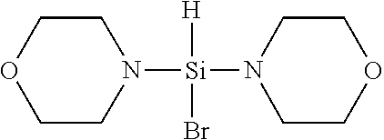
-
- The amino(bromo)silane precursor being:

-
- The amino(bromo)silane precursor being:

-
- x=0;
- y=3;
- z=1;
- The amino(bromo)silane precursor having the formula:

-
- R1 and R2 selected independently from C1-C6 alkyl, aryl, or hetero group;
- R1 and R2 selected independently from C1-C6 alkyl, aryl, or hetero group, provided that R1 and R2 do not equal iPr;
- The amino(bromo)silane precursor being:

-
- The amino(bromo)silane precursor being:

-
- The amino(bromo)silane precursor being:

-
- The amino(bromo)silane precursor being:

-
- The amino(bromo)silane precursor being:

-
- The amino(bromo)silane precursor being:

-
- The amino(bromo)silane precursor being:

-
- The amino(bromo)silane precursor being:

-
- The amino(bromo)silane precursor being:

-
- The amino(bromo)silane precursor being:

-
- The amino(bromo)silane precursor being:

-
- The amino(bromo)silane precursor being:

-
- The amino(bromo)silane precursor being:

-
- The amino(bromo)silane precursor being:

-
- The amino(bromo)silane precursor being:

-
- y=2;
- z=2;
- The amino(bromo)silane precursor having the formula:

-
- R1 and R2 selected independently from C1-C6 alkyl, aryl, or hetero group;
- The amino(bromo)silane precursor being:

-
- The amino(bromo)silane precursor being:

-
- The amino(bromo)silane precursor being:

-
- The amino(bromo)silane precursor being:

-
- The amino(bromo)silane precursor being:

-
- The amino(bromo)silane precursor being:

-
- The amino(bromo)silane precursor being:

-
- The amino(bromo)silane precursor being:

-
- The amino(bromo)silane precursor being:

-
- The amino(bromo)silane precursor being:

-
- The amino(bromo)silane precursor being:

-
- The amino(bromo)silane precursor being:

-
- The amino(bromo)silane precursor being:

-
- The amino(bromo)silane precursor being:

-
- The amino(bromo)silane precursor being:

-
- y=1;
- z=3;
- The amino(bromo)silane precursor having the formula:

-
- R1 and R2 selected independently from C1-C6 alkyl, aryl, or hetero group;
- The amino(bromo)silane precursor being:

-
- The amino(bromo)silane precursor being:

-
- The amino(bromo)silane precursor being:

-
- The amino(bromo)silane precursor being:

-
- The amino(bromo)silane precursor being:

-
- The amino(bromo)silane precursor being:

-
- The amino(bromo)silane precursor being:

-
- the Si-containing film forming composition comprising between approximately 95% w/w and approximately 100% w/w of the amino(bromo)silane precursor;
- the Si-containing film forming composition comprising between approximately 5% w/w and approximately 50% w/w of the amino(bromo)silane precursor;
- the Si-containing film forming composition comprising no water;
- the Si-containing film forming composition comprising between approximately 0% w/w and approximately 5% w/w impurities;
- the Si-containing film forming composition comprising between approximately 0.0% w/w and approximately 2.0% w/w impurities;
- the Si-containing film forming composition comprising between approximately 0.0% w/w and approximately 1.0% w/w impurities;
- the impurities including ammonium salts; alkylamines; dialkylamines; alkylimines; bromosilanes; aminosilanes; lithium, sodium, or potassium bromide; bromine; THF; ether; pentane; cyclohexane; heptanes; benzene; toluene; halogenated metal amino(bromo)silane precursors;
- the Si-containing film forming composition comprising between approximately 0 ppbw and approximately 1 ppmw metal impurities;
- the Si-containing film forming composition comprising between approximately 0 ppbw and approximately 500 ppbw metal impurities;
- the Si-containing film forming composition comprising between approximately 0 ppbw and approximately 100 ppbw Al;
- the Si-containing film forming composition comprising between approximately 0 ppbw and approximately 100 ppbw As;
- the Si-containing film forming composition comprising between approximately 0 ppbw and approximately 100 ppbw Ba;
- the Si-containing film forming composition comprising between approximately 0 ppbw and approximately 100 ppbw Be;
- the Si-containing film forming composition comprising between approximately 0 ppbw and approximately 100 ppbw Bi;
- the Si-containing film forming composition comprising between approximately 0 ppbw and approximately 100 ppbw Cd;
- the Si-containing film forming composition comprising between approximately 0 ppbw and approximately 100 ppbw Ca;
- the Si-containing film forming composition comprising between approximately 0 ppbw and approximately 100 ppbw Cr;
- the Si-containing film forming composition comprising between approximately 0 ppbw and approximately 100 ppbw Co;
- the Si-containing film forming composition comprising between approximately 0 ppbw and approximately 100 ppbw Cu;
- the Si-containing film forming composition comprising between approximately 0 ppbw and approximately 100 ppbw Ga;
- the Si-containing film forming composition comprising between approximately 0 ppbw and approximately 100 ppbw Ge;
- the Si-containing film forming composition comprising between approximately 0 ppbw and approximately 100 ppbw Hf;
- the Si-containing film forming composition comprising between approximately 0 ppbw and approximately 100 ppbw Zr;
- the Si-containing film forming composition comprising between approximately 0 ppbw and approximately 100 ppbw In;
- the Si-containing film forming composition comprising between approximately 0 ppbw and approximately 100 ppbw Fe;
- the Si-containing film forming composition comprising between approximately 0 ppbw and approximately 100 ppbw Pb;
- the Si-containing film forming composition comprising between approximately 0 ppbw and approximately 100 ppbw Li;
- the Si-containing film forming composition comprising between approximately 0 ppbw and approximately 100 ppbw Mg;
- the Si-containing film forming composition comprising between approximately 0 ppbw and approximately 100 ppbw Mn;
- the Si-containing film forming composition comprising between approximately 0 ppbw and approximately 100 ppbw W;
- the Si-containing film forming composition comprising between approximately 0 ppbw and approximately 100 ppbw Ni;
- the Si-containing film forming composition comprising between approximately 0 ppbw and approximately 100 ppbw K;
- the Si-containing film forming composition comprising between approximately 0 ppbw and approximately 100 ppbw Na;
- the Si-containing film forming composition comprising between approximately 0 ppbw and approximately 100 ppbw Sr;
- the Si-containing film forming composition comprising between approximately 0 ppbw and approximately 100 ppbw Th;
- the Si-containing film forming composition comprising between approximately 0 ppbw and approximately 100 ppbw Sn;
- the Si-containing film forming composition comprising between approximately 0 ppbw and approximately 100 ppbw Ti;
- the Si-containing film forming composition comprising between approximately 0 ppbw and approximately 100 ppbw U;
- the Si-containing film forming composition comprising between approximately 0 ppbw and approximately 100 ppbw V;
- the Si-containing film forming composition comprising between approximately 0 ppbw and approximately 100 ppbw Zn;
- the Si-containing film forming composition comprising between approximately 0 ppmw and approximately 100 ppmw Cl; and
- the Si-containing film forming composition comprising between approximately 0 ppmw and approximately 100 ppmw I.
-
- The disclosed Si-containing film forming compositions comprising an amino(bromo)silane precursor selected from SiH2Br(N(Et)2), SiH2Br(N(iPr)2), SiH2Br(N(iBu)2) or SiBr(NMe2)3;
- The disclosed amino(bromo)silane precursor being SiH2Br(N(Et)2);
- The disclosed amino(bromo)silane precursor being SiH2Br(N(i Pr)2);
- The disclosed amino(bromo)silane precursor being SiH2Br(N(iBu)2);
- The disclosed amino(bromo)silane precursor being SiBr(NMe2)3;
- introducing into the reactor a vapor comprising a second precursor;
- an element of the second precursor being selected from the group consisting of group 2, group 13, group 14, transition metal, lanthanides, and combinations thereof;
- the element of the second precursor being selected from Mg, Ca, Sr, Ba, Zr, Hf, Ti, Nb, Ta, Al, Si, Ge, Y, or lanthanides;
- introducing a reactant into the reactor;
- the reactant being selected from the group consisting of O2, O3, H2O, H2O2, NO, NO2, a carboxylic acid, radicals thereof, and combinations thereof;
- the reactant being plasma treated oxygen or ozone;
- the reactant being ozone;
- the reactant being selected from the group consisting of H2, NH3, (SiH3)3N, hydridosilanes (such as SiH4, Si2H6, Si3H8, Si4H10, Si5H10, Si6H12), chlorosilanes and chloropolysilanes (such as SiHCl3, SiH2Cl2, SiH3Cl, Si2Cl6, Si2HCl5, Si3Cl8), alkysilanes (such as Me2SiH2, Et2SiH2, MeSiH3, EtSiH3), hydrazines (such as N2H4, MeHNNH2, MeHNNHMe), organic amines (such as NMeH2, NEtH2, NMe2H, NEt2H, NMe3, NEt3, (SiMe3)2NH), pyrazoline, pyridine, B-containing molecules (such as B2H6, 9-borabicylo[3,3,1]none, trimethylboron, triethylboron, borazine), alkyl metals (such as trimethylaluminum, triethylaluminum, dimethylzinc, diethylzinc), radical species thereof, and mixtures thereof;
- the reactant being selected from the group consisting of H2, NH3, SiH4, Si2H6, Si3H8, SiH2Me2, SiH2Et2, N(SiH3)3, hydrogen radicals thereof, and mixtures thereof;
- the reactant being selected from the group consisting of NH3, N2H4, N(SiH3)3, N(CH3)H2, N(C2H5)H2, N(CH3)2H, N(C2H5)2H, N(CH3)3, N(C2H5)3, (SiMe3)2NH, (CH3)HNNH2, (CH3)2NNH2, nitrogen-containing radical species thereof, and mixtures thereof;
- the reactant being HCDS or PCDS;
- the vapor deposition method being a CVD process;
- the vapor deposition method being an ALD process;
- the vapor deposition method being a spatial ALD process;
- the Si-containing layer being a silicon oxide layer;
- the Si-containing layer being Si;
- the Si-containing layer being SiO2;
- the Si-containing layer being SiN;
- the Si-containing layer being SiON;
- the Si-containing layer being SiCN; and
- the Si-containing layer being SiCOH.
-
- the Si-containing film forming composition having a total concentration of metal contaminants of less than 10 ppmw;
- an end of the inlet conduit end located above a surface of the Si-containing film forming composition and an end of the outlet conduit located below the surface of the Si-containing film forming composition;
- an end of the inlet conduit end located below a surface of the Si-containing film forming composition and an end of the outlet conduit located above the surface of the Si-containing film forming composition;
- further comprising a diaphragm valve on the inlet and the outlet;
- further comprising one or more barrier layers on an interior surface of the canister;
- further comprising one to four barrier layers on an interior surface of the canister;
- further comprising one or two barrier layers on an interior surface of the canister;
- each barrier layer comprising a silicon oxide layer, a silicon nitride layer, silicon oxynitride layer, a silicon carbonitride, silicon oxycarbonitride layer, or combinations thereof;
- wherein each barrier layer is 5 to 1000 nm in thickness;
- wherein each barrier layer is 50 to 500 nm in thickness;
- the Si-containing film forming composition being SiH2Br(N(Et)2), SiH2Br(N(iPr)2), SiH2Br(N(iBu)2), or SiBr(NMe2)3.
| TABLE 1 | |
| a or an | One or more than one |
| Approximately or | ±10% of the value stated |
| about | |
| LCD-TFT | liquid-crystal display |
| TFT | thin-film transistor |
| MIM | Metal-insulator-metal |
| DRAM | dynamic random-access memory |
| FeRam | Ferroelectric random-access memory |
| CVD | chemical vapor deposition |
| LPCVD | low pressure chemical vapor deposition |
| PCVD | pulsed chemical vapor deposition |
| SACVD | sub-atmospheric chemical vapor deposition |
| PECVD | plasma enhanced chemical vapor deposition |
| APCVD | atmospheric pressure chemical vapor deposition |
| HWCVD | hot-wire chemical vapor deposition |
| Flowable PECVD | flowable plasma enhanced chemical vapor deposition |
| MOCVD | metal organic chemical vapor deposition |
| ALD | atomic layer deposition |
| spatial ALD | spatial atomic layer deposition |
| HWALD | hot-wire atomic layer deposition |
| PEALD | plasma enhanced atomic layer deposition |
| DSSD | dual silicone source deposition |
| sccm | standard cubic centimeters per minute |
| MP | melting point |
| TGA | thermogravimetric analysis |
| SDTA | simultaneous differential thermal analysis |
| GCMS | gas chromatography-mass spectrometry |
| SRO | strontium ruthenium oxide |
| HCDS | Hexachlorodisilane |
| PCDS | Pentachlorodisilane |
| LAH | lithium aluminum hydride |
| TriDMAS or | Tris(dimethylamino)silane or SiH(NMe2)3 |
| TDMAS | |
| BDMAS | Bis(dimethylamino)silane or SiH2(NMe2)2 |
| BDEAS | Bis(diethylamino)silane or SiH2(NEt2)2 |
| TDEAS | Tris(diethylamino)silane or SiH(NEt2)3 |
| TEMAS | Tris(ethylmethylamino)silane or SiH(NEtMe)3 |
| TMA | trimethyl aluminum or AIMe3 |
| TBTDET | (tert-butylimido)tris(diethylamido) tantalum or |
| Ta(═NtBu)(NEt2)3 | |
| TAT-DMAE | tantalum tetraethoxide dimethylaminoethoxide or |
| Ta(OEt)4(OCH2CH2NMe2) | |
| PET | polyethylene terephthalate |
| TBTDEN | (tert-butylimido)bis(dimethylamino)niobium or |
| Nb(═NtBu)(NMe2)2 | |
| PEN | polyethylene naphthalate |
| Ln(tmhd)3 | lanthanide (2,2,6,6-tetramethyl-3,5-heptanedione)3 |
| alkyl group | saturated functional groups containing exclusively |
| carbon and hydrogen atoms, including | |
| linear, branched, or cyclic alkyl groups | |
| aryl | aromatic ring compounds where one hydrogen atom |
| has been removed from the ring | |
| Hetero | a functional group containing C and a second non-H |
| element, such as S or O | |
| heterocycle | cyclic compounds that has atoms of at least two |
| different elements as members of its ring | |
| Me | Methyl |
| Et | Ethyl |
| Pr | Propyl, including iPr and nPr |
| iPr | iso-Propyl |
| nPr | n-Propyl |
| Bu | Butyl, including iBu, sBu, and tBu |
| iBu | iso-Butyl |
| sBu | Sec-Butyl |
| tBu | Tert-Butyl |
SiHxBry(NR1R2)z (I)
wherein x+y+z=4; x=0, 1 or 2; y=1, 2 or 3; z=1, 2, or 3; R1 and R2 selected independently from C1-C6 alkyl, aryl, or hetero group; and R1 and R2 may be joined to form a cyclic nitrogen-containing heterocycle.
-
- liquid at room temperature or having a melting point lower than 50° C.;
- thermally stable to enable proper distribution (gas phase or direct liquid injection) without particles generation;
- suitable reactivity with the substrate to permit a wide self-limited ALD window, allowing deposition of a variety of Si-containing films, such as SiGe or SiSn, by using one or a combination of reactants (selected from the group comprising of H2, NH3, O2, H2O, O3, SiH4, Si2H6, Si3H8, SiH(NMe2)3 (TriDMAS or TDMAS), SiH2(NMe2)2 (BDMAS), SiH2(N(Et)2)2 (BDEAS), SiH(N(Et)2)3(TDEAS), SiH(NEtMe)3 (TEMAS), (SiH3)3N, (SiH3)2O, (GeH3)2, Bu4Ge, GeMe4, GeEt4, Ge(allyl), (Ge(NMe2)4, Ge(N(SiMe3)2)4, GeCl2-dioxane, GeBr2, GeCl4, Ge(OMe)4, Ge(OEt)4, Sn(OtBu)4, SnI4, SnMe4, Sn(AcAc)2, Sn(NMe2)4, Sn(NEt2)4, Sn(N(SiMe3)2)2, an aluminum-containing precursor such as trimethyl aluminum (TMA), (tert-butylimido)tris(diethylamido) tantalum (TBTDET), tantalum tetraethoxide dimethylaminoethoxide (TAT-DMAE), polyethylene terephthalate (PET), (tert-butylimido)bis(dimethylamino)niobium (TBTDEN), polyethylene naphthalate (PEN), lanthanide-containing precursors such as Ln(tmhd)3 (lanthanide (2,2,6,6-tetramethyl-3,5-heptanedione)3)).

wherein R1 and R2 selected independently from C1-C6 alkyl, aryl, or hetero group and R1 and R2 may be joined to form a cyclic nitrogen-containing heterocycle.


wherein R1 and R2 selected independently from C1-C6 alkyl, aryl, or hetero group and R1 and R2 may be joined to form a cyclic nitrogen-containing heterocycle.


wherein R1 and R2 selected independently from C1-C6 alkyl, aryl, or hetero group and R1 and R2 may be joined to form a cyclic nitrogen-containing heterocycle.


wherein R1 and R2 selected independently from C3-C6 alkyl, aryl, or hetero group and R1 and R2 may be joined to form a cyclic nitrogen-containing heterocycle.


wherein R1 and R2 selected independently from C1-C6 alkyl, aryl, or hetero group and R1 and R2 may be joined to form a cyclic nitrogen-containing heterocycle.


wherein R1 and R2 selected independently from C1-C6 alkyl, aryl, or hetero group and R1 and R2 may be joined to form a cyclic nitrogen-containing heterocycle.

Claims (20)
SiHxBry(NR1R2)4−x−y


Priority Applications (1)
| Application Number | Priority Date | Filing Date | Title |
|---|---|---|---|
| US14/984,908 US10053775B2 (en) | 2015-12-30 | 2015-12-30 | Methods of using amino(bromo)silane precursors for ALD/CVD silicon-containing film applications |
Applications Claiming Priority (1)
| Application Number | Priority Date | Filing Date | Title |
|---|---|---|---|
| US14/984,908 US10053775B2 (en) | 2015-12-30 | 2015-12-30 | Methods of using amino(bromo)silane precursors for ALD/CVD silicon-containing film applications |
Publications (2)
| Publication Number | Publication Date |
|---|---|
| US20160108064A1 US20160108064A1 (en) | 2016-04-21 |
| US10053775B2 true US10053775B2 (en) | 2018-08-21 |
Family
ID=55748502
Family Applications (1)
| Application Number | Title | Priority Date | Filing Date |
|---|---|---|---|
| US14/984,908 Active 2036-07-30 US10053775B2 (en) | 2015-12-30 | 2015-12-30 | Methods of using amino(bromo)silane precursors for ALD/CVD silicon-containing film applications |
Country Status (1)
| Country | Link |
|---|---|
| US (1) | US10053775B2 (en) |
Families Citing this family (5)
| Publication number | Priority date | Publication date | Assignee | Title |
|---|---|---|---|---|
| KR20200136386A (en) * | 2018-03-29 | 2020-12-07 | 스미토모 세이카 가부시키가이샤 | An aminosilane compound, and a composition for forming a silicone-containing film containing the aminosilane compound |
| US20200040454A1 (en) * | 2018-08-06 | 2020-02-06 | Lam Research Corporation | Method to increase deposition rate of ald process |
| US20210225634A1 (en) * | 2020-01-17 | 2021-07-22 | Asm Ip Holding B.V. | FORMATION OF SiCN THIN FILMS |
| US20210225633A1 (en) * | 2020-01-17 | 2021-07-22 | Asm Ip Holding B.V. | FORMATION OF SiOCN THIN FILMS |
| KR102364476B1 (en) * | 2020-05-08 | 2022-02-18 | 주식회사 한솔케미칼 | Silicon precursor and fabrication method of silicon-containing thin film using the same |
Citations (22)
| Publication number | Priority date | Publication date | Assignee | Title |
|---|---|---|---|---|
| JP2006096675A (en) | 2004-09-28 | 2006-04-13 | L'air Liquide Sa Pour L'etude & L'exploitation Des Procede S Georges Claude | New amino-disilane and method for forming silicon carbonitride film |
| WO2006059187A1 (en) | 2004-12-02 | 2006-06-08 | L'air Liquide, Societe Anonyme Pour L'etude Et L'exploitation Des Procedes Georges Claude | Liquid precursor refill system |
| US7125582B2 (en) | 2003-07-30 | 2006-10-24 | Intel Corporation | Low-temperature silicon nitride deposition |
| US7402243B2 (en) | 2004-09-10 | 2008-07-22 | Dionex Corporation | Organosilanes and substrate bonded with same |
| WO2009087609A2 (en) | 2008-01-10 | 2009-07-16 | L'air Liquide-Societe Anonyme Pour L'etude Et L'exploitation Des Procedes Georges Claude | Solid precursor sublimator |
| US20090197411A1 (en) * | 2008-02-01 | 2009-08-06 | Christian Dussarrat | New metal precursors containing beta-diketiminato ligands |
| US20100055442A1 (en) * | 2008-09-03 | 2010-03-04 | International Business Machines Corporation | METHOD OF PE-ALD OF SiNxCy AND INTEGRATION OF LINER MATERIALS ON POROUS LOW K SUBSTRATES |
| WO2011123792A2 (en) | 2010-04-01 | 2011-10-06 | L'air Liquide, Societe Anonyme Pour L'etude Et L'exploitation Des Procedes Georges Claude | Metal nitride containing film deposition using combination of amino-metal and halogenated metal precursors |
| US20120021127A1 (en) | 2009-03-19 | 2012-01-26 | Adeka Corporation | Material for chemical vapor deposition and process for forming silicon-containing thin film using same |
| US20120178264A1 (en) * | 2010-12-21 | 2012-07-12 | Tokyo Electron Limited | Method and apparatus for forming silicon nitride film |
| US20120277457A1 (en) | 2010-10-12 | 2012-11-01 | Air Products And Chemicals, Inc. | Aminosilanes and methods for making same |
| WO2012167060A2 (en) | 2011-06-03 | 2012-12-06 | Air Products And Chemicals, Inc. | Compositions and processes for depositing carbon-doped silicon-containing films |
| US20130078392A1 (en) | 2011-09-27 | 2013-03-28 | Air Products And Chemicals, Inc. | Halogenated organoaminosilane precursors and methods for depositing films comprising same |
| US20130129940A1 (en) * | 2011-05-24 | 2013-05-23 | Air Products And Chemicals, Inc. | Organoaminosilane precursors and methods for making and using same |
| US20130323435A1 (en) | 2012-06-01 | 2013-12-05 | Air Products And Chemicals, Inc. | Organoaminodisilane precursors and methods for depositing films comprising same |
| US20130319290A1 (en) | 2012-06-01 | 2013-12-05 | Air Products And Chemicals, Inc. | Organoaminodisilane precursors and methods for depositing films comprising same |
| US20140051264A1 (en) | 2012-03-05 | 2014-02-20 | Applied Materials, Inc. | Flowable films using alternative silicon precursors |
| US20140273531A1 (en) | 2013-03-14 | 2014-09-18 | Asm Ip Holding B.V. | Si PRECURSORS FOR DEPOSITION OF SiN AT LOW TEMPERATURES |
| US20140273528A1 (en) | 2013-03-14 | 2014-09-18 | Asm Ip Holding B.V. | Si PRECURSORS FOR DEPOSITION OF SiN AT LOW TEMPERATURES |
| US20140273477A1 (en) | 2013-03-14 | 2014-09-18 | Asm Ip Holding B.V. | Si PRECURSORS FOR DEPOSITION OF SiN AT LOW TEMPERATURES |
| US9233990B2 (en) | 2014-02-28 | 2016-01-12 | Air Products And Chemicals, Inc. | Organoaminosilanes and methods for making same |
| US20160115593A1 (en) * | 2015-12-30 | 2016-04-28 | American Air Liquide, Inc. | Amino(iodo)silane precursors for ald/cvd silicon-containing film applications and methods of using the same |
-
2015
- 2015-12-30 US US14/984,908 patent/US10053775B2/en active Active
Patent Citations (22)
| Publication number | Priority date | Publication date | Assignee | Title |
|---|---|---|---|---|
| US7125582B2 (en) | 2003-07-30 | 2006-10-24 | Intel Corporation | Low-temperature silicon nitride deposition |
| US7402243B2 (en) | 2004-09-10 | 2008-07-22 | Dionex Corporation | Organosilanes and substrate bonded with same |
| JP2006096675A (en) | 2004-09-28 | 2006-04-13 | L'air Liquide Sa Pour L'etude & L'exploitation Des Procede S Georges Claude | New amino-disilane and method for forming silicon carbonitride film |
| WO2006059187A1 (en) | 2004-12-02 | 2006-06-08 | L'air Liquide, Societe Anonyme Pour L'etude Et L'exploitation Des Procedes Georges Claude | Liquid precursor refill system |
| WO2009087609A2 (en) | 2008-01-10 | 2009-07-16 | L'air Liquide-Societe Anonyme Pour L'etude Et L'exploitation Des Procedes Georges Claude | Solid precursor sublimator |
| US20090197411A1 (en) * | 2008-02-01 | 2009-08-06 | Christian Dussarrat | New metal precursors containing beta-diketiminato ligands |
| US20100055442A1 (en) * | 2008-09-03 | 2010-03-04 | International Business Machines Corporation | METHOD OF PE-ALD OF SiNxCy AND INTEGRATION OF LINER MATERIALS ON POROUS LOW K SUBSTRATES |
| US20120021127A1 (en) | 2009-03-19 | 2012-01-26 | Adeka Corporation | Material for chemical vapor deposition and process for forming silicon-containing thin film using same |
| WO2011123792A2 (en) | 2010-04-01 | 2011-10-06 | L'air Liquide, Societe Anonyme Pour L'etude Et L'exploitation Des Procedes Georges Claude | Metal nitride containing film deposition using combination of amino-metal and halogenated metal precursors |
| US20120277457A1 (en) | 2010-10-12 | 2012-11-01 | Air Products And Chemicals, Inc. | Aminosilanes and methods for making same |
| US20120178264A1 (en) * | 2010-12-21 | 2012-07-12 | Tokyo Electron Limited | Method and apparatus for forming silicon nitride film |
| US20130129940A1 (en) * | 2011-05-24 | 2013-05-23 | Air Products And Chemicals, Inc. | Organoaminosilane precursors and methods for making and using same |
| WO2012167060A2 (en) | 2011-06-03 | 2012-12-06 | Air Products And Chemicals, Inc. | Compositions and processes for depositing carbon-doped silicon-containing films |
| US20130078392A1 (en) | 2011-09-27 | 2013-03-28 | Air Products And Chemicals, Inc. | Halogenated organoaminosilane precursors and methods for depositing films comprising same |
| US20140051264A1 (en) | 2012-03-05 | 2014-02-20 | Applied Materials, Inc. | Flowable films using alternative silicon precursors |
| US20130323435A1 (en) | 2012-06-01 | 2013-12-05 | Air Products And Chemicals, Inc. | Organoaminodisilane precursors and methods for depositing films comprising same |
| US20130319290A1 (en) | 2012-06-01 | 2013-12-05 | Air Products And Chemicals, Inc. | Organoaminodisilane precursors and methods for depositing films comprising same |
| US20140273531A1 (en) | 2013-03-14 | 2014-09-18 | Asm Ip Holding B.V. | Si PRECURSORS FOR DEPOSITION OF SiN AT LOW TEMPERATURES |
| US20140273528A1 (en) | 2013-03-14 | 2014-09-18 | Asm Ip Holding B.V. | Si PRECURSORS FOR DEPOSITION OF SiN AT LOW TEMPERATURES |
| US20140273477A1 (en) | 2013-03-14 | 2014-09-18 | Asm Ip Holding B.V. | Si PRECURSORS FOR DEPOSITION OF SiN AT LOW TEMPERATURES |
| US9233990B2 (en) | 2014-02-28 | 2016-01-12 | Air Products And Chemicals, Inc. | Organoaminosilanes and methods for making same |
| US20160115593A1 (en) * | 2015-12-30 | 2016-04-28 | American Air Liquide, Inc. | Amino(iodo)silane precursors for ald/cvd silicon-containing film applications and methods of using the same |
Non-Patent Citations (12)
Also Published As
| Publication number | Publication date |
|---|---|
| US20160108064A1 (en) | 2016-04-21 |
Similar Documents
| Publication | Publication Date | Title |
|---|---|---|
| US11699584B2 (en) | Si-containing film forming precursors and methods of using the same | |
| US9822132B2 (en) | Hexacoordinate silicon-containing precursors for ALD/CVD silicon-containing film applications | |
| US20160314962A1 (en) | Cyclic organoaminosilane precursors for forming silicon-containing films and methods of using the same | |
| US9777373B2 (en) | Amino(iodo)silane precursors for ALD/CVD silicon-containing film applications and methods of using the same | |
| US9938303B2 (en) | Organosilane precursors for ALD/CVD silicon-containing film applications | |
| US10053775B2 (en) | Methods of using amino(bromo)silane precursors for ALD/CVD silicon-containing film applications | |
| US9382268B1 (en) | Sulfur containing organosilane precursors for ALD/CVD silicon-containing film applications | |
| US9719167B2 (en) | Cobalt-containing film forming compositions, their synthesis, and use in film deposition | |
| EP3307744B1 (en) | Vapor deposition processes for forming silicon- and oxygen-containing thin films | |
| US10011903B2 (en) | Manganese-containing film forming compositions, their synthesis, and use in film deposition | |
| US10570513B2 (en) | Organosilane precursors for ALD/CVD silicon-containing film applications and methods of using the same | |
| US10006122B2 (en) | Organodisilane precursors for ALD/CVD silicon-containing film applications | |
| US9738971B2 (en) | Vapor deposition methods to form group 8-containing films | |
| EP3307745B1 (en) | Vapor deposition processes for forming silicon- and nitrogen-containing thin films | |
| WO2017127044A1 (en) | Si-containing film forming compositions for ald/cvd of silicon-containing films |
Legal Events
| Date | Code | Title | Description |
|---|---|---|---|
| AS | Assignment |
Owner name: AMERICAN AIR LIQUIDE, INC., CALIFORNIA Free format text: ASSIGNMENT OF ASSIGNORS INTEREST;ASSIGNORS:KUCHENBEISER, GLENN;PALLEM, VENKATESWARA R.;REEL/FRAME:039439/0960 Effective date: 20160801 |
|
| AS | Assignment |
Owner name: L'AIR LIQUIDE, SOCIETE ANONYME POUR L'ETUDE ET L'E Free format text: ASSIGNMENT OF ASSIGNORS INTEREST;ASSIGNORS:BLASCO, NICOLAS;GIRARD, JEAN-MARC;REEL/FRAME:039495/0893 Effective date: 20160818 |
|
| STCF | Information on status: patent grant |
Free format text: PATENTED CASE |
|
| MAFP | Maintenance fee payment |
Free format text: PAYMENT OF MAINTENANCE FEE, 4TH YEAR, LARGE ENTITY (ORIGINAL EVENT CODE: M1551); ENTITY STATUS OF PATENT OWNER: LARGE ENTITY Year of fee payment: 4 |