WO2010103745A1 - 半導体封止用樹脂組成物及び半導体装置 - Google Patents
半導体封止用樹脂組成物及び半導体装置 Download PDFInfo
- Publication number
- WO2010103745A1 WO2010103745A1 PCT/JP2010/001410 JP2010001410W WO2010103745A1 WO 2010103745 A1 WO2010103745 A1 WO 2010103745A1 JP 2010001410 W JP2010001410 W JP 2010001410W WO 2010103745 A1 WO2010103745 A1 WO 2010103745A1
- Authority
- WO
- WIPO (PCT)
- Prior art keywords
- resin
- semiconductor
- resin composition
- general formula
- epoxy resin
- Prior art date
- Legal status (The legal status is an assumption and is not a legal conclusion. Google has not performed a legal analysis and makes no representation as to the accuracy of the status listed.)
- Ceased
Links
- 0 C[P+](C)(*)Cc1c(*)c(O)c(*)c(*)c1O Chemical compound C[P+](C)(*)Cc1c(*)c(O)c(*)c(*)c1O 0.000 description 3
Images




Classifications
-
- H—ELECTRICITY
- H10—SEMICONDUCTOR DEVICES; ELECTRIC SOLID-STATE DEVICES NOT OTHERWISE PROVIDED FOR
- H10W—GENERIC PACKAGES, INTERCONNECTIONS, CONNECTORS OR OTHER CONSTRUCTIONAL DETAILS OF DEVICES COVERED BY CLASS H10
- H10W74/00—Encapsulations, e.g. protective coatings
- H10W74/10—Encapsulations, e.g. protective coatings characterised by their shape or disposition
- H10W74/111—Encapsulations, e.g. protective coatings characterised by their shape or disposition the semiconductor body being completely enclosed
- H10W74/114—Encapsulations, e.g. protective coatings characterised by their shape or disposition the semiconductor body being completely enclosed by a substrate and the encapsulations
- H10W74/117—Encapsulations, e.g. protective coatings characterised by their shape or disposition the semiconductor body being completely enclosed by a substrate and the encapsulations the substrate having spherical bumps for external connection
-
- C—CHEMISTRY; METALLURGY
- C08—ORGANIC MACROMOLECULAR COMPOUNDS; THEIR PREPARATION OR CHEMICAL WORKING-UP; COMPOSITIONS BASED THEREON
- C08G—MACROMOLECULAR COMPOUNDS OBTAINED OTHERWISE THAN BY REACTIONS ONLY INVOLVING UNSATURATED CARBON-TO-CARBON BONDS
- C08G59/00—Polycondensates containing more than one epoxy group per molecule; Macromolecules obtained by polymerising compounds containing more than one epoxy group per molecule using curing agents or catalysts which react with the epoxy groups
- C08G59/18—Macromolecules obtained by polymerising compounds containing more than one epoxy group per molecule using curing agents or catalysts which react with the epoxy groups ; e.g. general methods of curing
- C08G59/40—Macromolecules obtained by polymerising compounds containing more than one epoxy group per molecule using curing agents or catalysts which react with the epoxy groups ; e.g. general methods of curing characterised by the curing agents used
- C08G59/62—Alcohols or phenols
-
- C—CHEMISTRY; METALLURGY
- C08—ORGANIC MACROMOLECULAR COMPOUNDS; THEIR PREPARATION OR CHEMICAL WORKING-UP; COMPOSITIONS BASED THEREON
- C08G—MACROMOLECULAR COMPOUNDS OBTAINED OTHERWISE THAN BY REACTIONS ONLY INVOLVING UNSATURATED CARBON-TO-CARBON BONDS
- C08G59/00—Polycondensates containing more than one epoxy group per molecule; Macromolecules obtained by polymerising compounds containing more than one epoxy group per molecule using curing agents or catalysts which react with the epoxy groups
- C08G59/18—Macromolecules obtained by polymerising compounds containing more than one epoxy group per molecule using curing agents or catalysts which react with the epoxy groups ; e.g. general methods of curing
- C08G59/20—Macromolecules obtained by polymerising compounds containing more than one epoxy group per molecule using curing agents or catalysts which react with the epoxy groups ; e.g. general methods of curing characterised by the epoxy compounds used
- C08G59/22—Di-epoxy compounds
- C08G59/24—Di-epoxy compounds carbocyclic
- C08G59/245—Di-epoxy compounds carbocyclic aromatic
-
- C—CHEMISTRY; METALLURGY
- C08—ORGANIC MACROMOLECULAR COMPOUNDS; THEIR PREPARATION OR CHEMICAL WORKING-UP; COMPOSITIONS BASED THEREON
- C08G—MACROMOLECULAR COMPOUNDS OBTAINED OTHERWISE THAN BY REACTIONS ONLY INVOLVING UNSATURATED CARBON-TO-CARBON BONDS
- C08G59/00—Polycondensates containing more than one epoxy group per molecule; Macromolecules obtained by polymerising compounds containing more than one epoxy group per molecule using curing agents or catalysts which react with the epoxy groups
- C08G59/18—Macromolecules obtained by polymerising compounds containing more than one epoxy group per molecule using curing agents or catalysts which react with the epoxy groups ; e.g. general methods of curing
- C08G59/40—Macromolecules obtained by polymerising compounds containing more than one epoxy group per molecule using curing agents or catalysts which react with the epoxy groups ; e.g. general methods of curing characterised by the curing agents used
- C08G59/62—Alcohols or phenols
- C08G59/621—Phenols
-
- C—CHEMISTRY; METALLURGY
- C08—ORGANIC MACROMOLECULAR COMPOUNDS; THEIR PREPARATION OR CHEMICAL WORKING-UP; COMPOSITIONS BASED THEREON
- C08L—COMPOSITIONS OF MACROMOLECULAR COMPOUNDS
- C08L63/00—Compositions of epoxy resins; Compositions of derivatives of epoxy resins
-
- H—ELECTRICITY
- H10—SEMICONDUCTOR DEVICES; ELECTRIC SOLID-STATE DEVICES NOT OTHERWISE PROVIDED FOR
- H10W—GENERIC PACKAGES, INTERCONNECTIONS, CONNECTORS OR OTHER CONSTRUCTIONAL DETAILS OF DEVICES COVERED BY CLASS H10
- H10W74/00—Encapsulations, e.g. protective coatings
- H10W74/01—Manufacture or treatment
- H10W74/016—Manufacture or treatment using moulds
-
- H—ELECTRICITY
- H10—SEMICONDUCTOR DEVICES; ELECTRIC SOLID-STATE DEVICES NOT OTHERWISE PROVIDED FOR
- H10W—GENERIC PACKAGES, INTERCONNECTIONS, CONNECTORS OR OTHER CONSTRUCTIONAL DETAILS OF DEVICES COVERED BY CLASS H10
- H10W74/00—Encapsulations, e.g. protective coatings
- H10W74/10—Encapsulations, e.g. protective coatings characterised by their shape or disposition
- H10W74/111—Encapsulations, e.g. protective coatings characterised by their shape or disposition the semiconductor body being completely enclosed
-
- H—ELECTRICITY
- H10—SEMICONDUCTOR DEVICES; ELECTRIC SOLID-STATE DEVICES NOT OTHERWISE PROVIDED FOR
- H10W—GENERIC PACKAGES, INTERCONNECTIONS, CONNECTORS OR OTHER CONSTRUCTIONAL DETAILS OF DEVICES COVERED BY CLASS H10
- H10W74/00—Encapsulations, e.g. protective coatings
- H10W74/40—Encapsulations, e.g. protective coatings characterised by their materials
- H10W74/47—Encapsulations, e.g. protective coatings characterised by their materials comprising organic materials, e.g. plastics or resins
- H10W74/473—Encapsulations, e.g. protective coatings characterised by their materials comprising organic materials, e.g. plastics or resins containing a filler
-
- H—ELECTRICITY
- H10—SEMICONDUCTOR DEVICES; ELECTRIC SOLID-STATE DEVICES NOT OTHERWISE PROVIDED FOR
- H10W—GENERIC PACKAGES, INTERCONNECTIONS, CONNECTORS OR OTHER CONSTRUCTIONAL DETAILS OF DEVICES COVERED BY CLASS H10
- H10W70/00—Package substrates; Interposers; Redistribution layers [RDL]
- H10W70/40—Leadframes
- H10W70/411—Chip-supporting parts, e.g. die pads
- H10W70/417—Bonding materials between chips and die pads
-
- H—ELECTRICITY
- H10—SEMICONDUCTOR DEVICES; ELECTRIC SOLID-STATE DEVICES NOT OTHERWISE PROVIDED FOR
- H10W—GENERIC PACKAGES, INTERCONNECTIONS, CONNECTORS OR OTHER CONSTRUCTIONAL DETAILS OF DEVICES COVERED BY CLASS H10
- H10W72/00—Interconnections or connectors in packages
- H10W72/50—Bond wires
- H10W72/551—Materials of bond wires
- H10W72/552—Materials of bond wires comprising metals or metalloids, e.g. silver
-
- H—ELECTRICITY
- H10—SEMICONDUCTOR DEVICES; ELECTRIC SOLID-STATE DEVICES NOT OTHERWISE PROVIDED FOR
- H10W—GENERIC PACKAGES, INTERCONNECTIONS, CONNECTORS OR OTHER CONSTRUCTIONAL DETAILS OF DEVICES COVERED BY CLASS H10
- H10W72/00—Interconnections or connectors in packages
- H10W72/50—Bond wires
- H10W72/551—Materials of bond wires
- H10W72/552—Materials of bond wires comprising metals or metalloids, e.g. silver
- H10W72/5522—Materials of bond wires comprising metals or metalloids, e.g. silver comprising gold [Au]
-
- H—ELECTRICITY
- H10—SEMICONDUCTOR DEVICES; ELECTRIC SOLID-STATE DEVICES NOT OTHERWISE PROVIDED FOR
- H10W—GENERIC PACKAGES, INTERCONNECTIONS, CONNECTORS OR OTHER CONSTRUCTIONAL DETAILS OF DEVICES COVERED BY CLASS H10
- H10W72/00—Interconnections or connectors in packages
- H10W72/851—Dispositions of multiple connectors or interconnections
- H10W72/874—On different surfaces
- H10W72/884—Die-attach connectors and bond wires
-
- H—ELECTRICITY
- H10—SEMICONDUCTOR DEVICES; ELECTRIC SOLID-STATE DEVICES NOT OTHERWISE PROVIDED FOR
- H10W—GENERIC PACKAGES, INTERCONNECTIONS, CONNECTORS OR OTHER CONSTRUCTIONAL DETAILS OF DEVICES COVERED BY CLASS H10
- H10W74/00—Encapsulations, e.g. protective coatings
-
- H—ELECTRICITY
- H10—SEMICONDUCTOR DEVICES; ELECTRIC SOLID-STATE DEVICES NOT OTHERWISE PROVIDED FOR
- H10W—GENERIC PACKAGES, INTERCONNECTIONS, CONNECTORS OR OTHER CONSTRUCTIONAL DETAILS OF DEVICES COVERED BY CLASS H10
- H10W90/00—Package configurations
- H10W90/701—Package configurations characterised by the relative positions of pads or connectors relative to package parts
-
- H—ELECTRICITY
- H10—SEMICONDUCTOR DEVICES; ELECTRIC SOLID-STATE DEVICES NOT OTHERWISE PROVIDED FOR
- H10W—GENERIC PACKAGES, INTERCONNECTIONS, CONNECTORS OR OTHER CONSTRUCTIONAL DETAILS OF DEVICES COVERED BY CLASS H10
- H10W90/00—Package configurations
- H10W90/701—Package configurations characterised by the relative positions of pads or connectors relative to package parts
- H10W90/731—Package configurations characterised by the relative positions of pads or connectors relative to package parts of die-attach connectors
- H10W90/734—Package configurations characterised by the relative positions of pads or connectors relative to package parts of die-attach connectors between a chip and a stacked insulating package substrate, interposer or RDL
-
- H—ELECTRICITY
- H10—SEMICONDUCTOR DEVICES; ELECTRIC SOLID-STATE DEVICES NOT OTHERWISE PROVIDED FOR
- H10W—GENERIC PACKAGES, INTERCONNECTIONS, CONNECTORS OR OTHER CONSTRUCTIONAL DETAILS OF DEVICES COVERED BY CLASS H10
- H10W90/00—Package configurations
- H10W90/701—Package configurations characterised by the relative positions of pads or connectors relative to package parts
- H10W90/731—Package configurations characterised by the relative positions of pads or connectors relative to package parts of die-attach connectors
- H10W90/736—Package configurations characterised by the relative positions of pads or connectors relative to package parts of die-attach connectors between a chip and a stacked lead frame, conducting package substrate or heat sink
-
- H—ELECTRICITY
- H10—SEMICONDUCTOR DEVICES; ELECTRIC SOLID-STATE DEVICES NOT OTHERWISE PROVIDED FOR
- H10W—GENERIC PACKAGES, INTERCONNECTIONS, CONNECTORS OR OTHER CONSTRUCTIONAL DETAILS OF DEVICES COVERED BY CLASS H10
- H10W90/00—Package configurations
- H10W90/701—Package configurations characterised by the relative positions of pads or connectors relative to package parts
- H10W90/751—Package configurations characterised by the relative positions of pads or connectors relative to package parts of bond wires
- H10W90/754—Package configurations characterised by the relative positions of pads or connectors relative to package parts of bond wires between a chip and a stacked insulating package substrate, interposer or RDL
-
- H—ELECTRICITY
- H10—SEMICONDUCTOR DEVICES; ELECTRIC SOLID-STATE DEVICES NOT OTHERWISE PROVIDED FOR
- H10W—GENERIC PACKAGES, INTERCONNECTIONS, CONNECTORS OR OTHER CONSTRUCTIONAL DETAILS OF DEVICES COVERED BY CLASS H10
- H10W90/00—Package configurations
- H10W90/701—Package configurations characterised by the relative positions of pads or connectors relative to package parts
- H10W90/751—Package configurations characterised by the relative positions of pads or connectors relative to package parts of bond wires
- H10W90/756—Package configurations characterised by the relative positions of pads or connectors relative to package parts of bond wires between a chip and a stacked lead frame, conducting package substrate or heat sink
Definitions
- the present invention relates to a semiconductor sealing resin composition and a semiconductor device.
- Methods for resin-sealing semiconductor devices include transfer molding, compression molding, and injection molding.
- the resin composition for semiconductor sealing is usually supplied to the molding machine in tablet form. Is done.
- a tablet-like resin composition for encapsulating a semiconductor is prepared by melt kneading an epoxy resin, a curing agent, a curing accelerator, an inorganic filler, etc. using a roll or an extruder, etc., crushing after cooling, and a cylindrical or rectangular parallelepiped tablet It can be obtained by pressure molding (tablet).
- tablette molding is continuously performed using a single-shot or rotary tableting machine.
- the present invention provides a resin composition for encapsulating a semiconductor excellent in fluidity and moldability at the time of molding a package and a semiconductor device using the same without impairing the tableting yield.
- the resin composition for semiconductor encapsulation of the present invention is a resin composition for semiconductor encapsulation containing an epoxy resin (A), a curing agent (B), and an inorganic filler (C),
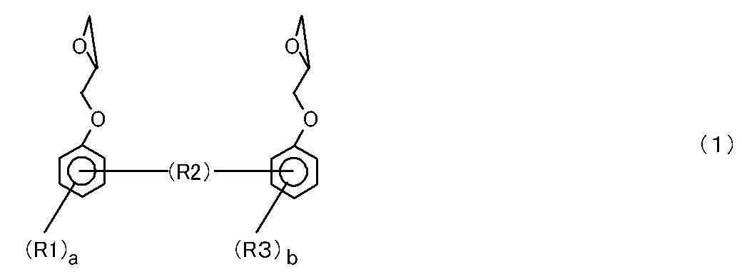
- the epoxy resin (A) is represented by the following general formula (1):
- R1 and R3 are hydrocarbon groups having 1 to 5 carbon atoms, and may be the same or different from each other.
- R2 is a direct bond and has 1 to 5 carbon atoms.
- -S- and -O-, a and b are integers of 0 to 4, which may be the same or different.
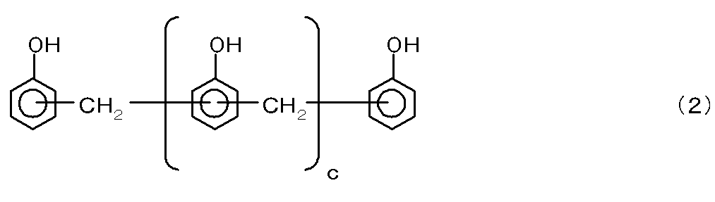
- the curing agent (B) is represented by the following general formula (2): (However, in the above general formula (2), c is an integer of 0 to 20.)
- the content of c 1 component contained in the total amount of the phenol resin (B1) represented by the general formula (2) as measured by the area method of the gel permeation chromatograph, including the phenol resin (B1) represented by The ratio is 40% or more in area fraction, and the content ratio of c ⁇ 4 components is 20% or less in area fraction. It is characterized by that.
- the phenol resin (B1) is a total amount of the phenol resin (B1) represented by the general formula (2) as measured by an area method of gel permeation chromatography.
- the epoxy resin (A1) is selected from the group consisting of alkyl group-substituted or unsubstituted biphenol, bisphenol A, bisphenol F, bisphenol S, bisphenol A / D, and oxybisphenol.
- the resulting phenol compound can be a crystalline epoxy resin obtained by diglycidyl etherification.
- the melting point is T A1
- the softening point of the phenol resin (B1) is T B1.
- can be 35 ° C. or less.
- the resin composition for encapsulating a semiconductor of the present invention can be used for encapsulating a semiconductor element by a transfer molding method using the resin composition for encapsulating a semiconductor as a tablet.
- the semiconductor device of the present invention is obtained by sealing a semiconductor element with a cured product of the above-described resin composition for encapsulating a semiconductor.
- This invention is a resin composition for semiconductor sealing containing an epoxy resin (A), a hardening
- the said epoxy resin (A) is represented by General formula (1).
- the epoxy resin (A1) having the structure as described above, the curing agent (B) contains the phenol resin (B1) represented by the general formula (2), and is measured by an area method of a gel permeation chromatograph,
- a semiconductor sealing resin composition having an excellent balance between tablet moldability and package moldability can be obtained.
- the present invention will be described in detail.
- an epoxy resin (A1) having a structure represented by the following general formula (1) is used as the epoxy resin (A).
- the substituents R1 and R3 are hydrocarbon groups having 1 to 5 carbon atoms, which may be the same or different from each other, and R2 is a direct bond and is a carbon atom having 1 to 5 carbon atoms.
- a hydrogen group, —S—, or —O—, and a and b are integers of 0 to 4, which may be the same or different.
- the epoxy resin (A1) having a structure represented by the general formula (1) has a low molecular weight, it has a low melt viscosity and can exhibit good fluidity.
- epoxy resins include diglycidyl ether compounds such as alkyl group-substituted or unsubstituted biphenol, bisphenol A, bisphenol F, bisphenol S, bisphenol A / D, and oxybisphenol.
- YSLV-80XY tetramethylbisphenol F type epoxy
- Nippon Steel Chemical Co., Ltd. YSLV-120TE (alkyl group-substituted bisphenol S type epoxy resin represented by the following formula (3))
- Japan Epoxy Resin Examples thereof include YX4000H (epoxy resin of tetramethylbiphenol), YL6810 (bisphenol A type epoxy resin) manufactured by Japan Epoxy Resin.
- R1 and R3 are hydrocarbon groups having 1 to 5 carbon atoms, and may be the same or different from each other.
- R2 is a direct bond and has 1 to 5 carbon atoms.
- -S- and -O-, a and b are integers of 0 to 4, which may be the same or different.
- the epoxy resin (A1) having the structure represented by the general formula (1) is not particularly limited as long as it has the above structure, but has a melting point, and the melting point is 40 ° C. or higher. Preferably, it is 45 degreeC or more.
- the lower limit of the melting point is within the above range, blocking is difficult to occur during transportation and storage of the epoxy resin raw material, and workability is less likely to be impaired.
- the upper limit of the melting point is not particularly limited, but is preferably 140 ° C. or lower, and more preferably 125 ° C. or lower. When the upper limit of the melting point is within the above range, there is little possibility of causing problems such as poor curability due to insufficient melting of the resin during melt kneading.
- Epoxy resins that can be used in combination include: novolak-type epoxy resins such as phenol novolac-type epoxy resins and cresol novolak-type epoxy resins; polyfunctional epoxy resins such as triphenolmethane-type epoxy resins and alkyl-modified triphenolmethane-type epoxy resins; Phenol aralkyl type epoxy resin, naphthol aralkyl type epoxy resin, phenol aralkyl type epoxy resin having biphenylene skeleton, aralkyl type epoxy resin such as naphthol aralkyl type epoxy resin having phenylene skeleton; dihydroxynaphthalene type epoxy resin, naphthol or dihydroxynaphthalene Naphthol-type epoxy resins such as epoxy resins obtained by glycidy
- the ionic impurities Na + ions and Cl ⁇ ions are as small as possible.
- the epoxy equivalent is 100 g / eq or more and 500 g. / Eq or less is preferable.
- the blending ratio of the epoxy resin (A1) having the structure represented by the general formula (1) when other epoxy resins are used in combination is 25% by mass or more based on the total epoxy resin (A). Preferably, it is more preferably 45% by mass or more, and particularly preferably 60% by mass or more.
- liquidity can be acquired as a compounding ratio is in the said range.
- the lower limit of the compounding ratio of the whole epoxy resin (A) It is preferable that it is 2 mass% or more in the resin composition for whole semiconductor sealing, and it is more preferable that it is 4 mass% or more. preferable.
- the lower limit of the blending ratio is within the above range, there is little possibility of causing a decrease in fluidity.
- the upper limit of the compounding ratio of the whole epoxy resin (A) It is preferable that it is 15 mass% or less in the resin composition for whole semiconductor sealing, and it is 13 mass% or less. Is more preferable.
- the upper limit of the blending ratio is within the above range, there is little possibility of causing a decrease in solder resistance.
- the resin composition for encapsulating a semiconductor of the present invention contains a phenol resin (B1) represented by the following general formula (2) as a curing agent (B), and is measured by a gel permeation chromatograph area method.
- the total of the phenol resin represented by 1 type or several general formula (2) contained in the resin composition for sealing is meant.
- the synthesis yield of the phenol resin (B1) represented by the general formula (2) is less likely to increase the cost due to being too low.
- the upper limit of the content ratio of c ⁇ 4 components contained in the total amount of the phenol resin (B1) represented by the general formula (2) is not particularly limited, but is preferably 20% or less in terms of area fraction. 15% or less is more preferable.
- the upper limit value of the content ratio of c ⁇ 4 components is within the above range, there is little possibility of causing a decrease in fluidity.
- the content rate of each above-mentioned component can be calculated
- the lower limit value of the softening point of the phenol resin (B1) represented by the general formula (2) is preferably 50 ° C. or higher, and more preferably 60 ° C. or higher. When the lower limit value of the softening point is within the above range, blocking is difficult to occur during transportation and storage of the epoxy resin raw material, and there is little risk of impairing workability.
- the upper limit value of the softening point is not particularly limited, but is preferably 140 ° C. or lower, and more preferably 125 ° C. or lower. When the upper limit value of the softening point is within the above range, there is little possibility of causing problems such as poor curability due to insufficient melting of the resin during melt kneading.
- the gel permeation chromatography (GPC) measurement of the phenol resin (B1) represented by the general formula (2) is performed to determine the PS equivalent molecular weight of each component corresponding to the detected peak, and the detected peak area The content ratio (area fraction) of each component corresponding to the peak detected from the ratio can be calculated.
- the gel permeation chromatography (GPC) measurement in the present invention is performed as follows.
- the GPC device is composed of a pump, an injector, a guard column, a column, and a detector, and tetrahydrofuran (THF) is used as a solvent.
- the pump flow rate is 0.5 ml / min. A flow rate higher than this is not preferable because the detection accuracy of the target molecular weight is lowered.
- the flow rate accuracy is preferably 0.10% or less.
- a commercially available guard column for example, TSK GUARDCOLUMN HHR-L: diameter 6.0 mm, tube length 40 mm
- a commercially available polystyrene gel column (TSK-GEL GMHHR- manufactured by Tosoh Corporation) are used for the guard column.
- L diameter 7.8 mm, tube length 30 mm
- a differential refractometer (RI detector, for example, a differential refractive index (RI) detector W2414 manufactured by WATERS) is used as the detector.
- RI detector for example, a differential refractive index (RI) detector W2414 manufactured by WATERS
- a calibration curve prepared from a monodisperse polystyrene (hereinafter referred to as PS) standard sample is used.
- PS monodisperse polystyrene
- a logarithmic value of the molecular weight of PS and the peak detection time (retention time) of PS are plotted, and a regression of the cubic equation is used.
- Standard PS samples for preparing a calibration curve include Shodex Standard SL-105 series product numbers S-1.0 (peak molecular weight 1060), S-1.3 (peak molecular weight 1310), S-2 manufactured by Showa Denko K.K. 0.0 (peak molecular weight 1990), S-3.0 (peak molecular weight 2970), S-4.5 (peak molecular weight 4490), S-5.0 (peak molecular weight 5030), S-6.9 (peak molecular weight 6930) ), S-11 (peak molecular weight 10700), S-20 (peak molecular weight 19900).
- the polymerization method and the component amount adjustment method can be used.
- the polymerization method include a method in which phenol and formaldehyde are polycondensed in the presence of an acid catalyst, and then a residual monomer and water are distilled off.
- a commercially available phenol novolak resin may be used.
- phenol having a predetermined molecular weight distribution, distillation, water washing, extraction, column chromatography fractionation described later, or A technique such as mixing novolac can be used.
- phenol a commercially available phenol monomer or a solution obtained by diluting phenol with a solvent can be used, but industrial phenol is preferable from the viewpoint of cost.
- formaldehyde a substance that is a formaldehyde generation source such as paraformaldehyde, trioxane, an aqueous formaldehyde solution, or a solution of these formaldehydes can be used. Usually, it is preferable to use an aqueous formaldehyde solution in terms of workability and cost.
- polymers obtained by polycondensation with phenol and aldehyde in advance under an acid catalyst distillates, extracts, molecular weight classification products, and bottoms may be used.
- commercially available bisphenol F or phenol novolac resin may be used in combination.
- the acid catalyst it is possible to use an acid catalyst that is generally known in the synthesis of phenol novolac resins.
- inorganic acids such as sulfuric acid, hydrochloric acid, phosphoric acid, phosphorous acid, or organic acids such as oxalic acid, formic acid, organic phosphonic acid, paratoluenesulfonic acid, dimethylsulfuric acid, zinc acetate, nickel acetate, etc. may be used. These can be used alone or in combination of two or more.
- oxalic acid and hydrochloric acid are preferable because the catalyst can be easily removed from the phenol resin.
- the reaction molar ratio (F / P molar ratio) of phenol (P) and formaldehyde (F) and the reaction temperature in the polycondensation of phenol and formaldehyde are not particularly limited, but the F / P molar ratio is usually 0.00.
- the reaction is preferably performed in the range of 05 to 0.7 mol and the reaction temperature in the range of 50 to 150 ° C.
- the average molecular weight can be reduced and the amount of c ⁇ 4 components can be adjusted low.
- the molecular weight adjustment method by distillation is not particularly limited, and examples thereof include atmospheric distillation, vacuum distillation, and steam distillation.
- the distillation operation is preferably performed at a temperature of 50 ° C. or higher and 250 ° C. or lower.
- the efficiency due to distillation deteriorates, which is not preferable from the viewpoint of productivity, and exceeds 250 ° C.
- the phenol novolac resin is decomposed and the molecular weight is increased, which is not preferable.
- water is distilled by atmospheric distillation at 100 to 150 ° C.
- the phenol monomer component is distilled by vacuum distillation at 150 to 200 ° C. and 5000 Pa.
- the molecular weight adjustment method by washing with water described above is carried out by adding water to a phenol novolac resin or a phenol novolac resin dissolved in an organic solvent at 20 to 150 ° C. under normal pressure or pressure. After stirring at room temperature, the aqueous phase and organic phase are separated by standing or centrifuging, and the aqueous phase is removed from the system, so that low molecular weight components dissolved in the aqueous phase, mainly phenol monomer components
- a nonpolar solvent having low solubility in a phenol resin such as toluene or xylene is dissolved in a phenol novolak resin, a phenol novolak resin aqueous solution, or a phenol resin dissolved in a polar solvent such as alcohol.
- the amount of c ⁇ 4 components can be reduced and adjusted.
- the molecular weight adjustment method using the separation column is as follows.
- a separation column filled with a separation funnel and polystyrene gel is connected in series with a refractive index (RI) detector and a separation collecting valve, and a phenol novolak is connected to the separation funnel.
- RI refractive index
- a phenol novolak is connected to the separation funnel.
- the refractive index (RI) chart is monitored, and the extraction solution from when a predetermined peak is detected until it disappears is collected. Any molecular weight component can be collected.
- the curing agent in the resin composition for semiconductor encapsulation of the present invention, other curing agents can be used in combination as long as the effect of using the phenol resin (B1) is not impaired.
- the curing agent that can be used in combination include a polyaddition type curing agent, a catalyst type curing agent, and a condensation type curing agent.
- the polyaddition type curing agent include aliphatic polyamines such as diethylenetriamine (DETA), triethylenetetramine (TETA), and metaxylenediamine (MXDA), diaminodiphenylmethane (DDM), m-phenylenediamine (MPDA), and diamino.
- aromatic polyamines such as diphenylsulfone (DDS), polyamine compounds including dicyandiamide (DICY), organic acid dihydralazide, and the like; alicyclic acid anhydrides such as hexahydrophthalic anhydride (HHPA) and methyltetrahydrophthalic anhydride (MTHPA) , Acid anhydrides including aromatic acid anhydrides such as trimellitic anhydride (TMA), pyromellitic anhydride (PMDA), benzophenone tetracarboxylic acid (BTDA); phenol aralkyl resins, dicyclopentadi Phenolic resin compound, such as down-modified phenolic resins; polysulfide, thioester, polymercaptan compounds such as thioethers; isocyanate prepolymer, isocyanate compounds such as blocked isocyanate; and organic acids such as carboxylic acid-containing polyester resins.
- DDS diphenylsulfone
- a phenol resin-based curing agent is preferable from the viewpoint of balance of flame resistance, moisture resistance, electrical properties, curability, storage stability, and the like.
- the phenolic resin-based curing agent is a monomer, oligomer, or polymer in general having two or more phenolic hydroxyl groups in one molecule, and its molecular weight and molecular structure are not particularly limited.
- novolak such as cresol novolac resin Type resin
- multifunctional phenol resin such as triphenolmethane type phenol resin
- modified phenol resin such as terpene modified phenol resin and dicyclopentadiene modified phenol resin
- phenol aralkyl resin having phenylene skeleton and / or biphenylene skeleton, phenylene and / or
- aralkyl type resins such as naphthol aralkyl resins having a biphenylene skeleton; bisphenol compounds such as bisphenol A and bisphenol AD, and the like
- the hydroxyl equivalent is preferably 90 g / eq or more and 250 g / eq or less from the viewpoint of curability.
- curing agent (B) It is preferable that it is 0.8 mass% or more in the resin composition for whole semiconductor sealing, and it is 1.5 mass% or more. It is more preferable. When the lower limit value of the blending ratio is within the above range, sufficient fluidity can be obtained. Further, the upper limit of the blending ratio of the entire curing agent (B) is not particularly limited, but is preferably 10% by mass or less, and 8% by mass or less in the resin composition for encapsulating all semiconductors. Is more preferable. When the upper limit of the blending ratio is within the above range, good solder resistance can be obtained.
- the equivalent ratio (EP) / (OH) to the number of phenolic hydroxyl groups (OH) of the entire resin-based curing agent is 0.8 or more and 1.3 or less.
- the equivalent ratio is within this range, sufficient curability can be obtained during molding of the resin composition for semiconductor encapsulation.
- the equivalent ratio is within this range, good physical properties in the resin cured product can be obtained.
- the epoxy resin (A1) has a melting point, the melting point is TA1, and the softening point of the phenol resin (B1) represented by the general formula (2) is
- T B1 is set, the absolute value
- the temperature difference between the melting point of the epoxy resin (A1) and the softening point of the phenol resin (B1) represented by the general formula (2) is within the above range, good tablet moldability can be obtained.
- curing agent it is preferable that it is 50 degreeC or more, and it is 60 degreeC or more. More preferred.
- the upper limit value of the softening point or melting point of the other epoxy resin and curing agent used in combination with the epoxy resin (A1) and the phenol resin (B1) is not particularly limited, but is preferably 140 ° C. or lower, and 125 ° C. The following is more preferable.
- the softening point or melting point of the other epoxy resin and curing agent used in combination with the epoxy resin (A1) and the phenol resin (B1) are within the above range, the appearance defect or defect of the tablet due to insufficient melting of the resin during melt kneading, etc. There is little risk of causing problems.
- an inorganic filler can be further used.
- the inorganic filler (C) that can be used in the resin composition for semiconductor encapsulation of the present invention those generally used in resin compositions for semiconductor encapsulation can be used, for example, fused silica, Examples thereof include spherical silica, crystalline silica, alumina, silicon nitride, and aluminum nitride.
- the particle size of the inorganic filler (C) is preferably 0.01 ⁇ m or more and 150 ⁇ m or less in consideration of the filling property into the mold cavity.
- an inorganic filler (C) As a lower limit of the content rate of an inorganic filler (C), it is preferable that it is 75 mass% or more of the whole resin composition for semiconductor sealing, it is more preferable that it is 80 mass% or more, and it is 83 mass% or more. It is particularly preferred.
- the lower limit value of the content ratio of the inorganic filler (C) is within the above range, the resin composition for semiconductor encapsulation can obtain good tablet moldability, and the cured product has increased moisture absorption. In addition, good solder crack resistance can be obtained without reducing the strength.
- an upper limit of the content rate of an inorganic filler (C) it is preferable that it is 93 mass% or less of the whole resin composition for semiconductor sealing, It is more preferable that it is 91 mass% or less, 90 mass% It is particularly preferred that When the upper limit value of the content ratio of the inorganic filler (C) is within the above range, the flowability is not impaired and good moldability can be obtained.
- a curing accelerator (D) can be further used.
- the curing accelerator (D) may be any one that accelerates the reaction between the epoxy group of the epoxy resin and the phenolic hydroxyl group of the compound containing two or more phenolic hydroxyl groups, and is used for a general semiconductor sealing resin composition. Can be used.
- phosphorus-containing compounds such as organic phosphines, tetra-substituted phosphonium compounds, phosphobetaine compounds, adducts of phosphine compounds and quinone compounds, adducts of phosphonium compounds and silane compounds; 1,8-diazabicyclo (5 , 4, 0) Undecene-7, benzyldimethylamine, 2-methylimidazole and the like nitrogen-containing compounds.
- phosphorus atom-containing compounds are preferred.
- tetra-substituted phosphonium compounds From the viewpoint of the balance between fluidity and curability, tetra-substituted phosphonium compounds, phosphobetaine compounds, adducts of phosphine compounds and quinone compounds, and additions of phosphonium compounds and silane compounds.
- a catalyst having latency such as a product is more preferable.
- a tetra-substituted phosphonium compound is particularly preferable, and in view of the low thermal modulus of the cured resin cured resin composition, an adduct of a phosphobetaine compound, a phosphine compound and a quinone compound is used.
- an adduct of a phosphonium compound and a silane compound is particularly preferable.
- Examples of the organic phosphine that can be used in the resin composition for encapsulating a semiconductor of the present invention include a first phosphine such as ethylphosphine and phenylphosphine; a second phosphine such as dimethylphosphine and diphenylphosphine; trimethylphosphine, triethylphosphine, and tributyl. Third phosphine such as phosphine and triphenylphosphine can be used.
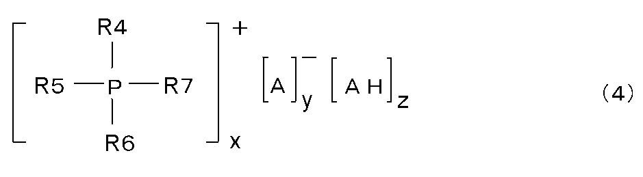
- Examples of the tetra-substituted phosphonium compound that can be used in the semiconductor sealing resin composition of the present invention include compounds represented by the following general formula (4).
- P represents a phosphorus atom.
- R4, R5, R6, and R7 represent an aromatic group or an alkyl group.
- A is a functional group chosen from a hydroxyl group, a carboxyl group, and a thiol group.
- X and y are integers of 1 to 3
- z is an integer of 0 to 3
- x y.
- the compound represented by the general formula (4) is obtained, for example, as follows, but is not limited thereto. First, a tetra-substituted phosphonium halide, an aromatic organic acid and a base are mixed in an organic solvent and mixed uniformly to generate an aromatic organic acid anion in the solution system. Then, when water is added, the compound represented by the general formula (4) can be precipitated.
- R4, R5, R6 and R7 bonded to the phosphorus atom are phenyl groups
- AH is a compound having a hydroxyl group in an aromatic ring, that is, phenols, and A Is preferably an anion of the phenol.
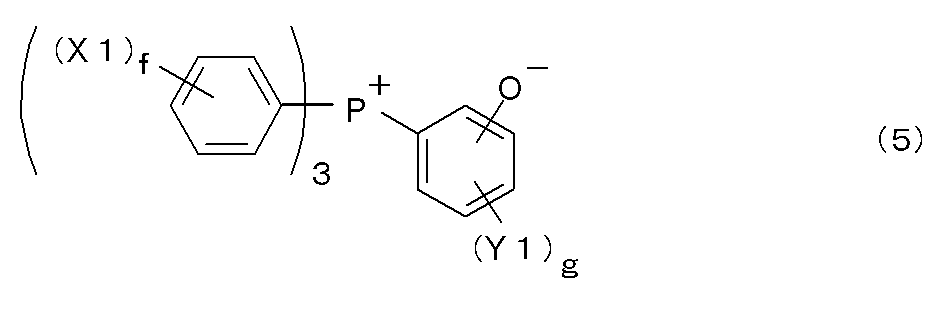
- Examples of the phosphobetaine compound that can be used in the semiconductor sealing resin composition of the present invention include compounds represented by the following general formula (5).
- X1 represents an alkyl group having 1 to 3 carbon atoms
- Y1 represents a hydroxyl group
- f is an integer of 0 to 5
- g is an integer of 0 to 4.
- the compound represented by the general formula (5) is obtained as follows, for example. First, it is obtained through a step of bringing a triaromatic substituted phosphine, which is a third phosphine, into contact with a diazonium salt and replacing the triaromatic substituted phosphine with a diazonium group of the diazonium salt.
- a triaromatic substituted phosphine which is a third phosphine
- the present invention is not limited to this.
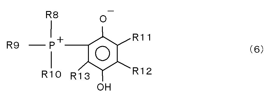
- Examples of the adduct of a phosphine compound and a quinone compound that can be used in the semiconductor sealing resin composition of the present invention include compounds represented by the following general formula (6).
- P represents a phosphorus atom.
- R8, R9 and R10 each represents an alkyl group having 1 to 12 carbon atoms or an aryl group having 6 to 12 carbon atoms, and may be the same as each other
- R11, R12 and R13 each represent a hydrogen atom or a hydrocarbon group having 1 to 12 carbon atoms, which may be the same or different from each other, and R11 and R12 are bonded to form a cyclic structure. May be.
- Examples of the phosphine compound used as an adduct of a phosphine compound and a quinone compound include an aromatic ring such as triphenylphosphine, tris (alkylphenyl) phosphine, tris (alkoxyphenyl) phosphine, trinaphthylphosphine, and tris (benzyl) phosphine.
- aromatic ring such as triphenylphosphine, tris (alkylphenyl) phosphine, tris (alkoxyphenyl) phosphine, trinaphthylphosphine, and tris (benzyl) phosphine.
- Those having a substituent or a substituent such as an alkyl group or an alkoxyl group are preferred.
- Examples of the substituent such as an alkyl group and an alkoxyl group include those having 1 to 6 carbon atoms. From the viewpoint of availability, tripheny
- examples of the quinone compound used for the adduct of the phosphine compound and the quinone compound include o-benzoquinone, p-benzoquinone and anthraquinones, and among them, p-benzoquinone is preferable from the viewpoint of storage stability.
- the adduct can be obtained by contacting and mixing in a solvent capable of dissolving both organic tertiary phosphine and benzoquinone.
- the solvent is preferably a ketone such as acetone or methyl ethyl ketone, which has low solubility in the adduct.
- the present invention is not limited to this.
- R8, R9 and R10 bonded to the phosphorus atom are phenyl groups, and R11, R12 and R13 are hydrogen atoms, that is, 1,4-benzoquinone and triphenyl
- R11, R12 and R13 are hydrogen atoms, that is, 1,4-benzoquinone and triphenyl
- a compound to which phosphine has been added is preferable in that it reduces the thermal elastic modulus of the cured product of the resin composition for semiconductor encapsulation.
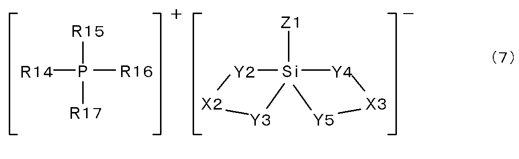
- Examples of the adduct of a phosphonium compound and a silane compound that can be used in the semiconductor sealing resin composition of the present invention include compounds represented by the following general formula (7).
- P represents a phosphorus atom and Si represents a silicon atom.
- R14, R15, R16 and R17 are each an organic group having an aromatic ring or a heterocyclic ring, or an aliphatic group.
- X2 is an organic group bonded to the groups Y2 and Y3, where X3 is an organic group bonded to the groups Y4 and Y5.
- Y3 represent a group formed by releasing a proton from a proton donating group, and groups Y2 and Y3 in the same molecule are bonded to a silicon atom to form a chelate structure, and Y4 and Y5 are proton donating groups.
- the group represents a group formed by releasing a proton, and the groups Y4 and Y5 in the same molecule are bonded to a silicon atom to form a chelate structure.
- X2 and X3 are the same or different from each other.
- Well, 2, Y3, Y4, and Y5 is .Z1 which may be the same or different from each other is an organic group or an aliphatic group, an aromatic ring or a heterocyclic ring.
- R14, R15, R16 and R17 for example, phenyl group, methylphenyl group, methoxyphenyl group, hydroxyphenyl group, naphthyl group, hydroxynaphthyl group, benzyl group, methyl group, ethyl group, n-butyl group, n-octyl group, cyclohexyl group, and the like.
- an aromatic group having a substituent such as phenyl group, methylphenyl group, methoxyphenyl group, hydroxyphenyl group, hydroxynaphthyl group, or the like.
- a substituted aromatic group is more preferred.
- X2 is an organic group bonded to Y2 and Y3.
- X3 is an organic group bonded to the groups Y4 and Y5.
- Y2 and Y3 are groups formed by proton-donating groups releasing protons, and groups Y2 and Y3 in the same molecule are combined with a silicon atom to form a chelate structure.
- Y4 and Y5 are groups formed by proton-donating groups releasing protons, and groups Y4 and Y5 in the same molecule are combined with a silicon atom to form a chelate structure.
- the groups X2 and X3 may be the same or different from each other, and the groups Y2, Y3, Y4, and Y5 may be the same or different from each other.
- the groups represented by -Y2-X2-Y3- and -Y4-X3-Y5- in general formula (7) are composed of groups obtained by releasing a proton from a proton donor. Examples of proton donors include catechol, pyrogallol, 1,2-dihydroxynaphthalene, 2,3-dihydroxynaphthalene, 2,2′-biphenol, 1,1′-bi-2-naphthol, and salicylic acid.
- 1-hydroxy-2-naphthoic acid 3-hydroxy-2-naphthoic acid, chloranilic acid, tannic acid, 2-hydroxybenzyl alcohol, 1,2-cyclohexanediol, 1,2-propanediol and glycerin.
- catechol 1,2-dihydroxynaphthalene, and 2,3-dihydroxynaphthalene are more preferable.
- Z1 in the general formula (7) represents an organic group or an aliphatic group having an aromatic ring or a heterocyclic ring, and specific examples thereof include a methyl group, an ethyl group, a propyl group, a butyl group, and a hexyl group.
- Reactions such as aliphatic hydrocarbon groups such as octyl group and aromatic hydrocarbon groups such as phenyl group, benzyl group, naphthyl group and biphenyl group, glycidyloxypropyl group, mercaptopropyl group, aminopropyl group and vinyl group Among them, a methyl group, an ethyl group, a phenyl group, a naphthyl group, and a biphenyl group are more preferable from the viewpoint of thermal stability.
- a silane compound such as phenyltrimethoxysilane and a proton donor such as 2,3-dihydroxynaphthalene are added to a flask containing methanol, and then dissolved.
- Sodium methoxide-methanol solution is added dropwise with stirring.
- crystals are precipitated. The precipitated crystals are filtered, washed with water, and vacuum dried to obtain an adduct of a phosphonium compound and a silane compound.
- the blending ratio of the curing accelerator (D) that can be used in the semiconductor sealing resin composition of the present invention is more preferably 0.1% by mass or more and 1% by mass or less in the total resin composition.
- the blending ratio of the curing accelerator (D) is within the above range, sufficient curability can be obtained.
- liquidity can be obtained as the mixture ratio of a hardening accelerator (D) exists in the said range.
- a compound (E) in which a hydroxyl group is bonded to each of two or more adjacent carbon atoms constituting an aromatic ring can be used.
- the compound (E) (hereinafter also referred to as “compound (E)”) in which a hydroxyl group is bonded to each of two or more adjacent carbon atoms constituting the aromatic ring is used as an epoxy resin (A).
- a phosphorus atom-containing curing accelerator having no latent property is used as a curing accelerator for promoting the crosslinking reaction with the curing agent (B), the reaction during the melt-kneading of the resin composition is suppressed. And a resin composition for semiconductor encapsulation can be obtained stably.
- the compound (E) also has an effect of lowering the melt viscosity of the resin composition for semiconductor encapsulation and improving the fluidity.
- a monocyclic compound represented by the following general formula (8) or a polycyclic compound represented by the following general formula (9) can be used. It may have a substituent.
- one of R18 and R22 is a hydroxyl group, and when one is a hydroxyl group, the other is a hydrogen atom, a hydroxyl group or a substituent other than a hydroxyl group.
- R19, R20 and R21 are hydrogen atoms
- one of R23 and R29 is a hydroxyl group, and when one is a hydroxyl group, the other is a hydrogen atom, a hydroxyl group or a substituent other than a hydroxyl group.
- R24, R25, R26, R27 is a hydrogen atom, a hydroxyl group or a substituent other than a hydroxyl group.
- the monocyclic compound represented by the general formula (8) include catechol, pyrogallol, gallic acid, gallic acid ester, and derivatives thereof.
- Specific examples of the polycyclic compound represented by the general formula (9) include 1,2-dihydroxynaphthalene, 2,3-dihydroxynaphthalene, and derivatives thereof.
- a compound in which a hydroxyl group is bonded to each of two adjacent carbon atoms constituting an aromatic ring is preferable because of easy control of fluidity and curability.
- the mother nucleus is a compound having a low volatility and a highly stable weighing naphthalene ring.
- the compound (E) can be a compound having a naphthalene ring such as 1,2-dihydroxynaphthalene, 2,3-dihydroxynaphthalene and derivatives thereof.
- These compounds (E) may be used individually by 1 type, or may use 2 or more types together.
- the compounding ratio of the compound (E) is preferably 0.01% by mass or more and 1% by mass or less, more preferably 0.03% by mass or more, 0.8% in the total semiconductor sealing resin composition. It is 0.05 mass% or less, Most preferably, it is 0.05 mass% or more and 0.5 mass% or less.
- the lower limit value of the compounding ratio of the compound (E) is within the above range, a sufficient viscosity reduction and fluidity improvement effect of the resin composition for semiconductor encapsulation can be obtained.
- an adhesion assistant (F) such as a silane coupling agent is further added in order to improve the adhesion between the epoxy resin (A) and the inorganic filler (C).
- adhesion assistant (F) such as a silane coupling agent
- examples thereof include, but are not limited to, epoxy silane, amino silane, ureido silane, mercapto silane, etc., which react between the epoxy resin and the inorganic filler to improve the interfacial strength between the epoxy resin and the inorganic filler. If it is.
- a silane coupling agent can also raise the effect of the compound (E) of reducing the melt viscosity of the resin composition for semiconductor sealing, and improving fluidity
- examples of the epoxy silane include ⁇ -glycidoxypropyltriethoxysilane, ⁇ -glycidoxypropyltrimethoxysilane, ⁇ -glycidoxypropylmethyldimethoxysilane, ⁇ - (3,4 epoxy) (Cyclohexyl) ethyltrimethoxysilane and the like.
- examples of aminosilane include ⁇ -aminopropyltriethoxysilane, ⁇ -aminopropyltrimethoxysilane, N- ⁇ (aminoethyl) ⁇ -aminopropyltrimethoxysilane, and N- ⁇ (aminoethyl) ⁇ -aminopropyl.
- Methyldimethoxysilane N-phenyl ⁇ -aminopropyltriethoxysilane, N-phenyl ⁇ -aminopropyltrimethoxysilane, N- ⁇ (aminoethyl) ⁇ -aminopropyltriethoxysilane, N-6- (aminohexyl) 3 -Aminopropyltrimethoxysilane, N-3- (trimethoxysilylpropyl) -1,3-benzenedimethanane and the like.
- ureidosilanes include ⁇ -ureidopropyltriethoxysilane and hexamethyldisilazane.
- mercaptosilane include ⁇ -mercaptopropyltrimethoxysilane.
- the blending ratio of the adhesion assistant (F) such as a silane coupling agent that can be used in the resin composition for semiconductor encapsulation of the present invention is 0.01% by mass or more and 1% by mass or less in the total resin composition. More preferably, it is 0.05 mass% or more and 0.8 mass% or less, Most preferably, it is 0.1 mass% or more and 0.6 mass% or less. If the blending ratio of the adhesion aid (F) such as a silane coupling agent is not less than the above lower limit value, the interface strength between the epoxy resin and the inorganic filler will not decrease, and good solder crack resistance in the semiconductor device Can be obtained.
- the blending ratio of the adhesion assistant (F) such as a silane coupling agent is within the above range, the water absorption of the cured product of the resin composition does not increase, and good solder crack resistance in a semiconductor device. Can be obtained.
- colorants such as carbon black, bengara and titanium oxide; natural waxes such as carnauba wax; synthetic waxes such as polyethylene wax; stearic acid and zinc stearate Release agents such as higher fatty acids and their metal salts or paraffin, etc .; low stress additives such as silicone oil and silicone rubber; inorganic ion exchangers such as bismuth oxide hydrate; metals such as aluminum hydroxide and magnesium hydroxide Additives such as hydroxides and flame retardants such as zinc borate, zinc molybdate, phosphazene, and antimony trioxide may be appropriately blended.
- the method for producing the resin composition for encapsulating a semiconductor of the present invention is not particular limitation on the method for producing the resin composition for encapsulating a semiconductor of the present invention, but a mixture of the above-described components and other additives, etc. in a predetermined amount is used at room temperature using, for example, a mixer, a jet mill, a ball mill or the like.
- a kneading machine such as a heating roll, a kneader or an extruder
- the resin composition is melted and kneaded while heating to about 90 to 120 ° C., and the kneaded resin composition is obtained.
- a granular or powdery resin composition can be obtained.
- the particle size of the resin composition powder or granule is preferably 5 mm or less. If it exceeds 5 mm, filling failure occurs at the time of tableting, and the variation in tablet weight increases.
- a tablet can be obtained by tableting the powder or granule of the obtained resin composition.
- a single-shot or multiple rotary tableting machine can be used as an apparatus used for tableting molding.
- the shape of the tablet is not particularly limited, but a columnar shape is preferable.
- the tableting pressure is preferably in the range of 400 ⁇ 10 4 to 3000 ⁇ 10 4 Pa. If the tableting pressure exceeds the above upper limit, the tablet may be broken immediately after tableting.
- the resin composition for semiconductor encapsulation may be molded and cured by a molding method such as transfer molding, compression molding, or injection molding.
- the semiconductor element sealed with the semiconductor device of the present invention is not particularly limited, and examples thereof include an integrated circuit, a large-scale integrated circuit, a transistor, a thyristor, a diode, and a solid-state imaging element.
- the form of the semiconductor device of the present invention is not particularly limited.
- the dual in-line package DIP
- the plastic lead chip carrier PLCC
- the quad flat package QFP
- the low profile package and the like.
- Quad Flat Package LQFP
- Small Outline Package SOP
- Small Outline J Lead Package SOJ
- Thin Small Outline Package TQFP
- Examples include a tape carrier package (TCP), a ball grid array (BGA), and a chip size package (CSP).
- the semiconductor device of the present invention in which a semiconductor element is encapsulated with a cured product of a resin composition for encapsulating a semiconductor by a molding method such as transfer molding is used as it is or at a temperature of about 80 ° C. to 200 ° C. for about 10 minutes to 10 hours. After being fully cured over time, it is mounted on an electronic device or the like.
- FIG. 1 is a view showing a cross-sectional structure of an example of a semiconductor device using a resin composition for encapsulating a semiconductor according to the present invention.
- the semiconductor element 1 is fixed on the die pad 3 via the die bond material cured body 2.
- the electrode pad of the semiconductor element 1 and the lead frame 5 are connected by a wire 4.
- the semiconductor element 1 is sealed with a cured body 6 of a semiconductor sealing resin composition.
- FIG. 2 is a view showing a cross-sectional structure of an example of a single-side sealed semiconductor device using the resin composition according to the present invention.
- the semiconductor element 1 is fixed on the substrate 8 via the solder resist 7 and the die bond material cured body 2.
- the electrode pads on the semiconductor element 1 and the electrode pads on the substrate 8 are connected by a wire 4 via a solder resist 7. Only the single side
- the electrode pads on the substrate 8 are bonded to the solder balls 9 on the non-sealing surface side on the substrate 8 inside.
- GPC gel permeation chromatography
- the GPC system includes WATERS module W2695, Tosoh Corporation TSK GUARDCOLUMN HHR-L (diameter 6.0 mm, tube length 40 mm, guard column), Tosoh Corporation TSK-GEL GMHHR-L (diameter 7.8 mm, A tube having a tube length of 30 mm and two polystyrene gel columns) and a differential refractive index (RI) detector W2414 manufactured by WATERS, in series, was used.
- the flow rate of the pump was 0.5 ml / min
- the temperature in the column and the differential refractometer was 40 ° C.
- measurement was performed by injecting the measurement solution from a 100 ⁇ l injector.
- a calibration curve prepared from a monodisperse polystyrene (hereinafter referred to as PS) standard sample is used.
- PS monodisperse polystyrene
- a logarithmic value of the molecular weight of PS and the peak detection time (retention time) of PS are plotted, and a regression of the cubic equation is used.
- Standard PS samples for preparing a calibration curve include Shodex Standard SL-105 series product numbers S-1.0 (peak molecular weight 1060), S-1.3 (peak molecular weight 1310), S-2 manufactured by Showa Denko K.K.
- Epoxy resin 1 Tetramethylbisphenol F type epoxy resin (manufactured by Toto Kasei Co., Ltd., YSLV-80XY. Epoxy equivalent 190, melting point 80 ° C.)
- Epoxy resin 2 bisphenol A type epoxy resin (manufactured by Japan Epoxy Resin Co., Ltd., YL6810. Epoxy equivalent 172, melting point 45 ° C.)
- Epoxy resin 3 Tetramethylbiphenyl type epoxy resin (manufactured by Japan Epoxy Resin Co., Ltd., YX4000H.
- Epoxy equivalent 185, melting point 107 ° C. Epoxy resin 4: Epoxy resin represented by the following formula (3) (manufactured by Toto Kasei Co., Ltd., YSLV-120TE. Epoxy equivalent 240, melting point 120 ° C.)
- Epoxy resin 5 Biphenylene skeleton-containing phenol aralkyl type epoxy resin (manufactured by Nippon Kayaku Co., Ltd., NC3000, epoxy equivalent 276, softening point 58 ° C.).
- Epoxy resin 6 dicyclopentadiene type epoxy resin (manufactured by Dainippon Ink and Chemicals, HP 7200L, epoxy equivalent 244, softening point 56 ° C.).
- Epoxy resin 7 Methoxynaphthalene type epoxy resin (Dainippon Ink & Chemicals, EXA7320, epoxy equivalent 251, softening point 58 ° C.).
- Epoxy resin 8 dihydroanthraquinone type epoxy resin (trade name YX8800 manufactured by Japan Epoxy Resin Co., Ltd., equivalent 180, melting point 110 ° C.)
- Curing agent 2 phenol novolak resin represented by the following general formula (2) (manufactured by Mitsui Chemicals, VR-9305.
- Curing agent 3 1700 parts by mass of phenol and 350 parts by mass of 37% formalin were charged into a reactor equipped with a stirrer, a thermometer and a cooler, and after adding 17 parts by mass of oxalic acid, the reaction temperature was 95 ° C. to 105 ° C. The reaction was continued for 4 hours.
- the temperature is raised to 180 ° C., distilled under reduced pressure at 5000 Pa to remove unreacted phenol, heated to 230 ° C., and steam distilled at a reduced pressure of 5000 Pa with a water vapor amount of 2 g / min.
- Curing agent 4 Phenol novolak resin represented by the following general formula (2) (manufactured by Sumitomo Bakelite Co., Ltd., PR-HF-3.
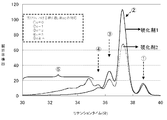
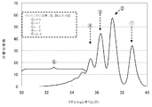
- Table 1 shows the content, number average molecular weight, and softening point of each component of curing agents 1 to 5 measured by gel permeation chromatography (GPC), and shows a gel permeation chromatography (GPC) chart of curing agents 1 and 2 It was shown in 3.
- the gel permeation chromatography (GPC) charts of the curing agents 3 to 5 are shown in FIGS. 4 to 6, respectively.
- Inorganic filler 1 100 parts by mass of fused spherical silica FB560 (average particle size 30 ⁇ m) manufactured by Denki Kagaku Kogyo, 6.5 parts by mass of synthetic spherical silica SO-C2 (average particle size 0.5 ⁇ m) manufactured by Admatex, synthesized by Admatex Pre-blended with 7.5 parts by mass of spherical silica SO-C5 (average particle size 30 ⁇ m).
- Curing accelerator 1 Curing accelerator represented by the following formula (10)
- Silane coupling agent 1 ⁇ -glycidoxypropyltrimethoxysilane (manufactured by Shin-Etsu Chemical Co., Ltd., KBM-403)
- Silane coupling agent 2 ⁇ -mercaptopropyltrimethoxysilane (manufactured by Shin-Etsu Chemical Co., Ltd., KBM-803)
- Silane coupling agent 3 N-phenyl-3-aminopropyltrimethoxysilane (manufactured by Shin-Etsu Chemical Co., Ltd., KBM-573)
- Colorant 1 Carbon black (Mitsubishi Chemical Industry Co., Ltd., MA600)
- Mold release agent 1 Carnauba wax (Nikko Fine Co., Ltd., Nikko Carnauba, melting point 83 ° C.)
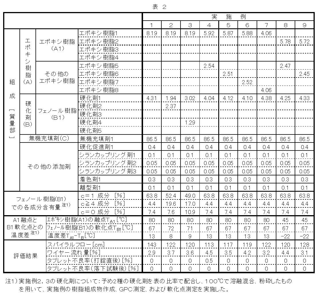
- Example 1 Epoxy resin 1 8.19 parts by mass Curing agent 1 4.31 parts by mass Inorganic filler 1 86.5 parts by mass Curing accelerator 1 0.4 parts by mass Silane coupling agent 1 0.1 parts by mass Silane coupling agent 2 0 0.05 part by weight Silane coupling agent 3 0.05 part by weight Colorant 1 0.3 part by weight Release agent 1 0.1 part by weight is mixed at room temperature with a mixer and melt-kneaded with a heating roll at 85 to 100 ° C. After being stretched into a sheet and cooled, it was pulverized with a hammer mill to obtain a powdery resin composition. The obtained resin composition was used and evaluated by the following method. The evaluation results are shown in Table 2.
- Tablet compression moldability The resin composition is adjusted using a powder molding press (S-20-A, manufactured by Tamagawa Machinery Co., Ltd.) so that the tablet weight is 15 g, size ⁇ 18 mm ⁇ height approximately 31 mm. 200 tablets were continuously tableted at a tableting pressure of 600 Pa. After tableting, the number of tablets with poor appearance and damage was counted and expressed in percent defective. Next, after packing 100 non-defective tablets into a cardboard box of interior polyethylene bags and dropping them 3 times from a height of 30 cm, the same appearance observation was performed and the defect rate (%) after the drop test was counted. did.
- S-20-A powder molding press manufactured by Tamagawa Machinery Co., Ltd.
- the flow rate of the most flowed (deformed) wire in one package is (F)
- the length of the wire is (L)
- the flow rate F / L ⁇ 100 (%) was calculated, and the average value of 10 packages is shown in Table 2.
- Examples 2 to 17, Comparative Examples 1 to 8 According to the composition of Table 2, Table 3, and Table 4, resin compositions were produced in the same manner as in Example 1, and evaluated in the same manner as in Example 1. The evaluation results are shown in Table 2, Table 3, and Table 4.
- two kinds of curing agents were blended in advance based on the ratios in Table 2, melted and mixed at 100 ° C., and further pulverized to prepare a mixer together with other raw materials. After mixing at room temperature, a powdery resin composition was obtained in the same manner as in Example 1.
- Examples 1 to 17 include an epoxy resin (A1) having a structure represented by the general formula (1), a phenol resin (B1) represented by the general formula (2), and a gel permeation chromatograph.
- the epoxy resin (A1) is changed in type and blending ratio
- c 1 component in the phenol resin (B1) represented by the general formula (2)
- the content ratio of ⁇ 4 components was changed, any of them resulted in an excellent balance of fluidity (spiral flow), wire flow, and tablet moldability.
- the area of the gel permeation chromatograph includes the epoxy resin (A1) having the structure represented by the general formula (1) and the phenol resin (B1) represented by the general formula (2).
Landscapes
- Chemical & Material Sciences (AREA)
- Health & Medical Sciences (AREA)
- Chemical Kinetics & Catalysis (AREA)
- Medicinal Chemistry (AREA)
- Polymers & Plastics (AREA)
- Organic Chemistry (AREA)
- Epoxy Resins (AREA)
- Structures Or Materials For Encapsulating Or Coating Semiconductor Devices Or Solid State Devices (AREA)
- Compositions Of Macromolecular Compounds (AREA)
Abstract
Description
前記エポキシ樹脂(A)が下記一般式(1):
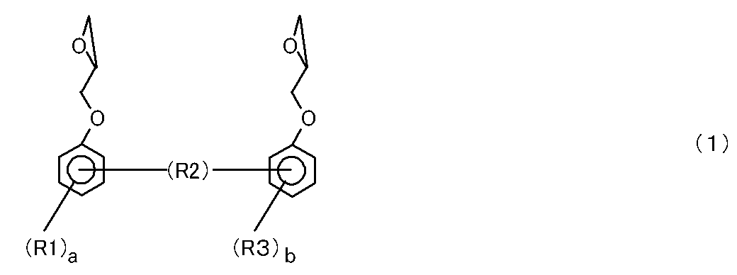
で表される構造を有するエポキシ樹脂(A1)を含み、
前記硬化剤(B)が下記一般式(2):

で表されるフェノール樹脂(B1)を含み、ゲルパーミエーションクロマトグラフの面積法による測定で、一般式(2)で表されるフェノール樹脂(B1)の全量中に含まれるc=1成分の含有割合が面積分率で40%以上であり、かつc≧4成分の含有割合が面積分率で20%以下である、
ことを特徴とする。


エポキシ樹脂1:テトラメチルビスフェノールF型エポキシ樹脂(東都化成(株)製、YSLV-80XY。エポキシ当量190、融点80℃。)
エポキシ樹脂2:ビスフェノールA型エポキシ樹脂(ジャパンエポキシレジン(株)製、YL6810。エポキシ当量172、融点45℃。)
エポキシ樹脂3:テトラメチルビフェニル型エポキシ樹脂(ジャパンエポキシレジン(株)製、YX4000H。エポキシ当量185、融点107℃。)
エポキシ樹脂4:下記式(3)で表されるエポキシ樹脂(東都化成(株)製、YSLV-120TE。エポキシ当量240、融点120℃。)
エポキシ樹脂5:ビフェニレン骨格含有フェノールアラルキル型エポキシ樹脂(日本化薬株式会社製、NC3000、エポキシ当量276、軟化点58℃)。
エポキシ樹脂6:ジシクロペンタジエン型エポキシ樹脂(大日本インキ化学工業株式会社製、HP7200L、エポキシ当量244、軟化点56℃)。
エポキシ樹脂7:メトキシナフタレン型エポキシ樹脂(大日本インキ化学工業株式会社製、EXA7320、エポキシ当量251、軟化点58℃)。
エポキシ樹脂8:ジヒドロアントラキノン型エポキシ樹脂(ジャパンエポキシレジン(株)製商品名YX8800、当量180、融点110℃)

硬化剤1:下記一般式(2)表されるフェノールノボラック樹脂(群栄化学(株)製、LV-70S。水酸基当量104、軟化点67℃、c=1成分の含有割合63.8%、c≧4成分の含有割合4.4%、c=0成分の含有割合7.4%、数平均分子量332)
硬化剤2:下記一般式(2)表されるフェノールノボラック樹脂(三井化学(株)製、VR-9305。水酸基当量104、軟化点75.5℃、c=1成分の含有割合43.1%、c≧4成分の含有割合32.1%、c=0成分の含有割合7.7%、数平均分子量391)
硬化剤3:撹拌機、温度計、冷却器を備えた反応器に、フェノール1700質量部、37%ホルマリン350質量部を仕込み、蓚酸17質量部を加えた後、反応温度を95℃~105℃に保ちながら4時間反応させた。その後、180℃まで昇温し、5000Paの減圧度で減圧蒸留を行って未反応のフェノールを除去した上で230℃まで昇温し、5000Paの減圧度で水蒸気量2g/minで水蒸気蒸留することによって、下記一般式(2)に表されるフェノールノボラック樹脂(水酸基当量104、軟化点64.4℃、c=1成分の含有割合33.1%、c≧4成分の含有割合11.7%、c=0成分の含有割合19.4%、数平均分子量338)を得た。
硬化剤4:下記一般式(2)表されるフェノールノボラック樹脂(住友ベークライト(株)製、PR-HF-3。水酸基当量104、軟化点80℃、c=1成分の含有割合14.5%、c≧4成分の含有割合46.5%、c=0成分の含有割合18.9%、数平均分子量437)
硬化剤5:硬化剤3の合成において、反応後の系中にビスフェノールF(試薬特級、4,4'-ジヒドロキシジフェニルメタン、和光純薬工業(株)製)80質量部を加え、水蒸気蒸留温度を230℃から215℃に変更した以外は、硬化剤3と同様の合成操作を行い、下記一般式(2)表されるフェノールノボラック樹脂(水酸基当量104、軟化点63.0℃、c=1成分の含有割合21.3%、c≧4成分の含有割合22.4%、c=0成分の含有割合32.1%、数平均分子量333)を得た。
ゲルパーミエーションクロマトグラフィー(GPC)で測定した硬化剤1~5の各成分含有量、数平均分子量、軟化点を表1に、硬化剤1及び2のゲルパーミエーションクロマトグラフィー(GPC)チャートを図3に示した。硬化剤3~5のゲルパーミエーションクロマトグラフィー(GPC)チャートをそれぞれ図4~6に示した。


無機充填剤1:電気化学工業製溶融球状シリカFB560(平均粒径30μm)100質量部、アドマテックス製合成球状シリカSO-C2(平均粒径0.5μm)6.5質量部、アドマテックス製合成球状シリカSO-C5(平均粒径30μm)7.5質量部とを予めブレンドしたもの。

シランカップリング剤1:γ-グリシドキシプロピルトリメトキシシラン(信越化学工業(株)製、KBM-403。)
シランカップリング剤2:γ-メルカプトプロピルトリメトキシシラン(信越化学工業(株)製、KBM-803。)
シランカップリング剤3:N-フェニル-3-アミノプロピルトリメトキシシラン(信越化学工業(株)製、KBM-573。)
着色剤1:カーボンブラック(三菱化学工業(株)製、MA600。)
離型剤1:カルナバワックス(日興ファイン(株)製、ニッコウカルナバ、融点83℃。)
エポキシ樹脂1 8.19質量部
硬化剤1 4.31質量部
無機充填剤1 86.5質量部
硬化促進剤1 0.4質量部
シランカップリング剤1 0.1質量部
シランカップリング剤2 0.05質量部
シランカップリング剤3 0.05質量部
着色剤1 0.3質量部
離型剤1 0.1質量部
をミキサーにて常温混合し、85~100℃の加熱ロールで溶融混練し、シート状に延伸させて冷却した後、ハンマーミルにより粉砕し、粉末状樹脂組成物を得た。得られた樹脂組成物を用いて以下の方法で評価した。評価結果を表2に示す。
表2、表3、表4の配合に従い、実施例1と同様にして樹脂組成物を製造し、実施例1と同様にして評価した。評価結果を表2、表3、表4に示す。なお、実施例2、3においては、予め2種の硬化剤を表2の比率に基づいて配合し、100℃で溶融混合し、さらに粉砕したものを作製したうえで、他の原料とともにミキサーにて常温混合し、その後は実施例1と同様にして粉末状樹脂組成物を得た。また、表2において記載した実施例2、3におけるフェノール樹脂(B1)の軟化点、およびc=1成分、c≧4成分、c=0成分の含有割合についても、予め2種の硬化剤を表2の比率に基づいて配合し、100℃で溶融混合し、さらに粉砕したものを作製して、軟化点の測定とゲルパーミエーションクロマトグラフィー(GPC)測定を行った。


この出願は、平成21年3月11日に出願された日本特許出願特願2009-057387を基礎とする優先権を主張し、その開示の全てをここに取り込む。
Claims (6)
- エポキシ樹脂(A)と硬化剤(B)と無機充填剤(C)とを含む半導体封止用樹脂組成物であって、
前記エポキシ樹脂(A)が下記一般式(1):

で表される構造を有するエポキシ樹脂(A1)を含み、
前記硬化剤(B)が下記一般式(2):

で表されるフェノール樹脂(B1)を含み、ゲルパーミエーションクロマトグラフの面積法による測定で、一般式(2)で表されるフェノール樹脂(B1)の全量中に含まれるc=1成分の含有割合が面積分率で40%以上であり、かつc≧4成分の含有割合が面積分率で20%以下である、
ことを特徴とする半導体封止用樹脂組成物。 - 前記フェノール樹脂(B1)が、ゲルパーミエーションクロマトグラフの面積法による測定で、前記一般式(2)で表されるフェノール樹脂(B1)の全量中に含まれるc=0成分の含有割合が面積分率で16%以下であることを特徴とする請求項1に記載の半導体封止用樹脂組成物。
- 前記エポキシ樹脂(A1)が、アルキル基置換又は非置換のビフェノール、ビスフェノールA、ビスフェノールF、ビスフェノールS、ビスフェノールA/D、オキシビスフェノールからなる群から選ばれたフェノール化合物をジグリシジルエーテル化した結晶性エポキシ樹脂であることを特徴とする請求項1又は請求項2に記載の半導体封止用樹脂組成物。
- 前記エポキシ樹脂(A1)が融点を持つものであり、その融点をTA1とし、前記フェノール樹脂(B1)の軟化点をTB1としたとき、両者の温度差の絶対値|TA1-TB1|が35℃以下であることを特徴とする請求項1ないし請求項3のいずれか1項に記載の半導体封止用樹脂組成物。
- 前記半導体封止用樹脂組成物が、タブレット状としてトランスファー成形法により半導体素子を封止するために用いられることを特徴とする請求項1ないし請求項4のいずれか1項に記載の半導体封止用樹脂組成物。
- 請求項1ないし請求項5のいずれか1項に記載の半導体封止用樹脂組成物の硬化物で半導体素子を封止して得られることを特徴とする半導体装置。
Priority Applications (4)
| Application Number | Priority Date | Filing Date | Title |
|---|---|---|---|
| SG2011064201A SG174269A1 (en) | 2009-03-11 | 2010-03-02 | Semiconductor-sealing resin composition and semiconductor device |
| JP2011503670A JP5578168B2 (ja) | 2009-03-11 | 2010-03-02 | 半導体封止用樹脂組成物及び半導体装置 |
| CN201080011187.5A CN102348736B (zh) | 2009-03-11 | 2010-03-02 | 半导体封装用树脂组合物和半导体装置 |
| US13/255,571 US8653205B2 (en) | 2009-03-11 | 2010-03-02 | Resin composition for encapsulating semiconductor and semiconductor device |
Applications Claiming Priority (2)
| Application Number | Priority Date | Filing Date | Title |
|---|---|---|---|
| JP2009057387 | 2009-03-11 | ||
| JP2009-057387 | 2009-03-11 |
Publications (1)
| Publication Number | Publication Date |
|---|---|
| WO2010103745A1 true WO2010103745A1 (ja) | 2010-09-16 |
Family
ID=42728043
Family Applications (1)
| Application Number | Title | Priority Date | Filing Date |
|---|---|---|---|
| PCT/JP2010/001410 Ceased WO2010103745A1 (ja) | 2009-03-11 | 2010-03-02 | 半導体封止用樹脂組成物及び半導体装置 |
Country Status (8)
| Country | Link |
|---|---|
| US (1) | US8653205B2 (ja) |
| JP (1) | JP5578168B2 (ja) |
| KR (1) | KR101640961B1 (ja) |
| CN (2) | CN102348736B (ja) |
| MY (1) | MY153000A (ja) |
| SG (1) | SG174269A1 (ja) |
| TW (1) | TWI473830B (ja) |
| WO (1) | WO2010103745A1 (ja) |
Cited By (5)
| Publication number | Priority date | Publication date | Assignee | Title |
|---|---|---|---|---|
| JP2012162583A (ja) * | 2011-02-03 | 2012-08-30 | Sumitomo Bakelite Co Ltd | 樹脂成形体及びその製造方法、ならびに、電子部品装置 |
| CN102786773A (zh) * | 2011-05-20 | 2012-11-21 | 日东电工株式会社 | 密封用薄片以及电子部件装置 |
| US20170121505A1 (en) * | 2011-05-13 | 2017-05-04 | Hitachi Chemical Company, Ltd. | Epoxy resin molding material for sealing and electronic component device |
| CN111936540A (zh) * | 2018-03-27 | 2020-11-13 | 明和化成株式会社 | 酚醛树脂及其制造方法、以及环氧树脂组合物及其固化物 |
| JP2024023329A (ja) * | 2015-11-03 | 2024-02-21 | エスダブリューアイエムシー・エルエルシー | ポリマーの作製に有用な液状エポキシ樹脂組成物 |
Families Citing this family (4)
| Publication number | Priority date | Publication date | Assignee | Title |
|---|---|---|---|---|
| US20120205822A1 (en) * | 2009-10-26 | 2012-08-16 | Yusuke Tanaka | Resin composition for encapsulating semiconductor and semiconductor device using the resin composition |
| CN108878377B (zh) * | 2018-06-28 | 2020-10-20 | 广东美的制冷设备有限公司 | 功率模块及其制作方法以及空调器 |
| KR102264929B1 (ko) * | 2018-12-20 | 2021-06-14 | 삼성에스디아이 주식회사 | 정제 상의 반도체 소자 밀봉용 에폭시 수지 조성물 및 이를 사용하여 밀봉된 반도체 장치 |
| TWI719419B (zh) * | 2019-03-11 | 2021-02-21 | 台光電子材料股份有限公司 | 環氧樹脂組成物及由其製成的物品 |
Citations (5)
| Publication number | Priority date | Publication date | Assignee | Title |
|---|---|---|---|---|
| JPH06239967A (ja) * | 1993-02-12 | 1994-08-30 | Toray Ind Inc | 半導体封止用エポキシ樹脂組成物 |
| JP2000191886A (ja) * | 1998-10-20 | 2000-07-11 | Nitto Denko Corp | 半導体封止用樹脂組成物およびそれを用いた半導体装置 |
| JP2000212390A (ja) * | 1999-01-19 | 2000-08-02 | Nitto Denko Corp | 半導体封止用エポキシ樹脂組成物およびそれを用いた半導体装置 |
| JP2002003578A (ja) * | 2000-06-21 | 2002-01-09 | Matsushita Electric Works Ltd | 封止用エポキシ樹脂組成物及び半導体装置 |
| JP2002037863A (ja) * | 2000-07-26 | 2002-02-06 | Matsushita Electric Works Ltd | 封止用エポキシ樹脂組成物及び半導体装置 |
Family Cites Families (14)
| Publication number | Priority date | Publication date | Assignee | Title |
|---|---|---|---|---|
| JPH0468019A (ja) * | 1990-07-06 | 1992-03-03 | Matsushita Electric Works Ltd | 液状樹脂封止材 |
| US5319005A (en) * | 1992-01-27 | 1994-06-07 | Hitachi Chemical Co., Ltd. | Epoxy resin molding material for sealing of electronic component |
| JPH06100665A (ja) * | 1992-09-18 | 1994-04-12 | Mitsui Toatsu Chem Inc | エポキシ樹脂組成物 |
| JPH0852734A (ja) | 1994-08-10 | 1996-02-27 | Sumitomo Bakelite Co Ltd | 半導体封止用タブレットの製造方法 |
| JP2551548B2 (ja) | 1994-11-16 | 1996-11-06 | 東芝ケミカル株式会社 | 半導体封止用成形材料のタブレット製造装置 |
| JPH10175210A (ja) | 1996-12-19 | 1998-06-30 | Sumitomo Bakelite Co Ltd | 半導体封止用エポキシ樹脂組成物のタブレットの製造方法 |
| JP2001316453A (ja) * | 2000-02-28 | 2001-11-13 | Sumitomo Bakelite Co Ltd | エポキシ樹脂組成物及び半導体装置 |
| WO2005056676A1 (ja) * | 2003-12-11 | 2005-06-23 | Hitachi Chemical Co., Ltd. | 封止用エポキシ樹脂成形材料および電子部品装置 |
| KR101081619B1 (ko) * | 2004-11-30 | 2011-11-09 | 스미토모 베이클라이트 가부시키가이샤 | 에폭시 수지 조성물 및 반도체장치 |
| WO2007125635A1 (ja) * | 2006-03-31 | 2007-11-08 | Sumitomo Bakelite Co., Ltd. | 半導体封止用樹脂組成物及び半導体装置 |
| JP5069441B2 (ja) * | 2006-09-26 | 2012-11-07 | パナソニック株式会社 | 片面封止型半導体装置製造用エポキシ樹脂組成物及び片面封止型半導体装置 |
| KR101090654B1 (ko) * | 2006-10-02 | 2011-12-07 | 히다치 가세고교 가부시끼가이샤 | 밀봉용 에폭시 수지 성형 재료 및 전자 부품 장치 |
| JP5554500B2 (ja) * | 2007-01-25 | 2014-07-23 | パナソニック株式会社 | プリプレグ、プリント配線板、多層回路基板、プリント配線板の製造方法 |
| JP5357576B2 (ja) * | 2009-02-27 | 2013-12-04 | パナソニック株式会社 | 半導体封止用エポキシ樹脂組成物、及び半導体装置 |
-
2010
- 2010-03-02 JP JP2011503670A patent/JP5578168B2/ja not_active Expired - Fee Related
- 2010-03-02 WO PCT/JP2010/001410 patent/WO2010103745A1/ja not_active Ceased
- 2010-03-02 US US13/255,571 patent/US8653205B2/en not_active Expired - Fee Related
- 2010-03-02 MY MYPI2011004032 patent/MY153000A/en unknown
- 2010-03-02 KR KR1020117023327A patent/KR101640961B1/ko not_active Expired - Fee Related
- 2010-03-02 SG SG2011064201A patent/SG174269A1/en unknown
- 2010-03-02 CN CN201080011187.5A patent/CN102348736B/zh not_active Expired - Fee Related
- 2010-03-02 CN CN201410181157.9A patent/CN103965584B/zh not_active Expired - Fee Related
- 2010-03-10 TW TW99106880A patent/TWI473830B/zh not_active IP Right Cessation
Patent Citations (5)
| Publication number | Priority date | Publication date | Assignee | Title |
|---|---|---|---|---|
| JPH06239967A (ja) * | 1993-02-12 | 1994-08-30 | Toray Ind Inc | 半導体封止用エポキシ樹脂組成物 |
| JP2000191886A (ja) * | 1998-10-20 | 2000-07-11 | Nitto Denko Corp | 半導体封止用樹脂組成物およびそれを用いた半導体装置 |
| JP2000212390A (ja) * | 1999-01-19 | 2000-08-02 | Nitto Denko Corp | 半導体封止用エポキシ樹脂組成物およびそれを用いた半導体装置 |
| JP2002003578A (ja) * | 2000-06-21 | 2002-01-09 | Matsushita Electric Works Ltd | 封止用エポキシ樹脂組成物及び半導体装置 |
| JP2002037863A (ja) * | 2000-07-26 | 2002-02-06 | Matsushita Electric Works Ltd | 封止用エポキシ樹脂組成物及び半導体装置 |
Cited By (12)
| Publication number | Priority date | Publication date | Assignee | Title |
|---|---|---|---|---|
| JP2012162583A (ja) * | 2011-02-03 | 2012-08-30 | Sumitomo Bakelite Co Ltd | 樹脂成形体及びその製造方法、ならびに、電子部品装置 |
| US20170121505A1 (en) * | 2011-05-13 | 2017-05-04 | Hitachi Chemical Company, Ltd. | Epoxy resin molding material for sealing and electronic component device |
| JP2017222881A (ja) * | 2011-05-13 | 2017-12-21 | 日立化成株式会社 | 封止用エポキシ樹脂成形材料及び電子部品装置 |
| CN109971122A (zh) * | 2011-05-13 | 2019-07-05 | 日立化成株式会社 | 密封用环氧树脂成形材料及电子部件装置 |
| US10662315B2 (en) * | 2011-05-13 | 2020-05-26 | Hitachi Chemical Company, Ltd. | Epoxy resin molding material for sealing and electronic component device |
| CN102786773A (zh) * | 2011-05-20 | 2012-11-21 | 日东电工株式会社 | 密封用薄片以及电子部件装置 |
| US20120296010A1 (en) * | 2011-05-20 | 2012-11-22 | Nitto Denko Corporation | Encapsulating sheet and electronic device |
| JP2024023329A (ja) * | 2015-11-03 | 2024-02-21 | エスダブリューアイエムシー・エルエルシー | ポリマーの作製に有用な液状エポキシ樹脂組成物 |
| US12351677B2 (en) | 2015-11-03 | 2025-07-08 | Swimc Llc | Liquid epoxy resin composition useful for making polymers |
| JP7787136B2 (ja) | 2015-11-03 | 2025-12-16 | エスダブリューアイエムシー・エルエルシー | ポリマーの作製に有用な液状エポキシ樹脂組成物 |
| CN111936540A (zh) * | 2018-03-27 | 2020-11-13 | 明和化成株式会社 | 酚醛树脂及其制造方法、以及环氧树脂组合物及其固化物 |
| CN111936540B (zh) * | 2018-03-27 | 2023-10-03 | Ube株式会社 | 酚醛树脂及其制造方法、以及环氧树脂组合物及其固化物 |
Also Published As
| Publication number | Publication date |
|---|---|
| JP5578168B2 (ja) | 2014-08-27 |
| TW201037005A (en) | 2010-10-16 |
| CN102348736B (zh) | 2014-08-13 |
| JPWO2010103745A1 (ja) | 2012-09-13 |
| MY153000A (en) | 2014-12-31 |
| CN103965584B (zh) | 2016-06-22 |
| US20120001350A1 (en) | 2012-01-05 |
| US8653205B2 (en) | 2014-02-18 |
| CN103965584A (zh) | 2014-08-06 |
| TWI473830B (zh) | 2015-02-21 |
| CN102348736A (zh) | 2012-02-08 |
| KR101640961B1 (ko) | 2016-07-19 |
| SG174269A1 (en) | 2011-10-28 |
| KR20110131263A (ko) | 2011-12-06 |
Similar Documents
| Publication | Publication Date | Title |
|---|---|---|
| JP5578168B2 (ja) | 半導体封止用樹脂組成物及び半導体装置 | |
| CN104114639B (zh) | 封装用树脂组合物和使用其的电子装置 | |
| JP5708486B2 (ja) | 半導体封止用樹脂組成物及び半導体装置 | |
| KR20120101413A (ko) | 반도체 봉지용 수지 조성물 및 이것을 이용한 반도체 장치 | |
| KR20120040183A (ko) | 반도체 밀봉용 수지 조성물, 및 반도체 장치 | |
| WO2007125635A1 (ja) | 半導体封止用樹脂組成物及び半導体装置 | |
| JP5292930B2 (ja) | 半導体封止用エポキシ樹脂組成物及び半導体装置 | |
| JP5494137B2 (ja) | 半導体封止用樹脂組成物および半導体装置 | |
| KR20180136494A (ko) | 에폭시 수지 조성물 및 전자 부품 장치 | |
| JP5386836B2 (ja) | 半導体封止用樹脂組成物及び半導体装置 | |
| JP5573343B2 (ja) | 半導体封止用樹脂組成物、および半導体装置 | |
| JP5126045B2 (ja) | 半導体封止用樹脂組成物及び半導体装置 | |
| JP5050923B2 (ja) | 半導体封止用エポキシ樹脂組成物及び半導体装置 | |
| JP5651968B2 (ja) | 半導体封止用樹脂組成物及び半導体装置 | |
| JP5565081B2 (ja) | 半導体封止用樹脂組成物、および半導体装置 | |
| JP5316282B2 (ja) | 半導体封止用エポキシ樹脂組成物及び半導体装置 | |
| JP5868573B2 (ja) | 半導体封止用樹脂組成物及び半導体装置 | |
| JP5673237B2 (ja) | 封止用樹脂組成物及び電子部品装置 | |
| JP5211737B2 (ja) | 半導体封止用エポキシ樹脂組成物及び半導体装置 | |
| JP5488394B2 (ja) | 半導体封止用樹脂組成物及び半導体装置 | |
| JP5488393B2 (ja) | 半導体封止用樹脂組成物及び半導体装置 |
Legal Events
| Date | Code | Title | Description |
|---|---|---|---|
| WWE | Wipo information: entry into national phase |
Ref document number: 201080011187.5 Country of ref document: CN |
|
| 121 | Ep: the epo has been informed by wipo that ep was designated in this application |
Ref document number: 10750504 Country of ref document: EP Kind code of ref document: A1 |
|
| WWE | Wipo information: entry into national phase |
Ref document number: 2011503670 Country of ref document: JP |
|
| WWE | Wipo information: entry into national phase |
Ref document number: 13255571 Country of ref document: US |
|
| NENP | Non-entry into the national phase |
Ref country code: DE |
|
| ENP | Entry into the national phase |
Ref document number: 20117023327 Country of ref document: KR Kind code of ref document: A |
|
| 122 | Ep: pct application non-entry in european phase |
Ref document number: 10750504 Country of ref document: EP Kind code of ref document: A1 |