WO2010095608A1 - 硫化物及び光電素子 - Google Patents
硫化物及び光電素子 Download PDFInfo
- Publication number
- WO2010095608A1 WO2010095608A1 PCT/JP2010/052242 JP2010052242W WO2010095608A1 WO 2010095608 A1 WO2010095608 A1 WO 2010095608A1 JP 2010052242 W JP2010052242 W JP 2010052242W WO 2010095608 A1 WO2010095608 A1 WO 2010095608A1
- Authority
- WO
- WIPO (PCT)
- Prior art keywords
- sulfide
- ratio
- layer
- substrate
- light
- Prior art date
- Legal status (The legal status is an assumption and is not a legal conclusion. Google has not performed a legal analysis and makes no representation as to the accuracy of the status listed.)
- Ceased
Links
Images

Classifications
-
- H—ELECTRICITY
- H01—ELECTRIC ELEMENTS
- H01M—PROCESSES OR MEANS, e.g. BATTERIES, FOR THE DIRECT CONVERSION OF CHEMICAL ENERGY INTO ELECTRICAL ENERGY
- H01M14/00—Electrochemical current or voltage generators not provided for in groups H01M6/00 - H01M12/00; Manufacture thereof
- H01M14/005—Photoelectrochemical storage cells
-
- C—CHEMISTRY; METALLURGY
- C01—INORGANIC CHEMISTRY
- C01G—COMPOUNDS CONTAINING METALS NOT COVERED BY SUBCLASSES C01D OR C01F
- C01G19/00—Compounds of tin
- C01G19/006—Compounds containing tin, with or without oxygen or hydrogen, and containing two or more other elements
-
- H—ELECTRICITY
- H01—ELECTRIC ELEMENTS
- H01G—CAPACITORS; CAPACITORS, RECTIFIERS, DETECTORS, SWITCHING DEVICES, LIGHT-SENSITIVE OR TEMPERATURE-SENSITIVE DEVICES OF THE ELECTROLYTIC TYPE
- H01G9/00—Electrolytic capacitors, rectifiers, detectors, switching devices, light-sensitive or temperature-sensitive devices; Processes of their manufacture
- H01G9/20—Light-sensitive devices
- H01G9/2027—Light-sensitive devices comprising an oxide semiconductor electrode
- H01G9/2031—Light-sensitive devices comprising an oxide semiconductor electrode comprising titanium oxide, e.g. TiO2
-
- H—ELECTRICITY
- H10—SEMICONDUCTOR DEVICES; ELECTRIC SOLID-STATE DEVICES NOT OTHERWISE PROVIDED FOR
- H10F—INORGANIC SEMICONDUCTOR DEVICES SENSITIVE TO INFRARED RADIATION, LIGHT, ELECTROMAGNETIC RADIATION OF SHORTER WAVELENGTH OR CORPUSCULAR RADIATION
- H10F77/00—Constructional details of devices covered by this subclass
- H10F77/10—Semiconductor bodies
- H10F77/12—Active materials
-
- C—CHEMISTRY; METALLURGY
- C01—INORGANIC CHEMISTRY
- C01P—INDEXING SCHEME RELATING TO STRUCTURAL AND PHYSICAL ASPECTS OF SOLID INORGANIC COMPOUNDS
- C01P2002/00—Crystal-structural characteristics
- C01P2002/50—Solid solutions
- C01P2002/52—Solid solutions containing elements as dopants
- C01P2002/54—Solid solutions containing elements as dopants one element only
-
- Y—GENERAL TAGGING OF NEW TECHNOLOGICAL DEVELOPMENTS; GENERAL TAGGING OF CROSS-SECTIONAL TECHNOLOGIES SPANNING OVER SEVERAL SECTIONS OF THE IPC; TECHNICAL SUBJECTS COVERED BY FORMER USPC CROSS-REFERENCE ART COLLECTIONS [XRACs] AND DIGESTS
- Y02—TECHNOLOGIES OR APPLICATIONS FOR MITIGATION OR ADAPTATION AGAINST CLIMATE CHANGE
- Y02E—REDUCTION OF GREENHOUSE GAS [GHG] EMISSIONS, RELATED TO ENERGY GENERATION, TRANSMISSION OR DISTRIBUTION
- Y02E10/00—Energy generation through renewable energy sources
- Y02E10/50—Photovoltaic [PV] energy
- Y02E10/542—Dye sensitized solar cells
Definitions
- the present invention relates to a sulfide and a photoelectric element, and more specifically, a sulfide suitable as a material for a photoelectric element such as a thin film solar cell, a photoconductive cell, a photodiode, a phototransistor, a sensitized solar cell, and the like.
- a photoelectric element such as a thin film solar cell, a photoconductive cell, a photodiode, a phototransistor, a sensitized solar cell, and the like.
- the present invention relates to a photoelectric element.
- Photoelectric element refers to an element that can convert photon energy into an electrical signal (photoelectric conversion) through some physical phenomenon.
- a solar cell is a kind of photoelectric element, and can efficiently convert light energy of sunlight into electrical energy.
- the semiconductor used in solar cells monocrystalline Si, polycrystalline Si, amorphous Si, GaAs, InP, CdTe, CuIn 1-x Ga x Se 2 (CIGS), Cu 2 ZnSnS 4 (CZTS) such as is known Yes.
- CIGS chalcogenite-based compounds represented by CIGS and CZTS have a large light absorption coefficient, so that a thin film advantageous for cost reduction is possible.
- solar cells using CIGS as the light absorption layer have the highest conversion efficiency among thin-film solar cells, and conversion efficiency exceeding that of solar cells using polycrystalline Si is also obtained.
- CIGS has a problem that it contains an environmental load element and a rare element.
- CZTS has a band gap energy (1.4 to 1.5 eV) suitable for solar cells, and is characterized by being free from environmentally hazardous elements and rare elements.
- a solar cell using CZTS as a light absorption layer has a problem that conversion efficiency is lower than a solar cell using a conventional semiconductor as a light absorption layer.
- Non-Patent Document 1 A soda-lime glass (SLG) substrate coated with Mo is placed in a vacuum vessel, and a precursor film is formed on the substrate by co-sputtering using ZnS, SnS, and Cu as targets, (2) A method of manufacturing a CZTS type solar cell is disclosed in which the substrate is transferred to an annealing vessel, N 2 + H 2 S (20%) reaction gas is introduced into the annealing vessel, and annealing is performed at 580 ° C. for 3 hours. .
- Non-Patent Document 2 includes (1) A Cu / Sn / ZnS stack precursor or a Sn / Cu / ZnS stack precursor is formed on a Mo-coated SLG substrate using an electron beam evaporation method, (2) A method for producing CZTS in which a precursor is sulfided in a 5% H 2 S + N 2 atmosphere is disclosed.
- the characteristics required for a light absorption layer used for a photoelectric element such as a solar cell are not only high conversion efficiency but also an open-circuit voltage V OC , a short-circuit current density I SC , a form factor (fill factor) F.F. Etc. are also required to be expensive.
- V OC open-circuit voltage
- I SC short-circuit current density
- F.F. Etc. form factor
- the problem to be solved by the present invention is to provide a sulfide having a relatively high plurality of characteristics such as conversion efficiency, open-circuit voltage, short-circuit current density, form factor, etc., and a photoelectric element using the same. It is to provide.
- the sulfide according to the present invention is summarized as having the following configuration.
- the sulfide contains Cu, Zn, and Sn as main components.
- the composition (x, y) of the sulfide is A (0.78, 1.32), B (0.86, 1.32), C (0.86, 1.28), D (0.90).
- the gist of the photoelectric device according to the present invention is the use of the sulfide according to the present invention.
- a sulfide mainly composed of Cu, Zn and Sn conversion efficiency is improved by optimizing the atomic ratio of Cu, Zn and Sn so that the Cu / (Zn + Sn) ratio and the Zn / Sn ratio are within a certain range.
- a sulfide having a high open-circuit voltage V OC , a short-circuit current density I SC , and a form factor FF can be obtained.
- a photoelectric device having not only high characteristics but also an excellent balance of characteristics can be obtained.
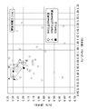
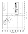
- Cu / (Zn + Sn) ratio CZTS-(x value) and Zn / Sn ratio (y value) is a diagram showing the relationship between conversion efficiency CZTS (E ff). It is a figure which shows the relationship between Cu / (Zn + Sn) ratio (x value) and Zn / Sn ratio (y value) of CZTS, and the open end voltage ( VOC ) of CZTS.
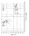
- Cu / (Zn + Sn) ratio CZTS-(x value) and Zn / Sn ratio (y value) is a diagram showing the relationship between the short-circuit current density CZTS (I SC). It is a figure which shows the relationship between the Cu / (Zn + Sn) ratio (x value) and Zn / Sn ratio (y value) of CZTS, and the shape factor (FF) of CZTS.
- the gist of the sulfide according to the present invention is as follows. (1) The sulfide contains Cu, Zn, and Sn as main components. (2) In the case where the Cu / (Zn + Sn) ratio and the Zn / Sn ratio (both atomic ratios) are x and y, respectively, and the composition is represented by coordinates of (x, y), The composition (x, y) of sulfide is A (0.78, 1.32), B (0.86, 1.32), C (0.86, 1.28), D (0.90, 1.23), E (0.90, 1.18), F (0.78, 1.28) of each straight line connecting A ⁇ B ⁇ C ⁇ D ⁇ E ⁇ F ⁇ A Above or inside the area enclosed by each of these straight lines.
- Sulfide containing Cu, Zn, and Sn as main components refers to a Cu 2 ZnSnS 4 (CZTS) -based compound.
- CZTS is a semiconductor having a band gap of about 1.45 eV and a light absorption coefficient of 10 4 cm ⁇ 1 or more.
- CZTS has low power generation efficiency in the stoichiometric composition, but shows relatively high conversion efficiency when Cu is slightly reduced compared to the stoichiometric composition.
- the term “sulfide containing Cu, Zn, and Sn as main components” refers not only to a compound having a stoichiometric composition, but also to all non-stoichiometric compounds showing relatively high conversion efficiency, or Cu , Zn, Sn, and all compounds containing S as the main component are included.
- the sulfide may be composed only of Cu, Zn, Sn and S, or may further contain various dopants and inevitable impurities in addition to these.
- composition (x, y) of the sulfide according to the present invention is: A (0.78, 1.32), B (0.86, 1.32), C (0.86, 1.28), D (0.90, 1.23), E (0.90, 1.18), F (0.78, 1.28) Are located on the straight lines connecting the points in the order of A ⁇ B ⁇ C ⁇ D ⁇ E ⁇ F ⁇ A or inside the area surrounded by these straight lines.
- any one or more of conversion efficiency, open-circuit voltage V OC , short-circuit current density I SC , and form factor FF will be reduced. The balance gets worse.
- the sulfide according to the present invention includes: (1) After a Cu—Zn—Sn or Cu—Zn—Sn—S precursor film is formed on the substrate surface by sputtering or the like, the precursor film is heat-treated in a hydrogen sulfide atmosphere or a vaporized sulfur atmosphere. how to, (2) A solution in which an organic metal or the like is dissolved is coated on a substrate and dried in air to cause hydrolysis and degeneracy reaction to form a metal oxide thin film containing Cu, Zn and Sn.
- Sol-gel + sulfurization method in which thin film is heat-treated in hydrogen sulfide atmosphere or vaporized sulfur atmosphere, (3) A method of forming a thin film made of the sulfide according to the present invention on the substrate surface by various methods, and scraping the thin film from the substrate to obtain a powder; (4) A method of mixing two or more sulfides containing one or more of Cu, Zn, or Sn, and subjecting the mixture to a solid phase reaction, (5) Two or more metal powders containing at least one of Cu, Zn, and Sn are mixed at a predetermined ratio, and the mixed powder is sulfurized with a sulfur source (for example, hydrogen sulfide, vaporized sulfur, sulfur powder, etc.).
- a sulfur source for example, hydrogen sulfide, vaporized sulfur, sulfur powder, etc.
- Heat treatment method in, (9) A solution in which a metal salt or metal sulfide is dissolved is sprayed in a high temperature atmosphere to form a Cu—Zn—Sn—S precursor, and then the precursor film is placed in a hydrogen sulfide atmosphere or a vaporized sulfur atmosphere.
- Heat treatment method (10) A method of forming a metal or metal sulfide raw material containing Cu, Zn, and Sn on a heated substrate by sputtering or the like, (11) A method of forming a metal or metal sulfide raw material containing Cu, Zn, and Sn, in addition to the S raw material on a heated substrate by sputtering or the like, (12) A method of performing a heat treatment in a hydrogen sulfide atmosphere or a vaporized sulfur atmosphere after forming a metal or metal sulfide raw material containing Cu, Zn, and Sn on a heated substrate by sputtering or the like, (13) A metal or metal sulfide raw material containing Cu, Zn, and Sn, and in addition, after forming the S raw material on a heated substrate by sputtering or the like, in a hydrogen sulfide atmosphere or a vaporized sulfur atmosphere Heat treatment method, Etc. can be manufactured.
- the sulfide is produced in the presence of Na.
- the conversion efficiency of sulfide is improved. This is considered because Na promotes the grain growth of sulfide.
- “producing sulfide in the presence of Na” means that Na is present around the sulfide or its precursor in the process of sulfide synthesis or grain growth.
- a material containing Na for example, SLG
- Na in the substrate is diffused to the thin film during heat treatment for producing sulfide.
- a Na-containing compound for example, Na 2 S
- the sulfide when the sulfide is produced in the presence of Na, it is preferable to wash the sulfide with a polar solvent after the sulfide is produced.
- a polar solvent When sulfides are synthesized in the presence of Na, crystal grains grow with Na, but Na itself is hardly dissolved in sulfides. Therefore, Na remains on the surface or inside of the sulfide after completion of the synthesis reaction. The remaining Na is considered to be combined with oxygen in the atmosphere to form Na—O-based particles. Since Na—O-based particles are insulators, they cause a reduction in sulfide conversion efficiency. Washing with a polar solvent is performed to remove the Na—O-based particles.
- a polar solvent capable of dissolving Na—O-based particles specifically, (1) water, (2) Inorganic acids such as hydrochloric acid, nitric acid, sulfuric acid or aqueous solutions thereof, (3) organic acids such as formic acid, acetic acid, citric acid or aqueous solutions thereof, (4) a base such as sodium hydroxide or ammonia or an aqueous solution thereof; (5) Polar organic solvents such as methanol, ethanol, isopropyl alcohol, acetonitrile, acetone, N, N-dimethylformamide, dimethyl sulfoxide, (6) A mixture of two or more of (1) to (5) above, and so on.
- water is particularly suitable as a cleaning solvent because it has no environmental pollution and is harmless to the human body.
- the cleaning method is not particularly limited, and various methods can be used. For example, known methods such as rinse cleaning, running water cleaning, spray cleaning, and ultrasonic cleaning can be used. Moreover, it is effective to heat at the time of washing.
- the photoelectric device according to the present invention is characterized by using the sulfide according to the present invention.
- the photoelectric element according to the present invention (1) A thin film solar cell using the sulfide according to the present invention as a light absorption layer, (2) A sensitized solar cell using the sulfide according to the present invention as a photosensitizer, (3) A photoconductive cell, a photodiode, a phototransistor using the sulfide according to the present invention in the light receiving portion, and so on.
- a thin-film solar cell generally has a structure in which a substrate, a lower electrode, a light absorption layer, a buffer layer, a window layer, and an upper electrode are stacked in this order. Additional layers (for example, an adhesive layer, a light scattering layer, an antireflection layer, etc.) may be formed between the layers.
- the sulfide according to the present invention is used for the light absorption layer.
- the material of each layer other than the light absorption layer is not particularly limited, and various materials can be used depending on the purpose.
- the substrate is for supporting various thin films formed thereon.
- a material of the substrate for example, (1) Glass such as SLG, low alkali glass, non-alkali glass, quartz glass, quartz glass into which Na ions are implanted, sapphire glass, (2) Oxides such as silica, alumina, yttria, zirconia, various ceramics containing Na, (3) Stainless steel, stainless steel including Na, metal such as Au, Mo, Ti, and so on.
- a material containing Na such as SLG, quartz glass into which Na ions are implanted, ceramics containing Na, or stainless steel containing Na, is used, there is an advantage that a light absorption layer with high conversion efficiency can be obtained.
- the lower electrode is for improving the adhesion between the substrate and the light absorption layer and for taking out the current generated in the light absorption layer.
- a material having high electrical conductivity and good adhesion to the substrate is used.
- the material for the lower electrode include Mo, MoSi 2 , stainless steel, In—Sn—O, In—Zn—O, ZnO: Al, ZnO: B, SnO 2 : F, SnO 2 : Sb, ZnO: Ga, TiO 2 : Nb etc.
- Mo is suitable as a material for the lower electrode because of its high adhesion to glass. Note that when a conductive material (for example, a metal substrate) is used as the substrate, current can be taken out through the substrate. Therefore, in such a case, it is not always necessary to form the lower electrode.
- the buffer layer is for improving the connection between the light absorption layer and the window layer and improving the conversion efficiency.
- a semiconductor that has high resistance and transmits most of visible light to near infrared light is used.
- the material for the buffer layer include CdS, ZnO, SnO 2 , Zn (O, OH), ZnS, Zn (O, S), Zn (O, S, OH) x , Zn 1-x Mg x O, In-S and the like.
- CdS is particularly suitable as a buffer layer.
- the window layer is for extracting light and reaching light to the light absorption layer at the same time.
- a semiconductor that has a low resistance and transmits most of visible light to near infrared light is used.
- the material of the window layer include ZnO: Al, ZnO: Ga, ZnO: B, In—Sn—O, In—Zn—O, SnO 2 : Sb, TiO 2 : Nb and the like.
- ZnO: Al is particularly suitable as the window layer.
- the upper electrode is for efficiently extracting the current collected in the window layer to the outside. Since the upper electrode needs to allow light to reach the light absorption layer, it is usually formed in a comb shape.
- the material of the upper electrode include Al, Cu, Ag, Au, and alloys containing any one or more of these. Specific examples of such an alloy include an Al—Ti alloy, an Al—Mg alloy, an Al—Ni alloy, a Cu—Ti alloy, a Cu—Sn alloy, a Cu—Zn alloy, a Cu—Au alloy, and Ag. -Ti alloy, Ag-Sn alloy, Ag-Zn alloy, Ag-Au alloy, and the like.
- the adhesive layer is for enhancing the adhesion between the substrate and the lower electrode, and can be formed as necessary.
- a glass substrate is used as the substrate and Mo is used as the lower electrode, it is preferable to use Ti, Cr, Ni, W, or an alloy containing one or more of these for the adhesive layer.
- the light scattering layer is for reflecting incident light and increasing the light absorption efficiency in the light absorption layer, and can be formed as necessary.
- the light scattering layer provided on the upper electrode side from the light absorption layer includes an aggregate composed of transparent particles, an aggregate composed of two or more kinds of particles having different refractive indexes, an uneven surface, and a space inside. It is preferable to use those having the above.
- the light-scattering layer provided above the light-absorbing layer is made of a material that transmits most of visible light to the near infrared, such as oxides such as SiO 2 and TiO 2 and nitrides such as Si—N. It is preferable to use it.
- a light scattering layer provided on the substrate side of the light absorption layer for example, having a surface with irregularities.
- the light scattering layer provided below the light absorption layer is not necessarily a material that transmits light. A similar light scattering function can be provided by processing the surface of a substrate or the like.
- the antireflection layer is for reducing the amount of incident light reflected by the window layer and increasing the light absorption efficiency of the light absorption layer, and can be formed as necessary.
- a transparent body having a refractive index smaller than that of the window layer an aggregate composed of transparent particles having a diameter sufficiently smaller than the wavelength of sunlight, and sufficiently inside the wavelength of sunlight. It is preferable to use a space having a small diameter.
- Fine particles made of an oxide such as SiO 2 , Etc. are preferably used.
- Such a thin film solar cell can be manufactured by forming a lower electrode, a light absorption layer, a buffer layer, a window layer, and an upper electrode in this order on the substrate surface.
- the formation method of each member is not particularly limited, and an optimum method is selected according to the material of each member. Specific methods for forming each member include sputtering, vacuum deposition, pulsed laser deposition (PLD), plating, chemical solution deposition (CBD), electrophoretic deposition (EPD), and chemical vapor deposition.
- PLD pulsed laser deposition
- CBD chemical solution deposition
- EPD electrophoretic deposition
- CVD phase film formation
- SPD spray pyrolysis film formation
- screen printing method a spin coating method
- fine particle deposition method and the like.
- the CdS layer can be formed by a CBD method in which thiourea or the like is dissolved in an aqueous solution in which metal ions are dissolved, and the substrate is immersed in the solution and heated.
- a sensitized solar cell generally includes a first substrate on which a first transparent electrode, an n-type semiconductor layer and a photosensitizer are formed in this order, and a second substrate on which a second transparent electrode is formed. Are opposed to each other with the surface on which the transparent electrode is formed facing inward, and an electrolyte is filled between the substrates.
- the material of each part other than the photosensitizer is not particularly limited, and various materials can be used depending on the purpose.
- the first and second substrates are for supporting battery components. Since the substrate needs to allow light to reach the photosensitizer, a material that transmits visible light is used. Examples of the material of the substrate include glass, ceramics, crystal, fluororesin, polyimide, polyamide, engineering plastic, orientation resin, and laminates thereof.
- the first and second transparent electrodes are for taking out current. Since the transparent electrode needs to allow light to reach the photosensitizer, a material that transmits visible light is used. Examples of the material of the transparent electrode include In—Sn—O, SnO 2 : F, SnO 2 : Sb, In—Zn—O, ZnO: Al, ZnO: Ga, ZnO: B, and TiO 2 : Nb. .
- the n-type semiconductor layer is for receiving electrons emitted from the photosensitizer and giving them to the first transparent electrode.
- Examples of the material of the n-type semiconductor layer include TiO 2 , SnO 2 , ZnO 2 , Nb 2 O 5 , Ta 2 O 5 , Ga 2 O 3 , and Si 3 N 4 .
- the photosensitizer absorbs light to excite electrons and gives the excited electrons to the n-type semiconductor layer.
- the photosensitizer that has lost the electrons receives the electrons from the electrolyte and regenerates them.
- the sulfide according to the present invention is used as a photosensitizer for a sensitized solar cell.
- the electrolyte is for receiving electrons from the second transparent electrode and for supplying the received electrons to the photosensitizer.
- the electrolyte material include a solution-based electrolyte and a non-volatile solution-based electrolyte.
- the solution-based electrolyte includes an acetonitrile solvent to which LiI, 1,2-dimethyl-3-propylimidazolium iodide, iodine, and tertiary butylpyridine are added.
- Non-volatile solution electrolytes include 1-ethyl-3-methylimidazolium bistrifluoromethanesulfonimide and 1-ethyl-3-methylimidazolium iodide and iodine.
- Such a sensitized solar cell is (1) First and second transparent electrodes are formed on the surfaces of the first and second substrates using a sputtering method, a vacuum deposition method, a CVD method, an SPD method, a PLD method, and the like, respectively. (2) A powder layer made of an n-type semiconductor is formed on the surface of the first transparent electrode using a doctor blade method, a squeegee method, a spin coating method, a printing method, or the like, and a predetermined temperature (for example, 400 to 500) is formed.
- a predetermined temperature for example, 400 to 500
- the n-type semiconductor layer is baked onto the surface of the first transparent electrode, (3) Using a doctor blade method, a squeegee method, a spin coating method, a printing method, a dipping method or the like on the surface of the n-type semiconductor layer, a powder layer made of sulfide is formed and heated to a predetermined temperature to generate light. Baked sensitizer on the surface of the n-type semiconductor layer, (4) The first substrate on which the first transparent electrode, the n-type semiconductor layer and the photosensitizer are formed and the second substrate on which the second transparent electrode is formed are opposed to each other. Filling electrolyte, Can be manufactured.
- a photoelectric device having not only high characteristics but also an excellent balance of characteristics can be obtained.
- a solar cell was produced according to the following procedure.
- a Mo back electrode layer (layer thickness: ⁇ 1 ⁇ m) was formed on the SLG substrate by sputtering.
- Various Cu—Zn—Sn—S precursor films having different Cu / (Zn + Sn) ratios and Zn / Sn ratios were formed on the Mo back electrode layer by sputtering.
- the precursor film was converted into a CZTS light absorption layer (layer thickness: ⁇ 1.4 ⁇ m) by sulfuration treatment at 550 to 580 ° C for 3 hours in an atmospheric pressure, 5% H 2 S + N 2 gas atmosphere.
- a CdS buffer layer (layer thickness: ⁇ 70 nm) was formed on the CZTS film using the CBD method.
- the effective light receiving area of the produced solar cell was about 0.16 cm 2 .
- composition The composition of the CZTS light absorption layer was measured by fluorescent X-ray analysis (XRF). Cu / (Zn + Sn) ratio (atomic ratio) and Zn / Sn ratio (atomic ratio) were calculated from the obtained composition.
- XRF fluorescent X-ray analysis
- Cu / (Zn + Sn) ratio atomic ratio
- Zn / Sn ratio atomic ratio
- F.F. form factor
- Equation (1) holds for the conversion efficiency (E ff ), open-circuit voltage (V OC ), short-circuit current density (I SC ), and form factor (FF).
- E ff V OC ⁇ I SC ⁇ F.F.
- the V OC pass / fail boundary value is 600 mV
- the I SC pass / fail boundary value is 10 mA / cm 2
- the FF pass / fail boundary value is 0.60
- the E ff pass / fail boundary value is 4.0%. It was.
- the sulfide according to the present invention can be used for various photoelectric elements such as thin film solar cells, photoconductive cells, photodiodes, phototransistors, and sensitized solar cells.
Landscapes
- Chemical & Material Sciences (AREA)
- Engineering & Computer Science (AREA)
- Power Engineering (AREA)
- Organic Chemistry (AREA)
- Microelectronics & Electronic Packaging (AREA)
- Chemical Kinetics & Catalysis (AREA)
- Electrochemistry (AREA)
- General Chemical & Material Sciences (AREA)
- Inorganic Chemistry (AREA)
- Photovoltaic Devices (AREA)
- Hybrid Cells (AREA)
Abstract
本発明は、太陽電池の光吸収層等に用いたときに、変換効率、開放端電圧、短絡電流密度、形状因子等の複数の特性が相対的に高く、特性のバランスに優れた硫化物及びこれを用いた光電素子を提供することを課題とする。 そして、本発明の硫化物はCu,Zn 及びSn が主成分であり、Cu / (Zn + Sn) 比及び Zn / Sn 比(ともに原子比)を それぞれ x 及び y とし、 組成を (x, y) の座標で表す場合において、 前記硫化物の組成 (x, y) は、A(0.78,1.32)、B(0.86,1.32)、C(0.86,1.28)、D(0.90,1.23)、E(0.90,1.18)、F(0.78,1.28)の各点をA→B→C→D→E→F→A の順に結んだ各直線の上又は前記各直線で囲まれた領域の内部にあることを特徴とする。
Description
本発明は、硫化物及び光電素子に関し、さらに詳しくは、薄膜太陽電池、光導電セル、フォトダイオード、フォトトランジスタ、増感型太陽電池などの光電素子の材料として好適な硫化物及びこれを用いた光電素子に関する。
光電素子とは、光量子のエネルギーを何らかの物理現象を介して電気的信号に変換(光電変換)することが可能な素子をいう。太陽電池は、光電素子の一種であり、太陽光線の光エネルギーを電気エネルギーに効率よく変換することができる。
太陽電池に用いられる半導体としては、単結晶Si、多結晶Si、アモルファスSi、GaAs、InP、CdTe、CuIn1-xGaxSe2(CIGS)、Cu2ZnSnS4(CZTS)などが知られている。
これらの中でも、CIGSやCZTSに代表されるカルコゲナイト系の化合物は、光吸収係数が大きいので、低コスト化に有利な薄膜化が可能である。特に、CIGSを光吸収層に用いた太陽電池は、薄膜太陽電池中では変換効率が最も高く、多結晶Siを用いた太陽電池を超える変換効率も得られている。しかしながら、CIGSは、環境負荷元素及び希少元素を含んでいるという問題がある。
一方、CZTSは、太陽電池に適したバンドギャップエネルギー(1.4~1.5eV)を持ち、しかも、環境負荷元素や希少元素を含まないという特徴がある。しかしながら、CZTSを光吸収層に用いた太陽電池は、従来の半導体を光吸収層に用いた太陽電池に比べて変換効率が低いという問題がある。
これらの中でも、CIGSやCZTSに代表されるカルコゲナイト系の化合物は、光吸収係数が大きいので、低コスト化に有利な薄膜化が可能である。特に、CIGSを光吸収層に用いた太陽電池は、薄膜太陽電池中では変換効率が最も高く、多結晶Siを用いた太陽電池を超える変換効率も得られている。しかしながら、CIGSは、環境負荷元素及び希少元素を含んでいるという問題がある。
一方、CZTSは、太陽電池に適したバンドギャップエネルギー(1.4~1.5eV)を持ち、しかも、環境負荷元素や希少元素を含まないという特徴がある。しかしながら、CZTSを光吸収層に用いた太陽電池は、従来の半導体を光吸収層に用いた太陽電池に比べて変換効率が低いという問題がある。
そこでこの問題を解決するために、従来から種々の提案がなされている。
例えば、非特許文献1には、
(1)Moをコートしたソーダライムガラス(SLG)基板を真空容器内に設置し、ZnS、SnS及びCuをターゲットに用いたコスパッタリングにより基板上に前駆体膜を形成し、
(2)次いで基板をアニール容器に移送し、アニール容器内にN2+H2S(20%)反応ガスを導入し、580℃×3時間アニールする
CZTSタイプ太陽電池の製造方法が開示されている。
同文献には、
(a)スパッタ出力をZnS:160W、SnS:100W、Cu:95Wにすると、CZTS膜の厚さによらず、Zn/Sn比=1.18、Cu/(Zn+Sn)比=0.94である膜が得られる点、及び
(b)Cuターゲットの出力を89Wに下げると、開放端電圧VOC=662mV、短絡電流密度ISC=15.7mA/cm2、フィルファクターF.F.=0.55、変換効率=5.74%、直列抵抗Rs=9.04Ω、並列抵抗Rp=612Ω、Cu/(Zn+Sn)比=0.87、Zn/Sn比=1.15である膜が得られる点、
が記載されている。
例えば、非特許文献1には、
(1)Moをコートしたソーダライムガラス(SLG)基板を真空容器内に設置し、ZnS、SnS及びCuをターゲットに用いたコスパッタリングにより基板上に前駆体膜を形成し、
(2)次いで基板をアニール容器に移送し、アニール容器内にN2+H2S(20%)反応ガスを導入し、580℃×3時間アニールする
CZTSタイプ太陽電池の製造方法が開示されている。
同文献には、
(a)スパッタ出力をZnS:160W、SnS:100W、Cu:95Wにすると、CZTS膜の厚さによらず、Zn/Sn比=1.18、Cu/(Zn+Sn)比=0.94である膜が得られる点、及び
(b)Cuターゲットの出力を89Wに下げると、開放端電圧VOC=662mV、短絡電流密度ISC=15.7mA/cm2、フィルファクターF.F.=0.55、変換効率=5.74%、直列抵抗Rs=9.04Ω、並列抵抗Rp=612Ω、Cu/(Zn+Sn)比=0.87、Zn/Sn比=1.15である膜が得られる点、
が記載されている。
また、非特許文献2には、
(1)電子ビーム蒸着法を用いてMoコートSLG基板上にCu/Sn/ZnS積層前駆体又はSn/Cu/ZnS積層前駆体を形成し、
(2)前駆体を5%H2S+N2雰囲気下で硫化させる
CZTSの製造方法が開示されている。
同文献には、
(a)基板上にCu/Sn/ZnS積層前駆体を形成すると、硫化後の薄膜表面が粗く、多くのボイドがあるのに対し、基板上にSn/Cu/ZnS積層前駆体を形成すると、硫化後の薄膜表面に大きなボイドが見られない点、
(b)基板上にZnS:330nm、Sn:150nm、及びCu:110nmをこの順で積層したCu/Zn/ZnS積層前駆体膜を550℃で硫化させると、開放端電圧VOC=621mV、短絡電流密度ISC=10.33mA/cm2、フィルファクターF.F.=0.55、変換効率3.50%、直列抵抗Rs=8.7Ω、並列抵抗Rsh=302Ω、Cu/(Zn+Sn)比=0.85、Zn/Sn比=1.19である膜が得られる点、及び、
(c)基板上にZnS:340nm、Cu:120nm、及びSn:160nmをこの順で積層したSn/Cu/ZnS積層前駆体膜を520℃で硫化させると、開放端電圧VOC=629mV、短絡電流密度ISC=12.53mA/cm2、フィルファクターF.F.=0.58、変換効率4.53%、直列抵抗Rs=8.5Ω、並列抵抗Rsh=428Ω、Cu/(Zn+Sn)比=0.85、Zn/Sn比=1.03である膜が得られる点、
が記載されている。
(1)電子ビーム蒸着法を用いてMoコートSLG基板上にCu/Sn/ZnS積層前駆体又はSn/Cu/ZnS積層前駆体を形成し、
(2)前駆体を5%H2S+N2雰囲気下で硫化させる
CZTSの製造方法が開示されている。
同文献には、
(a)基板上にCu/Sn/ZnS積層前駆体を形成すると、硫化後の薄膜表面が粗く、多くのボイドがあるのに対し、基板上にSn/Cu/ZnS積層前駆体を形成すると、硫化後の薄膜表面に大きなボイドが見られない点、
(b)基板上にZnS:330nm、Sn:150nm、及びCu:110nmをこの順で積層したCu/Zn/ZnS積層前駆体膜を550℃で硫化させると、開放端電圧VOC=621mV、短絡電流密度ISC=10.33mA/cm2、フィルファクターF.F.=0.55、変換効率3.50%、直列抵抗Rs=8.7Ω、並列抵抗Rsh=302Ω、Cu/(Zn+Sn)比=0.85、Zn/Sn比=1.19である膜が得られる点、及び、
(c)基板上にZnS:340nm、Cu:120nm、及びSn:160nmをこの順で積層したSn/Cu/ZnS積層前駆体膜を520℃で硫化させると、開放端電圧VOC=629mV、短絡電流密度ISC=12.53mA/cm2、フィルファクターF.F.=0.58、変換効率4.53%、直列抵抗Rs=8.5Ω、並列抵抗Rsh=428Ω、Cu/(Zn+Sn)比=0.85、Zn/Sn比=1.03である膜が得られる点、
が記載されている。
さらに、非特許文献3には、Cu/(Zn+Sn)比=0.96、Zn/Sn比=1.08であるCZTS系硫化物が開示されている。
Kazuo Jimbo et al., "Cu2ZnSnS4-type thin film solar cells using abundant materials", Thin Solid Films 515(2007)5997-5999
Hironori Katagiri, "Cu2ZnSnS4 thin film solar cells", Thin Solid Films 480-481(2005)426-432
信学技法 TECHNICAL REPORT OF IEICE. CPM2002-121(2002-11)
一般に、太陽電池などの光電素子に用いられる光吸収層に求められる特性は、変換効率が高いことだけでなく、開放端電圧VOC、短絡電流密度ISC、形状因子(フィルファクター)F.F.などが高いことも求められる。これらの特性のバランスが高い材料ほど、高い性能が得られる。
しかしながら、従来知られているCZTS系太陽電池は、変換効率の低いものが多いという問題がある。また、相対的に変換効率が高いCZTS系太陽電池であっても、変換効率以外の特性が低く、バランスが悪いという問題がある。
しかしながら、従来知られているCZTS系太陽電池は、変換効率の低いものが多いという問題がある。また、相対的に変換効率が高いCZTS系太陽電池であっても、変換効率以外の特性が低く、バランスが悪いという問題がある。
本発明が解決しようとする課題は、変換効率、開放端電圧、短絡電流密度、形状因子などの複数の特性が相対的に高く、特性のバランスに優れた硫化物及びこれを用いた光電素子を提供することにある。
上記課題を解決するために本発明に係る硫化物は、以下の構成を備えていることを要旨とする。
(1) 前記硫化物は、Cu、Zn、及びSnを主成分とする。
(2) Cu/(Zn+Sn)比及びZn/Sn比(ともに原子比)をそれぞれx及びyとし、組成を(x、y)の座標で表す場合において、
前記硫化物の組成(x、y)は、A(0.78、1.32)、B(0.86、1.32)、C(0.86、1.28)、D(0.90、1.23)、E(0.90、1.18)、F(0.78、1.28)の各点をA→B→C→D→E→F→Aの順に結んだ各直線の上又は前記各直線で囲まれた領域の内部にある。
また、本発明に係る光電素子は、本発明に係る硫化物を用いたことを要旨とする。
(1) 前記硫化物は、Cu、Zn、及びSnを主成分とする。
(2) Cu/(Zn+Sn)比及びZn/Sn比(ともに原子比)をそれぞれx及びyとし、組成を(x、y)の座標で表す場合において、
前記硫化物の組成(x、y)は、A(0.78、1.32)、B(0.86、1.32)、C(0.86、1.28)、D(0.90、1.23)、E(0.90、1.18)、F(0.78、1.28)の各点をA→B→C→D→E→F→Aの順に結んだ各直線の上又は前記各直線で囲まれた領域の内部にある。
また、本発明に係る光電素子は、本発明に係る硫化物を用いたことを要旨とする。
Cu、Zn及びSnを主成分とする硫化物において、Cu/(Zn+Sn)比及びZn/Sn比がある一定の範囲内に来るようにCu、Zn及びSnの原子比を最適化すると、変換効率だけでなく、開放端電圧VOC、短絡電流密度ISC、及び形状因子F.F.の高い硫化物が得られる。このような硫化物を薄膜太陽電池の光吸収層や増感型太陽電池の光増感剤などに用いると、特性が高いだけでなく、特性のバランスに優れた光電素子が得られる。
以下に、本発明の一実施の形態について詳細に説明する。
[1. 硫化物]
本発明に係る硫化物は、以下の構成を備えていることを要旨とする。
(1) 硫化物は、Cu、Zn、及びSnを主成分とする。
(2) Cu/(Zn+Sn)比及びZn/Sn比(ともに原子比)をそれぞれx及びyとし、組成を(x、y)の座標で表す場合において、
硫化物の組成(x、y)は、A(0.78、1.32)、B(0.86、1.32)、C(0.86、1.28)、D(0.90、1.23)、E(0.90、1.18)、F(0.78、1.28)の各点をA→B→C→D→E→F→Aの順に結んだ各直線の上又はこれらの各直線で囲まれた領域の内部にある。
[1. 硫化物]
本発明に係る硫化物は、以下の構成を備えていることを要旨とする。
(1) 硫化物は、Cu、Zn、及びSnを主成分とする。
(2) Cu/(Zn+Sn)比及びZn/Sn比(ともに原子比)をそれぞれx及びyとし、組成を(x、y)の座標で表す場合において、
硫化物の組成(x、y)は、A(0.78、1.32)、B(0.86、1.32)、C(0.86、1.28)、D(0.90、1.23)、E(0.90、1.18)、F(0.78、1.28)の各点をA→B→C→D→E→F→Aの順に結んだ各直線の上又はこれらの各直線で囲まれた領域の内部にある。
[1.1 成分元素]
「Cu、Zn、及びSnを主成分とする硫化物」とは、Cu2ZnSnS4(CZTS)系化合物をいう。CZTSは、バンドギャップが1.45eV程度、光吸収係数が104cm-1以上の半導体である。CZTSは、化学量論組成では発電効率が低いが、化学量論組成よりもCuを僅かに減らすと、相対的に高い変換効率を示す。本発明において、「Cu、Zn、及びSnを主成分とする硫化物」というときは、化学量論組成の化合物だけでなく、相対的に高い変換効率を示すすべての不定比化合物、あるいは、Cu、Zn、Sn、及びSを主成分とするすべての化合物が含まれる。
「Cu、Zn、及びSnを主成分とする硫化物」とは、Cu2ZnSnS4(CZTS)系化合物をいう。CZTSは、バンドギャップが1.45eV程度、光吸収係数が104cm-1以上の半導体である。CZTSは、化学量論組成では発電効率が低いが、化学量論組成よりもCuを僅かに減らすと、相対的に高い変換効率を示す。本発明において、「Cu、Zn、及びSnを主成分とする硫化物」というときは、化学量論組成の化合物だけでなく、相対的に高い変換効率を示すすべての不定比化合物、あるいは、Cu、Zn、Sn、及びSを主成分とするすべての化合物が含まれる。
硫化物は、Cu、Zn、Sn及びSのみからなるものでも良く、あるいは、これらに加えて各種のドーパントや不可避的不純物などがさらに含まれていても良い。
[1.2 組成]
Cu/(Zn+Sn)比及びZn/Sn比(ともに原子比)をそれぞれx及びyとし、組成を(x、y)の座標で表す場合において、
本発明に係る硫化物の組成(x、y)は、
A(0.78、1.32)、B(0.86、1.32)、C(0.86、1.28)、
D(0.90、1.23)、E(0.90、1.18)、F(0.78、1.28)
の各点をA→B→C→D→E→F→Aの順に結んだ各直線の上又はこれらの各直線で囲まれた領域の内部にある。硫化物の組成(x、y)が上述した領域から外れると、変換効率、開放端電圧VOC、短絡電流密度ISC、及び形状因子F.F.のいずれかひとつ以上が低下し、特性のバランスが悪くなる。
Cu/(Zn+Sn)比及びZn/Sn比(ともに原子比)をそれぞれx及びyとし、組成を(x、y)の座標で表す場合において、
本発明に係る硫化物の組成(x、y)は、
A(0.78、1.32)、B(0.86、1.32)、C(0.86、1.28)、
D(0.90、1.23)、E(0.90、1.18)、F(0.78、1.28)
の各点をA→B→C→D→E→F→Aの順に結んだ各直線の上又はこれらの各直線で囲まれた領域の内部にある。硫化物の組成(x、y)が上述した領域から外れると、変換効率、開放端電圧VOC、短絡電流密度ISC、及び形状因子F.F.のいずれかひとつ以上が低下し、特性のバランスが悪くなる。
[2. 硫化物の製造方法]
本発明に係る硫化物は、具体的には、
(1)基板表面に、Cu-Zn-Sn、あるいは、Cu-Zn-Sn-S前駆体膜をスパッタ法等により形成した後、前駆体膜を硫化水素雰囲気中、あるいは気化硫黄雰囲気中で熱処理する方法、
(2)有機金属等を溶解した溶液を基板上にコーティングし、空気中で乾燥させることにより加水分解と縮重反応を起こさせてCu、Zn及びSnを含む金属酸化物薄膜とし、金属酸化物薄膜を硫化水素雰囲気中、あるいは気化硫黄雰囲気中で熱処理するゾル-ゲル+硫化法、
(3)種々の方法により基板表面に本発明に係る硫化物からなる薄膜を形成し、基板から薄膜を掻き落として粉末を得る方法、
(4)Cu、Zn又はSnのいずれか1種以上を含む2種以上の硫化物を混合し、混合物を固相反応させる方法、
(5)Cu、Zn及びSnのいずれか1種以上を含む2種以上の金属粉末を所定の比率で混合し、混合粉末を硫黄源(例えば、硫化水素、気化硫黄、硫黄粉末など)で硫化させる方法、
(6)Cu、Zn及びSnを含む金属塩又は金属硫化物を溶解した溶液を加熱した基板上に噴霧する方法、
(7)Cu、Zn及びSnを含む金属塩又は金属硫化物を溶解した溶液を高温雰囲気中に噴霧する方法、
(8)金属塩又は金属硫化物を溶解した溶液を加熱した基板上に噴霧してCu-Zn-Sn-S前駆体膜を形成した後、前駆体膜を硫化水素雰囲気中、あるいは気化硫黄雰囲気中で熱処理する方法、
(9)金属塩又は金属硫化物を溶解した溶液を高温雰囲気中に噴霧して、Cu-Zn-Sn-S前駆体を形成した後、前駆体膜を硫化水素雰囲気中、あるいは気化硫黄雰囲気中で熱処理する方法、
(10)Cu、Zn、及びSnを含む金属又は金属硫化物の原料をスパッタ法等により、加熱した基板上に形成する方法、
(11)Cu、Zn、及びSnを含む金属又は金属硫化物の原料、加えて、S原料をスパッタ法等により、加熱した基板上に形成する方法、
(12)Cu、Zn、及びSnを含む金属又は金属硫化物の原料をスパッタ法等により、加熱した基板上に形成した後に、硫化水素雰囲気中、あるいは気化硫黄雰囲気中で熱処理する方法、
(13)Cu、Zn、及びSnを含む金属又は金属硫化物の原料、加えて、S原料をスパッタ法等により、加熱した基板上に形成した後に、硫化水素雰囲気中、あるいは気化硫黄雰囲気中で熱処理する方法、
などにより製造することができる。
本発明に係る硫化物は、具体的には、
(1)基板表面に、Cu-Zn-Sn、あるいは、Cu-Zn-Sn-S前駆体膜をスパッタ法等により形成した後、前駆体膜を硫化水素雰囲気中、あるいは気化硫黄雰囲気中で熱処理する方法、
(2)有機金属等を溶解した溶液を基板上にコーティングし、空気中で乾燥させることにより加水分解と縮重反応を起こさせてCu、Zn及びSnを含む金属酸化物薄膜とし、金属酸化物薄膜を硫化水素雰囲気中、あるいは気化硫黄雰囲気中で熱処理するゾル-ゲル+硫化法、
(3)種々の方法により基板表面に本発明に係る硫化物からなる薄膜を形成し、基板から薄膜を掻き落として粉末を得る方法、
(4)Cu、Zn又はSnのいずれか1種以上を含む2種以上の硫化物を混合し、混合物を固相反応させる方法、
(5)Cu、Zn及びSnのいずれか1種以上を含む2種以上の金属粉末を所定の比率で混合し、混合粉末を硫黄源(例えば、硫化水素、気化硫黄、硫黄粉末など)で硫化させる方法、
(6)Cu、Zn及びSnを含む金属塩又は金属硫化物を溶解した溶液を加熱した基板上に噴霧する方法、
(7)Cu、Zn及びSnを含む金属塩又は金属硫化物を溶解した溶液を高温雰囲気中に噴霧する方法、
(8)金属塩又は金属硫化物を溶解した溶液を加熱した基板上に噴霧してCu-Zn-Sn-S前駆体膜を形成した後、前駆体膜を硫化水素雰囲気中、あるいは気化硫黄雰囲気中で熱処理する方法、
(9)金属塩又は金属硫化物を溶解した溶液を高温雰囲気中に噴霧して、Cu-Zn-Sn-S前駆体を形成した後、前駆体膜を硫化水素雰囲気中、あるいは気化硫黄雰囲気中で熱処理する方法、
(10)Cu、Zn、及びSnを含む金属又は金属硫化物の原料をスパッタ法等により、加熱した基板上に形成する方法、
(11)Cu、Zn、及びSnを含む金属又は金属硫化物の原料、加えて、S原料をスパッタ法等により、加熱した基板上に形成する方法、
(12)Cu、Zn、及びSnを含む金属又は金属硫化物の原料をスパッタ法等により、加熱した基板上に形成した後に、硫化水素雰囲気中、あるいは気化硫黄雰囲気中で熱処理する方法、
(13)Cu、Zn、及びSnを含む金属又は金属硫化物の原料、加えて、S原料をスパッタ法等により、加熱した基板上に形成した後に、硫化水素雰囲気中、あるいは気化硫黄雰囲気中で熱処理する方法、
などにより製造することができる。
また、硫化物の製造は、Na共存下で行うのが好ましい。硫化物の製造をNa共存下で行うと、硫化物の変換効率が向上する。これは、Naが硫化物の粒成長を促すためと考えられる。
ここで、「Na共存下で硫化物を製造する」とは、硫化物の合成又は粒成長の過程において、硫化物又はその前駆体の周囲にNaを存在させることをいう。
ここで、「Na共存下で硫化物を製造する」とは、硫化物の合成又は粒成長の過程において、硫化物又はその前駆体の周囲にNaを存在させることをいう。
Na共存下で硫化物を製造する方法としては、具体的には、
(1)基板上に硫化物からなる薄膜を形成する場合において、基板としてNaを含む材料(例えば、SLG)を用い、硫化物を製造するための熱処理中に基板中のNaを薄膜まで拡散させる方法、
(2)基板上に硫化物の前駆体からなる薄膜を形成し、前駆体薄膜を硫化させる場合において、(a)前駆体薄膜表面にNa含有化合物(例えば、Na2S)を蒸着し、(b)前駆体薄膜表面にNa含有化合物を溶解させた溶液を散布し、前駆体膜とNa含有化合物を溶解させた溶液とを反応させ、あるいは、(c)前駆体薄膜にNaをイオン注入する方法、
(3)基板上に硫化物からなる薄膜を形成した後、さらに(a)薄膜表面にNa含有化合物(例えば、Na2S)を蒸着し、(b)薄膜表面にNa含有化合物を溶解させた溶液を散布し、前駆体膜とNa含有化合物を溶解させた溶液と反応させ、あるいは、(c)薄膜にNaをイオン注入し、その後で熱処理する方法、
(4)2種以上の硫化物を固相反応させ、又は、金属粉末を硫化させる場合において、原料混合物にNa含有化合物(例えば、Na2S)を添加する方法、
(5)スパッタ法等の場合において、原料に、Na含有化合物(例えば、Na2S)を添加する方法、
(6)有機金属、金属塩、金属硫化物を溶解した溶液を利用する場合において、溶液にNa含有化合物(例えば、Na2S)を添加する方法、
などがある。
(1)基板上に硫化物からなる薄膜を形成する場合において、基板としてNaを含む材料(例えば、SLG)を用い、硫化物を製造するための熱処理中に基板中のNaを薄膜まで拡散させる方法、
(2)基板上に硫化物の前駆体からなる薄膜を形成し、前駆体薄膜を硫化させる場合において、(a)前駆体薄膜表面にNa含有化合物(例えば、Na2S)を蒸着し、(b)前駆体薄膜表面にNa含有化合物を溶解させた溶液を散布し、前駆体膜とNa含有化合物を溶解させた溶液とを反応させ、あるいは、(c)前駆体薄膜にNaをイオン注入する方法、
(3)基板上に硫化物からなる薄膜を形成した後、さらに(a)薄膜表面にNa含有化合物(例えば、Na2S)を蒸着し、(b)薄膜表面にNa含有化合物を溶解させた溶液を散布し、前駆体膜とNa含有化合物を溶解させた溶液と反応させ、あるいは、(c)薄膜にNaをイオン注入し、その後で熱処理する方法、
(4)2種以上の硫化物を固相反応させ、又は、金属粉末を硫化させる場合において、原料混合物にNa含有化合物(例えば、Na2S)を添加する方法、
(5)スパッタ法等の場合において、原料に、Na含有化合物(例えば、Na2S)を添加する方法、
(6)有機金属、金属塩、金属硫化物を溶解した溶液を利用する場合において、溶液にNa含有化合物(例えば、Na2S)を添加する方法、
などがある。
また、Na共存下で硫化物を製造した場合には、硫化物製造後に硫化物を極性溶媒で洗浄するのが好ましい。Na共存下で硫化物を合成すると、Naによって結晶粒が成長するが、Naそのものは硫化物には固溶しにくい。そのため、Naは、合成反応終了後に硫化物の表面又は内部に残存する。残存したNaは、雰囲気中の酸素と結合し、Na-O系粒子となると考えられる。Na-O系粒子は、絶縁体であるため、硫化物の変換効率を低下させる原因となる。極性溶媒による洗浄は、このNa-O系粒子を除去するために行う。
Na-O系粒子を溶解可能な極性溶媒としては、具体的には、
(1)水、
(2)塩酸、硝酸、硫酸などの無機酸又はこれらの水溶液、
(3)蟻酸、酢酸、クエン酸などの有機酸又はこれらの水溶液、
(4)水酸化ナトリウム、アンモニアなどの塩基又はこれらの水溶液、
(5)メタノール、エタノール、イソプロピルアルコール、アセトニトリル、アセトン、N,N-ジメチルホルムアミド、ジメチルスルホキシド等の極性有機溶媒、
(6)上記(1)~(5)の2種以上の混合物、
などがある。
特に、水は、環境汚染が無く、人体に対して無害であるので、洗浄用の溶媒として特に好適である。
Na-O系粒子を溶解可能な極性溶媒としては、具体的には、
(1)水、
(2)塩酸、硝酸、硫酸などの無機酸又はこれらの水溶液、
(3)蟻酸、酢酸、クエン酸などの有機酸又はこれらの水溶液、
(4)水酸化ナトリウム、アンモニアなどの塩基又はこれらの水溶液、
(5)メタノール、エタノール、イソプロピルアルコール、アセトニトリル、アセトン、N,N-ジメチルホルムアミド、ジメチルスルホキシド等の極性有機溶媒、
(6)上記(1)~(5)の2種以上の混合物、
などがある。
特に、水は、環境汚染が無く、人体に対して無害であるので、洗浄用の溶媒として特に好適である。
洗浄方法は、特に限定されるものではなく、種々の方法を用いることができる。例えば、リンス洗浄、流水洗浄、噴霧洗浄、超音波洗浄など、公知の方法を利用することができる。また、洗浄時に加熱することは、有効である。
[3. 光電素子及びその製造方法]
本発明に係る光電素子は、本発明に係る硫化物を用いたことを特徴とする。
本発明に係る光電素子としては、具体的には、
(1)光吸収層として本発明に係る硫化物を用いた薄膜太陽電池、
(2)光増感剤として本発明に係る硫化物を用いた増感型太陽電池、
(3)受光部分に本発明に係る硫化物を用いた光導電セル、フォトダイオード、フォトトランジスタ、
などがある。
本発明に係る光電素子は、本発明に係る硫化物を用いたことを特徴とする。
本発明に係る光電素子としては、具体的には、
(1)光吸収層として本発明に係る硫化物を用いた薄膜太陽電池、
(2)光増感剤として本発明に係る硫化物を用いた増感型太陽電池、
(3)受光部分に本発明に係る硫化物を用いた光導電セル、フォトダイオード、フォトトランジスタ、
などがある。
[3.1 薄膜太陽電池]
例えば、薄膜太陽電池は、一般に、基板、下部電極、光吸収層、バッファ層、窓層、及び上部電極がこの順で積層された構造を備えている。各層の間には、付加的な層(例えば、接着層、光散乱層、反射防止層など)が形成されていても良い。光吸収層には、本発明に係る硫化物が用いられる。光吸収層以外の各層の材料は、特に限定されるものではなく、目的に応じて種々の材料を用いることができる。
例えば、薄膜太陽電池は、一般に、基板、下部電極、光吸収層、バッファ層、窓層、及び上部電極がこの順で積層された構造を備えている。各層の間には、付加的な層(例えば、接着層、光散乱層、反射防止層など)が形成されていても良い。光吸収層には、本発明に係る硫化物が用いられる。光吸収層以外の各層の材料は、特に限定されるものではなく、目的に応じて種々の材料を用いることができる。
基板は、その上に形成される各種の薄膜を支持するためのものである。
基板の材料としては、例えば、
(1)SLG、低アルカリガラス、非アルカリガラス、石英ガラス、Naイオンを注入した石英ガラス、サファイアガラスなどのガラス、
(2)シリカ、アルミナ、イットリア、ジルコニアなどの酸化物、Naを含む各種セラミックス、
(3)ステンレス、Naを含むステンレス、Au、Mo、Tiなどの金属、
などがある。
特に、基板として、SLG、Naイオンを注入した石英ガラス、Naを含むセラミックス、Naを含むステンレスなどのNaを含む材料を用いると、変換効率の高い光吸収層が得られるという利点がある。
基板の材料としては、例えば、
(1)SLG、低アルカリガラス、非アルカリガラス、石英ガラス、Naイオンを注入した石英ガラス、サファイアガラスなどのガラス、
(2)シリカ、アルミナ、イットリア、ジルコニアなどの酸化物、Naを含む各種セラミックス、
(3)ステンレス、Naを含むステンレス、Au、Mo、Tiなどの金属、
などがある。
特に、基板として、SLG、Naイオンを注入した石英ガラス、Naを含むセラミックス、Naを含むステンレスなどのNaを含む材料を用いると、変換効率の高い光吸収層が得られるという利点がある。
下部電極は、基板と光吸収層との密着性を向上させるため、及び、光吸収層で発生した電流を取り出すためのものである。下部電極には、電気伝導度が高く、かつ、基板との密着性が良好な材料が用いられる。
下部電極の材料としては、例えば、Mo、MoSi2、ステンレス、In-Sn-O、In-Zn-O、ZnO:Al、ZnO:B、SnO2:F、SnO2:Sb、ZnO:Ga、TiO2:Nbなどがある。特に、Moは、ガラスとの密着力が高いので下部電極の材料として好適である。なお、基板として導電性材料(例えば、金属基板)を用いた場合には、基板を介して電流を取り出すことができる。従って、このような場合には、必ずしも下部電極を形成する必要はない。
下部電極の材料としては、例えば、Mo、MoSi2、ステンレス、In-Sn-O、In-Zn-O、ZnO:Al、ZnO:B、SnO2:F、SnO2:Sb、ZnO:Ga、TiO2:Nbなどがある。特に、Moは、ガラスとの密着力が高いので下部電極の材料として好適である。なお、基板として導電性材料(例えば、金属基板)を用いた場合には、基板を介して電流を取り出すことができる。従って、このような場合には、必ずしも下部電極を形成する必要はない。
バッファ層は、光吸収層と窓層との接続を良好にし、変換効率を向上させるためのものである。バッファ層には、高抵抗で可視光から近赤外の大半を通す半導体が用いられる。
バッファ層の材料としては、例えば、CdS、ZnO、SnO2、Zn(O,OH)、ZnS、Zn(O,S)、Zn(O,S,OH)x、Zn1-xMgxO、In-Sなどがある。これらの中でも、CdSは、バッファ層として特に好適である。
バッファ層の材料としては、例えば、CdS、ZnO、SnO2、Zn(O,OH)、ZnS、Zn(O,S)、Zn(O,S,OH)x、Zn1-xMgxO、In-Sなどがある。これらの中でも、CdSは、バッファ層として特に好適である。
窓層は、電気を取り出すと同時に、光吸収層まで光を到達させるためのものである。窓層には、低抵抗で可視光から近赤外の大半を通す半導体が用いられる。
光吸収層がCZTSである場合、窓層の材料としては、例えば、ZnO:Al、ZnO:Ga、ZnO:B、In-Sn-O、In-Zn-O、SnO2:Sb、TiO2:Nbなどがある。これらの中でも、ZnO:Alは、窓層として特に好適である。
光吸収層がCZTSである場合、窓層の材料としては、例えば、ZnO:Al、ZnO:Ga、ZnO:B、In-Sn-O、In-Zn-O、SnO2:Sb、TiO2:Nbなどがある。これらの中でも、ZnO:Alは、窓層として特に好適である。
上部電極は、窓層で集めた電流を効率よく外部に取り出すためのものである。上部電極は、光を光吸収層まで到達させる必要があるので、通常は、櫛形に形成される。
上部電極の材料としては、例えば、Al、Cu、Ag、Au、又は、これらのいずれか1以上を含む合金などがある。また、このような合金としては、具体的には、Al-Ti合金、Al-Mg合金、Al-Ni合金、Cu-Ti合金、Cu-Sn合金、Cu-Zn合金、Cu-Au合金、Ag-Ti合金、Ag-Sn合金、Ag-Zn合金、Ag-Au合金などがある。
上部電極の材料としては、例えば、Al、Cu、Ag、Au、又は、これらのいずれか1以上を含む合金などがある。また、このような合金としては、具体的には、Al-Ti合金、Al-Mg合金、Al-Ni合金、Cu-Ti合金、Cu-Sn合金、Cu-Zn合金、Cu-Au合金、Ag-Ti合金、Ag-Sn合金、Ag-Zn合金、Ag-Au合金などがある。
接着層は、基板と下部電極の接着性を高めるためのものであり、必要に応じて形成することができる。例えば、基板としてガラス基板を用い、下部電極としてMoを用いる場合、接着層には、Ti、Cr、Ni、W、あるいは、これらのいずれか1以上を含む合金などを用いるのが好ましい。
光散乱層は、入射した光を反射させ、光吸収層での光吸収効率を高めるためのものであり、必要に応じて形成することができる。光散乱層には、光吸収層より上部電極側に設けるものと、光吸収層より基板側に設けるものとがある。
光吸収層より上部電極側に設ける光散乱層には、透明粒子から構成された集合体、屈折率の異なる2種類以上の粒子から構成された集合体、表面に凹凸のあるもの、内部に空間のあるもの、などを用いるのが好ましい。光吸収層より上に設ける光散乱層には、具体的には、SiO2、TiO2などの酸化物、Si-Nなどの窒化物など、可視光から近赤外までの大半を通す材料を用いるのが好ましい。
一方、光吸収層より基板側に設ける光散乱層には、例えば、表面に凹凸のあるものなどを用いるのが好ましい。光吸収層より下に設ける光散乱層は、必ずしも光を通す材料である必要はない。なお、同じような光散乱機能を、基板等の表面を加工することにより設けることもできる。
光吸収層より上部電極側に設ける光散乱層には、透明粒子から構成された集合体、屈折率の異なる2種類以上の粒子から構成された集合体、表面に凹凸のあるもの、内部に空間のあるもの、などを用いるのが好ましい。光吸収層より上に設ける光散乱層には、具体的には、SiO2、TiO2などの酸化物、Si-Nなどの窒化物など、可視光から近赤外までの大半を通す材料を用いるのが好ましい。
一方、光吸収層より基板側に設ける光散乱層には、例えば、表面に凹凸のあるものなどを用いるのが好ましい。光吸収層より下に設ける光散乱層は、必ずしも光を通す材料である必要はない。なお、同じような光散乱機能を、基板等の表面を加工することにより設けることもできる。
反射防止層は、入射した光の窓層での反射量を低減し、光吸収層での光吸収効率を高めるためのものであり、必要に応じて形成することができる。反射防止層には、例えば、窓層よりも屈折率の小さい透明体、太陽光の波長よりも十分に小さい径を持つ透明粒子から構成された集合体、内部に太陽光の波長よりも十分に小さい径を持つ空間のあるもの、などを用いるのが好ましい。反射防止層には、具体的には、
(1)MgF2、SiO2等からなる薄膜、
(2)酸化物、硫化物、フッ化物、窒化物などの多層膜、
(3)SiO2などの酸化物からなる微粒子、
などを用いるのが好ましい。
(1)MgF2、SiO2等からなる薄膜、
(2)酸化物、硫化物、フッ化物、窒化物などの多層膜、
(3)SiO2などの酸化物からなる微粒子、
などを用いるのが好ましい。
このような薄膜太陽電池は、基板表面に、下部電極、光吸収層、バッファ層、窓層、及び上部電極をこの順で形成することにより製造することができる。各部材の形成方法は、特に限定されるものではなく、各部材の材料に応じて,最適な方法を選択する。
各部材の形成方法としては、具体的には、スパッタ法、真空蒸着法、パルスレーザー堆積(PLD)法、メッキ法、化学溶液析出(CBD)法、電気泳動成膜(EPD)法、化学気相成膜(CVD)法,スプレー熱分解成膜(SPD)法、スクリーン印刷法、スピンコート法、微粒子堆積法などがある。
また、バッファ層としてCdSを用いる場合、CdS層は、金属イオンが溶け込んだ水溶液にチオ尿素等を溶かし、これに基板を浸漬して加熱するCBD法により形成することができる。
各部材の形成方法としては、具体的には、スパッタ法、真空蒸着法、パルスレーザー堆積(PLD)法、メッキ法、化学溶液析出(CBD)法、電気泳動成膜(EPD)法、化学気相成膜(CVD)法,スプレー熱分解成膜(SPD)法、スクリーン印刷法、スピンコート法、微粒子堆積法などがある。
また、バッファ層としてCdSを用いる場合、CdS層は、金属イオンが溶け込んだ水溶液にチオ尿素等を溶かし、これに基板を浸漬して加熱するCBD法により形成することができる。
[3.2 増感型太陽電池]
増感型太陽電池は、一般に、第1の透明電極、n型半導体層及び光増感剤がこの順で形成された第1の基板と、第2の透明電極が形成された第2の基板とを、透明電極が形成された面を内側に向けて対向させ、基板間に電解質を充填した構造を備えている。光増感剤以外の各部の材料は、特に限定されるものではなく、目的に応じて種々の材料を用いることができる。
増感型太陽電池は、一般に、第1の透明電極、n型半導体層及び光増感剤がこの順で形成された第1の基板と、第2の透明電極が形成された第2の基板とを、透明電極が形成された面を内側に向けて対向させ、基板間に電解質を充填した構造を備えている。光増感剤以外の各部の材料は、特に限定されるものではなく、目的に応じて種々の材料を用いることができる。
第1及び第2の基板は、電池の構成要素を支持するためのものである。基板は、光を光増感剤まで到達させる必要があるため、可視光を透過させる材料を用いる。
基板の材料としては、例えば、ガラス、セラミックス、結晶、フッ素樹脂、ポリイミド、ポリアミド、エンジニアリングプラスチック、配向性樹脂、及び、これらの積層体などがある。
基板の材料としては、例えば、ガラス、セラミックス、結晶、フッ素樹脂、ポリイミド、ポリアミド、エンジニアリングプラスチック、配向性樹脂、及び、これらの積層体などがある。
第1及び第2の透明電極は、電流を取り出すためのものである。透明電極は、光を光増感剤まで到達させる必要があるため、可視光を透過させる材料を用いる。
透明電極の材料としては、例えば、In-Sn-O、SnO2:F、SnO2:Sb、In-Zn-O、ZnO:Al、ZnO:Ga、ZnO:B、TiO2:Nbなどがある。
透明電極の材料としては、例えば、In-Sn-O、SnO2:F、SnO2:Sb、In-Zn-O、ZnO:Al、ZnO:Ga、ZnO:B、TiO2:Nbなどがある。
n型半導体層は、光増感剤が放出した電子を受け取り、第1の透明電極に与えるためのものである。
n型半導体層の材料としては、例えば、TiO2、SnO2、ZnO2、Nb2O5、Ta2O5、Ga2O3、Si3N4などがある。
n型半導体層の材料としては、例えば、TiO2、SnO2、ZnO2、Nb2O5、Ta2O5、Ga2O3、Si3N4などがある。
光増感剤は、光を吸収して電子を励起させ、励起した電子をn型半導体層に与えるためのものである。電子を失った光増感剤は、電解質から電子を受け取って再生する。
本発明において、増感型太陽電池の光増感剤として本発明に係る硫化物を用いる。
本発明において、増感型太陽電池の光増感剤として本発明に係る硫化物を用いる。
電解質は、第2の透明電極から電子を受け取り、受け取った電子を光増感剤に与えるためのものである。
電解質の材料としては、例えば、溶液系電解質、非揮発性溶液系電解質などがある。
例えば、溶液系電解質としては、アセトニトリル溶媒中にLiI、1,2-ジメチル-3-プロピルイミダゾリウムヨウ化物、ヨウ素、ターシャローブチルピリジンを加えたものなどがある。
非揮発性溶液系電解質としては、1-エチル-3-メチルイミダゾリウムビストリフルオロメタンサルフォンイミドに1-エチル-3-メチルイミダゾリウムヨウ化物とヨウ素を加えたものなどがある。
電解質の材料としては、例えば、溶液系電解質、非揮発性溶液系電解質などがある。
例えば、溶液系電解質としては、アセトニトリル溶媒中にLiI、1,2-ジメチル-3-プロピルイミダゾリウムヨウ化物、ヨウ素、ターシャローブチルピリジンを加えたものなどがある。
非揮発性溶液系電解質としては、1-エチル-3-メチルイミダゾリウムビストリフルオロメタンサルフォンイミドに1-エチル-3-メチルイミダゾリウムヨウ化物とヨウ素を加えたものなどがある。
このような増感型太陽電池は、
(1)第1及び第2基板の表面に、それぞれ、スパッタ法、真空蒸着法、CVD法、SPD法、PLD法などを用いて第1及び第2の透明電極を形成し、
(2)第1の透明電極の表面に、ドクターブレード法、スキージ法、スピンコート法、印刷法などを用いて、n型半導体からなる粉末層を形成し、所定の温度(例えば、400~500℃)に加熱してn型半導体層を第1の透明電極の表面に焼き付け、
(3)n型半導体層の表面に、ドクターブレード法、スキージ法、スピンコート法、印刷法、ディップ法などを用いて、硫化物からなる粉末層を形成し、所定の温度に加熱して光増感剤をn型半導体層の表面に焼き付け、
(4)第1の透明電極、n型半導体層及び光増感剤が形成された第1の基板と、第2の透明電極が形成された第2の基板とを対向させ、両者の間に電解質を充填する、
ことにより製造することができる。
(1)第1及び第2基板の表面に、それぞれ、スパッタ法、真空蒸着法、CVD法、SPD法、PLD法などを用いて第1及び第2の透明電極を形成し、
(2)第1の透明電極の表面に、ドクターブレード法、スキージ法、スピンコート法、印刷法などを用いて、n型半導体からなる粉末層を形成し、所定の温度(例えば、400~500℃)に加熱してn型半導体層を第1の透明電極の表面に焼き付け、
(3)n型半導体層の表面に、ドクターブレード法、スキージ法、スピンコート法、印刷法、ディップ法などを用いて、硫化物からなる粉末層を形成し、所定の温度に加熱して光増感剤をn型半導体層の表面に焼き付け、
(4)第1の透明電極、n型半導体層及び光増感剤が形成された第1の基板と、第2の透明電極が形成された第2の基板とを対向させ、両者の間に電解質を充填する、
ことにより製造することができる。
[4. 硫化物及びこれを用いた光電素子の作用]
Cu、Zn及びSnを主成分とする硫化物において、Cu/(Zn+Sn)比及びZn/Sn比がある一定の範囲内に来るようにCu、Zn及びSnの原子比を最適化すると、変換効率だけでなく、開放端電圧VOC、短絡電流密度ISC、及び形状因子F.F.の高い硫化物が得られる。このような硫化物を薄膜太陽電池の光吸収層や増感型太陽電池の光増感剤などに用いると、特性が高いだけでなく、特性のバランスに優れた光電素子が得られる。
Cu、Zn及びSnを主成分とする硫化物において、Cu/(Zn+Sn)比及びZn/Sn比がある一定の範囲内に来るようにCu、Zn及びSnの原子比を最適化すると、変換効率だけでなく、開放端電圧VOC、短絡電流密度ISC、及び形状因子F.F.の高い硫化物が得られる。このような硫化物を薄膜太陽電池の光吸収層や増感型太陽電池の光増感剤などに用いると、特性が高いだけでなく、特性のバランスに優れた光電素子が得られる。
[1. 試料の作製]
以下の手順に従い、太陽電池を作製した。
(1)SLG基板上にMo裏面電極層(層厚:~1μm)をスパッタ法により形成した。
(2)Mo裏面電極層の上に、Cu/(Zn+Sn)比及びZn/Sn比の異なる各種のCu-Zn-Sn-S前駆体膜をスパッタ法により形成した。次いで、大気圧、5%H2S+N2ガス雰囲気中、550~580℃、3hの硫化処理により、前駆体膜をCZTS光吸収層(層厚:~1.4μm)にした。
(3)CBD法を用いて、CZTS膜の上にCdSバッファ層(層厚:~70nm)を形成した。
(4)スパッタ法を用いて、CdSバッファ層の上に、Al:ZnO窓層(層厚:~400nm)及び櫛形Al表面電極層(層厚:~0.6μm)をこの順で形成した。
(5)作製した太陽電池の有効受光面積は、約0.16cm2であった。
以下の手順に従い、太陽電池を作製した。
(1)SLG基板上にMo裏面電極層(層厚:~1μm)をスパッタ法により形成した。
(2)Mo裏面電極層の上に、Cu/(Zn+Sn)比及びZn/Sn比の異なる各種のCu-Zn-Sn-S前駆体膜をスパッタ法により形成した。次いで、大気圧、5%H2S+N2ガス雰囲気中、550~580℃、3hの硫化処理により、前駆体膜をCZTS光吸収層(層厚:~1.4μm)にした。
(3)CBD法を用いて、CZTS膜の上にCdSバッファ層(層厚:~70nm)を形成した。
(4)スパッタ法を用いて、CdSバッファ層の上に、Al:ZnO窓層(層厚:~400nm)及び櫛形Al表面電極層(層厚:~0.6μm)をこの順で形成した。
(5)作製した太陽電池の有効受光面積は、約0.16cm2であった。
[2. 試験方法]
[2.1 組成]
CZTS光吸収層の組成を蛍光X線分析(XRF)により測定した。得られた組成からCu/(Zn+Sn)比(原子比)及びZn/Sn比(原子比)を算出した。
[2.2 太陽電池特性]
作製された太陽電池を用いて、変換効率(Eff)、開放端電圧(VOC)、短絡電流密度(ISC)、及び形状因子(F.F.)を評価した。
測定は、エアマス1.5(AM1.5)の疑似太陽光を太陽電池に当て、時間を置かずに測定を開始し、数秒の内に測定を完了した。
[2.1 組成]
CZTS光吸収層の組成を蛍光X線分析(XRF)により測定した。得られた組成からCu/(Zn+Sn)比(原子比)及びZn/Sn比(原子比)を算出した。
[2.2 太陽電池特性]
作製された太陽電池を用いて、変換効率(Eff)、開放端電圧(VOC)、短絡電流密度(ISC)、及び形状因子(F.F.)を評価した。
測定は、エアマス1.5(AM1.5)の疑似太陽光を太陽電池に当て、時間を置かずに測定を開始し、数秒の内に測定を完了した。
[3. 結果]
Cu/(Zn+Sn)比をx軸、Zn/Sn比をy軸として、各試料の変換効率(Eff)、開放端電圧(VOC)、短絡電流密度(ISC)、及び形状因子(F.F.)をプロットした。図1、図2、図3及び図4に、それぞれ、Cu/(Zn+Sn)比(x値)及びZn/Sn比(y値)の異なる各試料の変換効率(Eff)、開放端電圧(VOC)、短絡電流密度(ISC)、及び形状因子(F.F.)を示す。
変換効率(Eff)、開放端電圧(VOC)、短絡電流密度(ISC)、及び形状因子(F.F.)には、次の(1)式の関係が成り立つ。
Eff=VOC×ISC×F.F. ・・・(1)
VOCの良否の境界値を600mV、ISCの良否の境界値を10mA/cm2、F.F.の良否の境界値を0.60、Effの良否の境界値は、4.0%とした。
Cu/(Zn+Sn)比をx軸、Zn/Sn比をy軸として、各試料の変換効率(Eff)、開放端電圧(VOC)、短絡電流密度(ISC)、及び形状因子(F.F.)をプロットした。図1、図2、図3及び図4に、それぞれ、Cu/(Zn+Sn)比(x値)及びZn/Sn比(y値)の異なる各試料の変換効率(Eff)、開放端電圧(VOC)、短絡電流密度(ISC)、及び形状因子(F.F.)を示す。
変換効率(Eff)、開放端電圧(VOC)、短絡電流密度(ISC)、及び形状因子(F.F.)には、次の(1)式の関係が成り立つ。
Eff=VOC×ISC×F.F. ・・・(1)
VOCの良否の境界値を600mV、ISCの良否の境界値を10mA/cm2、F.F.の良否の境界値を0.60、Effの良否の境界値は、4.0%とした。
図1~図4より、Eff、VOC、ISC、及びF.F.のいずれもが良否の境界値以上となるのは、硫化物の組成(x、y)が、
A(0.78、1.32)、B(0.86、1.32)、C(0.86、1.28)、
D(0.90、1.23)、E(0.90、1.18)、F(0.78、1.28)、
の各点をA→B→C→D→E→F→Aの順に結んだ各直線の上又はこれらの各直線で囲まれた領域の内部にあるときであることがわかる。
一般に、化合物半導体を光吸収層材料に利用した太陽電池では、有効受光面積が小さいほど変換効率が高く測定でき、また、疑似太陽光を当ててから測定開始するまでの時間が長いほど(数十分程度)、変換効率が高く測定できることが知られている。上述した非特許文献1~3には、これらの条件が示されていない。
これに対し、本発明に係る組成物は、特定の有効受光面積において、極めて短時間の測定であっても、良好な特性が得られることがわかった。
A(0.78、1.32)、B(0.86、1.32)、C(0.86、1.28)、
D(0.90、1.23)、E(0.90、1.18)、F(0.78、1.28)、
の各点をA→B→C→D→E→F→Aの順に結んだ各直線の上又はこれらの各直線で囲まれた領域の内部にあるときであることがわかる。
一般に、化合物半導体を光吸収層材料に利用した太陽電池では、有効受光面積が小さいほど変換効率が高く測定でき、また、疑似太陽光を当ててから測定開始するまでの時間が長いほど(数十分程度)、変換効率が高く測定できることが知られている。上述した非特許文献1~3には、これらの条件が示されていない。
これに対し、本発明に係る組成物は、特定の有効受光面積において、極めて短時間の測定であっても、良好な特性が得られることがわかった。
以上、本発明の実施の形態について詳細に説明したが、本発明は上記実施の形態に何ら限定されるものではなく、本発明の要旨を逸脱しない範囲で種々の改変が可能である。
本発明に係る硫化物は、薄膜太陽電池、光導電セル、フォトダイオード、フォトトランジスタ、増感型太陽電池などの各種光電素子に用いることができる。
Claims (2)
- 以下の構成を備えた硫化物。
(1) 前記硫化物は、Cu、Zn、及びSnを主成分とする。
(2) Cu/(Zn+Sn)比及びZn/Sn比(ともに原子比)をそれぞれx及びyとし、組成を(x、y)の座標で表す場合において、
前記硫化物の組成(x、y)は、A(0.78、1.32)、B(0.86、1.32)、C(0.86、1.28)、D(0.90、1.23)、E(0.90、1.18)、F(0.78、1.28)の各点をA→B→C→D→E→F→Aの順に結んだ各直線の上又は前記各直線で囲まれた領域の内部にある。 - 請求項1に記載の硫化物を用いた光電素子。
Priority Applications (1)
| Application Number | Priority Date | Filing Date | Title |
|---|---|---|---|
| US13/148,549 US8580157B2 (en) | 2009-02-20 | 2010-02-16 | Sulfide and photoelectric element |
Applications Claiming Priority (2)
| Application Number | Priority Date | Filing Date | Title |
|---|---|---|---|
| JP2009-038510 | 2009-02-20 | ||
| JP2009038510 | 2009-02-20 |
Publications (1)
| Publication Number | Publication Date |
|---|---|
| WO2010095608A1 true WO2010095608A1 (ja) | 2010-08-26 |
Family
ID=42633888
Family Applications (1)
| Application Number | Title | Priority Date | Filing Date |
|---|---|---|---|
| PCT/JP2010/052242 Ceased WO2010095608A1 (ja) | 2009-02-20 | 2010-02-16 | 硫化物及び光電素子 |
Country Status (3)
| Country | Link |
|---|---|
| US (1) | US8580157B2 (ja) |
| JP (1) | JP5239099B2 (ja) |
| WO (1) | WO2010095608A1 (ja) |
Cited By (4)
| Publication number | Priority date | Publication date | Assignee | Title |
|---|---|---|---|---|
| WO2012077526A1 (ja) * | 2010-12-06 | 2012-06-14 | 株式会社豊田中央研究所 | 化合物半導体 |
| JP2013153139A (ja) * | 2011-12-26 | 2013-08-08 | Toyota Central R&D Labs Inc | 光電変換素子及び光電変換材料の製造方法 |
| US20140109960A1 (en) * | 2011-06-16 | 2014-04-24 | Showa Shell Sekiyu K.K. | Czts thin film solar cell and manufacturing method thereof |
| WO2015152257A1 (ja) * | 2014-03-31 | 2015-10-08 | 凸版印刷株式会社 | 化合物薄膜太陽電池、化合物薄膜太陽電池の製造方法、および、光吸収層 |
Families Citing this family (13)
| Publication number | Priority date | Publication date | Assignee | Title |
|---|---|---|---|---|
| JP2012527523A (ja) * | 2009-05-21 | 2012-11-08 | イー・アイ・デュポン・ドウ・ヌムール・アンド・カンパニー | 銅スズ硫化物および銅亜鉛スズ硫化物インク組成物 |
| WO2011132915A2 (ko) * | 2010-04-19 | 2011-10-27 | 한국생산기술연구원 | 태양 전지 제조 방법 |
| JP5278778B2 (ja) * | 2011-01-18 | 2013-09-04 | 株式会社豊田中央研究所 | カルコゲナイト系化合物半導体及びその製造方法 |
| JP2012204178A (ja) * | 2011-03-25 | 2012-10-22 | Sony Corp | 光電変換素子および光電変換素子アレイおよびその製造方法ならびに電子機器 |
| JP5762148B2 (ja) * | 2011-06-03 | 2015-08-12 | ソーラーフロンティア株式会社 | Czts系薄膜太陽電池の製造方法 |
| JP5258951B2 (ja) | 2011-12-02 | 2013-08-07 | 昭和シェル石油株式会社 | 薄膜太陽電池 |
| JP2013136481A (ja) * | 2011-12-28 | 2013-07-11 | Toyota Motor Corp | Czts系化合物半導体及び光電変換素子 |
| US9224903B2 (en) * | 2012-04-17 | 2015-12-29 | Kyocera Corporation | Method for manufacturing photoelectric converter |
| US9153729B2 (en) * | 2012-11-26 | 2015-10-06 | International Business Machines Corporation | Atomic layer deposition for photovoltaic devices |
| JP5884945B2 (ja) * | 2013-03-07 | 2016-03-15 | 株式会社村田製作所 | 化合物半導体超微粒子、超微粒子薄膜及び光電変換デバイス |
| KR101542342B1 (ko) | 2013-09-27 | 2015-08-06 | 재단법인대구경북과학기술원 | Czts계 태양전지의 박막 제조방법 및 이로부터 제조된 태양전지 |
| US9917216B2 (en) | 2014-11-04 | 2018-03-13 | International Business Machines Corporation | Flexible kesterite photovoltaic device on ceramic substrate |
| CN113380924A (zh) * | 2021-06-04 | 2021-09-10 | 南开大学 | 一种铜基薄膜太阳电池吸收层成分调控的方法及制备得到的太阳电池 |
Citations (5)
| Publication number | Priority date | Publication date | Assignee | Title |
|---|---|---|---|---|
| JP2007018891A (ja) * | 2005-07-08 | 2007-01-25 | Toyo Ink Mfg Co Ltd | 処理金属酸化物半導体粒子の製造方法、該方法で製造される処理金属酸化物半導体粒子を用いた光電変換電極の製造方法および光電変換セル |
| JP2007269589A (ja) * | 2006-03-31 | 2007-10-18 | Nagaoka Univ Of Technology | 硫化物薄膜の作製方法 |
| JP2007284309A (ja) * | 2006-04-19 | 2007-11-01 | Nihon Seiko Co Ltd | 金属硫化物粉末の製造方法および装置 |
| WO2007134843A2 (en) * | 2006-05-24 | 2007-11-29 | Atotech Deutschland Gmbh | Metal plating composition and method for the deposition of copper-zinc-tin suitable for manufacturing thin film solar cell |
| JP2009026891A (ja) * | 2007-07-18 | 2009-02-05 | Toyota Central R&D Labs Inc | 光電素子及び硫化物系化合物半導体 |
-
2010
- 2010-02-16 US US13/148,549 patent/US8580157B2/en not_active Expired - Fee Related
- 2010-02-16 WO PCT/JP2010/052242 patent/WO2010095608A1/ja not_active Ceased
- 2010-02-17 JP JP2010032837A patent/JP5239099B2/ja not_active Expired - Fee Related
Patent Citations (5)
| Publication number | Priority date | Publication date | Assignee | Title |
|---|---|---|---|---|
| JP2007018891A (ja) * | 2005-07-08 | 2007-01-25 | Toyo Ink Mfg Co Ltd | 処理金属酸化物半導体粒子の製造方法、該方法で製造される処理金属酸化物半導体粒子を用いた光電変換電極の製造方法および光電変換セル |
| JP2007269589A (ja) * | 2006-03-31 | 2007-10-18 | Nagaoka Univ Of Technology | 硫化物薄膜の作製方法 |
| JP2007284309A (ja) * | 2006-04-19 | 2007-11-01 | Nihon Seiko Co Ltd | 金属硫化物粉末の製造方法および装置 |
| WO2007134843A2 (en) * | 2006-05-24 | 2007-11-29 | Atotech Deutschland Gmbh | Metal plating composition and method for the deposition of copper-zinc-tin suitable for manufacturing thin film solar cell |
| JP2009026891A (ja) * | 2007-07-18 | 2009-02-05 | Toyota Central R&D Labs Inc | 光電素子及び硫化物系化合物半導体 |
Non-Patent Citations (2)
| Title |
|---|
| HIRONORI KATAGIRI ET AL.: "Preparation and evaluation of CU2ZnSnS4 thin films by sulfurization of E-B evaporated precursors", SOLAR ENERGY MATERIALS AND SOLAR CELLS, vol. 49, 1997, pages 407 - 414 * |
| RYOICHI KIMURA ET AL.: "Doji Sputter Precursor o Mochiita CZTS Hakumaku Taiyo Denchi", IEICE TECHNICAL REPORT, vol. 105, no. 393, 2005, pages 7 - 12 * |
Cited By (7)
| Publication number | Priority date | Publication date | Assignee | Title |
|---|---|---|---|---|
| WO2012077526A1 (ja) * | 2010-12-06 | 2012-06-14 | 株式会社豊田中央研究所 | 化合物半導体 |
| JP5888240B2 (ja) * | 2010-12-06 | 2016-03-16 | 株式会社豊田中央研究所 | 化合物半導体 |
| US20140109960A1 (en) * | 2011-06-16 | 2014-04-24 | Showa Shell Sekiyu K.K. | Czts thin film solar cell and manufacturing method thereof |
| US20160190373A1 (en) * | 2011-06-16 | 2016-06-30 | Solar Frontier K. K. | Czts thin film solar cell and manufacturing method thereof |
| JP2013153139A (ja) * | 2011-12-26 | 2013-08-08 | Toyota Central R&D Labs Inc | 光電変換素子及び光電変換材料の製造方法 |
| WO2015152257A1 (ja) * | 2014-03-31 | 2015-10-08 | 凸版印刷株式会社 | 化合物薄膜太陽電池、化合物薄膜太陽電池の製造方法、および、光吸収層 |
| JP2015198126A (ja) * | 2014-03-31 | 2015-11-09 | 凸版印刷株式会社 | 化合物薄膜太陽電池、および、化合物薄膜太陽電池の製造方法 |
Also Published As
| Publication number | Publication date |
|---|---|
| JP2010215497A (ja) | 2010-09-30 |
| US8580157B2 (en) | 2013-11-12 |
| JP5239099B2 (ja) | 2013-07-17 |
| US20110303879A1 (en) | 2011-12-15 |
Similar Documents
| Publication | Publication Date | Title |
|---|---|---|
| JP5239099B2 (ja) | 硫化物及び光電素子 | |
| JP5309285B2 (ja) | 光電素子及びその製造方法 | |
| JP4783908B2 (ja) | 光電素子 | |
| JP5928612B2 (ja) | 化合物半導体太陽電池 | |
| JP5278418B2 (ja) | p型半導体及び光電素子 | |
| JP5476548B2 (ja) | 硫化物系化合物半導体 | |
| JP5815848B2 (ja) | 光電変換装置の製造方法 | |
| JP5630121B2 (ja) | 光電素子及びその製造方法 | |
| JP5488436B2 (ja) | 光電素子 | |
| JP5741627B2 (ja) | 光電素子 | |
| JP2013229572A (ja) | 光電素子 | |
| JP5500059B2 (ja) | 光電素子 | |
| JP5837196B2 (ja) | 光電変換装置の製造方法 | |
| JP5918042B2 (ja) | 光電変換装置の製造方法 | |
| JP5964683B2 (ja) | 光電変換装置の製造方法 | |
| JP2012124285A (ja) | 光電素子 | |
| JP5570650B2 (ja) | 半導体層の製造方法および光電変換装置の製造方法 | |
| JP2014116585A (ja) | 光電変換装置の製造方法 | |
| JP2017168753A (ja) | 光電変換素子、光電変換素子モジュール、太陽電池及び太陽光発電システム | |
| JP2017017129A (ja) | 光電変換素子 | |
| JP2011165839A (ja) | 薄膜太陽電池の光吸収層の製造方法。 | |
| JP2012195553A (ja) | 半導体層の製造方法および光電変換装置の製造方法 | |
| JP2011249504A (ja) | 光電変換装置 | |
| JP2014127509A (ja) | バッファ層形成用溶液および光電変換装置の製造方法 | |
| JP2014093370A (ja) | 光電素子 |
Legal Events
| Date | Code | Title | Description |
|---|---|---|---|
| 121 | Ep: the epo has been informed by wipo that ep was designated in this application |
Ref document number: 10743734 Country of ref document: EP Kind code of ref document: A1 |
|
| DPE1 | Request for preliminary examination filed after expiration of 19th month from priority date (pct application filed from 20040101) | ||
| WWE | Wipo information: entry into national phase |
Ref document number: 13148549 Country of ref document: US |
|
| NENP | Non-entry into the national phase |
Ref country code: DE |
|
| 122 | Ep: pct application non-entry in european phase |
Ref document number: 10743734 Country of ref document: EP Kind code of ref document: A1 |