WO2010095232A1 - アナログデジタル変換器および半導体集積回路装置 - Google Patents
アナログデジタル変換器および半導体集積回路装置 Download PDFInfo
- Publication number
- WO2010095232A1 WO2010095232A1 PCT/JP2009/052870 JP2009052870W WO2010095232A1 WO 2010095232 A1 WO2010095232 A1 WO 2010095232A1 JP 2009052870 W JP2009052870 W JP 2009052870W WO 2010095232 A1 WO2010095232 A1 WO 2010095232A1
- Authority
- WO
- WIPO (PCT)
- Prior art keywords
- analog
- unit
- digital conversion
- digital
- digital converter
- Prior art date
- Legal status (The legal status is an assumption and is not a legal conclusion. Google has not performed a legal analysis and makes no representation as to the accuracy of the status listed.)
- Ceased
Links
Images








Classifications
-
- H—ELECTRICITY
- H03—ELECTRONIC CIRCUITRY
- H03M—CODING; DECODING; CODE CONVERSION IN GENERAL
- H03M1/00—Analogue/digital conversion; Digital/analogue conversion
- H03M1/10—Calibration or testing
- H03M1/1009—Calibration
-
- H—ELECTRICITY
- H03—ELECTRONIC CIRCUITRY
- H03M—CODING; DECODING; CODE CONVERSION IN GENERAL
- H03M1/00—Analogue/digital conversion; Digital/analogue conversion
- H03M1/10—Calibration or testing
- H03M1/1009—Calibration
- H03M1/1028—Calibration at two points of the transfer characteristic, i.e. by adjusting two reference values, e.g. offset and gain error
-
- H—ELECTRICITY
- H03—ELECTRONIC CIRCUITRY
- H03M—CODING; DECODING; CODE CONVERSION IN GENERAL
- H03M1/00—Analogue/digital conversion; Digital/analogue conversion
-
- H—ELECTRICITY
- H03—ELECTRONIC CIRCUITRY
- H03M—CODING; DECODING; CODE CONVERSION IN GENERAL
- H03M1/00—Analogue/digital conversion; Digital/analogue conversion
- H03M1/06—Continuously compensating for, or preventing, undesired influence of physical parameters
- H03M1/0617—Continuously compensating for, or preventing, undesired influence of physical parameters characterised by the use of methods or means not specific to a particular type of detrimental influence
- H03M1/0675—Continuously compensating for, or preventing, undesired influence of physical parameters characterised by the use of methods or means not specific to a particular type of detrimental influence using redundancy
- H03M1/069—Continuously compensating for, or preventing, undesired influence of physical parameters characterised by the use of methods or means not specific to a particular type of detrimental influence using redundancy by range overlap between successive stages or steps
- H03M1/0695—Continuously compensating for, or preventing, undesired influence of physical parameters characterised by the use of methods or means not specific to a particular type of detrimental influence using redundancy by range overlap between successive stages or steps using less than the maximum number of output states per stage or step, e.g. 1.5 per stage or less than 1.5 bit per stage type
-
- H—ELECTRICITY
- H03—ELECTRONIC CIRCUITRY
- H03M—CODING; DECODING; CODE CONVERSION IN GENERAL
- H03M1/00—Analogue/digital conversion; Digital/analogue conversion
- H03M1/12—Analogue/digital converters
-
- H—ELECTRICITY
- H03—ELECTRONIC CIRCUITRY
- H03M—CODING; DECODING; CODE CONVERSION IN GENERAL
- H03M1/00—Analogue/digital conversion; Digital/analogue conversion
- H03M1/12—Analogue/digital converters
- H03M1/1205—Multiplexed conversion systems
- H03M1/121—Interleaved, i.e. using multiple converters or converter parts for one channel
- H03M1/1215—Interleaved, i.e. using multiple converters or converter parts for one channel using time-division multiplexing
-
- H—ELECTRICITY
- H03—ELECTRONIC CIRCUITRY
- H03M—CODING; DECODING; CODE CONVERSION IN GENERAL
- H03M1/00—Analogue/digital conversion; Digital/analogue conversion
- H03M1/66—Digital/analogue converters
- H03M1/74—Simultaneous conversion
- H03M1/80—Simultaneous conversion using weighted impedances
- H03M1/802—Simultaneous conversion using weighted impedances using capacitors, e.g. neuron-mos transistors, charge coupled devices
- H03M1/804—Simultaneous conversion using weighted impedances using capacitors, e.g. neuron-mos transistors, charge coupled devices with charge redistribution
Definitions
- the present invention relates to an analog-to-digital converter, and more particularly to a time-interleaved analog-to-digital converter that realizes a high sample rate by operating a plurality of unit-analog-to-digital conversion units having different phases in parallel.
- the present invention relates to a time-interleaved analog-digital converter having a function of performing calibration on a semiconductor integrated circuit device on which the time-interleaved analog-digital converter is mounted.
- a time-interleaved analog-digital converter it consists of four unit analog-digital conversion units.
- the maximum value of the conversion output and the DC offset value of each unit analog-digital conversion unit are calculated by digital calculation, which is the first
- the conversion gain and DC offset value of the remaining three unit analog-digital conversion units are corrected by an LMS (Least ⁇ ⁇ ⁇ ⁇ ⁇ ⁇ Mean Square) algorithm so that the maximum amplitude value and DC offset value of the output of the unit analog-digital conversion unit are equal to each other.
- LMS Local ⁇ ⁇ ⁇ ⁇ ⁇ ⁇ Mean Square
- each unit analog-to-digital conversion unit is synchronized with the reference analog-to-digital converter as a time-interleaved analog-to-digital converter that performs calibration using a teacher analog-to-digital converter (equivalent to a reference analog-to-digital converter)
- a reference signal is obtained in units of one sample (for example, see Patent Document 1).
- C Hsu C. Hsu et al., “An 11b 800MS / s time-interleaved ADC with digital background calibration,” 2007 IEEE International Solid State Circuits Conference (ISSCC), Session 25.7, pp. 464-465 (2007).
- Analog-to-digital converters that are expected to be applied in the future to 4G mobile phones, 802.11n and later WLANs, millimeter-wave radios, optical transceivers for 10Gbit / 100Gbit Ethernet, etc. have different sample rates and resolution specifications, but all are current It is considered that high sample rate and high resolution analog-to-digital conversion that is difficult to realize with a single analog-to-digital converter is required. As an important technology for that purpose, time-interleaved analog-digital converters have recently attracted attention.
- the time-interleaved analog-digital converter is capable of operating a plurality of (M) unit analog-digital conversion units in parallel (M is an integer equal to or greater than 2), thereby achieving a high-speed (M times) sample rate in principle. Can be realized.
- M unit analog-digital conversion units
- M is an integer equal to or greater than 2
- M times sample rate
- M is an integer equal to or greater than 2
- the effective resolution that can be reached deteriorates if there is a mismatch in characteristics among the plurality of unit analog-digital conversion units.
- conversion gain mismatch among a plurality of unit analog-digital converters DC offset voltage mismatch
- sampling timing mismatch that is, skew between sampling CLK of each unit analog-digital conversion unit
- nonlinearity Mismatches frequency characteristic mismatches, etc.
- each analog-digital unit increases the time by 1 / fCLK (where fCLK is the sample rate of the entire time-interleaved analog-digital converter). Since the operation is performed sequentially while shifting, the mismatch of these DC offset voltages is added to the conversion output as a regular pattern.
- the pattern becomes a frequency tone that is an integral multiple of the operating frequency of each unit analog-digital conversion unit (ie, fCLK / M).
- the conversion output is subjected to amplitude modulation or phase modulation by the time interleaving operation, respectively, so that it is an integral multiple of the operating frequency of the unit analog-digital conversion unit.
- Unnecessary components that are widened by the signal band around the frequency are added to the converted output. These unnecessary components are usually not easily separated from signals. Therefore, a method for correcting the above mismatch by digital calibration has been proposed.
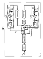
- FIG. 1 shows a configuration of a calibration unit of a conventional time-interleaved analog-digital converter cited from Non-Patent Document 1.
- Non-Patent Document 1 in a time-interleaved analog-digital converter composed of four unit analog-digital conversion units, the maximum value and DC offset value of the conversion output of each unit analog-digital conversion unit are calculated by digital calculation, The LMS (Least Mean Square) algorithm is used to convert the conversion gains and DC offset values of the remaining three unit analog-digital conversion units so that is equal to the maximum amplitude value and DC offset value of the output of the first unit analog-digital conversion unit.
- LMS Least Mean Square
- this method does not have a reference analog-digital converter that periodically notifies each unit analog-digital conversion unit of an accurate conversion result.
- the first analog-digital conversion unit is used as a reference analog-digital converter.
- the first unit analog-digital unit is different in sampling timing from the second, third, and fourth unit analog-digital conversion units due to the operation principle of the time interleave method, it is true as in Patent Document 1. It is not possible to serve as a reference analog-to-digital converter, and only “macro” information such as a maximum amplitude value and a DC offset can be notified.
- each unit analog-digital conversion unit cannot obtain a reference signal in units of one sample, fine correction cannot be performed.
- the maximum amplitude value of each unit analog-digital conversion unit is not necessarily the same in the first place, so the remaining maximum amplitude value of the first analog-digital conversion unit, as described above, Corrections that attempt to match the maximum amplitude values of the outputs of all analog-to-digital conversion units create errors.
- response time is required to obtain the maximum amplitude value. The convergence time of the LMS algorithm becomes long, or the tracking speed of the algorithm to the environmental change becomes slow.
- finer reference in sample units
- finer reference is necessary for correction such as sampling timing mismatch, nonlinearity mismatch, frequency characteristic mismatch, etc. Items that require information cannot be corrected.
- Patent Document 1 discloses a method of calibrating a time interleaved analog-digital converter using a reference analog-digital converter (described as a teacher analog-digital converter in the specification). Yes.
- each unit analog-digital conversion unit is synchronized with the reference analog-digital converter, so that a reference signal can be obtained in units of one sample.
- the reference analog-to-digital converter operates at the sample rate fCLK itself as the entire time-interleaved analog-to-digital converter, and thus operates at high speed when the parallel number M increases. Required.
- the bandwidth of the calibration algorithm it is necessary to reduce the bandwidth of the calibration algorithm, but this is nothing less than reducing the convergence of the calibration, so the degree of mismatch that can be tolerated by calibration
- the response time of the calibration is reduced, that is, the follow-up to the environmental change is delayed.
- the low-resolution reference analog-to-digital converter has not only large quantization noise but also large nonlinearity, but the latter effect can be avoided by simply reducing the bandwidth of the calibration algorithm. As a result, it is considered that the calibration accuracy is limited.
- the analog-to-digital converter of the present invention includes M unit analog-to-digital conversion units (M is an integer of 2 or more) connected in parallel with each other, and M units having different phases and the same sample rate.
- An analog-to-digital converter having a sample rate M times that of the unit analog-to-digital conversion unit, the reference analog-to-digital conversion units having a lower sample rate and higher resolution than the unit analog-to-digital conversion unit,
- M and N are disjoint and for reference Based on the output of the burner log-digital conversion unit, and having a function of performing calibration for each of the M unit analog-to-digital conversion unit.
- M unit analog-digital conversion units (M is an integer of 2 or more) having different phases and the same sample rate are connected in parallel to each other, and A semiconductor integrated circuit device in which an analog-digital converter having a sample rate M times that of the unit analog-digital conversion unit is formed on a single semiconductor substrate together with a clock source, wherein the analog-digital converter includes the unit A reference analog-digital conversion unit having a lower sample rate and higher resolution than the analog-digital conversion unit is connected in parallel to the M unit analog-digital conversion units, and the sample rate of the analog-digital converter is the reference Sample rate for analog to digital conversion unit If it is N times (N is an integer greater than or equal to 2), the M and the N are relatively prime and based on the output of the reference analog-to-digital conversion unit, the M unit analog digitals It has a function of performing calibration for each of the conversion units.
- a reference analog-to-digital conversion unit is connected in parallel to a common input to the time-interleaved analog-to-digital converter to be calibrated, and the reference analog-to-digital conversion unit outputs a low speed, Using the high-resolution analog-digital conversion results, the output of each unit analog-digital conversion unit that constitutes the time-interleaved analog-digital converter is post-calibrated in the digital domain, that is, each unit analog-digital to be calibrated Calibration is performed after the conversion unit (on the output side).
- the operation clock frequency of the above-mentioned reference analog-digital conversion unit is fCLK / N (where fCLK is the sample rate of the entire time-interleaved analog-digital converter. N is the parallel number M of the unit analog-digital conversion units)
- the digital calibration unit uses the conversion output supplied from the reference analog-to-digital converter as a reference signal that periodically tells the correct analog-to-digital conversion result of each unit analog-to-digital conversion unit. Can be corrected in the background during normal operation of the analog-to-digital converter. That is, according to the present invention, by appropriately selecting the operation clock frequency of the reference analog-digital converter, the operation clock of each unit analog-digital conversion unit can be operated even at an operation sufficiently lower than the sample rate of the time interleaved analog-digital converter as a whole. One feature is that it focuses on the fact that it can be synchronized sequentially with the edges. Further, the sampling timing of the unit analog-digital conversion unit is generated by an operation clock input to each of the M unit analog-digital conversion units. In this case, the sample rate corresponds to the operation clock frequency that is the frequency of the operation clock.
- FIG. 2 shows a first embodiment of the present invention.
- M is an integer of 2 or more
- unit analog-digital conversion unit 201 A / D / 1 to A / D M
- each subsequent digital calibration unit 202 CAL 1 to CAL
- M multiplexer
- a multiplexer 203 for sequentially taking in the output of each digital calibration unit
- a reference analog-to-digital conversion unit 204 connected to the input in parallel to each unit analog-to-digital conversion unit 202.
- Each unit analog-digital conversion unit 201 operates in the same manner as a normal time-interleaved analog-digital converter.
- the operation is performed at the operation CLK of the sampling CLK frequency fCLK / M, and each sampling timing is sequentially shifted by 1 / fCLK.
- the reference analog-digital conversion unit 204 operates at an operation CLK of fCLK / N.
- N is selected so that the sampling of each unit analog-digital conversion unit is periodically synchronized with the sampling of the reference analog-digital conversion unit 204.
- N can be selected so as to be relatively prime to the parallel number M of the unit analog-digital conversion unit 201.
- both the first analog-digital conversion unit and the second analog-digital conversion unit can synchronize with the sampling of the reference analog-digital converter 204 once every five samples.
- each digital calibration unit 202 can perform calibration using the conversion output of the reference analog-to-digital converter 204 as a reference signal.
- the DC offset voltage, conversion gain, and sampling timing of each unit analog-digital conversion unit are corrected to be equal to the DC offset voltage, conversion gain, and sampling timing of the reference analog-digital conversion unit 204. Mismatch between analog-digital conversion units is eliminated.
- FIG. 4 shows a configuration example of each digital calibration unit 202.
- the output from each unit analog-digital conversion unit 201 is converted by the conversion gain calibration unit 401 (Sub (LMS A), the DC offset calibration unit 402 (Sub LMS B) and the sampling timing calibration unit 403 (Sub LMS X), respectively.
- the conversion gain, the DC offset, and the sampling timing are corrected by, for example, the LMS algorithm so as to be equal to the conversion gain, the DC offset, and the sampling timing of the reference analog-to-digital conversion unit 204.
- a non-linearity calibration unit and a frequency characteristic calibration unit may be provided.
- a difference from the output of each digital calibration unit that is, a conversion error (e) is obtained using the conversion output of the reference analog-digital conversion unit 204 as a reference signal, and each calibration unit 401, 402 is obtained. , 403, etc.
- the former is down once every M times with the down sampler 404, and the latter is down once every N times with the down sampler 405.
- the subtraction unit 406 calculates the difference between the two as a conversion error.
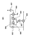
- the conversion gain calibration unit shown in FIG. 5 operates as follows. First, the sign of the conversion error (e) supplied as described above is inverted by the inversion unit 501. Further, the input signal to the conversion gain calibration unit is down-sampled once every N times in the down sampler 502 in order to synchronize. These two signals and the parameter ⁇ G that determines the transfer function of the loop are multiplied in a multiplier 503 and then integrated in an accumulator 506 composed of an adder 504 and a delay unit 505.
- This integrated output is rate-converted N times by the up-sampler 507 so as to be multiplied by the input signal to the conversion gain calibration unit in accordance with the rate, and is multiplied and output by the input signal and the multiplier 508.
- the conversion error (e) and the parameter ⁇ OFS determining the loop transfer function supplied by the above are multiplied in the multiplier 601, and then added by the adder 602 and the delay unit.
- an accumulator 604 composed of 603 integration is performed.
- This integrated output VOFS is rate-converted N times by the up-sampler 605 and subtracted by the subtractor 606 from the input signal to be subtracted in accordance with the rate of the input signal to the DC offset calibration unit.
- the sampling timing calibration unit shown in FIG. 7 operates as follows. In order to correct the sampling timing, it is necessary to obtain a skew ⁇ t between the sampling clock of the reference analog-digital conversion unit 204 and the sampling clock of each unit analog-digital conversion unit.
- the most important block is a block for deriving the time derivative of the input signal to the sampling timing calibration unit. In the present embodiment, this is an example in which this is most easily performed using a difference.
- the differentiator 701 includes a subtractor 702 and a one sample delay unit 703.
- the 1-sample delay unit 703 delays the input signal to the sampling timing calibration unit in the digital calibration unit following the unit analog-digital conversion unit that operates one sample before the unit analog-digital conversion unit.
- the difference of the input signal to the sampling timing calibration unit is derived by subtracting in the subtractor 702 from the input signal to the sampling timing calibration unit.
- This difference signal is down-sampled once every N times by the down sampler 704 in order to synchronize with the conversion error signal (e) supplied to the sampling timing calibration unit.
- the conversion error, the difference signal, and the parameter ⁇ skew that determines the transfer function of the loop are multiplied by a multiplier 705 and then integrated in an accumulator 708 including an adder 706 and a delay 707.
- This integrated output tskew is rate-converted N times by the upsampler 709 in order to match the rate with the input signal to the sampling timing calibration unit, multiplied by the difference signal and the multiplier 710, and then subtracted. In 711, it is subtracted from the input signal and output. If the sampling clock of a certain unit analog-digital conversion unit has a skew of ⁇ t with respect to the sampling clock of the reference analog-digital conversion unit 204, the output tskew of the accumulator 708 converges to ⁇ t, so that The mismatch of sampling timing can be absorbed by the equation shown in [Formula 1].
- FIG. 8 shows a timing chart of the present embodiment.
- the frequency of the operation clocks CLK1 and CLK2 of the first and second unit analog-digital conversion units is fCLK / 2
- the frequency of the operation clock CLKR of the reference analog-digital conversion unit 204 is fCLK / 5. It becomes.
- fCLK is a sample rate of the entire time interleave type analog-digital converter.
- the first unit analog-digital conversion unit and the second unit analog-digital conversion unit perform analog-to-digital conversion by sampling alternately, and sequentially output D1, D2, D3, D4,.
- the reference analog-to-digital conversion unit 204 performs sampling and analog-to-digital conversion at a rate 5/2 times slower than each unit analog-to-digital conversion unit, and sequentially outputs R1, R6, R11, R16,.
- the subscript R is matched to the sampling number of each unit analog-digital conversion unit with which the sampling timing is synchronized. In the example of this figure, since the outputs D1, D11, D21,...
- the conversion error e1 , E11, e21,... are calculated as described above, and are included in the conversion gain calibration unit, DC offset calibration unit, and sampling timing calibration unit in the first digital calibration unit as described above based on the result.
- the output of each accumulator, G1, VOFS1, and tskew1 is updated.
- G1, G2, VOFS1, VOFS2, tskew1, and tskew2 are automatically corrected by the LMS algorithm so that there is no mismatch with the reference analog-to-digital conversion unit 202. Thereby, each mismatch between the first unit analog-digital conversion unit and the second unit analog-digital conversion unit is also eliminated.
- the time interleave type analog-digital converter can perform high-accuracy calibration corresponding to the high-speed sample rate of the next generation application and realizing high resolution.
- FIG. 9 shows a second embodiment of the present invention.
- the time differentiator used in the part is replaced with a more accurate time differentiator from the simple differentiator as in the first embodiment.
- a delay unit 911 for K / 2 samples is required.
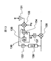
- the conversion gain calibration units 903 and 904 have the configuration shown in FIG. In FIG.
- a delay unit 139 for K / 2 samples is still required to compensate for the delay time for K / 2 samples generated in the time differentiator, but the operation is the same as described in the first embodiment. It is.
- the sampling timing calibration units 907 and 908 of FIG. 9 have the configuration of FIG. In this configuration, the difference from the sampling timing calibration unit (FIG. 7) in the first embodiment is that a high-precision time differentiator 101 and a time second-order differentiator 102 are introduced, and the reference analog-to-digital conversion unit is The sampling timing skew ⁇ t between the unit analog-digital conversion units is corrected with higher accuracy than in the first embodiment.
- the multiplier 1010 and the subtractor 1013 correct the third item of the equation shown in [Expression 2] above.
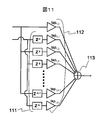
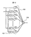
- the configurations of the time differentiator 101 and the time second-order differentiator 102 are shown in FIGS. 11 and 12, respectively. Both can be realized as an FIR filter composed of a finite number of taps, and include delay units 111 and 121, multipliers 112 and 122 using tap coefficients, and adders 113 and 123 for adding the multiplication results.
- the upper input is from the unit analog-digital conversion unit
- the lower input is from the remaining one unit analog-digital conversion unit. Each input is connected to each tap every two taps.
- the number M of unit analog-digital conversion units is 2.
- M 3
- the number of inputs is 3, and the top is the second from the unit analog-digital conversion unit. Is input from the unit analog-digital conversion unit that samples one unit before the unit analog-digital conversion unit, and the third is input from the unit analog-digital conversion unit that samples two units before the unit analog-digital conversion unit. Will be connected to each tap every 3 taps.
- M general
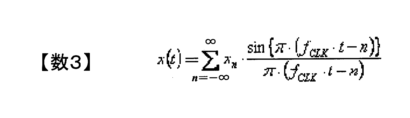
- the tap coefficient tap1, i of the time differentiator (FIG. 11) and the tap coefficient tap2, i of the time second-order differentiator (FIG. 12) are expressed by the sampling theorem shown in [Equation 3] below as 1
- the second order differentiation and the second order differentiation it can be derived as the following equations [Formula 4] to [Formula 7].
- the number of taps of the FIR filter is K + 1.
- K is a multiple of 4.
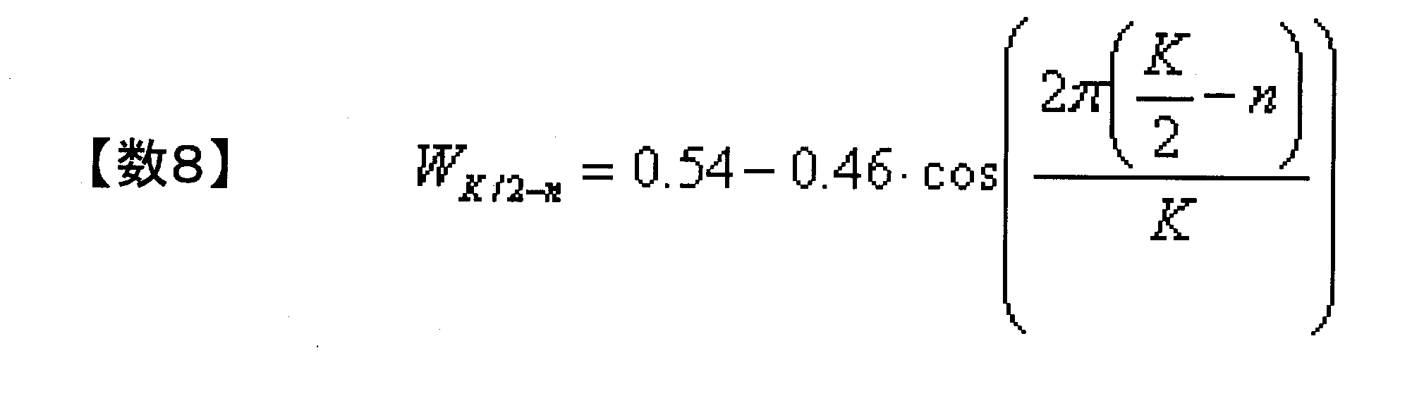
- the tap coefficient of [Equation 4] to [Equation 7] is finally multiplied by the window function of [Equation 8], for example.
- FIG. 14 shows an operation timing chart of this embodiment.
- the time interleave type analog-digital converter can perform high-accuracy calibration corresponding to the high-speed sample rate of the next generation application and realizing high resolution.
- FIG. 15 shows a third embodiment of the present invention.
- the sampling timing calibration unit is further improved in accuracy in the second embodiment.
- the sampling timing calibration units 157 and 158 are configured by serially connecting the configuration of FIG. 10 described in the second embodiment and a configuration similar to that (FIG. 16). Accordingly, a delay corresponding to K samples occurs in the above-described sampling timing calibration units 157 and 158, and is compensated by the K sample delay unit 161 in FIG.
- the sampling timing is corrected with extremely high accuracy. There are limitations.
- the present embodiment first, in the configuration of FIG.
- FIG. 10 similarly to the second embodiment, after correcting the skew mismatch to improve the signal quality, in the configuration of FIG.
- the sampling timing calibration unit increases the correction accuracy with the two-stage configuration as described above. However, it is considered that the correction accuracy can be further improved by extending this to three or more stages.
- the conversion gain calibration units 153 and 154 in FIG. 15 have the configuration as shown in FIG. 17, but the delay amount of the delay unit for compensating for the delay time generated in the time differentiator and second time differentiator. Except for the differences, the operation is basically the same as the example shown in FIGS. 5 and 13, and the detailed description is omitted.
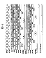
- FIG. 18 shows an operation timing chart of this embodiment.
- the time interleave type analog-digital converter can perform high-accuracy calibration corresponding to the high-speed sample rate of the next generation application and realizing high resolution.
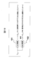
- FIG. 19 shows a configuration example of the CLK generator as the fourth embodiment of the present invention.
- This example is the most general example.
- the fCLK / M frequency clock signal required by each unit analog-digital conversion unit and the fCLK / N frequency clock signal required by the reference analog-digital conversion unit are generated to generate the source CLK signal of frequency fCLK.
- This configuration requires a source CLK signal having a frequency equal to the sample rate fCLK for the entire time interleaved analog-digital converter, but the rising edge of the output of the N divider 191 and the rising edge of the output of the M divider 192. Since both edges operate only at the rising edge of the source CLK signal, the skew is always a constant value, and the above-described calibration of the sampling timing functions most effectively.
- the time interleave type analog-digital converter can perform high-accuracy calibration corresponding to the high-speed sample rate of the next generation application and realizing high resolution.
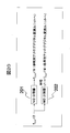
- FIG. 20 shows another example of the configuration of the CLK generator as the fifth embodiment of the present invention.
- the frequency of the source CLK signal is fCLK / 2. Therefore, in order to generate the clock signal having the fCLK / M frequency required by each unit analog-digital conversion unit and the clock signal having the fCLK / N frequency required by the reference analog-digital conversion unit, the source CLK signal is generated.
- the frequency is divided by the N / 2 frequency divider 201 and the M / 2 frequency divider 202, respectively, and the former output is supplied to the reference analog-digital conversion unit, and the latter output is supplied to each unit analog-digital conversion unit.
- This configuration may be a source CLK signal having a frequency that is half the sample rate fCLK of the entire time interleaved analog-digital converter, but the rising edge of the output of the N / 2 divider 201 or the M / 2 divider 202
- N or M is an odd number
- the rising edge of the output operates alternately at the rising edge and the falling edge of the source CLK signal. Therefore, when the source CLK signal is not strictly duty ratio 50%, these frequency dividers
- the output skew will oscillate, and there may be some limitations on the calibration of the sampling timing. However, as described above, since N and M are relatively prime, one of them is at least an odd number, and this state is obtained.
- the time interleave type analog-digital converter can perform high-accuracy calibration corresponding to the high-speed sample rate of the next generation application and realizing high resolution.
- FIG. 21 shows still another configuration example of the CLK generator as the sixth embodiment of the present invention.
- the frequency of the source CLK signal is reduced to fCLK / N required by the reference analog-digital conversion unit. Therefore, a clock signal having a frequency of fCLK / M required by each unit analog-digital conversion unit is obtained as follows. First, the source CLK signal having the frequency fCLK / N is divided by the M frequency divider 211 to obtain the CLK signal having the frequency fCLK / N / M. This signal is input to an N * M tap DLL (Delay Locked Loop) circuit 212, and an N * M phase output having a time difference of 1 / fCLK is obtained.
- N * M tap DLL Delay Locked Loop
- the time interleave type analog-digital converter can perform high-accuracy calibration corresponding to the high-speed sample rate of the next generation application and realizing high resolution.
- FIG. 22 shows a seventh embodiment of the present invention.
- a layout example of a chip for demonstrating the effectiveness of the present invention is shown.
- M is not limited to a specific number as long as it is an integer of 2 or more.
- each of the unit analog-digital conversion units A / D1 to A / D7 and the reference analog-digital conversion unit Ref A / D are formed on a single semiconductor substrate together with a clock source to constitute a semiconductor integrated circuit chip.
- Each of the unit analog-digital conversion units A / D1 to A / D7 and the reference analog-digital conversion unit Ref A / D are densely arranged so that a gap portion where these are not arranged is minimized.
- the layout includes a combination of units having different distances from the clock source to each unit analog-digital conversion unit and the reference analog-digital conversion unit.
- the influence of the skew of the sampling CLK between the unit analog-digital conversion units can be removed by calibration. Therefore, the CLK wiring is usually made equal in length, and the arrangement configuration suitable for this purpose is also provided. Is not required for each unit analog-digital conversion unit.
- the layout area is minimized, that is, the chip cost is minimized without being affected by the difference in wiring length between each unit analog-digital conversion unit and the reference analog-digital conversion unit.
- each unit analog-digital conversion unit and reference analog-digital conversion unit can be optimally arranged. In other words, a layout that avoids an increase in layout area due to a useless space in which it is difficult to arrange other circuit blocks is possible.
- FIG. 23 shows an eighth embodiment of the present invention.
- a chip layout example different from that of the seventh embodiment is shown.
- M is not limited to a specific number as long as it is an integer of 2 or more.
- each unit analog-digital conversion unit and reference analog-digital conversion In the case of the prior art in which the sampling timing is not calibrated, the CLK wiring to each unit analog-digital conversion unit needs to be an equal length wiring.
- each unit analog-digital conversion unit and reference analog-digital conversion Although there were restrictions on the layout such that the units need to be arranged in a circle centered on the clock source, even if the calibration of the present invention is applied, the equal length CLK wiring arrangement such as this circle arrangement Can be applied as in the conventional case.
- each of the unit analog-digital conversion units A / D1 to A / D7 and the reference analog-digital conversion unit Ref A / D are formed on a single semiconductor substrate together with a clock source to constitute a semiconductor integrated circuit chip. .
- Each of the unit analog-digital conversion units A / D1 to A / D7 and the reference analog-digital conversion unit Ref A / D are arranged in a circle so that the distances from the clock source are substantially equal to each other.
- the gap portion where the unit analog-digital conversion units A / D1 to A / D7 and the reference analog-digital conversion unit Ref A / D are not arranged is not minimized, and so is a sparse arrangement.
- a signal in which the influence of the CLK skew is reduced to some extent by the equal-length wiring is input to each unit analog-digital conversion unit and reference analog-digital conversion unit.
- the influence of the sampling CLK skew is reduced to some extent by the equal-length wiring, and then the calibration of the present invention is applied, thereby reducing the calibration load on each unit analog-digital conversion unit. Is possible. In addition, it is particularly effective for applications under severe conditions that are different from normal cases where the effects of the skew of sampling CLK between each unit analog-digital conversion unit and the reference analog-digital conversion unit cannot be completely removed by calibration alone. is there.
Landscapes
- Engineering & Computer Science (AREA)
- Theoretical Computer Science (AREA)
- Analogue/Digital Conversion (AREA)
Abstract
Description
C Hsu(C. Hsu et al., "An 11b 800MS/s time-interleaved ADC with digital background calibration," 2007 IEEE International Solid State Circuits Conference (ISSCC), Session 25.7, pp. 464-465(2007).)






Claims (20)
- 位相が互いに異なりかつサンプルレートが互いに等しいM個の単位アナログデジタル変換ユニット(Mは2以上の整数である)が互いに並列に接続されてなり、かつ、前記単位アナログデジタル変換ユニットのM倍のサンプルレートを有するアナログデジタル変換器であって、
前記単位アナログデジタル変換ユニットよりもサンプルレートが低くかつ分解能が高い参照用アナログデジタル変換ユニットが、前記M個の単位アナログデジタル変換ユニットに対して並列に接続され、
前記アナログデジタル変換器のサンプルレートが前記参照用アナログデジタル変換ユニットのサンプルレートのN倍である(Nは2以上の整数である)とした場合、前記Mと前記Nとは互いに素であり、
前記参照用アナログデジタル変換ユニットの出力に基づいて、前記M個の単位アナログデジタル変換ユニットの各々に対するキャリブレーションを行う機能を有する
ことを特徴とするアナログデジタル変換器。 - 請求項1において、
前記キャリブレーションは、前記M個の単位アナログデジタル変換ユニットの各々の出力に対してデジタル領域で行うポストキャリブレーションである
ことを特徴とするアナログデジタル変換器。 - 請求項2において、
前記ポストキャリブレーションは、前記アナログデジタル変換器の通常動作中にバックグランドで実行される
ことを特徴とするアナログデジタル変換器。 - 請求項1において、
前記単位アナログデジタル変換ユニットのサンプリングのタイミングは前記M個の単位アナログデジタル変換ユニットの各々に入力される動作クロックによって生成され、
前記サンプルレートは前記動作クロックの周波数である動作クロック周波数に対応する
ことを特徴とするアナログデジタル変換器。 - タイムインターリーブ型のアナログデジタル変換器であって、
入力に対して並列に、参照用アナログデジタル変換ユニットが接続され、
前記参照用アナログデジタル変換ユニットの変換出力を利用して、デジタルキャリブレーションにより、前記タイムインターリーブ型のアナログデジタル変換器を構成する各単位アナログデジタル変換ユニット間の変換利得のミスマッチ、DCオフセット電圧のミスマッチ、サンプリングタイミングのミスマッチ、非線形性のミスマッチ、および周波数特性のミスマッチの少なくとも1つを補正するよう構成され、
前記参照用アナログデジタル変換ユニットの動作クロック周波数は、前記タイムインターリーブ型のアナログデジタル変換器全体としてのサンプルレートより小さく、かつ、前記各単位アナログデジタル変換ユニットのサンプリングに順次同期するように設定される
ことを特徴とするアナログデジタル変換器。 - 請求項5において、
前記デジタルキャリブレーションのアルゴリズムとして、LMS(Least Mean Square)アルゴリズムが適用されて成る
ことを特徴とするアナログデジタル変換器。 - 請求項5において、
前記参照用アナログデジタル変換ユニットの動作クロック周波数は、前記タイムインターリーブ型のアナログデジタル変換器全体としてのサンプルレートの1/Nに設定され、
前記Nは、前記タイムインターリーブ型のアナログデジタル変換器を構成する単位アナログデジタル変換ユニットの並列数Mと互いに素である
ことを特徴とするアナログデジタル変換器。 - 請求項5において、
前記参照用アナログデジタル変換ユニットの動作クロック周波数は、前記各単位アナログデジタル変換ユニットの動作クロック周波数より小さく設定される
ことを特徴とするアナログデジタル変換器。 - 請求項5において、
前記サンプリングタイミングのミスマッチを補正するために、前記デジタルキャリブレーションを時間の1階微分器によって行う
ことを特徴とするアナログデジタル変換器。 - 請求項9において、
前記1階微分器として、サンプリング定理と窓関数とから求まる固定のタップ係数を持つFIRフィルタが用いられる
ことを特徴とするアナログデジタル変換器。 - 請求項5において、
前記サンプリングタイミングのミスマッチを補正するために、前記デジタルキャリブレーションを時間の2階以上の微分器によって行う
ことを特徴とするアナログデジタル変換器。 - 請求項11において、
前記2階以上の微分器として、サンプリング定理と窓関数とから求まる固定のタップ係数を持つFIRフィルタが用いられる
ことを特徴とするアナログデジタル変換器。 - 請求項5において、
前記サンプリングタイミングのミスマッチを補正するために、前記サンプリングタイミングのキャリブレーションを行う手段が複数段従属接続されて成る
ことを特徴とするアナログデジタル変換器。 - 請求項5において、
前記参照用アナログデジタル変換ユニットの動作クロック周波数および前記各単位アナログデジタル変換ユニットの動作クロック周波数の少なくとも一方は、(奇数/2)分周器を用いて生成される
ことを特徴とするアナログデジタル変換器。 - 請求項5において、
前記参照用アナログデジタル変換ユニットの動作クロック周波数および前記各単位アナログデジタル変換ユニットの動作クロック周波数の少なくとも一方は、DLL(Delay Locked Loop)回路とエッジコンバイナー(Edge Combiner)回路とを用いて生成される
ことを特徴とするアナログデジタル変換器。 - 位相が互いに異なりかつサンプルレートが互いに等しいM個の単位アナログデジタル変換ユニット(Mは2以上の整数である)が互いに並列に接続されてなり、かつ、前記単位アナログデジタル変換ユニットのM倍のサンプルレートを有するアナログデジタル変換器がクロック源と共に単一の半導体基板上に形成されて成る半導体集積回路装置であって、
前記アナログデジタル変換器は、
前記単位アナログデジタル変換ユニットよりもサンプルレートが低くかつ分解能が高い参照用アナログデジタル変換ユニットが、前記M個の単位アナログデジタル変換ユニットに対して並列に接続され、
前記アナログデジタル変換器のサンプルレートが前記参照用アナログデジタル変換ユニットのサンプルレートのN倍である(Nは2以上の整数である)とした場合、前記Mと前記Nとは互いに素であり、
前記参照用アナログデジタル変換ユニットの出力に基づいて、前記M個の単位アナログデジタル変換ユニットの各々に対するキャリブレーションを行う機能を有する
ことを特徴とする半導体集積回路装置。 - 請求項16において、
前記キャリブレーションは、前記M個の単位アナログデジタル変換ユニットの各々の出力に対してデジタル領域で行うポストキャリブレーションである
ことを特徴とする半導体集積回路装置。 - 請求項17において、
前記ポストキャリブレーションは、前記アナログデジタル変換器の通常動作中にバックグランドで実行される
ことを特徴とする半導体集積回路装置。 - 請求項16において、
前記単位アナログデジタル変換ユニットのサンプリングのタイミングは前記M個の単位アナログデジタル変換ユニットの各々に入力される動作クロックによって生成され、
前記サンプルレートは前記動作クロックの周波数である動作クロック周波数に対応する
ことを特徴とする半導体集積回路装置。 - 請求項16において、
前記各単位アナログデジタル変換ユニットおよび前記参照用アナログデジタル変換ユニットは、前記各単位アナログデジタル変換ユニットも前記参照用アナログデジタル変換ユニットも配置されない隙間の部分が最小となるように配置され、
前記クロック源から前記各単位アナログデジタル変換ユニットおよび前記参照用アナログデジタル変換ユニットまでの距離が互いに異なるユニット同士の組合せが存在する
ことを特徴とする半導体集積回路装置。
Priority Applications (5)
| Application Number | Priority Date | Filing Date | Title |
|---|---|---|---|
| PCT/JP2009/052870 WO2010095232A1 (ja) | 2009-02-19 | 2009-02-19 | アナログデジタル変換器および半導体集積回路装置 |
| US12/676,357 US8102289B2 (en) | 2009-02-19 | 2009-02-19 | Analog/digital converter and semiconductor integrated circuit device |
| JP2011500395A JP5095007B2 (ja) | 2009-02-19 | 2009-02-19 | アナログデジタル変換器および半導体集積回路装置 |
| US13/338,338 US8736470B2 (en) | 2009-02-19 | 2011-12-28 | Analog/digital converter and semiconductor integrated circuit device |
| US14/265,762 US8922407B2 (en) | 2009-02-19 | 2014-04-30 | Analog/digital converter and semiconductor integrated circuit device |
Applications Claiming Priority (1)
| Application Number | Priority Date | Filing Date | Title |
|---|---|---|---|
| PCT/JP2009/052870 WO2010095232A1 (ja) | 2009-02-19 | 2009-02-19 | アナログデジタル変換器および半導体集積回路装置 |
Related Child Applications (2)
| Application Number | Title | Priority Date | Filing Date |
|---|---|---|---|
| US12/676,357 A-371-Of-International US8102289B2 (en) | 2009-02-19 | 2009-02-19 | Analog/digital converter and semiconductor integrated circuit device |
| US13/338,338 Continuation US8736470B2 (en) | 2009-02-19 | 2011-12-28 | Analog/digital converter and semiconductor integrated circuit device |
Publications (1)
| Publication Number | Publication Date |
|---|---|
| WO2010095232A1 true WO2010095232A1 (ja) | 2010-08-26 |
Family
ID=42633533
Family Applications (1)
| Application Number | Title | Priority Date | Filing Date |
|---|---|---|---|
| PCT/JP2009/052870 Ceased WO2010095232A1 (ja) | 2009-02-19 | 2009-02-19 | アナログデジタル変換器および半導体集積回路装置 |
Country Status (3)
| Country | Link |
|---|---|
| US (3) | US8102289B2 (ja) |
| JP (1) | JP5095007B2 (ja) |
| WO (1) | WO2010095232A1 (ja) |
Cited By (10)
| Publication number | Priority date | Publication date | Assignee | Title |
|---|---|---|---|---|
| JP2011044920A (ja) * | 2009-08-21 | 2011-03-03 | Denso Corp | Ad変換装置 |
| JP2011049746A (ja) * | 2009-08-26 | 2011-03-10 | Nec Corp | A/d変換装置 |
| JP2011097215A (ja) * | 2009-10-28 | 2011-05-12 | Nec Corp | A/d変換装置 |
| CN102739252A (zh) * | 2011-04-12 | 2012-10-17 | 美信集成产品公司 | 用于时间交织模数转换器的后台校准的系统和方法 |
| JP5836493B2 (ja) * | 2012-09-07 | 2015-12-24 | 株式会社日立製作所 | インターリーブa/d変換器 |
| US9287889B2 (en) | 2014-04-17 | 2016-03-15 | The Board Of Regents, The University Of Texas System | System and method for dynamic path-mismatch equalization in time-interleaved ADC |
| JP2017147637A (ja) * | 2016-02-18 | 2017-08-24 | 日本電波工業株式会社 | 信号処理装置 |
| JP2017153075A (ja) * | 2016-02-25 | 2017-08-31 | ザ・ボーイング・カンパニーThe Boeing Company | 耐放射線強化インターリーブアナログ−デジタル変換回路及びその較正方法 |
| JP2018524874A (ja) * | 2015-06-11 | 2018-08-30 | アプライド・マイクロ・サーキット・コーポレーション | 受信機の較正および追跡 |
| KR20220007639A (ko) * | 2019-05-10 | 2022-01-18 | 웨스팅하우스 일렉트릭 컴퍼니 엘엘씨 | 교정 시스템 및 방법 |
Families Citing this family (17)
| Publication number | Priority date | Publication date | Assignee | Title |
|---|---|---|---|---|
| US5861147A (en) | 1997-06-09 | 1999-01-19 | The Procter & Gamble Company | Methods for controlling environmental odors on the body using compositions comprising uncomplexed cyclodextrins and perfume |
| KR101012678B1 (ko) * | 2009-02-04 | 2011-02-09 | 연세대학교 산학협력단 | 지연 동기 루프 및 이를 포함하는 전자 장치 |
| US8102289B2 (en) * | 2009-02-19 | 2012-01-24 | Hitachi, Ltd. | Analog/digital converter and semiconductor integrated circuit device |
| US8564462B2 (en) | 2010-09-08 | 2013-10-22 | Broadcom Corporation | Digital correction techniques for data converters |
| JP5733027B2 (ja) * | 2011-05-31 | 2015-06-10 | ソニー株式会社 | Ad変換装置および信号処理システム |
| US9030341B2 (en) * | 2012-06-27 | 2015-05-12 | Broadcom Corporation | Compensation for lane imbalance in a multi-lane analog-to-digital converter (ADC) |
| US9178625B1 (en) * | 2012-12-03 | 2015-11-03 | Clariphy Communications Inc. | Timing recovery for optical coherent receivers in the presence of polarization mode dispersion |
| JP6230417B2 (ja) | 2013-12-27 | 2017-11-15 | ルネサスエレクトロニクス株式会社 | A/d変換回路および半導体集積回路 |
| US9214951B1 (en) * | 2014-05-30 | 2015-12-15 | Realtek Semiconductor Corp. | Self-calibrating VCO-based analog-to-digital converter and method thereof |
| US9806735B2 (en) * | 2015-01-13 | 2017-10-31 | Texas Instruments Incorporated | High speed data transfer for analog-to-digital converters |
| CN106130551A (zh) | 2015-05-07 | 2016-11-16 | 松下知识产权经营株式会社 | A/d 转换器 |
| CN107852166B (zh) * | 2015-09-07 | 2020-09-25 | 华为技术有限公司 | 并行重采样器 |
| CN110504969B (zh) * | 2018-05-18 | 2023-03-24 | 创意电子股份有限公司 | 模拟数字转换器装置与待测信号产生方法 |
| TWI693799B (zh) * | 2019-01-23 | 2020-05-11 | 創意電子股份有限公司 | 類比數位轉換器裝置與時脈偏斜校正方法 |
| US10742226B1 (en) * | 2019-06-17 | 2020-08-11 | The 58Th Research Institute Of China Electronics Technology Group Corporation | Multi-channel high-precision ADC circuit with self-calibration of mismatch error |
| US11552646B2 (en) | 2020-06-24 | 2023-01-10 | Stmicroelectronics International N.V. | Timing skew mismatch calibration for time interleaved analog to digital converters |
| JP7809558B2 (ja) | 2022-03-16 | 2026-02-02 | キオクシア株式会社 | 半導体集積回路、受信装置、及び受信方法 |
Citations (3)
| Publication number | Priority date | Publication date | Assignee | Title |
|---|---|---|---|---|
| JP2006313162A (ja) * | 2005-05-03 | 2006-11-16 | Agilent Technol Inc | 時間インターリーブされたデータコンバータのタイミングを較正するためのシステム及び方法 |
| WO2006126672A1 (ja) * | 2005-05-26 | 2006-11-30 | Advantest Corporation | アナログデジタル変換装置、プログラム、及び記録媒体 |
| JP2007150640A (ja) * | 2005-11-28 | 2007-06-14 | Hitachi Communication Technologies Ltd | 時間インターリーブad変換器 |
Family Cites Families (8)
| Publication number | Priority date | Publication date | Assignee | Title |
|---|---|---|---|---|
| US4763105A (en) * | 1987-07-08 | 1988-08-09 | Tektronix, Inc. | Interleaved digitizer array with calibrated sample timing |
| JP3161481B2 (ja) * | 1992-03-26 | 2001-04-25 | 岩崎通信機株式会社 | インターリーブ方式のa/dコンバータのオフセット補償回路 |
| US5294926A (en) * | 1992-10-09 | 1994-03-15 | Hewlett-Packard Company | Timing and amplitude error estimation for time-interleaved analog-to-digital converters |
| US6081215A (en) * | 1998-07-06 | 2000-06-27 | Motorola, Inc. | High speed interlaced analog interface |
| JP2003133954A (ja) * | 2001-10-26 | 2003-05-09 | Agilent Technologies Japan Ltd | インターリーブa/d変換器の校正方法 |
| EP1401105B1 (en) * | 2002-09-17 | 2006-06-14 | Siemens Mobile Communications S.p.A. | Voltage offset compensation method for time-interleaved multi-path analog-to-digital sigma-delta converters and respective circuit |
| JP3984284B2 (ja) * | 2005-01-11 | 2007-10-03 | アンリツ株式会社 | 改良された時間インタリーブ方式のアナログ−デジタル変換装置及びそれを用いる高速信号処理システム |
| US8102289B2 (en) * | 2009-02-19 | 2012-01-24 | Hitachi, Ltd. | Analog/digital converter and semiconductor integrated circuit device |
-
2009
- 2009-02-19 US US12/676,357 patent/US8102289B2/en not_active Expired - Fee Related
- 2009-02-19 WO PCT/JP2009/052870 patent/WO2010095232A1/ja not_active Ceased
- 2009-02-19 JP JP2011500395A patent/JP5095007B2/ja not_active Expired - Fee Related
-
2011
- 2011-12-28 US US13/338,338 patent/US8736470B2/en active Active
-
2014
- 2014-04-30 US US14/265,762 patent/US8922407B2/en not_active Expired - Fee Related
Patent Citations (3)
| Publication number | Priority date | Publication date | Assignee | Title |
|---|---|---|---|---|
| JP2006313162A (ja) * | 2005-05-03 | 2006-11-16 | Agilent Technol Inc | 時間インターリーブされたデータコンバータのタイミングを較正するためのシステム及び方法 |
| WO2006126672A1 (ja) * | 2005-05-26 | 2006-11-30 | Advantest Corporation | アナログデジタル変換装置、プログラム、及び記録媒体 |
| JP2007150640A (ja) * | 2005-11-28 | 2007-06-14 | Hitachi Communication Technologies Ltd | 時間インターリーブad変換器 |
Cited By (14)
| Publication number | Priority date | Publication date | Assignee | Title |
|---|---|---|---|---|
| JP2011044920A (ja) * | 2009-08-21 | 2011-03-03 | Denso Corp | Ad変換装置 |
| JP2011049746A (ja) * | 2009-08-26 | 2011-03-10 | Nec Corp | A/d変換装置 |
| JP2011097215A (ja) * | 2009-10-28 | 2011-05-12 | Nec Corp | A/d変換装置 |
| CN102739252A (zh) * | 2011-04-12 | 2012-10-17 | 美信集成产品公司 | 用于时间交织模数转换器的后台校准的系统和方法 |
| US9337853B2 (en) | 2012-09-07 | 2016-05-10 | Hitachi, Ltd. | Interleaved A/D converter |
| JP5836493B2 (ja) * | 2012-09-07 | 2015-12-24 | 株式会社日立製作所 | インターリーブa/d変換器 |
| US9287889B2 (en) | 2014-04-17 | 2016-03-15 | The Board Of Regents, The University Of Texas System | System and method for dynamic path-mismatch equalization in time-interleaved ADC |
| JP2018524874A (ja) * | 2015-06-11 | 2018-08-30 | アプライド・マイクロ・サーキット・コーポレーション | 受信機の較正および追跡 |
| JP2017147637A (ja) * | 2016-02-18 | 2017-08-24 | 日本電波工業株式会社 | 信号処理装置 |
| JP2017153075A (ja) * | 2016-02-25 | 2017-08-31 | ザ・ボーイング・カンパニーThe Boeing Company | 耐放射線強化インターリーブアナログ−デジタル変換回路及びその較正方法 |
| KR20220007639A (ko) * | 2019-05-10 | 2022-01-18 | 웨스팅하우스 일렉트릭 컴퍼니 엘엘씨 | 교정 시스템 및 방법 |
| JP2022533576A (ja) * | 2019-05-10 | 2022-07-25 | ウェスティングハウス エレクトリック カンパニー エルエルシー | 較正システム及び方法 |
| JP7661239B2 (ja) | 2019-05-10 | 2025-04-14 | ウェスティングハウス エレクトリック カンパニー エルエルシー | 較正システム、電子装置、及び、較正検証方法 |
| KR102870209B1 (ko) * | 2019-05-10 | 2025-10-14 | 웨스팅하우스 일렉트릭 컴퍼니 엘엘씨 | 교정 시스템 및 방법 |
Also Published As
| Publication number | Publication date |
|---|---|
| JPWO2010095232A1 (ja) | 2012-08-16 |
| US20140232578A1 (en) | 2014-08-21 |
| US20110128171A1 (en) | 2011-06-02 |
| US8736470B2 (en) | 2014-05-27 |
| US20130049999A1 (en) | 2013-02-28 |
| US8922407B2 (en) | 2014-12-30 |
| JP5095007B2 (ja) | 2012-12-12 |
| US8102289B2 (en) | 2012-01-24 |
Similar Documents
| Publication | Publication Date | Title |
|---|---|---|
| JP5095007B2 (ja) | アナログデジタル変換器および半導体集積回路装置 | |
| US7227479B1 (en) | Digital background calibration for time-interlaced analog-to-digital converters | |
| US7834786B2 (en) | Sample hold circuit for use in time-interleaved A/D converter apparatus including paralleled low-speed pipeline A/D converters | |
| Matsuno et al. | All-digital background calibration technique for time-interleaved ADC using pseudo aliasing signal | |
| US7324038B2 (en) | Subranging analog to digital converter with multi-phase clock timing | |
| JP5288003B2 (ja) | A/d変換装置とその補正制御方法 | |
| US20120262318A1 (en) | System and Method for Background Calibration of Time Interleaved Analog to Digital Converters | |
| JP5142342B2 (ja) | Ad変換回路 | |
| US8564462B2 (en) | Digital correction techniques for data converters | |
| EP3993272B1 (en) | Analog-to-digital converter system using reference analog-to-digital converter with sampling point shifting and associated calibration method | |
| JP2008515341A (ja) | 周波数合成の方法と装置 | |
| WO2014038056A1 (ja) | インターリーブa/d変換器 | |
| US11177822B2 (en) | System and method for background calibration of time interleaved ADC | |
| JPWO2011118370A1 (ja) | 時間インターリーブ方式a/d変換装置 | |
| JP5286420B2 (ja) | アナログデジタル変換器およびそれを用いた半導体集積回路装置 | |
| US8217691B2 (en) | Low power clocking scheme for a pipelined ADC | |
| KR100850747B1 (ko) | 알고리즘 아날로그-디지털 변환기 | |
| Mafi et al. | Background calibration of time-interleaved adcs with polyphase filters | |
| US20240007120A1 (en) | Time-Interleaved ADC | |
| KR102844404B1 (ko) | 타임 인터리브 아날로그 디지털 변환기를 위한 부분지연 fir 필터 기반의 백그라운드 타이밍 오차 보정 기법 | |
| Mafi et al. | Utilization of Noise-Shaping in Mixed-Signal Timing-Skew Mismatch Calibration of TI-ADCs | |
| Lee et al. | Calibration of time-skew error in a M-channel time-interleaved analog-to-digital converter | |
| CN120185607A (zh) | 一种时间交织模数转换器及其误差校准方法 |
Legal Events
| Date | Code | Title | Description |
|---|---|---|---|
| WWE | Wipo information: entry into national phase |
Ref document number: 12676357 Country of ref document: US |
|
| 121 | Ep: the epo has been informed by wipo that ep was designated in this application |
Ref document number: 09840339 Country of ref document: EP Kind code of ref document: A1 |
|
| WWE | Wipo information: entry into national phase |
Ref document number: 2011500395 Country of ref document: JP |
|
| NENP | Non-entry into the national phase |
Ref country code: DE |
|
| 122 | Ep: pct application non-entry in european phase |
Ref document number: 09840339 Country of ref document: EP Kind code of ref document: A1 |