US7324038B2 - Subranging analog to digital converter with multi-phase clock timing - Google Patents
Subranging analog to digital converter with multi-phase clock timing Download PDFInfo
- Publication number
- US7324038B2 US7324038B2 US10/625,702 US62570203A US7324038B2 US 7324038 B2 US7324038 B2 US 7324038B2 US 62570203 A US62570203 A US 62570203A US 7324038 B2 US7324038 B2 US 7324038B2
- Authority
- US
- United States
- Prior art keywords
- amplifier
- coarse
- analog
- digital converter
- clock phase
- Prior art date
- Legal status (The legal status is an assumption and is not a legal conclusion. Google has not performed a legal analysis and makes no representation as to the accuracy of the status listed.)
- Expired - Lifetime, expires
Links
- 239000003990 capacitor Substances 0.000 claims abstract description 58
- 239000011159 matrix material Substances 0.000 claims abstract description 12
- 230000003111 delayed effect Effects 0.000 claims description 12
- 230000005669 field effect Effects 0.000 claims description 2
- 230000000630 rising effect Effects 0.000 description 11
- 238000013139 quantization Methods 0.000 description 10
- 238000000034 method Methods 0.000 description 6
- 238000010586 diagram Methods 0.000 description 5
- 238000012935 Averaging Methods 0.000 description 2
- 238000005070 sampling Methods 0.000 description 2
- 230000003321 amplification Effects 0.000 description 1
- 238000003491 array Methods 0.000 description 1
- 238000006243 chemical reaction Methods 0.000 description 1
- 238000005259 measurement Methods 0.000 description 1
- 238000003199 nucleic acid amplification method Methods 0.000 description 1
Images


Classifications
-
- H—ELECTRICITY
- H03—ELECTRONIC CIRCUITRY
- H03M—CODING; DECODING; CODE CONVERSION IN GENERAL
- H03M1/00—Analogue/digital conversion; Digital/analogue conversion
- H03M1/12—Analogue/digital converters
- H03M1/14—Conversion in steps with each step involving the same or a different conversion means and delivering more than one bit
- H03M1/145—Conversion in steps with each step involving the same or a different conversion means and delivering more than one bit the steps being performed sequentially in series-connected stages
- H03M1/146—Conversion in steps with each step involving the same or a different conversion means and delivering more than one bit the steps being performed sequentially in series-connected stages all stages being simultaneous converters
-
- H—ELECTRICITY
- H03—ELECTRONIC CIRCUITRY
- H03K—PULSE TECHNIQUE
- H03K17/00—Electronic switching or gating, i.e. not by contact-making and –breaking
- H03K17/04—Modifications for accelerating switching
- H03K17/041—Modifications for accelerating switching without feedback from the output circuit to the control circuit
- H03K17/04106—Modifications for accelerating switching without feedback from the output circuit to the control circuit in field-effect transistor switches
-
- H—ELECTRICITY
- H03—ELECTRONIC CIRCUITRY
- H03M—CODING; DECODING; CODE CONVERSION IN GENERAL
- H03M1/00—Analogue/digital conversion; Digital/analogue conversion
- H03M1/12—Analogue/digital converters
- H03M1/20—Increasing resolution using an n bit system to obtain n + m bits
- H03M1/202—Increasing resolution using an n bit system to obtain n + m bits by interpolation
- H03M1/203—Increasing resolution using an n bit system to obtain n + m bits by interpolation using an analogue interpolation circuit
- H03M1/204—Increasing resolution using an n bit system to obtain n + m bits by interpolation using an analogue interpolation circuit in which one or more virtual intermediate reference signals are generated between adjacent original reference signals, e.g. by connecting pre-amplifier outputs to multiple comparators
-
- H—ELECTRICITY
- H03—ELECTRONIC CIRCUITRY
- H03M—CODING; DECODING; CODE CONVERSION IN GENERAL
- H03M1/00—Analogue/digital conversion; Digital/analogue conversion
- H03M1/12—Analogue/digital converters
- H03M1/34—Analogue value compared with reference values
- H03M1/36—Analogue value compared with reference values simultaneously only, i.e. parallel type
- H03M1/361—Analogue value compared with reference values simultaneously only, i.e. parallel type having a separate comparator and reference value for each quantisation level, i.e. full flash converter type
- H03M1/362—Analogue value compared with reference values simultaneously only, i.e. parallel type having a separate comparator and reference value for each quantisation level, i.e. full flash converter type the reference values being generated by a resistive voltage divider
- H03M1/365—Analogue value compared with reference values simultaneously only, i.e. parallel type having a separate comparator and reference value for each quantisation level, i.e. full flash converter type the reference values being generated by a resistive voltage divider the voltage divider being a single resistor string
Definitions
- the present invention relates to analog to digital converters ADC, and more particularly, to analog to digital converters utilizing track-and-hold amplifiers for high speed operation.
- a subranging analog to digital converter (ADC) architecture is suitable for implementing high-performance ADC's (i.e. high speed, low power, low area, high resolution).
- FIG. 1 shows the generic two-step subranging architecture, comprising a reference ladder 104 , a coarse ADC 102 , a switching matrix 103 , a fine ADC 105 , coarse comparators (latches) 107 , fine comparators (latches) 108 and an encoder 106 .
- a track-and-hold 101 is used in front of the ADC.
- an input voltage is first quantized by the coarse ADC 102 .
- the coarse ADC 102 and the coarse comparators 107 compare the input voltage against all the reference voltages, or against a subset of the reference voltages that is uniformly distributed across the whole range of reference voltages. Based on a coarse quantization, the switching matrix 103 connects the fine ADC 105 and the fine comparators 108 to a subset of the reference voltages (called a “subrange”) that is centered around the input signal voltage.
- the coarse and fine comparators 107 , 108 latch the outputs of the coarse and fine ADC's 102 , 105 prior to inputting them to the encoder 106 .
- High-speed high-resolution ADC's usually use a track-and-hold (T/H) or a sample-and-hold (S/H) preceding the ADC.
- T/H track-and-hold
- S/H sample-and-hold
- the main distinction between a S/H and a T/H is that a S/H holds the sampled input signal for (almost) a full clock period, whereas a T/H holds the sampled input signal for (almost) half a clock period.
- a S/H requires more area and power than a T/H to obtain the same performance.
- the disadvantage of a T/H is that the sampled input signal is available to the ADC for only half a clock period.
- both the coarse and fine ADC amplifiers reset to the T/H output voltage. This leaves much less time available for the coarse ADC amplifiers to amplify the signals and the coarse comparators to decide on a voltage to latch. This will impact a maximum sampling speed F sample that the ADC can run at.
- Some ADC's use a T/H, where the same physical circuits are used for performing both the coarse and the fine quantization. This leaves only 1 ⁇ 4 of a clock cycle available for performing the coarse quantization, or two time-interleaved sub-ADC's have to be used. This impacts either maximum possible operating speed, or doubles required area and power.
- one of the bottlenecks in subranging ADC's is the limited amount of time available for performing the coarse quantization.
- Several different timing methods for subranging ADC's are known for optimizing this bottleneck.
- most of these solutions require the use of a S/H, or use time-interleaved ADC's. This disadvantageously affects the required power and area.
- the present invention is directed to an analog to digital converter that substantially obviates one or more of the problems and disadvantages of the related art.
- an N-bit analog to digital converter including a reference ladder, a track-and-hold amplifier connected to an input voltage, and a coarse ADC amplifier connected to a coarse capacitor at its input and having a coarse ADC reset switch controlled by a first clock phase of a two-phase clock.
- a fine ADC amplifier connected to a fine capacitor at its input and has a fine ADC reset switch controlled by a second clock phase of the two-phase clock.
- a switch matrix selects a voltage subrange from the reference ladder for use by the fine ADC amplifier based on an output of the coarse ADC amplifier.
- the coarse capacitor is charged to a coarse reference ladder voltage during the first clock phase and connected to the T/H output voltage during the second clock phase, wherein the fine capacitor is connected to a voltage subrange during the first clock phase and to the T/H output voltage during the second clock phase.
- An encoder converts outputs of the coarse and fine ADC amplifiers to an N-bit output.
- an N-bit analog to digital converter including a reference ladder, a track-and-hold amplifier tracking an input voltage, a two-phase clock having phases ⁇ 1 and ⁇ 2 , and a plurality of coarse ADC amplifiers each connected to a corresponding coarse capacitor at its input.
- the coarse ADC amplifiers are reset on ⁇ 1 and their corresponding coarse capacitors are connected to the T/H output voltage on ⁇ 2 .
- a plurality of fine ADC amplifiers are each connected to a corresponding fine capacitor at their input.
- the fine ADC amplifiers are reset on ⁇ 2 and their corresponding fine capacitors are charged to the T/H output voltage on ⁇ 2 .
- a switch matrix selects a voltage subrange from the reference ladder based on outputs of the coarse ADC amplifiers for input to the fine ADC amplifiers on ⁇ 1 .
- An encoder converts outputs of the coarse and fine ADC amplifiers to an N-bit output.
- a N-bit analog to digital converter including a reference ladder, a track-and-hold amplifier tracking an input voltage, a two-phase clock having phases ⁇ 1 and ⁇ 2 , a coarse capacitor connected to the track-and-hold amplifier on ⁇ 2 and to the reference ladder on ⁇ 1 , a coarse ADC amplifier that resets on ⁇ 1 and amplifies a voltage on the coarse capacitor on ⁇ 2 , and a coarse comparator for latching an output of the coarse ADC amplifier on ⁇ 1+1 cycle .
- a fine capacitor is connected to the track-and-hold on ⁇ 2 and to a fine voltage tap of the reference ladder on ⁇ 1 , the fine voltage tap selected based on the output of the coarse ADC amplifier.
- a fine ADC amplifier includes a plurality of cascaded amplifier stages.
- a first cascaded amplifier stage resets on ⁇ 2 and amplifies a voltage on the fine capacitor on ⁇ 1+1cycle
- a second cascaded amplifier stage resets on ⁇ 1+1cycle and amplifies the voltage on the fine capacitor on ⁇ 2+1 cycle
- a third cascaded amplifier stage resets on ⁇ 2+1cycle and amplifies the voltage on the fine capacitor on ⁇ 1+2 cycles
- a fine comparator latches an output of a last cascaded amplifier stage on ⁇ 1+3 cycles
- an encoder converts outputs of the coarse and fine comparators to an N-bit output.
- an N-bit analog to digital converter including a reference ladder, a track-and-hold amplifier tracking an input voltage, a two-phase clock having alternating phases ⁇ 1 and ⁇ 2 , a plurality of coarse capacitors connected to an output of the track-and-hold on ⁇ 2 and to corresponding coarse taps of the reference ladder on ⁇ 1 , and a plurality of coarse ADC amplifiers that reset on ⁇ 1 and amplify voltages on the coarse capacitors on ⁇ 2 .
- a plurality of coarse comparators latches outputs of the coarse ADC amplifiers.
- An encoder converts outputs of the coarse and fine comparators to an N-bit output.
- FIG. 1 illustrates a conventional subranging ADC architecture
- FIG. 2 illustrates connections of one set of amplifiers of the present invention
- FIG. 3 illustrates a timing diagram for operation of the circuit of FIG. 2 ;
- FIG. 4 shows a pipelined timing diagram for the present invention
- FIG. 5 shows the timing diagram of the present invention in additional detail
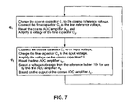
- FIGS. 6 and 7 show a flow chart for the timing diagram of FIG. 5 ;
- FIGS. 8 and 9 show the coarse and fine ADC's as amplifier arrays.
- FIG. 10 shows the circuit of FIG. 2 with FET transistors used as switches.
- FIG. 11 shows cascaded coarse and fine amplifier stages.
- This disclosure describes a subranging ADC that uses a two-phase clock timing method that permits the use of a T/H instead of a S/H, thus enabling a low-power, low-area implementation on a chip.
- the timing technique described herein can use a T/H, instead of a S/H, and does not require time-interleaved ADC's in order to realize high-speed operation.
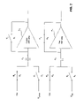
- FIG. 2 shows a single coarse amplifier A C and a single fine amplifier A F that illustrate the proposed timing method of the present invention.
- the coarse amplifier A C and the fine amplifier A F are implemented using auto-zero amplifiers. See, e.g., http://www.web-ee.com/primers/files/auto-zero_amps.pdf. for a general discussion of auto-zero amplifiers. (To the extent the overall block diagram of the architecture is the same as that in FIG. 1 , the same reference labels will be used herein.
- the coarse ADC 102 and the fine ADC 105 actually include an array of coarse amplifiers and an array of fine amplifiers. See, e.g., The Circuits and Filters Handbook , Wai-Kai Chen, ed., 1995, at 2099, for a discussion of subranging ADC's. See also FIGS. 8 and 9 , and discussion below.
- the coarse amplifier A c is connected to a capacitor C 1 , which in turn is connected to either the output of a track-and-hold 101 , or to V coarse from the reference ladder 104 .
- a two-phase clock including phases ⁇ 1 and ⁇ 2 , is used to control switches S 1 , S 2 and S 3 of the coarse amplifier A c .
- the switch S 1 is open.
- the coarse ADC amplifier A c is in a reset mode, and the capacitor C 1 is connected to the reference ladder tap V coarse .
- the switch S 5 is closed, the switches S 4 and S 6 are open, and the fine capacitor C 2 is connected to an appropriate tap of the reference ladder V fine .
- all of the switches as S 1 -S 6 are typically field effect transistor (FET) switches (see FIG. 10 , where the switches are S 1 -S 6 illustrated as FET devices).
- the switch S 3 may be referred to as a coarse ADC reset switch, and the switch S 6 may be referred to as a fine ADC reset switch.
- the switches S 3 and S 2 are closed, the amplifier A c is in a reset mode, and the left side of the capacitor C 1 is connected to a tap of the reference ladder (i.e., V coarse ).
- the switch S 1 is open when ⁇ 1 is on.
- the operation of the fine ADC amplifier A F may be thought of as an inverse of the operation of the amplifier A C .
- the clock phase ⁇ 2 when the clock phase ⁇ 2 is on, the left side of the capacitor C 2 is connected to the track-and-hold through switch S 4 , and the amplifier A F is in the reset mode, since the switch S 6 is closed, and the switch S 5 is open.
- a switch S 5 is closed to connect the capacitor C 2 to V fine , (a subrange from the reference ladder 104 ), the switches S 4 and S 6 are open, and the amplifier A F is in the amplify mode.
- the capacitors C 1 and C 2 are typically 50 to 200 femtofarads.
- the coarse amplifiers A C are reset to the reference ladder 104 , while the fine amplifiers A F amplify the previous sample.
- the coarse amplifiers A C amplify the next sample, while the fine amplifiers A F reset to the next sample.
- the fine ADC amplifier A F has a half cycle latency compared to the coarse ADC amplifier A C .
- one half of a clock cycle is available to do coarse quantization (and 1 ⁇ 2 cycle is available for fine quantization).
- the auto-zero amplifiers can be connected either to the T/H or to a reference voltage. An important difference between these two possibilities is that resetting all amplifiers to a reference voltage requires half a clock cycle less latency in comparison with resetting to the T/H output voltage.
- the coarse ADC amplifier A C has one half of a clock cycle to set switches in the switch matrix 103 , in order for the switch matrix 103 to pass the correct V fine reference ladder 104 output to the fine ADC 105 . While the amplifiers A C and A F require two phases to operate, the capacitors C 1 and C 2 subtract the V coarse from the track-and-hold output, or V fine from the track-and-hold output, respectively.
- the track-and-hold 101 only outputs the signal for half a period, and C 1 is charged early, before the track-and-hold 101 is ready.
- the amplifier A C immediately does the amplification.
- FIG. 2 shows only one coarse amplifier and one fine ADC amplifier A F , each can be part of an array of amplifiers in one embodiment of the invention.
- the amplifiers connect to the T/H during one half clock cycle, and to reference voltage taps (V coarse or V fine ) from the reference ladder 104 during a second half clock cycle.
- the amplifiers A C and A F are typically differential pair auto-zero amplifiers, with resistive load, preferably done in CMOS technology, e.g., NMOS or PMOS.
- CMOS technology e.g., NMOS or PMOS.
- the amplifiers A C and A F can be fabricated using bipolar technology.
- FIG. 3 shows how a two-phase non-overlapping clock can be converted to a three phase clock to better fine tune the ability of the coarse and fine amplifiers A C , A F and the comparators 107 , 108 settle to their final values.
- the phase ⁇ 2 can be split up into ⁇ 2 and ⁇ 2e , where ⁇ 2e represents an early falling edge of the clock phase ⁇ 2 .
- ⁇ 1 can be used to generate a phase ⁇ 1d — fine , a delayed ⁇ 1 phase of the clock used by the fine ADC 105 .
- the coarse ADC amplifier A C starts amplifying on the rising edge of ⁇ 2e , and stops amplifying on the falling edge of ⁇ 2e .
- the fine ADC amplifier A F is in a reset mode during that phase.
- the coarse amplifier A C begins resetting on the rising edge of ⁇ 1 , and stops resetting on the falling edge of ⁇ 1 .
- the comparators 107 of the coarse ADC 102 have from between the falling edge of ⁇ 2e through the rising edge of ⁇ 1d — fine to decide on whether they are latching 1 or 0 by comparing to a reference voltage from the reference ladder 104 .
- Each fine amplifier A F is actually a cascade of amplifiers, GA, GB, GC, GD, as discussed below, and which is particularly useful in a pipelined architecture.
- the first amplifier in the cascade, GA amplifies between the rising edge of ⁇ 1d — fine through the falling edge of ⁇ 1d — fine .
- FIG. 4 further illustrates the operation of the amplifiers of the present invention in a situation where the fine ADC 105 has 4 cascaded stages (typically with a gain of 4 ⁇ each), which are labeled GA, GB, GC and GD.
- the amplifier stage of the coarse ADC 102 is labeled GE
- the coarse ADC comparator 107 is labeled CC
- the fine ADC comparator 108 is labeled FC
- the encoder is labeled ENC.
- the gray portions of FIG. 4 illustrate a progression of one sample's quantization down the amplifier cascade.
- the track-and-hold 101 is connected to the coarse ADC amplifier A c , during phase ⁇ 2 .
- the coarse comparator 107 (CC) is reset during ⁇ 2 .
- the fine ADC amplifier A F stage GA is also reset.
- the first stage GA of the fine ADC 105 amplifies, while the second stage GB resets.
- the process continues, as the signal moves in a pipelined manner down from GA to GB to GC to GD to the fine comparator 108 (FC), and ultimately to the encoder 106 .
- the next quantization is directly behind the quantization just performed, moving from left to right in the figure, and offset by one clock cycle from the measurement illustrated in gray in FIG. 4 .
- FIGS. 5 and 6 illustrates the operation of the coarse/fine ADC's 102 / 105 in greater detail, showing the relationship between the clock phases of the three phase clock discussed above, and the operation of the various components shown in FIG. 2 .
- the coarse capacitor C 1 is connected to the reference ladder 104 voltage V ref (i.e., V coarse ) on the rising edge of the clock phase ⁇ 1 .
- V ref i.e., V coarse
- the coarse amplifier 102 is also reset on the rising edge of ⁇ 1 , with the switch S 3 being closed until the falling edge of ⁇ 1 .
- the switch S 2 is kept closed until the falling edge of ⁇ 1d (the delayed edge of ⁇ 1 ).
- the coarse capacitor C 1 is connected to the track-and-hold 101 , and the coarse amplifier A C begins amplifying the signal.
- the coarse comparator 107 (CC) is reset on the rising edge of ⁇ 2
- the fine capacitor C 2 is connected to the track-and-hold voltage.
- the fine amplifier A F is also reset on the rising edge of ⁇ 2 .
- the coarse capacitor C 1 is connected to the track-and-hold 101 until the falling edge of ⁇ 2d (for delayed ⁇ 2 ), the coarse comparator 107 (CC) begins latching at the falling edge of ⁇ 2e (for early ⁇ 2 ) and the fine amplifier A F continues to be reset until the falling edge of ⁇ 2 .
- the fine capacitor C 2 is connected to the T/H through the delayed falling edge of ⁇ 2 ( ⁇ 2d ).
- the coarse comparator 107 (CC) is assumed to have latched at the rising edge of ⁇ 1d — fine , while the fine capacitor C 2 is connected to the reference voltage and fine amplifier A F begins to amplify, also on the rising edge of ⁇ 1d — fine , The connection of the capacitor C 2 to the reference ladder 104 lasts until the falling edge of ⁇ 1d , and the fine amplifier A F stops amplifying on the falling edge of ⁇ 1d .
- the digital output of the coarse ADC tells the fine ADC 105 which subrange from the reference ladder voltage V ref (i.e., V fine ) the switch matrix 103 should pass through to the fine ADC 105 .
- Each amplifier amplifies only if there is a valid signal period.
- the hold phase is the middle 1 ⁇ 3 phase of FIG. 5 —both the coarse amplifier A C and the fine amplifier A F are looking at the signal.
- an array of 30 coarse amplifiers and an array of 30 coarse comparators are used to get 31 subranges.
- the switch matrix 103 therefore connects to one out of 31 subranges.
- the embodiment includes an array of 19 A-stage amplifiers, an array of 33 B-stage amplifiers, an array of 65 C-stage amplifiers and an array of 65 D-stage amplifiers, as well as an array of 65 fine comparators.
- the fine ADC 105 of the present invention is illustrated in array form in FIG. 9 , showing a plurality of amplifiers A F0 -A Fn , connected to a plurality of input capacitors C F0 , and through the input capacitors C Fn to a plurality of fine taps from the reference ladder 104 , taps V fine,0 to V fine,n .
- n 18.
- the auto-zero amplifiers A C0 -A Cm and A F0 -A Fn are shown as single ended in FIGS. 8 and 9 , in actual application they are preferably differential amplifiers.
- An “11 bit” output is actually converted to a 10-bit output, to compensate for conversion errors of the coarse ADC.
- a single ADC can be run at F sample , since there is delay of the latency of the fine ADC 105 by one half of a clock cycle.
- the switches S 1 , S 2 and S 4 shown on the left-side of the sampling capacitors C 1 , C 2 in FIG. 2 can use slightly delayed clocks ⁇ 1d and ⁇ 2d .
- the coarse comparators 107 use an earlier clock signal ⁇ 1e , to give them somewhat more time to compare their input signal, thus improving their bit-error-rate.
- the switch S 5 connecting the fine amplifiers A F to the reference ladder 104 use a delayed clock, ⁇ 1dfine , for the same reason. Basically, this implements a three-phase clock to operate the coarse ADC 102 .
- the proposed timing can be applied to all subranging ADC's to improve the required power and area.
Abstract
Description
Claims (27)
Priority Applications (1)
| Application Number | Priority Date | Filing Date | Title |
|---|---|---|---|
| US10/625,702 US7324038B2 (en) | 2002-05-24 | 2003-07-24 | Subranging analog to digital converter with multi-phase clock timing |
Applications Claiming Priority (4)
| Application Number | Priority Date | Filing Date | Title |
|---|---|---|---|
| US10/153,709 US6628224B1 (en) | 2002-05-24 | 2002-05-24 | Distributed averaging analog to digital converter topology |
| US10/158,773 US6583747B1 (en) | 2002-05-24 | 2002-05-31 | Subranging analog to digital converter with multi-phase clock timing |
| US10/359,201 US6653966B1 (en) | 2002-05-24 | 2003-02-06 | Subranging analog to digital converter with multi-phase clock timing |
| US10/625,702 US7324038B2 (en) | 2002-05-24 | 2003-07-24 | Subranging analog to digital converter with multi-phase clock timing |
Related Parent Applications (1)
| Application Number | Title | Priority Date | Filing Date |
|---|---|---|---|
| US10/359,201 Continuation US6653966B1 (en) | 2002-05-24 | 2003-02-06 | Subranging analog to digital converter with multi-phase clock timing |
Publications (2)
| Publication Number | Publication Date |
|---|---|
| US20040155807A1 US20040155807A1 (en) | 2004-08-12 |
| US7324038B2 true US7324038B2 (en) | 2008-01-29 |
Family
ID=29552747
Family Applications (3)
| Application Number | Title | Priority Date | Filing Date |
|---|---|---|---|
| US10/158,773 Expired - Fee Related US6583747B1 (en) | 2002-05-24 | 2002-05-31 | Subranging analog to digital converter with multi-phase clock timing |
| US10/359,201 Expired - Lifetime US6653966B1 (en) | 2002-05-24 | 2003-02-06 | Subranging analog to digital converter with multi-phase clock timing |
| US10/625,702 Expired - Lifetime US7324038B2 (en) | 2002-05-24 | 2003-07-24 | Subranging analog to digital converter with multi-phase clock timing |
Family Applications Before (2)
| Application Number | Title | Priority Date | Filing Date |
|---|---|---|---|
| US10/158,773 Expired - Fee Related US6583747B1 (en) | 2002-05-24 | 2002-05-31 | Subranging analog to digital converter with multi-phase clock timing |
| US10/359,201 Expired - Lifetime US6653966B1 (en) | 2002-05-24 | 2003-02-06 | Subranging analog to digital converter with multi-phase clock timing |
Country Status (1)
| Country | Link |
|---|---|
| US (3) | US6583747B1 (en) |
Cited By (13)
| Publication number | Priority date | Publication date | Assignee | Title |
|---|---|---|---|---|
| US20080048896A1 (en) * | 2006-08-25 | 2008-02-28 | Broadcom Corporation | Gain control for interleaved analog-to-digital conversion for electronic dispersion compensation |
| US20080049825A1 (en) * | 2006-08-25 | 2008-02-28 | Broadcom Corporation | Equalizer with reorder |
| US20080048897A1 (en) * | 2006-08-25 | 2008-02-28 | Broadcom Corporation | Phase control for interleaved analog-to-digital conversion for electronic dispersion compensation |
| US20080069198A1 (en) * | 2006-08-25 | 2008-03-20 | Broadcom Corporation | Sequence decision feedback equalizer |
| US20080187082A1 (en) * | 2006-08-25 | 2008-08-07 | Broadcom Corporation | Electronic dispersion compensation utilizing interleaved architecture and channel identification for assisting timing recovery |
| US20080238542A1 (en) * | 2006-08-25 | 2008-10-02 | Namik Kocaman | Variable gain amplifier and method for achieving variable gain amplification with high bandwidth and linearity |
| US20090174585A1 (en) * | 2007-08-06 | 2009-07-09 | Swain Allan L | System and method for converting analog values into digital form |
| US7961781B2 (en) | 2006-08-25 | 2011-06-14 | Broadcom Corporation | Electronic dispersion compensation utilizing interleaved architecture and channel identification for assisting timing recovery |
| US20120268300A1 (en) * | 2011-04-20 | 2012-10-25 | Sony Corporation | Analog-to-digital converter and signal processing system |
| US8300685B2 (en) | 2006-08-25 | 2012-10-30 | Broadcom Corporation | Non-linear decision feedback equalizer |
| US9571043B1 (en) | 2015-10-01 | 2017-02-14 | Avago Technologies General Ip (Singapore) Pte. Ltd. | Auxiliary control of system offsets |
| US10461763B2 (en) * | 2017-01-31 | 2019-10-29 | Huawei Technologies Co., Ltd. | Double data rate time interpolating quantizer with reduced kickback noise |
| US20190356327A1 (en) * | 2017-01-31 | 2019-11-21 | Huawei Technologies Co., Ltd. | Double Data Rate Interpolating Analog to Digital Converter |
Families Citing this family (38)
| Publication number | Priority date | Publication date | Assignee | Title |
|---|---|---|---|---|
| US6628224B1 (en) * | 2002-05-24 | 2003-09-30 | Broadcom Corporation | Distributed averaging analog to digital converter topology |
| US6697005B2 (en) * | 2002-05-24 | 2004-02-24 | Broadcom Corporation | Analog to digital converter with interpolation of reference ladder |
| US6583747B1 (en) * | 2002-05-24 | 2003-06-24 | Broadcom Corporation | Subranging analog to digital converter with multi-phase clock timing |
| US7271755B2 (en) * | 2002-05-24 | 2007-09-18 | Broadcom Corporation | Resistor ladder interpolation for PGA and DAC |
| US7190298B2 (en) | 2002-05-24 | 2007-03-13 | Broadcom Corporation | Resistor ladder interpolation for subranging ADC |
| EP1588492B1 (en) * | 2003-01-17 | 2007-03-28 | Koninklijke Philips Electronics N.V. | An analog-to-digital conversion arrangement, a method for analog-to-digital conversion and a signal processing system, in which the conversion arrangement is applied |
| US6999019B2 (en) * | 2004-04-08 | 2006-02-14 | The Boeing Company | Subranging analog-to-digital converter with integrating sample-and-hold |
| US6967603B1 (en) * | 2004-07-19 | 2005-11-22 | Realtek Semiconductor Corp. | ADC background calibration timing |
| US7015852B1 (en) * | 2004-11-30 | 2006-03-21 | Freescale Semiconductor, Inc. | Cyclic analog-to-digital converter |
| US7292170B2 (en) * | 2005-06-13 | 2007-11-06 | Texas Instruments Incorporated | System and method for improved time-interleaved analog-to-digital converter arrays |
| JP4864740B2 (en) * | 2007-01-25 | 2012-02-01 | 株式会社東芝 | Analog to digital converter |
| US7443332B2 (en) * | 2007-03-26 | 2008-10-28 | National Instruments Corporation | Time continuous pipeline analog-to-digital converter |
| US7567197B2 (en) * | 2007-09-17 | 2009-07-28 | Samsung Electronics Co., Ltd. | Cascade comparator and control method thereof |
| US7626531B2 (en) * | 2008-02-01 | 2009-12-01 | Agere Systems Inc. | Systems and methods for analog to digital conversion |
| US7573415B1 (en) * | 2008-02-01 | 2009-08-11 | Agere Systems Inc. | Area and power efficient analog to digital converter and methods for using such |
| EP2198520A4 (en) | 2008-06-06 | 2012-11-21 | Lsi Corp | Systems and methods for latch based analog to digital conversion |
| US8121186B2 (en) | 2008-06-06 | 2012-02-21 | Lsi Corporation | Systems and methods for speculative signal equalization |
| JP5244233B2 (en) | 2008-06-06 | 2013-07-24 | エルエスアイ コーポレーション | System and method for synchronous timing reset analog-to-digital conversion |
| WO2010004455A2 (en) * | 2008-06-16 | 2010-01-14 | Nxp B.V. | A switched-capacitor pipeline adc stage |
| US8188901B1 (en) * | 2008-08-15 | 2012-05-29 | Hypres, Inc. | Superconductor analog to digital converter |
| US8049652B2 (en) | 2009-01-20 | 2011-11-01 | Marvell International Ltd. | Reference pre-charging for two-step subranging ADC architecture |
| US8574960B2 (en) | 2010-02-03 | 2013-11-05 | Stats Chippac, Ltd. | Semiconductor device and method of forming cavity adjacent to sensitive region of semiconductor die using wafer-level underfill material |
| US8339302B2 (en) * | 2010-07-29 | 2012-12-25 | Freescale Semiconductor, Inc. | Analog-to-digital converter having a comparator for a multi-stage sampling circuit and method therefor |
| US8248290B2 (en) * | 2010-09-13 | 2012-08-21 | Texas Instruments Incorporated | Multiplexed amplifier with reduced glitching |
| US8193961B2 (en) | 2010-09-23 | 2012-06-05 | Lsi Corporation | Systems and methods for enhancing analog to digital conversion resolution |
| US8638252B2 (en) * | 2011-11-30 | 2014-01-28 | Tensorcom, Inc | Low power high speed A/D converter |
| TWI462487B (en) * | 2011-12-23 | 2014-11-21 | Ind Tech Res Inst | Analog to digital converting apparatus and method thereof |
| US8957801B2 (en) * | 2012-06-11 | 2015-02-17 | Dan Raphaeli | Method and system for flash type analog to digital converter |
| US8730073B1 (en) * | 2012-12-18 | 2014-05-20 | Broadcom Corporation | Pipelined analog-to-digital converter with dedicated clock cycle for quantization |
| US9258005B2 (en) * | 2014-06-30 | 2016-02-09 | Infineon Technologies Ag | Sensor system using multiple modes for analog to digital conversion |
| US9455734B2 (en) * | 2014-06-30 | 2016-09-27 | Infineon Technologies Ag | Sensor system using multiple modes for analog to digital conversion |
| US9799349B2 (en) * | 2015-04-24 | 2017-10-24 | Cirrus Logic, Inc. | Analog-to-digital converter (ADC) dynamic range enhancement for voice-activated systems |
| US10250275B2 (en) * | 2015-07-02 | 2019-04-02 | Hewlett Packard Enterprises Development LP | Digital voltage sampling |
| US9602120B1 (en) | 2016-04-04 | 2017-03-21 | International Business Machines Corporation | Analog to digital converter with digital reference voltage signal |
| TWI660592B (en) | 2018-07-20 | 2019-05-21 | 瑞昱半導體股份有限公司 | Analog-to-digital converter |
| US10438677B1 (en) | 2018-11-20 | 2019-10-08 | Nxp B.V. | Modular sample-and-hold circuit |
| US10630304B1 (en) | 2019-04-01 | 2020-04-21 | Nxp B.V. | Sub-ranging analog-to-digital converter |
| US11233521B2 (en) * | 2019-07-16 | 2022-01-25 | Uti Limited Partnership | Sub-ranging analog to digital converter |
Citations (13)
| Publication number | Priority date | Publication date | Assignee | Title |
|---|---|---|---|---|
| US3697978A (en) | 1970-10-19 | 1972-10-10 | Singer Co | Analog-to-digital converter |
| US5191336A (en) | 1991-08-29 | 1993-03-02 | Hewlett-Packard Company | Digital time interpolation system |
| US5302869A (en) * | 1991-10-03 | 1994-04-12 | Mitsubishi Denki Kabushiki Kaisha | Voltage comparator and subranging A/D converter including such voltage comparator |
| US5973632A (en) | 1998-03-03 | 1999-10-26 | Powerchip Semiconductor Corp. | Sub-range flash analog-to-digital converter |
| US6104332A (en) * | 1998-09-30 | 2000-08-15 | National Semiconductor Corporation | Absolute value circuit and method |
| US6169502B1 (en) | 1998-05-08 | 2001-01-02 | Cirrus Logic, Inc. | Pipelined analog-to-digital converter (ADC) systems, methods, and computer program products |
| US6259745B1 (en) | 1998-10-30 | 2001-07-10 | Broadcom Corporation | Integrated Gigabit Ethernet transmitter architecture |
| US6489913B1 (en) | 2001-09-24 | 2002-12-03 | Tektronix, Inc. | Sub-ranging analog-to-digital converter using a sigma delta converter |
| US6583747B1 (en) * | 2002-05-24 | 2003-06-24 | Broadcom Corporation | Subranging analog to digital converter with multi-phase clock timing |
| US6674389B2 (en) * | 2001-02-09 | 2004-01-06 | Broadcom Corporation | Capacitive folding circuit for use in a folding/interpolating analog-to-digital converter |
| US6999019B2 (en) * | 2004-04-08 | 2006-02-14 | The Boeing Company | Subranging analog-to-digital converter with integrating sample-and-hold |
| US7102559B2 (en) * | 2003-01-17 | 2006-09-05 | Koninklijke Philips Electronics, N.V. | Analog-to-digital converter having interleaved coarse sections coupled to a single fine section |
| US7256725B2 (en) * | 2002-05-24 | 2007-08-14 | Broadcom Corporation | Resistor ladder interpolation for subranging ADC |
-
2002
- 2002-05-31 US US10/158,773 patent/US6583747B1/en not_active Expired - Fee Related
-
2003
- 2003-02-06 US US10/359,201 patent/US6653966B1/en not_active Expired - Lifetime
- 2003-07-24 US US10/625,702 patent/US7324038B2/en not_active Expired - Lifetime
Patent Citations (14)
| Publication number | Priority date | Publication date | Assignee | Title |
|---|---|---|---|---|
| US3697978A (en) | 1970-10-19 | 1972-10-10 | Singer Co | Analog-to-digital converter |
| US5191336A (en) | 1991-08-29 | 1993-03-02 | Hewlett-Packard Company | Digital time interpolation system |
| US5302869A (en) * | 1991-10-03 | 1994-04-12 | Mitsubishi Denki Kabushiki Kaisha | Voltage comparator and subranging A/D converter including such voltage comparator |
| US5973632A (en) | 1998-03-03 | 1999-10-26 | Powerchip Semiconductor Corp. | Sub-range flash analog-to-digital converter |
| US6169502B1 (en) | 1998-05-08 | 2001-01-02 | Cirrus Logic, Inc. | Pipelined analog-to-digital converter (ADC) systems, methods, and computer program products |
| US6104332A (en) * | 1998-09-30 | 2000-08-15 | National Semiconductor Corporation | Absolute value circuit and method |
| US6259745B1 (en) | 1998-10-30 | 2001-07-10 | Broadcom Corporation | Integrated Gigabit Ethernet transmitter architecture |
| US6674389B2 (en) * | 2001-02-09 | 2004-01-06 | Broadcom Corporation | Capacitive folding circuit for use in a folding/interpolating analog-to-digital converter |
| US6489913B1 (en) | 2001-09-24 | 2002-12-03 | Tektronix, Inc. | Sub-ranging analog-to-digital converter using a sigma delta converter |
| US6583747B1 (en) * | 2002-05-24 | 2003-06-24 | Broadcom Corporation | Subranging analog to digital converter with multi-phase clock timing |
| US6653966B1 (en) * | 2002-05-24 | 2003-11-25 | Broadcom Corporation | Subranging analog to digital converter with multi-phase clock timing |
| US7256725B2 (en) * | 2002-05-24 | 2007-08-14 | Broadcom Corporation | Resistor ladder interpolation for subranging ADC |
| US7102559B2 (en) * | 2003-01-17 | 2006-09-05 | Koninklijke Philips Electronics, N.V. | Analog-to-digital converter having interleaved coarse sections coupled to a single fine section |
| US6999019B2 (en) * | 2004-04-08 | 2006-02-14 | The Boeing Company | Subranging analog-to-digital converter with integrating sample-and-hold |
Non-Patent Citations (32)
| Title |
|---|
| Abo, A.M. and Gray, P.R., "A 1.5-V, 10-bit, 14.3-MS/s CMOS Pipeline Analog-to-Digital Converter," IEEE Journal of Solid-State Circuits, IEEE, vol. 34, No. 5, May 1999, pp. 599-606. |
| Brandt, B.P. and Lutsky, J., "A 75-mW, 10-b, 20-MSPS CMOS Subranging ADC with 9.5 Effective Bits at Nyquist," IEEE Journal of Solid-State Circuits, IEEE, vol. 34, No. 12, Dec. 1999, pp. 1788-1795. |
| Bult, Klaas and Buchwald, Aaron, "An Embedded 240-mW 10-b 50-MS/s CMOS ADC in 1-mm<SUP>2</SUP>," IEEE Journal of Solid-State Circuits, IEEE, vol. 32, No. 12, Dec. 1997, pp. 1887-1895. |
| Cho, T.B. and Gray, P.R., "A 10 b, 20 Msample/s, 35 mW Pipeline A/D Converter," IEEE Journal of Solid-State Circuits, IEEE, vol. 30, No. 3, Mar. 1995, pp. 166-172. |
| Choe, M-J. et al., "A 13-b 40-Msamples/s CMOS Pipelined Folding ADC with Background Offset Trimming," IEEE Journal of Solid-State Circuits, IEEE, vol. 35, No. 12, Dec. 2000, pp. 1781-1790. |
| Choi, M. and Abidi, A., "A 6-b 1.3-Gsample/s A/D Converter in 0.35-mum CMOS," IEEE Journal of Solid-State Circuits, IEEE, vol. 36, No. 12, Dec. 2001, pp. 1847-1858. |
| Dingwall et al., IEEE Journal of Solid-State Circuits, vol. SC-20, No. 6, "An 8-MHz CMOS Subranging 8-Bit A/D Converter", Dec. 1985, pp. 1138-1143. |
| Flynn, M. and Sheahan, B., "A 400-Msample/s, 6-b CMOS Folding and Interpolating ADC," IEEE Journal of Solid-State Circuits, IEEE, vol. 33, No. 12, Dec. 1998, pp. 1932-1938. |
| Geelen, G., "A 6b 1.1GSample/s CMOS A/D Converter," IEEE International Solid-State Circuits Conference, IEEE, 2001, pp. 128-129 and 438, no month/date. |
| Hoogzaad, G. and Roovers, R., "A 65-mW, 10-bit, 40-Msample/s BiCMOS Nyquist ADC in 0.8 mm<SUP>2</SUP>," IEEE Journal of Solid-State Circuits, IEEE, vol. 34, No. 12, Dec. 1999, pp. 1796-1802. |
| Hosotani, S. et al., "An 8-bit 20-MS/s CMOS A/D Converter with 50-mW Power Consumption," IEEE Journal of Solid-State Circuits, IEEE, vol. 25, No. 1, Feb. 1990, pp. 167-172. |
| Ingino, J.M. and Wooley, B.A., "A Continuously Calibrated 12-b, 10-MS/s, 3.3-V A/D Converter," IEEE Journal of Solid-State Circuits, IEEE, vol. 33, No. 12, Dec. 1998, pp. 1920-1931. |
| Ito, M. et al., "A 10 bit 20 MS/s 3 V Supply CMOS A/D Converter," IEEE Journal of Solid-State Circuits, IEEE, vol. 29, No. 12, Dec. 1994, pp. 1531-1536. |
| Kattman, K. and Barrow, J., "A Technique for Reducing Differential Non-Linearity Errors in Flash A/D Converters," IEEE International Solid-State Conference, IEEE, 1991, pp. 170-171, no month/date. |
| Kusumoto, K. et al., "A 10-b 20-MHz 30-mW Pipelined Interpolating CMOS ADC," IEEE Journal of Solid-State Circuits, IEEE, vol. 28, No. 12, Dec. 1993, pp. 1200-1206. |
| Lewis, S. et al., "A 10-b 20-Msample/s Analog-to-Digital Converter," IEEE Journal of Solid-State Circuits, IEEE, vol. 27, No. 3, Mar. 1992, pp. 351-358. |
| Mehr, I. and Singer, L., "A 55-mW, 10-bit, 40-Msample/s Nyquist-Rate CMOS ADC," IEEE Journal of Solid-State Circuits, IEEE, vol. 35, No. 3, Mar. 2000, pp. 318-325. |
| Miyazaki et al., ISSCC 2002/Session 10/High-Speed ADCs/10.5, "A 16mW 30 MSample/s 10b Pipelined A/D Converter using a Pseudo-Differential Architecture", Feb. 5, 2002, 3 pgs. |
| Nagaraj, K. et al., "A Dual-Mode 700-Msamples/s 6-bit 200-Msample/s 7-bit A/D Converter in a 0.25-mum Digital CMOS," IEEE Journal of Solid-State Circuits, IEEE, vol. 35, No. 12, Dec. 2000, pp. 1760-1768. |
| Nagaraj, K. et al., "Efficient 6-Bit A/D Converter Using a 1-Bit Folding Front End," IEEE Journal of Solid-State Circuits, IEEE, vol. 34, No. 8, Aug. 1999, pp. 1056-1062. |
| Nauta, B. and Venes, A., "A 70-MS/s 110-mW 8-b CMOS Folding and Interpolating A/D Converter," IEEE Journal of Solid-State Circuits, IEEE, vol. 30, No. 12, Dec. 1995, pp. 1302-1308. |
| Pan, H. et al., "A 3.3-V 12-b 50-MS/s A/D Converter in 0.6-mum CMOS with over 80-dB SFDR," IEEE Journal of Solid-State Circuits, IEEE, vol. 35, No. 12, Dec. 2000, pp. 1769-1780. |
| Song, W-C. et al., "A 10-b 20-Msample/s Low-Power CMOS ADC," IEEE Journal of Solid-State Circuits, IEEE, vol. 30, No. 5, May 1995, pp. 514-521. |
| Sumanen, L. et al., "A 10-bit 200-MS/s CMOS Parallel Pipeline A/D Converter," IEEE Journal of Solid-State Circuits, IEEE, vol. 36, No. 7, Jul. 2001, pp. 1048-1055. |
| Sushihara et al., ISSCC 2002/Session 10/High-Speed ADCs/10.3, "A 7b 450 MSample/s 50mW CMOS ADC in 0.3 mm<SUP>2</SUP>", Feb. 5, 2002, 3 pgs. |
| Taft, R.C. and Tursi, M.R., "A 100-MS/s 8-b CMOS Subranging ADC with Sustained Parametric Performance from 3.8 V Down to 2.2 V," IEEE Journal of Solid-State Circuits, IEEE, vol. 36, No. 3, Mar. 2001, pp. 331-338. |
| van der Ploeg, H. and Remmers, R., "A 3.3-V, 10-b 25-Msample/s Two-Step ADC in 0.35-mum CMOS," IEEE Journal of Solid-State Circuits, IEEE, vol. 34, No. 12, Dec. 1999, pp. 1803-1811. |
| van der Ploeg, H. et al., "A 2.5-V 12-b 54-Msample/s 0.25-mum CMOS ADC in 1-mm<SUP>2 </SUP>With Mixed-Signal Chopping and Calibration," IEEE Journal of Solid-State Circuits, IEEE, vol. 36, No. 12, Dec. 2001, pp. 1859-1867. |
| Vorenkamp, P. and Roovers, R., "A 12-b, 60-Msample/s Cascaded Folding and Interpolating ADC," IEEE Journal of Solid-State Circuits, IEEE, vol. 32, No. 12, Dec. 1997, pp. 1876-1886. |
| Wang, Y-T. and Razavi, B., "An 8-bit 150-MHz CMOS A/D Converter," IEEE Journal of Solid-State Circuits, IEEE, vol. 35, No. 3, Mar. 2000, pp. 308-317. |
| Yotsuyanagi, M. et al., "A 2 V, 10 b, 20 Msample/s, Mixed-Mode Subranging CMOS A/D Converter," IEEE Journal of Solid-State Circuits, IEEE, vol. 30, No. 12, Dec. 1995, pp. 1533-1537. |
| Yu, P.C. and Lee, H-S., "A 2.5-V, 12-b, 5-Msample/s Pipelined CMOS ADC," IEEE Journal of Solid-State Circuits, IEEE, vol. 31, No. 12, Dec. 1996, pp. 1854-1861. |
Cited By (21)
| Publication number | Priority date | Publication date | Assignee | Title |
|---|---|---|---|---|
| US7560986B2 (en) | 2006-08-25 | 2009-07-14 | Broadcom Corporation | Variable gain amplifier and method for achieving variable gain amplification with high bandwidth and linearity |
| US20080187082A1 (en) * | 2006-08-25 | 2008-08-07 | Broadcom Corporation | Electronic dispersion compensation utilizing interleaved architecture and channel identification for assisting timing recovery |
| US20080048896A1 (en) * | 2006-08-25 | 2008-02-28 | Broadcom Corporation | Gain control for interleaved analog-to-digital conversion for electronic dispersion compensation |
| US7830987B2 (en) | 2006-08-25 | 2010-11-09 | Broadcom Corporation | Electronic dispersion compensation utilizing interleaved architecture and channel identification for assisting timing recovery |
| US7755426B2 (en) | 2006-08-25 | 2010-07-13 | Broadcom Corporation | Variable gain amplifier and method for achieving variable gain amplification with high bandwidth and linearity |
| US20080238542A1 (en) * | 2006-08-25 | 2008-10-02 | Namik Kocaman | Variable gain amplifier and method for achieving variable gain amplification with high bandwidth and linearity |
| US20080258814A1 (en) * | 2006-08-25 | 2008-10-23 | Broadcom Corporation | Variable gain amplifier and method for achieving variable gain amplification with high bandwidth and linearity |
| US7525462B2 (en) | 2006-08-25 | 2009-04-28 | Broadcom Corporation | Gain control for interleaved analog-to-digital conversion for electronic dispersion compensation |
| US7525470B2 (en) * | 2006-08-25 | 2009-04-28 | Broadcom Corporation | Phase control for interleaved analog-to-digital conversion for electronic dispersion compensation |
| US8300685B2 (en) | 2006-08-25 | 2012-10-30 | Broadcom Corporation | Non-linear decision feedback equalizer |
| US20080048897A1 (en) * | 2006-08-25 | 2008-02-28 | Broadcom Corporation | Phase control for interleaved analog-to-digital conversion for electronic dispersion compensation |
| US20080049825A1 (en) * | 2006-08-25 | 2008-02-28 | Broadcom Corporation | Equalizer with reorder |
| US20080069198A1 (en) * | 2006-08-25 | 2008-03-20 | Broadcom Corporation | Sequence decision feedback equalizer |
| US7961781B2 (en) | 2006-08-25 | 2011-06-14 | Broadcom Corporation | Electronic dispersion compensation utilizing interleaved architecture and channel identification for assisting timing recovery |
| US20090174585A1 (en) * | 2007-08-06 | 2009-07-09 | Swain Allan L | System and method for converting analog values into digital form |
| US20120268300A1 (en) * | 2011-04-20 | 2012-10-25 | Sony Corporation | Analog-to-digital converter and signal processing system |
| US8487801B2 (en) * | 2011-04-20 | 2013-07-16 | Sony Corporation | Analog-to-digital converter and signal processing system |
| US9571043B1 (en) | 2015-10-01 | 2017-02-14 | Avago Technologies General Ip (Singapore) Pte. Ltd. | Auxiliary control of system offsets |
| US10461763B2 (en) * | 2017-01-31 | 2019-10-29 | Huawei Technologies Co., Ltd. | Double data rate time interpolating quantizer with reduced kickback noise |
| US20190356327A1 (en) * | 2017-01-31 | 2019-11-21 | Huawei Technologies Co., Ltd. | Double Data Rate Interpolating Analog to Digital Converter |
| US10771084B2 (en) * | 2017-01-31 | 2020-09-08 | Huawei Technologies Co., Ltd. | Double data rate interpolating analog to digital converter |
Also Published As
| Publication number | Publication date |
|---|---|
| US6653966B1 (en) | 2003-11-25 |
| US6583747B1 (en) | 2003-06-24 |
| US20030218556A1 (en) | 2003-11-27 |
| US20040155807A1 (en) | 2004-08-12 |
Similar Documents
| Publication | Publication Date | Title |
|---|---|---|
| US7324038B2 (en) | Subranging analog to digital converter with multi-phase clock timing | |
| US7215274B2 (en) | Reference voltage pre-charge in a multi-step sub-ranging analog-to-digital converter | |
| US5710563A (en) | Pipeline analog to digital converter architecture with reduced mismatch error | |
| US7397409B2 (en) | Multi-bit pipeline analog-to-digital converter having shared amplifier structure | |
| EP1917719B1 (en) | Switched-capacitor circuit with scaled reference voltage | |
| US7187318B1 (en) | Pipeline ADC using multiplying DAC and analog delay circuits | |
| US6366230B1 (en) | Pipelined analog-to-digital converter | |
| US20090184857A1 (en) | A/d converting apparatus | |
| US8902093B1 (en) | Parallel analog to digital converter architecture with charge redistribution and method thereof | |
| US7224306B2 (en) | Analog-to-digital converter in which settling time of amplifier circuit is reduced | |
| US7852254B1 (en) | 1-bit cell circuit used in a pipelined analog to digital converter | |
| US6956519B1 (en) | Switched capacitor circuit of a pipeline analog to digital converter and a method for operating the switched capacitor circuit | |
| US6229472B1 (en) | A/D converter | |
| US6285309B1 (en) | Nested pipelined analog-to-digital converter | |
| US7791523B2 (en) | Two-step sub-ranging analog-to-digital converter and method for performing two-step sub-ranging in an analog-to-digital converter | |
| KR101287097B1 (en) | Four-channel pipelined sar adc to minimize mismatches between channels | |
| US7002507B2 (en) | Pipelined and cyclic analog-to-digital converters | |
| US7102559B2 (en) | Analog-to-digital converter having interleaved coarse sections coupled to a single fine section | |
| EP4285488A1 (en) | Lookup-table-based analog-to-digital converter | |
| US8299952B1 (en) | Switched-capacitor circuit and pipelined analog-to-digital converter | |
| KR100294787B1 (en) | Sub-ranging analog-to-digital converter with open-loop differential amplifiers | |
| US20090289821A1 (en) | Pipeline analog-to-digital converter having operational amplifier shared by sample and hold circuit and leading multiplying digital-to-analog converter | |
| US6859158B2 (en) | Analog-digital conversion circuit | |
| US8400343B1 (en) | Pipeline analog to digital converter with split-path level shifting technique | |
| US6232907B1 (en) | Polarity shifting flash A/D converter and method |
Legal Events
| Date | Code | Title | Description |
|---|---|---|---|
| AS | Assignment |
Owner name: BROADCOM CORPORATION, CALIFORNIA Free format text: ASSIGNMENT OF ASSIGNORS INTEREST;ASSIGNORS:VAN DER GOES, FRANCISCUS MARIA LEONARDUS;MULDER, JAN;WARD, CHRISTOPHER MICAHEL;AND OTHERS;REEL/FRAME:017928/0897;SIGNING DATES FROM 20040929 TO 20041005 |
|
| STCF | Information on status: patent grant |
Free format text: PATENTED CASE |
|
| CC | Certificate of correction | ||
| FPAY | Fee payment |
Year of fee payment: 4 |
|
| FPAY | Fee payment |
Year of fee payment: 8 |
|
| AS | Assignment |
Owner name: BANK OF AMERICA, N.A., AS COLLATERAL AGENT, NORTH CAROLINA Free format text: PATENT SECURITY AGREEMENT;ASSIGNOR:BROADCOM CORPORATION;REEL/FRAME:037806/0001 Effective date: 20160201 Owner name: BANK OF AMERICA, N.A., AS COLLATERAL AGENT, NORTH Free format text: PATENT SECURITY AGREEMENT;ASSIGNOR:BROADCOM CORPORATION;REEL/FRAME:037806/0001 Effective date: 20160201 |
|
| AS | Assignment |
Owner name: AVAGO TECHNOLOGIES GENERAL IP (SINGAPORE) PTE. LTD., SINGAPORE Free format text: ASSIGNMENT OF ASSIGNORS INTEREST;ASSIGNOR:BROADCOM CORPORATION;REEL/FRAME:041706/0001 Effective date: 20170120 Owner name: AVAGO TECHNOLOGIES GENERAL IP (SINGAPORE) PTE. LTD Free format text: ASSIGNMENT OF ASSIGNORS INTEREST;ASSIGNOR:BROADCOM CORPORATION;REEL/FRAME:041706/0001 Effective date: 20170120 |
|
| AS | Assignment |
Owner name: BROADCOM CORPORATION, CALIFORNIA Free format text: TERMINATION AND RELEASE OF SECURITY INTEREST IN PATENTS;ASSIGNOR:BANK OF AMERICA, N.A., AS COLLATERAL AGENT;REEL/FRAME:041712/0001 Effective date: 20170119 |
|
| AS | Assignment |
Owner name: AVAGO TECHNOLOGIES INTERNATIONAL SALES PTE. LIMITE Free format text: MERGER;ASSIGNOR:AVAGO TECHNOLOGIES GENERAL IP (SINGAPORE) PTE. LTD.;REEL/FRAME:047195/0658 Effective date: 20180509 |
|
| AS | Assignment |
Owner name: AVAGO TECHNOLOGIES INTERNATIONAL SALES PTE. LIMITE Free format text: CORRECTIVE ASSIGNMENT TO CORRECT THE EFFECTIVE DATE OF MERGER PREVIOUSLY RECORDED ON REEL 047195 FRAME 0658. ASSIGNOR(S) HEREBY CONFIRMS THE THE EFFECTIVE DATE IS 09/05/2018;ASSIGNOR:AVAGO TECHNOLOGIES GENERAL IP (SINGAPORE) PTE. LTD.;REEL/FRAME:047357/0302 Effective date: 20180905 |
|
| AS | Assignment |
Owner name: AVAGO TECHNOLOGIES INTERNATIONAL SALES PTE. LIMITE Free format text: CORRECTIVE ASSIGNMENT TO CORRECT THE ERROR IN RECORDING THE MERGER PREVIOUSLY RECORDED AT REEL: 047357 FRAME: 0302. ASSIGNOR(S) HEREBY CONFIRMS THE ASSIGNMENT;ASSIGNOR:AVAGO TECHNOLOGIES GENERAL IP (SINGAPORE) PTE. LTD.;REEL/FRAME:048674/0834 Effective date: 20180905 |
|
| MAFP | Maintenance fee payment |
Free format text: PAYMENT OF MAINTENANCE FEE, 12TH YEAR, LARGE ENTITY (ORIGINAL EVENT CODE: M1553); ENTITY STATUS OF PATENT OWNER: LARGE ENTITY Year of fee payment: 12 |