WO2010092736A1 - 3b族窒化物の結晶成長方法及び3b族窒化物結晶 - Google Patents
3b族窒化物の結晶成長方法及び3b族窒化物結晶 Download PDFInfo
- Publication number
- WO2010092736A1 WO2010092736A1 PCT/JP2009/071605 JP2009071605W WO2010092736A1 WO 2010092736 A1 WO2010092736 A1 WO 2010092736A1 JP 2009071605 W JP2009071605 W JP 2009071605W WO 2010092736 A1 WO2010092736 A1 WO 2010092736A1
- Authority
- WO
- WIPO (PCT)
- Prior art keywords
- crystal
- group
- nitride crystal
- stirring condition
- stirring
- Prior art date
- Legal status (The legal status is an assumption and is not a legal conclusion. Google has not performed a legal analysis and makes no representation as to the accuracy of the status listed.)
- Ceased
Links
Images




Classifications
-
- C—CHEMISTRY; METALLURGY
- C30—CRYSTAL GROWTH
- C30B—SINGLE-CRYSTAL GROWTH; UNIDIRECTIONAL SOLIDIFICATION OF EUTECTIC MATERIAL OR UNIDIRECTIONAL DEMIXING OF EUTECTOID MATERIAL; REFINING BY ZONE-MELTING OF MATERIAL; PRODUCTION OF A HOMOGENEOUS POLYCRYSTALLINE MATERIAL WITH DEFINED STRUCTURE; SINGLE CRYSTALS OR HOMOGENEOUS POLYCRYSTALLINE MATERIAL WITH DEFINED STRUCTURE; AFTER-TREATMENT OF SINGLE CRYSTALS OR A HOMOGENEOUS POLYCRYSTALLINE MATERIAL WITH DEFINED STRUCTURE; APPARATUS THEREFOR
- C30B9/00—Single-crystal growth from melt solutions using molten solvents
- C30B9/04—Single-crystal growth from melt solutions using molten solvents by cooling of the solution
- C30B9/08—Single-crystal growth from melt solutions using molten solvents by cooling of the solution using other solvents
- C30B9/10—Metal solvents
-
- H—ELECTRICITY
- H10—SEMICONDUCTOR DEVICES; ELECTRIC SOLID-STATE DEVICES NOT OTHERWISE PROVIDED FOR
- H10D—INORGANIC ELECTRIC SEMICONDUCTOR DEVICES
- H10D62/00—Semiconductor bodies, or regions thereof, of devices having potential barriers
- H10D62/80—Semiconductor bodies, or regions thereof, of devices having potential barriers characterised by the materials
- H10D62/85—Semiconductor bodies, or regions thereof, of devices having potential barriers characterised by the materials being Group III-V materials, e.g. GaAs
- H10D62/8503—Nitride Group III-V materials, e.g. AlN or GaN
-
- C—CHEMISTRY; METALLURGY
- C30—CRYSTAL GROWTH
- C30B—SINGLE-CRYSTAL GROWTH; UNIDIRECTIONAL SOLIDIFICATION OF EUTECTIC MATERIAL OR UNIDIRECTIONAL DEMIXING OF EUTECTOID MATERIAL; REFINING BY ZONE-MELTING OF MATERIAL; PRODUCTION OF A HOMOGENEOUS POLYCRYSTALLINE MATERIAL WITH DEFINED STRUCTURE; SINGLE CRYSTALS OR HOMOGENEOUS POLYCRYSTALLINE MATERIAL WITH DEFINED STRUCTURE; AFTER-TREATMENT OF SINGLE CRYSTALS OR A HOMOGENEOUS POLYCRYSTALLINE MATERIAL WITH DEFINED STRUCTURE; APPARATUS THEREFOR
- C30B19/00—Liquid-phase epitaxial-layer growth
- C30B19/02—Liquid-phase epitaxial-layer growth using molten solvents, e.g. flux
-
- C—CHEMISTRY; METALLURGY
- C30—CRYSTAL GROWTH
- C30B—SINGLE-CRYSTAL GROWTH; UNIDIRECTIONAL SOLIDIFICATION OF EUTECTIC MATERIAL OR UNIDIRECTIONAL DEMIXING OF EUTECTOID MATERIAL; REFINING BY ZONE-MELTING OF MATERIAL; PRODUCTION OF A HOMOGENEOUS POLYCRYSTALLINE MATERIAL WITH DEFINED STRUCTURE; SINGLE CRYSTALS OR HOMOGENEOUS POLYCRYSTALLINE MATERIAL WITH DEFINED STRUCTURE; AFTER-TREATMENT OF SINGLE CRYSTALS OR A HOMOGENEOUS POLYCRYSTALLINE MATERIAL WITH DEFINED STRUCTURE; APPARATUS THEREFOR
- C30B29/00—Single crystals or homogeneous polycrystalline material with defined structure characterised by the material or by their shape
- C30B29/10—Inorganic compounds or compositions
- C30B29/40—AIIIBV compounds wherein A is B, Al, Ga, In or Tl and B is N, P, As, Sb or Bi
- C30B29/403—AIII-nitrides
-
- C—CHEMISTRY; METALLURGY
- C30—CRYSTAL GROWTH
- C30B—SINGLE-CRYSTAL GROWTH; UNIDIRECTIONAL SOLIDIFICATION OF EUTECTIC MATERIAL OR UNIDIRECTIONAL DEMIXING OF EUTECTOID MATERIAL; REFINING BY ZONE-MELTING OF MATERIAL; PRODUCTION OF A HOMOGENEOUS POLYCRYSTALLINE MATERIAL WITH DEFINED STRUCTURE; SINGLE CRYSTALS OR HOMOGENEOUS POLYCRYSTALLINE MATERIAL WITH DEFINED STRUCTURE; AFTER-TREATMENT OF SINGLE CRYSTALS OR A HOMOGENEOUS POLYCRYSTALLINE MATERIAL WITH DEFINED STRUCTURE; APPARATUS THEREFOR
- C30B29/00—Single crystals or homogeneous polycrystalline material with defined structure characterised by the material or by their shape
- C30B29/10—Inorganic compounds or compositions
- C30B29/40—AIIIBV compounds wherein A is B, Al, Ga, In or Tl and B is N, P, As, Sb or Bi
- C30B29/403—AIII-nitrides
- C30B29/406—Gallium nitride
-
- Y—GENERAL TAGGING OF NEW TECHNOLOGICAL DEVELOPMENTS; GENERAL TAGGING OF CROSS-SECTIONAL TECHNOLOGIES SPANNING OVER SEVERAL SECTIONS OF THE IPC; TECHNICAL SUBJECTS COVERED BY FORMER USPC CROSS-REFERENCE ART COLLECTIONS [XRACs] AND DIGESTS
- Y10—TECHNICAL SUBJECTS COVERED BY FORMER USPC
- Y10T—TECHNICAL SUBJECTS COVERED BY FORMER US CLASSIFICATION
- Y10T117/00—Single-crystal, oriented-crystal, and epitaxy growth processes; non-coating apparatus therefor
- Y10T117/10—Apparatus
- Y10T117/1024—Apparatus for crystallization from liquid or supercritical state
-
- Y—GENERAL TAGGING OF NEW TECHNOLOGICAL DEVELOPMENTS; GENERAL TAGGING OF CROSS-SECTIONAL TECHNOLOGIES SPANNING OVER SEVERAL SECTIONS OF THE IPC; TECHNICAL SUBJECTS COVERED BY FORMER USPC CROSS-REFERENCE ART COLLECTIONS [XRACs] AND DIGESTS
- Y10—TECHNICAL SUBJECTS COVERED BY FORMER USPC
- Y10T—TECHNICAL SUBJECTS COVERED BY FORMER US CLASSIFICATION
- Y10T117/00—Single-crystal, oriented-crystal, and epitaxy growth processes; non-coating apparatus therefor
- Y10T117/10—Apparatus
- Y10T117/1024—Apparatus for crystallization from liquid or supercritical state
- Y10T117/1032—Seed pulling
- Y10T117/1036—Seed pulling including solid member shaping means other than seed or product [e.g., EDFG die]
-
- Y—GENERAL TAGGING OF NEW TECHNOLOGICAL DEVELOPMENTS; GENERAL TAGGING OF CROSS-SECTIONAL TECHNOLOGIES SPANNING OVER SEVERAL SECTIONS OF THE IPC; TECHNICAL SUBJECTS COVERED BY FORMER USPC CROSS-REFERENCE ART COLLECTIONS [XRACs] AND DIGESTS
- Y10—TECHNICAL SUBJECTS COVERED BY FORMER USPC
- Y10T—TECHNICAL SUBJECTS COVERED BY FORMER US CLASSIFICATION
- Y10T117/00—Single-crystal, oriented-crystal, and epitaxy growth processes; non-coating apparatus therefor
- Y10T117/10—Apparatus
- Y10T117/1024—Apparatus for crystallization from liquid or supercritical state
- Y10T117/1076—Apparatus for crystallization from liquid or supercritical state having means for producing a moving solid-liquid-solid zone
Definitions
- the present invention relates to a group 3B nitride crystal growth method and a group 3B nitride crystal.
- gallium nitride-based semiconductor devices are mainly manufactured by a vapor phase method. Specifically, a gallium nitride thin film is heteroepitaxially grown on a sapphire substrate or silicon carbide substrate by metal organic vapor phase epitaxy (MOVPE) or the like.
- MOVPE metal organic vapor phase epitaxy
- the reaction requires a very high temperature and a high pressure such as 1500 ° C. and 1 GPa.
- the flux method is one of liquid phase methods.
- gallium nitride the temperature required for crystal growth of gallium nitride can be relaxed to about 800 ° C. and the pressure can be reduced to several MPa by using metallic sodium as the flux. .
- nitrogen gas is dissolved in a mixed melt of metallic sodium and metallic gallium, and gallium nitride becomes supersaturated and grows as crystals.
- dislocations are less likely to occur than in a gas phase method, so that high-quality gallium nitride having a low dislocation density can be obtained.
- Patent Document 1 proposes a crystal growth method for obtaining a gallium nitride crystal in which through defects (defects penetrating vertically by dislocations) are reduced. That is, in the flux method, a gallium nitride crystal is grown on a seed crystal substrate, but since the seed crystal is generally generated by a vapor phase method and has a high dislocation density, the gallium nitride reflecting defects due to the dislocation. Grow. Such gallium nitride has a penetrating defect penetrating vertically through the crystal. Therefore, when used in a semiconductor device, the penetrating defect causes a leakage current, which is not preferable.
- Patent Document 1 first, a gallium nitride crystal is grown under the condition that oblique facets are formed on the seed crystal substrate, and then the gallium nitride crystal is grown under the condition of having a flat surface and growing in the c-axis direction. Grow. As the latter condition, the lithium concentration in the mixed melt is adjusted to be in the range of 0.5 to 0.8 mol%. By doing so, a gallium nitride crystal with few penetration defects is obtained.
- the main object of the present invention is to obtain a group 3B nitride crystal with few penetration defects and few grain boundaries and inclusions without using lithium.
- the inventors of the present invention have grown a gallium nitride crystal on a seed crystal substrate by immersing the seed crystal substrate in a mixed melt of gallium and sodium and heating in a pressurized atmosphere containing nitrogen gas but not oxygen gas. Therefore, by adjusting the stirring conditions of the mixed melt, it was newly found that the crystal growth can be controlled so that the growth surface becomes uneven or the growth surface becomes smooth.
- the invention has been completed.
- the inclusion content ratio is an occupancy ratio of the area of the black portion of the binary image obtained by performing binarization processing on the image taken after polishing the plate surface of the gallium nitride crystal plate.
- the penetration defect density was calculated from the density of etch pits generated when acid etching was performed on the polished gallium nitride crystal plate.
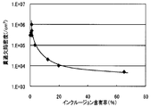
- FIG. 2 shows that it is difficult to produce a crystal having a sufficiently low inclusion content and a sufficiently low penetration defect density.
- the term “smooth” means that no step due to macrosteps or three-dimensional growth is observed on the surface of the crystal except the outer periphery of 5 mm, or the interval is 10 mm even if macrosteps or three-dimensional growth is observed. Or the difference (R pv ) between the highest height position and the lowest height position of the crystal surface is 0.1 mm or less. .
- vigorous stirring refers to a stirring operation that speeds up the flow of the raw material melt in the container by rotating the container at a high speed or changing the stirring speed and direction in a short cycle
- gentle agitation is an agitation operation that slowly convects the raw material melt in the vessel by rotating the vessel at a low speed or by increasing the change interval of the agitation speed or direction.
- the method for growing a group 3B nitride crystal of the present invention is as follows.
- the seed crystal substrate is immersed in a mixed melt containing a group 3B metal and a flux, and a crystal of group 3B nitride is grown on the seed crystal substrate while being heated in a pressurized atmosphere containing nitrogen gas and not oxygen gas.
- a method of growing a group 3B nitride crystal The group 3B nitride crystal is grown by adopting the first stirring condition set so that the growth surface is uneven as the stirring condition of the mixed melt, and then grown as the stirring condition of the mixed melt.
- the group 3B nitride crystal is grown by adopting the second stirring condition set so that the surface is smooth.
- examples of the group 3B nitride include boron nitride (BN), aluminum nitride (AlN), gallium nitride (GaN), indium nitride (InN), and thallium nitride (TlN). preferable.
- the seed crystal substrate for example, a sapphire substrate, a silicon carbide substrate, a silicon substrate or the like on which a thin film of the same type as the Group 3B nitride is formed may be used, or the same type as the Group 3B nitride may be used.
- a substrate may be used.
- the second stirring condition may be milder than the first stirring condition.
- a condition that the stirring direction is reversed every first predetermined time as the first stirring condition is adopted, and the stirring direction is reversed every second predetermined time that is longer than the first predetermined time as the second stirring condition.
- a condition of rotating in one direction at a rotation speed of 2 may be employed.
- the first and second stirring conditions are not limited to this, and the first stirring condition may be any condition as long as the growth surface is uneven, and the second stirring condition is because the growth surface is smooth. Any conditions are acceptable.
- the first stirring condition is employed to grow a Group 3B nitride crystal
- the second stirring condition is employed to form a Group 3B nitride crystal.
- the operation of growing may be one cycle, and this may be repeated two or more cycles.
- the 3B group nitride crystal is grown by adopting the first stirring condition in the second cycle and thereafter, the base is not the seed crystal substrate, and the second stirring condition is adopted in the previous cycle. Since the grown crystal layer has few through defects, dislocation defects are reduced. Therefore, in the next crystal growth under the second stirring condition, a group 3B nitride crystal with fewer through defects can be obtained.
- the first stirring condition is employed to grow the Group 3B nitride crystal, and then the pressure is applied to the seed crystal substrate on which the grown crystal is stacked. Take out from the atmosphere to the atmosphere, flatten the surface so that the surface roughness Ra is 1.5 ⁇ m or less, wash the crystal substrate that has been flattened, and oxidize the Group 3B metal oxide and / or flux Then, the seed crystal substrate may be returned to the pressurized atmosphere and the second stirring condition may be adopted to grow the group 3B nitride crystal.
- the second stirring condition is then used to Even if the crystal is grown, a non-smooth portion may be generated on the growth surface and the crystal quality may deteriorate.
- the growth surface is Since flattening is performed and oxide is removed, the entire surface is smoothly grown with good reproducibility when the second stirring condition is employed to grow a crystal, and the defect occurrence rate is reduced.
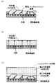
- FIG. 3 shows an example of a specific procedure of the 3B group nitride crystal growth method of the present invention including the surface flattening and the oxide cleaning.
- crystals are grown under the first stirring condition (see FIG. 3A).
- foreign matter (inclusion) is mixed in a part of the grain boundary.
- the crystal is taken out into the atmosphere and the surface is flattened (see FIG. 3B).
- the foreign matter (inclusion) is oxidized to become a Group 3B metal oxide or a flux oxide.
- the flat processing can be performed using a known polishing apparatus such as a lapping apparatus or a CMP (Chemical Mechanical Polishing) apparatus.
- CMP Chemical Mechanical Polishing
- the surface roughness Ra of the surface after flattening is preferably 1.5 ⁇ m or less, and more preferably 0.6 ⁇ m or less. When the surface roughness Ra exceeds 1.5 ⁇ m, the amount of dislocation may increase when the crystal is grown under the second stirring condition, which is not preferable.
- the surface oxide layer and the work-affected layer may be removed by dry etching.
- the flattened surface is cleaned to remove the oxide of the group 3B metal and / or the oxide of the flux (see FIG. 3C).
- removal of the oxide includes, for example, heat treatment or washing with an alkali solution or an acid solution.
- the group 3B nitride crystal of the present invention is A 3B group nitride crystal having an alkali metal content of SIMS below the detection limit; A first crystal layer in which a grain boundary exists in a direction intersecting with an extension direction of defects in the seed crystal substrate when the cross section is viewed; It is laminated on the first crystal layer, and when viewed in cross section, there are few or no grain boundaries as compared to the first crystal layer, and the etch pit density (EPD) is 10 4 / cm 2 or less. A second crystal layer having a region of It is equipped with.
- This 3B group nitride crystal can be obtained by the above-described 3B group nitride crystal growth method.
- the detection limit of SIMS although there are some variations by measuring apparatus and measurement conditions, for lithium about 10 15 atoms / cm 3, from about 10 15 atoms / cm 3 for sodium. Then, if a 3B group nitride wafer is produced from the second crystal layer (see FIG. 1C), a high-quality wafer that has low defects and hardly contains alkali metals such as grain boundaries, inclusions, and lithium can be obtained. It is done.
- the wafer thus obtained can be used for, for example, a high color rendering white LED called a post fluorescent lamp, a blue-violet laser for high-speed and high-density optical memory, and a power device used for an inverter for a hybrid vehicle.
- a high color rendering white LED called a post fluorescent lamp
- a blue-violet laser for high-speed and high-density optical memory
- a power device used for an inverter for a hybrid vehicle for, for example, a high color rendering white LED called a post fluorescent lamp, a blue-violet laser for high-speed and high-density optical memory, and a power device used for an inverter for a hybrid vehicle.
- FIG. 1 It is a schematic diagram of a cross section of a gallium nitride crystal, (a) is a crystal obtained when the mixed melt is vigorously stirred, (b) is a crystal obtained when the mixed melt is gently stirred, (c) is The crystals obtained when the mixed melt is vigorously stirred and then gently stirred are shown. It is a graph which shows the relationship between the content rate of the inclusion contained in a crystal
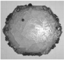
- FIG. 2 is an appearance photograph of the gallium nitride crystal obtained in Example 1.
- FIG. 2 is a fluorescence micrograph of a cross section of a gallium nitride crystal plate obtained in Example 1.
- FIG. 2 is an appearance photograph of a gallium nitride crystal obtained in Comparative Example 1.
- 3 is a fluorescence micrograph of a cross section of a gallium nitride crystal plate obtained in Comparative Example 1.
- FIG. 4 is an appearance photograph of a gallium nitride crystal obtained in Comparative Example 2.
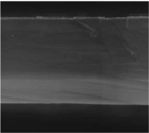
- 7 is a photograph of a transmission light microscope image, differential interference image, and fluorescence microscope image of a cross section of the gallium nitride crystal obtained in Example 5.
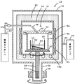
- FIG. 4 is an explanatory diagram (cross-sectional view) showing the overall configuration of the crystal plate manufacturing apparatus 10.
- the crystal plate manufacturing apparatus 10 includes a pressure vessel 12 that can be evacuated or supplied with pressurized nitrogen gas, and a turntable 30 that can rotate within the pressure vessel 12. And an outer container 42 placed on the turntable 30.
- the pressure vessel 12 is formed in a cylindrical shape whose upper and lower surfaces are discs, and has a heating space 16 surrounded by a heater cover 14 inside.
- the internal temperature of the heating space 16 can be adjusted by an upper heater 18a, a middle heater 18b, and a lower heater 18c arranged in the vertical direction of the side surface of the heater cover 14, and a bottom heater 18d arranged on the bottom surface of the heater cover 14. It has become.
- the heating space 16 has enhanced heat insulation properties by a heater heat insulating material 20 that covers the periphery of the heater cover 14.
- the pressure vessel 12 is connected with a nitrogen gas pipe 24 of a nitrogen gas cylinder 22 and a vacuum drawing pipe 28 of a vacuum pump 26.
- the nitrogen gas pipe 24 passes through the pressure vessel 12, the heater heat insulating material 20, and the heater cover 14 and opens into the heating space 16.
- the nitrogen gas pipe 24 is branched in the middle and is also opened in the gap between the pressure vessel 12 and the heater heat insulating material 20.
- a mass flow controller 25 capable of adjusting the flow rate is attached to a branch pipe communicating with the inside of the heating space 16 in the nitrogen gas pipe 24.
- the evacuation pipe 28 penetrates the pressure vessel 12 and opens in a gap between the pressure vessel 12 and the heater heat insulating material 20.
- the turntable 30 is formed in a disk shape and is disposed below the heating space 16.
- a rotating shaft 34 having an internal magnet 32 is attached to the lower surface of the turntable 30.
- the rotating shaft 34 passes through the heater cover 14 and the heater heat insulating material 20 and is inserted into a cylindrical casing 36 integrated with the lower surface of the pressure vessel 12.
- a cylindrical external magnet 38 is rotatably disposed on the outer periphery of the casing 36 by a motor (not shown).
- the external magnet 38 faces the internal magnet 32 of the rotating shaft 34 through the casing 36. For this reason, as the external magnet 38 rotates, the rotary shaft 34 having the internal magnet 32 rotates, and as a result, the turntable 30 rotates. Further, as the external magnet 38 moves up and down, the rotating shaft 34 having the internal magnet 32 moves up and down, and as a result, the turntable 30 moves up and down.
- the outer container 42 has a bottomed cylindrical metal outer container body 44 and a metal outer container lid 46 that closes the upper opening of the outer container body 44.
- a nitrogen introduction pipe 48 is attached to the outer container lid 46 obliquely upward from the center of the lower surface.
- the nitrogen introduction pipe 48 is designed so that it does not collide with the nitrogen gas pipe 24 even if the outer container 42 rotates and comes closest to the nitrogen gas pipe 24 as the turntable 30 rotates. Specifically, the distance between the two when the nitrogen introduction pipe 48 is closest to the nitrogen gas pipe 24 is set to several mm to several tens cm.
- a growing container 50 made of alumina having a bottomed cylindrical shape is disposed inside the outer container main body 44.
- a disc-shaped alumina seed crystal substrate tray 52 is disposed in the growth container 50.
- This seed crystal substrate tray 52 has a recess for fitting a disc-shaped seed crystal substrate 54 at the center, one end is placed on the tray base 56, and the other end is in contact with the bottom surface of the growth vessel 50.
- the seed crystal substrate 54 may be a sapphire substrate having a 3B group nitride thin film formed thereon, or a 3B group nitride thin plate.
- the 3B group metal and the flux are accommodated in the growth container 50.
- the flux alkali metals are preferable, metal sodium and metal potassium are more preferable, and metal sodium is still more preferable.
- the group 3B metal or flux becomes a mixed melt by heating.
- the outer container 42 and the growth container 50 are arranged so as to be coaxial with the rotation center of the turntable 30. For this reason, during rotation, the mixed melt in the growth vessel 50 rotates in the horizontal direction and does not shake significantly in the vertical direction.
- This crystal plate manufacturing apparatus 10 is used for manufacturing a group 3B nitride by a flux method.
- a gallium nitride crystal plate is manufactured as the group 3B nitride crystal plate
- a GaN template (EPD is about 10 8 / cm 2 ) obtained by growing a seed crystal by a vapor phase method
- metal gallium is prepared as a 3B group metal
- metal sodium is prepared as a flux.
- the seed crystal substrate 54 is immersed in a mixed melt containing metal gallium and metal sodium in the growth vessel 50, and the turntable 30 is rotated under the first stirring condition set so that the growth surface is uneven.
- a gallium nitride crystal is grown on the seed crystal substrate 54 in the mixed melt by supplying pressurized nitrogen gas to the mixed melt while heating the heating space 16 in 18a to 18d.
- the stirring condition is changed to the second stirring condition set so that the growth surface is smooth, and a gallium nitride crystal is grown. In this state, the second holding time that is longer than the first holding time is held.
- the gallium nitride crystal plate thus obtained includes a first crystal layer grown on the seed crystal substrate 54, and a second crystal layer grown smoothly on the first crystal layer. It will be.
- the first crystal layer is a crystal layer with many grain boundaries and inclusions but few dislocation defects.
- the second crystal layer has fewer dislocations than the case where the first crystal layer has less dislocations than the seed crystal substrate 54 and is directly grown on the seed crystal substrate 54, and has fewer grain boundaries and inclusions.
- the inclusion content of the second crystal layer is 0 to 10% (0 to 2% depending on the growth conditions).
- the inclusion content ratio is an occupancy ratio of the area of the black portion of the binary image obtained by performing binarization processing on the image taken after polishing the plate surface of the gallium nitride crystal plate.
- the heating temperature is set to be equal to or lower than the boiling point of the mixed melt in a pressurized nitrogen gas atmosphere.
- the temperature is preferably set to 700 to 1000 ° C., more preferably 800 to 900 ° C.
- the upper heater 18a, the middle heater 18b, the lower heater 18c, and the bottom heater 18d are set to increase in temperature in this order, or the upper heater 18a and the middle heater 18b are set to the same temperature T1.
- the lower heater 18c and the bottom heater 18d are set to a temperature T2 higher than the temperature T1.
- the pressure of the pressurized nitrogen gas is preferably set to 1 to 7 MPa, more preferably 2 to 6 MPa.
- the vacuum pump 26 is driven and the internal pressure of the pressure-resistant vessel 12 is set to a high vacuum state (for example, 1 Pa or less or 0.1 Pa or less) through the vacuuming pipe 28.
- the vacuuming pipe 28 is closed by a valve (not shown), and nitrogen gas is supplied from the nitrogen gas cylinder 22 to the inside and outside of the heater cover 14 through the nitrogen gas pipe 24.
- the nitrogen gas is dissolved in the mixed melt and consumed by the crystal growth, and the pressure of the pressurized nitrogen gas decreases.
- the nitrogen gas is supplied to the heating space 16 during the crystal growth. 25, the supply is continued at a predetermined flow rate. During this time, the branch pipe that communicates with the outside of the heater cover 14 in the nitrogen gas pipe 24 is closed by a valve (not shown).
- the first stirring condition may be set so that the growth surface is uneven
- the second stirring condition is that the growth surface is crystallized under the first stirring condition.
- the stirring mode include one-way rotation, rotation with inversion, and intermittent rotation.
- the intermittent rotation includes an operation of alternately repeating one-way rotation and stop, an operation of repeating one-way rotation ⁇ stop ⁇ reverse direction rotation ⁇ stop, and an operation of alternately repeating high-speed rotation and low-speed rotation.
- the stirring mode may be the same or different between the first and second stirring conditions.
- a condition that the stirring direction is reversed every first predetermined time is adopted as the first stirring condition, and the second stirring condition is set as the second stirring condition.
- a condition of rotating in one direction at the first rotation speed as the first stirring condition is adopted, and rotating in one direction at a second rotation speed that is slower than the first rotation speed as the second stirring condition. Conditions may be employed.
- the first stirring condition a condition is adopted in which the first stirring speed is rotated in one direction, then the first resting time is stopped, and then the first stirring speed is rotated again.
- a condition a condition may be adopted in which a rotation is performed in one direction at a second rotation speed that is slower than the first rotation speed, then is stopped for a second pause time, and then rotated again at the second rotation speed.
- a condition that the stirring direction is periodically reversed is adopted as the first stirring condition, and stirring is performed in one direction as the second stirring condition. The above condition may be adopted.
- a condition of stirring in one direction may be employed as the first stirring condition, and a condition of periodically reversing the stirring direction may be employed as the second stirring condition.
- the step of growing crystals while stirring under the first stirring condition and the step of growing crystals while stirring under the second stirring condition may be one cycle, and this may be repeated two or more cycles.
- the first and second stirring conditions are not limited to those exemplified here, and the first stirring conditions may be any conditions as long as the growth surface is set to be uneven.
- the stirring condition 2 may be any condition as long as the growth surface is set to be smoother than the growth surface when the crystal is grown under the first stirring condition.
- the second stirring condition is set so that the growth surface is smooth, but the crystal growth rate of gallium nitride is preferably set to 5 to 25 ⁇ m / h, and preferably 10 to 25 ⁇ m / h. It is more preferable to set. If the crystal growth rate is less than 5 ⁇ m / h, the crystal growth time becomes excessive, making it difficult to actually manufacture, and if the crystal growth rate exceeds 25 ⁇ m / h, the inclusion content tends to increase, which is not preferable. . Further, when rotating the growth vessel 50 under the second stirring condition, the reversing operation of rotating in one direction without being reversed or rotating in one direction for 1 minute or more and then rotating in the reverse direction for 1 minute or more is repeated.
- the intermittent operation of rotating for 5 seconds or more in one direction, resting for a short period (for example, 0.1 to 2 seconds), and then rotating for 5 seconds or more in the same direction. If the reversal operation or intermittent operation is repeated at a shorter cycle than this, the crystal growth rate becomes too fast and the inclusion content increases, which is not preferable.
- the growth time of the gallium nitride crystal when the second stirring condition is adopted may be appropriately set according to the heating temperature and the pressure of the pressurized nitrogen gas, and may be set within a range of several hours to several hundred hours, for example. .
- the first stirring condition may be set so as to be severer than the second stirring condition.
- the crystal growth rate of gallium nitride it is preferable to be> 25 ⁇ m / h.
- the growth time of the gallium nitride crystal when the first stirring condition is adopted may be appropriately set according to the heating temperature and the pressure of the pressurized nitrogen gas, and may be set within a range of several hours to several tens of hours, for example. .
- the 3B group nitride crystal when the 3B group nitride crystal is grown by adopting the first stirring condition, there are many grain boundaries and inclusions on the seed crystal substrate, but there are few dislocation defects.
- a first crystal layer is formed and then a 3B group nitride crystal is grown using the second stirring condition, there are few penetration defects on the first crystal layer, and there are few grain boundaries and inclusions.
- a second crystalline layer is formed. That is, a group 3B nitride crystal plate in which the first crystal layer and the second crystal layer are stacked in this order on the seed crystal substrate 54 is obtained.
- a group 3B nitride crystal with few penetration defects and few grain boundaries and inclusions can be obtained.
- the seed crystal substrate tray 52 with the seed crystal substrate 54 fitted in the center is used and one end of the seed crystal substrate tray 52 is placed on the tray table 56 and is tilted in the growth container 50, the entire surface of the seed crystal substrate 54 is disposed. In this case, crystal growth is easy to proceed. Since the mixed melt is likely to stagnate at the peripheral edge of the bottom surface of the growth vessel 50, if a part of the seed crystal substrate 54 is located in the vicinity thereof, the crystal growth of that part tends to be insufficient. However, in this embodiment, since the seed crystal substrate tray 52 is used, the seed crystal substrate 54 is not positioned near the bottom edge of the growth vessel 50, and crystal growth proceeds sufficiently on the entire surface of the seed crystal substrate 54. It is.
- the pipe 24 and the pipe 48 do not prevent the outer container 42 from rotating together with the turntable 30.
- the entire heating space 16 can be maintained at a uniform temperature including the vicinity of the bottom surface where the temperature is likely to be non-uniform. .
- the rotating shaft 34 integrated with the internal magnet 32 rotates and moves up and down as the external magnet 38 arranged on the outer periphery of the casing 36 rotates and moves up and down, the inside of the pressure vessel 12 is moved.
- the outer container 42 can be rotated and moved up and down while being kept sealed.
- Example 1 A gallium nitride crystal plate was manufactured using the crystal plate manufacturing apparatus 10 shown in FIG. The procedure will be described in detail below.
- a tray table 56 is placed at one end of a growth container 50 having an inner diameter of 70 mm, and the seed crystal substrate tray 52 is leaned against the tray table 56 so that the angle becomes 10 °.
- a ⁇ ⁇ 2 inch GaN template was placed as a seed crystal substrate 54 in the center of the seed crystal substrate tray 52.
- 60 g of metallic sodium and 40 g of metallic gallium were filled in the growth vessel 50.
- the growing container 50 was placed in the outer container body 44, and the opening of the outer container body 44 was closed with an outer container lid 46 with a nitrogen introduction pipe 48.
- the outer container 42 was placed on a turntable 30 that had been vacuum-baked in advance, and the pressure-resistant container 12 was sealed with a lid (not shown).
- the inside of the pressure vessel 12 was evacuated to 0.1 Pa or less by driving the vacuum pump 26.
- the upper heater 18a, the middle heater 18b, the lower heater 18c, and the bottom heater 18d are adjusted to 855 ° C., 855 ° C., 880 ° C., and 880 ° C., respectively, and the temperature of the heating space 16 is heated to 870 ° C.
- the nitrogen gas was introduced from the nitrogen gas cylinder 22 up to 4.5 MPa.
- the outer container 42 was rotated around the central axis. The rotation speed was 30 rpm and reversed every 15 seconds. After holding in this state for 24 hours, the inversion period was changed to 5 minutes, and further maintained for 130 hours.
- the first stirring condition is reversed every 15 seconds at a rotation speed of 30 rpm
- the second stirring condition is reversed every 5 minutes at a rotation speed of 30 rpm.
- the lid of the pressure vessel 12 is opened, the growth vessel 50 is taken out from the inside, ethanol is poured into the growth vessel 50, metal sodium is dissolved in ethanol, and then the grown gallium nitride crystal plate is It was collected.
- the size of this gallium nitride crystal plate was ⁇ 2 inches, the thickness was about 2 mm, and the crystal growth rate was about 13 ⁇ m / h. Although the thickness was almost uniform, shallow irregularities with a step of 30 ⁇ m or less were observed near the outer periphery of the crystal surface. An appearance photograph of the crystal is shown in FIG.
- Elemental analysis by SIMS was performed using a part of this gallium nitride crystal plate (a part without inclusion).
- the content of alkali metals such as Li, Na and K was below the lower limit of detection.
- the content of alkaline earth metals such as Mg and Ca was below the lower limit of detection.
- C and O were also below the lower limit of detection.
- Table 1 All units are atoms / cm 3 .
- the portion close to the surface of the gallium nitride crystal plate is polished so as to have a thickness of 500 ⁇ m, the photographed image is subjected to binarization processing, and the inclusion in the 70% region excluding the outer peripheral portion of the seed crystal substrate 54 is processed.
- the area (the area of the black portion of the binary image) was determined, and the ratio of the area of inclusion to the entire 70% region, that is, the inclusion content was calculated.
- the inclusion content was 0 to 10%.
- the EPD was 10 4 / cm 2 or less over almost the entire area excluding the outer periphery.
- Example 2 A gallium nitride crystal was grown under the same conditions as in Example 1. However, after holding the inversion cycle of the outer container 42 for 15 hours for 24 hours, switching the inversion cycle to 5 minutes and holding it for 6 hours, again switching the inversion cycle to 15 seconds and holding it for 6 hours, then inversion again The cycle was switched to 5 minutes and held for 120 hours.
- the size of the obtained gallium nitride crystal was ⁇ 2 inches, the thickness was 2.3 mm, and the crystal growth rate was about 15 ⁇ m / h.
- the crystal surface was smooth. When the cross-section was observed in the same manner as in Example 1, three changes in the growth history during the crystal growth were observed.
- the alkali metal content was not more than the lower limit of detection. Further, when the polishing process was performed in the same manner as in Example 1 and the inclusion content was evaluated by image processing, the inclusion content was 0 to 10%. Furthermore, when the EPD was evaluated in the same manner as in Example 1, the EPD was 10 4 / cm 2 or less in almost the entire region, and was partially dislocation-free.
- Example 3 Gallium nitride crystals were grown under the same conditions as in Example 1. However, after holding the inversion cycle of the outer container 42 for 15 seconds for 24 hours, the rotation speed was fixed at 30 rpm, and the rotation was performed in one direction for 130 hours. The size of the obtained gallium nitride crystal was ⁇ 2 inches, the thickness was about 2 mm, and the crystal growth rate was about 13 ⁇ m / h. The crystal surface was mostly smooth, but some irregularities were observed in the vicinity of the outer periphery. When a cross-sectional observation was performed in the same manner as in Example 1, a change in growth history was observed in a portion corresponding to the change in the rotation condition.
- the inclusion content was 0 to 10%.
- the EPD was 10 4 / cm 2 or less in almost the entire region except the outer peripheral portion.
- Example 4 A gallium nitride crystal was grown under the same conditions as in Example 1. However, when rotating the outer container 42, first hold for 10 seconds at a rotation speed of 6 rpm, then change the rotation speed to 60 rpm without stopping and hold for another 10 seconds, then return to 6 rpm again and hold for 10 seconds, Further, the combination of returning to 60 rpm and holding for 10 seconds was repeated for 24 hours, and then the rotation speed was fixed at 30 rpm and rotated in one direction for 130 hours.
- the size of the obtained gallium nitride crystal was ⁇ 2 inches, the thickness was about 1.8 mm, and the crystal growth rate was about 12 ⁇ m / h.
- the crystal surface was generally smooth.
- Example 1 When a cross-sectional observation was performed in the same manner as in Example 1, a change in growth history was observed in a portion corresponding to the change in the rotation condition. Further, when the polishing process was performed in the same manner as in Example 1 and the inclusion content was evaluated by image processing, the inclusion content was 0 to 10%. When the EPD was evaluated in the same manner as in Example 1, the EPD was 10 4 / cm 2 or less in almost the entire region except the outer peripheral portion.
- Example 1 A gallium nitride crystal was grown under the same conditions as in Example 1. However, the inversion period of the outer container 42 was fixed to 15 seconds through the growth and was not changed in the middle. The size of the obtained gallium nitride crystal was ⁇ 2 inches, the thickness was about 4 mm, and the crystal growth rate was about 26 ⁇ m / h. Stepped irregularities were found in a wide area of the crystal surface. An appearance photograph of the crystal is shown in FIG. When the cross section was observed in the same manner as in Example 1, no clear change in the growth history during the crystal growth was observed. Inclusion was observed during growth. A cross-sectional fluorescence micrograph is shown in FIG.
- Example 2 polishing was performed in the same manner as in Example 1, and the inclusion content was evaluated by image processing. As a result, the inclusion content was 6 to 30%. Furthermore, when the EPD was evaluated in the same manner as in Example 1, the EPD was about 10 4 / cm 2 or less in an area of about 90%.
- Example 2 A gallium nitride crystal was grown under the same conditions as in Example 1. However, the inversion period of the outer container 42 was fixed to 5 minutes throughout the growth and was not changed in the middle. The size of the obtained gallium nitride crystal was ⁇ 2 inches, the thickness was about 1.8 mm, and the crystal growth rate was about 12 ⁇ m / h. The crystal surface was smooth throughout. An appearance photograph of the crystal is shown in FIG. When the cross section was observed in the same manner as in Example 1, no clear change in the growth history during the crystal growth was observed. Further, polishing was performed in the same manner as in Example 1, and the inclusion content was evaluated by image processing. As a result, the inclusion content was 0 to 1%. Further, when the EPD was evaluated in the same manner as in Example 1, the EPD was in the range of 10 5 to 10 6 / cm 2 in the region of about 90%.
- Example 5 A gallium nitride crystal was grown according to the specific procedure of FIG.
- the first and second stirring conditions were the same as those in Example 1.
- the outer container 42 was cooled, and the seed crystal substrate 54 on which the grown crystal was laminated was taken out into the atmosphere.
- the size of the obtained gallium nitride crystal was ⁇ 2 inches, the thickness was 1.3 mm, and the crystal growth rate was about 22 ⁇ m / h. Stepped irregularities were found in a wide area of the crystal surface.
- the surface of the crystal was smoothed by polishing.
- the crystal was subjected to acetone ultrasonic cleaning, then alcohol ultrasonic cleaning, then pure water ultrasonic cleaning, and then nitrogen blowing. Furthermore, heat treatment was performed at 1000 ° C. in a nitrogen atmosphere. Further, it was washed with an aqueous potassium hydroxide solution, then ultrasonically cleaned with pure water and then blown with nitrogen. Further, the surface was ashed with a nitrogen plasma asher. By executing these treatments, organic substances on the crystal surface, Na compound, Ga compound, residual carbon and the like were removed. Further, the surface oxide layer and the work-affected layer were removed by dry etching. After that, the crystal is put in the outer container 42 and placed in the crystal plate manufacturing apparatus 10 again.
- FIG. 10 shows a transmission light microscope image (see FIG. 10A), a differential interference image (see FIG. 10B), and a fluorescence microscope image (FIG.
- Example 10C of the cross section of the gallium nitride crystal obtained in Example 5. )).
- LPE is an abbreviation for Liquid Phase Epitaxy. Further, only the region above the polished surface was taken out by processing, and the inclusion content was evaluated by image processing in the same manner as in Example 1. The inclusion content was 0 to 10%. When EPD was evaluated in the same manner as in Example 1, the EPD was 10 4 / cm 2 or less in almost the entire region except the outer peripheral portion.
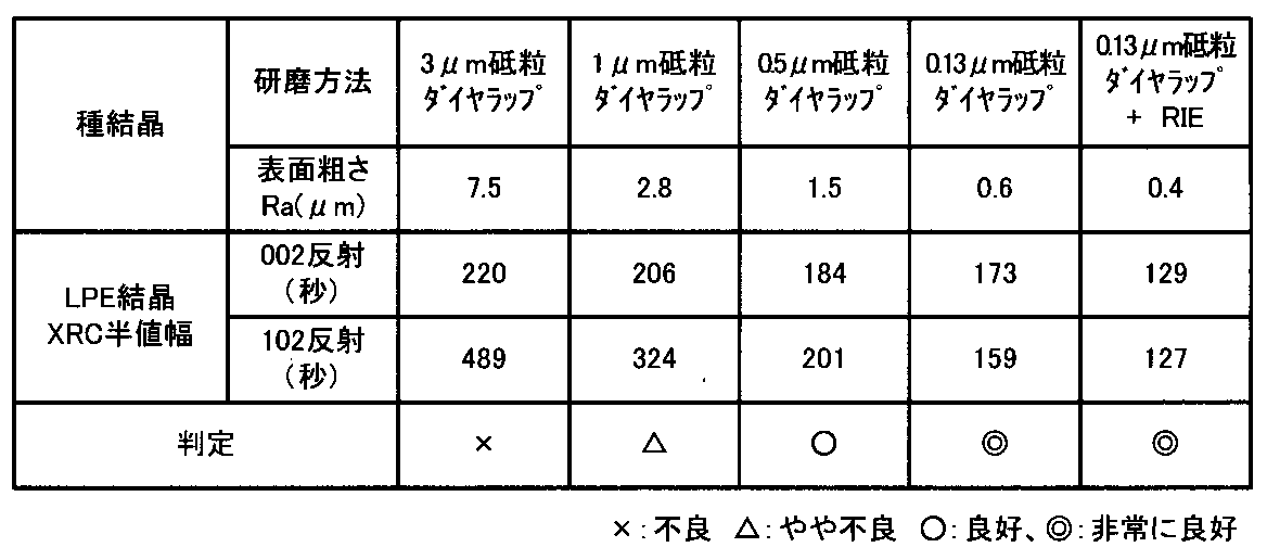
- Reference Examples 1--5 As a seed crystal, a GaN substrate produced by a vapor phase growth method was used, and the relationship between the surface roughness Ra and the quality of the LPE crystal was investigated.
- the GaN substrate used here has dislocations but is almost free of foreign matter in the grain boundary, and is the same as the crystal obtained by growing the gallium nitride crystal under the first stirring condition in Example 5. I was able to see.
- the GaN substrate was polished by the polishing method shown in Table 2 so that the surface roughness Ra was 0.4 to 7.5 ⁇ m, and then the second stirring condition of Example 5 Gallium nitride crystals were grown under the same conditions.
- the XRC half-width was examined. The results are shown in Table 2. As is clear from Table 2, it can be seen that the XRC half-value width becomes narrower as the surface roughness Ra becomes smaller. Specifically, when the surface roughness Ra was 1.5 ⁇ m, high quality crystals with a relatively small amount of dislocation were obtained, and when the surface roughness Ra was 0.6 ⁇ m and 0.4 ⁇ m, higher quality crystals were obtained. For these reasons, the surface roughness Ra is preferably 1.5 ⁇ m or less in flat processing.
- the narrower the XRC half-width the smaller the dislocation amount, the higher the quality crystal, but the dislocation amount in the grown gallium nitride crystal does not fall below the amount present in the seed crystal.
- the present invention can be used for a method of manufacturing a semiconductor device such as a blue LED, a white LED, or a blue-violet semiconductor laser in addition to a high-frequency device typified by a power amplifier.
- a semiconductor device such as a blue LED, a white LED, or a blue-violet semiconductor laser in addition to a high-frequency device typified by a power amplifier.
Landscapes
- Chemical & Material Sciences (AREA)
- Engineering & Computer Science (AREA)
- Crystallography & Structural Chemistry (AREA)
- Materials Engineering (AREA)
- Metallurgy (AREA)
- Organic Chemistry (AREA)
- Inorganic Chemistry (AREA)
- Crystals, And After-Treatments Of Crystals (AREA)
- Liquid Deposition Of Substances Of Which Semiconductor Devices Are Composed (AREA)
Abstract
Description
種結晶基板を3B族金属及びフラックスを含む混合融液に浸漬して窒素ガスを含み酸素ガスを含まない加圧雰囲気下で加熱した状態で前記種結晶基板上に3B族窒化物の結晶を成長させる3B族窒化物の結晶成長方法であって、
前記混合融液の攪拌条件として成長面が凹凸となるように設定された第1の攪拌条件を採用して前記3B族窒化物の結晶を成長させ、次に前記混合融液の攪拌条件として成長面が平滑となるように設定された第2の攪拌条件を採用して前記3B族窒化物の結晶を成長させるものである。
アルカリ金属の含有率がSIMSで検出下限以下の3B族窒化物結晶であって、
断面をみたときに種結晶基板内の欠陥の伸長方向と交差する方向に粒界が存在する第1結晶層と、
前記第1結晶層上に積層され、断面をみたときに前記第1結晶層に比べて前記粒界が少ないか存在せず、エッチピット密度(Etch pit density,EPD)が104/cm2以下の領域を有する第2結晶層と、
を備えたものである。
図4に示す結晶板製造装置10を用いて、窒化ガリウム結晶板を作製した。以下、その手順を詳説する。

実施例1と同様の条件で窒化ガリウム結晶の育成を行った。但し、外容器42の反転周期を15秒として24時間保持したあと、反転周期を5分に切り替えて6時間保持し、再度、反転周期を15秒に切り替えて6時間保持してから、もう一度反転周期を5分に切り替えて120時間保持した。得られた窒化ガリウム結晶の大きさはφ2インチであり、厚さは2.3mmであり、結晶成長速度は約15μm/hであった。結晶表面は平滑であった。実施例1と同様に断面観察を行ったところ、結晶成長途中での3回の成長履歴の変化が観察された。実施例1と同様にSIMS分析を行ったところ、アルカリ金属の含有量は検出下限以下であった。また、実施例1と同様に研磨加工を行い、画像処理によりインクルージョン含有率の評価を行ったところ、インクルージョン含有率は0~10%であった。更に、実施例1と同様にEPDの評価をしたところ、EPDはほぼ全域で104/cm2台以下であり、部分的には無転位であった。
実施例1と同様の条件で窒化ガリウム結晶の育成を行った。但し、外容器42の反転周期を15秒として24時間保持したあと、回転速度を30rpmに固定して一方向に回転させ130時間保持した。得られた窒化ガリウム結晶の大きさはφ2インチであり、厚さは約2mmであり、結晶成長速度は約13μm/hであった。結晶表面は大部分が平滑であったが、外周部の近傍に若干の凹凸が観察された。実施例1と同様に断面観察を行ったところ、回転条件の変更に該当する部分で、成長履歴の変化が観察された。また、実施例1と同様に研磨加工を行い、画像処理によりインクルージョン含有率の評価を行ったところ、インクルージョン含有率は0~10%であった。実施例1と同様にEPDの評価をしたところ、EPDは外周部を除くほぼ全域で104/cm2台以下であった。
実施例1と同様の条件で窒化ガリウム結晶の育成を行った。但し、外容器42を回転するにあたり、まず回転速度6rpmで10秒間保持した後、停止することなく回転速度を60rpmに変更してさらに10秒間保持し、その後再び6rpmに戻して10秒間保持し、更にまた60rpmに戻して10秒間保持・・・、という組合せを24時間繰り返した後、回転速度を30rpmに固定して一方向に回転させ130時間保持した。得られた窒化ガリウム結晶の大きさはφ2インチであり、厚さは約1.8mmであり、結晶成長速度は約12μm/hであった。結晶表面はおおむね平滑であった。実施例1と同様に断面観察を行ったところ、回転条件の変更に該当する部分で、成長履歴の変化が観察された。また、実施例1と同様に研磨加工を行い、画像処理によりインクルージョン含有率の評価を行ったところ、インクルージョン含有率は0~10%であった。実施例1と同様にEPDの評価をしたところ、EPDは外周部を除くほぼ全域で104/cm2台以下であった。
実施例1と同様の条件で窒化ガリウム結晶の育成を行った。但し、外容器42の反転周期は育成を通じて15秒に固定し、途中で変化させなかった。得られた窒化ガリウム結晶の大きさはφ2インチであり、厚さは約4mmであり、結晶成長速度は約26μm/hであった。結晶表面の広い範囲に階段状の凹凸が見られた。結晶の外観写真を図7に示す。実施例1と同様に断面観察を行ったところ、結晶成長途中での明確な成長履歴の変化は見られなかった。成長途中でインクルージョンの発生が認められた。断面の蛍光顕微鏡写真を図8に示す。また、実施例1と同様に研磨加工を行い、画像処理によりインクルージョン含有率の評価を行ったところ、インクルージョン含有率は6~30%であった。更に、実施例1と同様にEPDの評価をしたところ、EPDは約90%の領域で104/cm2台以下であった。
実施例1と同様の条件で窒化ガリウム結晶の育成を行った。但し、外容器42の反転周期は育成を通じて5分に固定し、途中で変化させなかった。得られた窒化ガリウム結晶の大きさはφ2インチであり、厚さは約1.8mmであり、結晶成長速度は約12μm/hであった。結晶表面は全域で平滑であった。結晶の外観写真を図9に示す。実施例1と同様に断面観察を行ったところ、結晶成長途中での明確な成長履歴の変化は見られなかった。また、実施例1と同様に研磨加工を行い、画像処理によりインクルージョン含有率の評価を行ったところ、インクルージョン含有率は0~1%であった。更に、実施例1と同様にEPDの評価をしたところ、EPDは約90%の領域で105~106/cm2台であった。
図2の具体的手順にしたがって窒化ガリウム結晶を育成した。なお、第1及び第2の攪拌条件は、実施例1と同様の条件を採用した。まず、第1の攪拌条件での窒化ガリウム結晶の育成を60時間行った後、外容器42を冷却し、成長した結晶が積層した種結晶基板54を大気中に取り出した。得られた窒化ガリウム結晶の大きさはφ2インチであり、厚さは1.3mmであり、結晶成長速度は約22μm/hであった。結晶表面の広い範囲に階段状の凹凸が見られた。次に、この結晶の表面を研磨加工により平滑にした。研磨後の結晶の厚さは1.0mmであり、表面粗さはRa=0.4nmであった。次に、この結晶をアセトン超音波洗浄、次いでアルコール超音波洗浄、次いで純水超音波洗浄、次いで窒素ブローした。さらに、窒素雰囲気下で1000℃に加熱処理した。さらに水酸化カリウム水溶液で洗浄し、次いで純水超音波洗浄、次いで窒素ブローした。さらに窒素プラズマアッシャーで表面をアッシング処理した。これらの処理を実行することにより、結晶表面の有機物やNa化合物、Ga化合物、残留炭素などが除去された。さらにドライエッチングにより表面酸化層及び加工変質層を除去した。その後、この結晶を外容器42に入れ、再度結晶板製造装置10に設置し、第2の撹拌条件での窒化ガリウム結晶の育成を100時間行った後、外容器42を冷却して結晶を取り出した。得られた窒化ガリウム結晶の再成長厚さは1.2mmであり、成長速度は12μm/hであった。また、結晶表面は平滑であった。得られた窒化ガリウム結晶につき、実施例1と同様に断面観察を行ったところ、研磨面より下部にはインクルージョンの取り込みを伴う粒界が多数観察されたが、研磨面より上部にはインクルージョンや粒界は観察されなかった。図10に、実施例5で得られた窒化ガリウム結晶の断面の透過光顕微鏡像(図10(a)参照)、微分干渉像(図10(b)参照)、蛍光顕微鏡像(図10(c)参照)を示す。図10中、LPEはLiquid Phase Epitaxyの略である。また、研磨面より上部の領域のみを加工により取り出し、実施例1と同様に画像処理によりインクルージョン含有率の評価を行ったところ、インクルージョンの含有率は0~10%であった。実施例1と同様にEPDを評価したところ、EPDは外周部を除くほぼ全域で104/cm2台以下であった。
種結晶として、気相成長法で作製したGaN基板を使用し、表面粗さRaとLPE結晶の品質との関係を調査した。ここで使用したGaN基板は、転位は存在するものの、粒界中に異物がほとんどないものであることから、実施例5の第1の攪拌条件での窒化ガリウム結晶の育成によって得られる結晶と同一視できるとした。参考例1~5では、GaN基板を表2に示す研磨方法で研磨して、表面粗さRaが0.4~7.5μmとなるようにしたあと、実施例5の第2の攪拌条件と同じ条件で窒化ガリウム結晶の育成を行った。各参考例で得られた窒化ガリウム結晶につき、XRC半値幅を調べた。その結果を表2に示す。表2から明らかなように、表面粗さRaが小さいほどXRC半値幅が狭くなることがわかる。具体的には、表面粗さRaが1.5μmのときには転位量の比較的少ない高品質な結晶が得られ、0.6μm,0.4μmのときにはより高品質な結晶が得られた。こうしたことから、平坦加工では表面粗さRaを1.5μm以下とすることが好ましい。ここで、XRC半値幅が狭いほど、転位量の少ない高品質な結晶といえるが、育成された窒化ガリウム結晶中の転位量は種結晶に存在していた量を下回ることはない。
Claims (6)
- 種結晶基板を3B族金属及びフラックスを含む混合融液に浸漬して窒素ガスを含み酸素を含まない加圧雰囲気下で加熱した状態で前記種結晶基板上に3B族窒化物の結晶を成長させる3B族窒化物の結晶成長方法であって、
前記混合融液の攪拌条件として成長面が凹凸となるように設定された第1の攪拌条件を採用して前記3B族窒化物の結晶を成長させ、次に前記混合融液の攪拌条件として成長面が平滑となるように設定された第2の攪拌条件を採用して前記3B族窒化物の結晶を成長させる、
3B族窒化物の結晶成長方法。 - 前記第2の攪拌条件は、前記第1の攪拌条件に比べて緩やかな条件である、
請求項1に記載の3B族窒化物の結晶成長方法。 - 前記第1の攪拌条件として第1の所定時間ごとに攪拌方向を反転させるという条件を採用し、前記第2の攪拌条件として前記第1の所定時間より長い第2の所定時間ごとに攪拌方向を反転させるという条件を採用するか、又は、前記第1の攪拌条件として第1の回転速度で一方向に回転させるという条件を採用し、前記第2の攪拌条件として前記第1の回転速度より遅い第2の回転速度で一方向に回転させるという条件を採用する、
請求項1又は2に記載の3B族窒化物の結晶成長方法。 - 前記第1の攪拌条件を採用して前記3B族窒化物の結晶を成長させ、次に前記第2の攪拌条件を採用して前記3B族窒化物の結晶を成長させるという操作を1サイクルとし、これを2サイクル以上繰り返す、
請求項1~3のいずれか1項に記載の3B族窒化物の結晶成長方法。 - 前記第1の攪拌条件を採用して前記3B族窒化物の結晶を成長させた後、該成長した結晶が積層した種結晶基板を前記加圧雰囲気から大気中に取り出し、表面粗さRaが1.5μm以下となるように表面を平坦加工し、更に該結晶基板を洗浄して3B族金属の酸化物及び/又はフラックスの酸化物を除去し、その後、前記種結晶基板を前記加圧雰囲気に戻し、前記第2の攪拌条件を採用して前記3B族窒化物の結晶を成長させる、
請求項1~4のいずれか1項に記載の3B族窒化物の結晶成長方法。 - アルカリ金属の含有率がSIMSで検出下限以下の3B族窒化物結晶であって、
断面をみたときに種結晶基板内の欠陥の伸長方向と交差する方向に粒界が存在する第1結晶層と、
前記第1結晶層上に積層され、断面をみたときに前記第1結晶層に比べて前記粒界が少ないか存在せず、エッチピット密度が104/cm2以下の領域を有する第2結晶層と、
を備えた3B族窒化物結晶。
Priority Applications (4)
| Application Number | Priority Date | Filing Date | Title |
|---|---|---|---|
| CN200980156873.9A CN102317512B (zh) | 2009-02-16 | 2009-12-25 | 13族氮化物的晶体生长方法及13族氮化物晶体 |
| JP2010550423A JP5451651B2 (ja) | 2009-02-16 | 2009-12-25 | 13族窒化物の結晶成長方法及び13族窒化物結晶 |
| US13/208,944 US8440017B2 (en) | 2009-02-16 | 2011-08-12 | Method for growing group 13 nitride crystal and group 13 nitride crystal |
| US13/861,695 US8729672B2 (en) | 2009-02-16 | 2013-04-12 | Method for growing group 13 nitride crystal and group 13 nitride crystal |
Applications Claiming Priority (2)
| Application Number | Priority Date | Filing Date | Title |
|---|---|---|---|
| JP2009-032779 | 2009-02-16 | ||
| JP2009032779 | 2009-02-16 |
Related Child Applications (1)
| Application Number | Title | Priority Date | Filing Date |
|---|---|---|---|
| US13/208,944 Continuation US8440017B2 (en) | 2009-02-16 | 2011-08-12 | Method for growing group 13 nitride crystal and group 13 nitride crystal |
Publications (1)
| Publication Number | Publication Date |
|---|---|
| WO2010092736A1 true WO2010092736A1 (ja) | 2010-08-19 |
Family
ID=42561585
Family Applications (1)
| Application Number | Title | Priority Date | Filing Date |
|---|---|---|---|
| PCT/JP2009/071605 Ceased WO2010092736A1 (ja) | 2009-02-16 | 2009-12-25 | 3b族窒化物の結晶成長方法及び3b族窒化物結晶 |
Country Status (4)
| Country | Link |
|---|---|
| US (2) | US8440017B2 (ja) |
| JP (1) | JP5451651B2 (ja) |
| CN (2) | CN103556225B (ja) |
| WO (1) | WO2010092736A1 (ja) |
Cited By (14)
| Publication number | Priority date | Publication date | Assignee | Title |
|---|---|---|---|---|
| WO2013021804A1 (ja) * | 2011-08-10 | 2013-02-14 | 日本碍子株式会社 | 13族元素窒化物膜の剥離方法 |
| WO2013022122A1 (ja) * | 2011-08-10 | 2013-02-14 | 日本碍子株式会社 | 13族元素窒化物膜およびその積層体 |
| US20130224100A1 (en) * | 2012-02-24 | 2013-08-29 | The Regents Of The University Of California | Electromagnetic mixing for nitride crystal growth |
| JPWO2013022123A1 (ja) * | 2011-08-10 | 2015-03-05 | 日本碍子株式会社 | 半導体発光素子およびこれを含む積層体 |
| WO2017026196A1 (ja) * | 2015-08-10 | 2017-02-16 | 株式会社リコー | 13族窒化物単結晶の製造方法、および13族窒化物単結晶の製造装置 |
| JP2019029568A (ja) * | 2017-08-01 | 2019-02-21 | 株式会社サイオクス | 半導体積層物の製造方法および窒化物結晶基板の製造方法 |
| WO2020045234A1 (ja) * | 2018-08-29 | 2020-03-05 | 株式会社サイオクス | 窒化物半導体基板の製造方法、窒化物半導体基板および積層構造体 |
| WO2020045233A1 (ja) * | 2018-08-29 | 2020-03-05 | 株式会社サイオクス | 窒化物半導体基板の製造方法、窒化物半導体基板および積層構造体 |
| JP2020033212A (ja) * | 2018-08-29 | 2020-03-05 | 株式会社サイオクス | 窒化物半導体基板、窒化物半導体基板の製造方法および積層構造体 |
| JP2020033253A (ja) * | 2019-09-20 | 2020-03-05 | 株式会社サイオクス | 窒化物半導体基板 |
| JP2020070229A (ja) * | 2018-10-26 | 2020-05-07 | 株式会社サイオクス | 窒化物半導体基板の製造方法、窒化物半導体基板および積層構造体 |
| JP2020075837A (ja) * | 2018-11-08 | 2020-05-21 | 株式会社サイオクス | 窒化物半導体基板の製造方法、窒化物半導体基板および積層構造体 |
| JP2020152582A (ja) * | 2019-03-18 | 2020-09-24 | 豊田合成株式会社 | Iii族窒化物半導体の製造方法 |
| JP2020189762A (ja) * | 2019-05-20 | 2020-11-26 | 株式会社サイオクス | 窒化物半導体基板の製造方法、窒化物半導体基板および積層構造体 |
Families Citing this family (10)
| Publication number | Priority date | Publication date | Assignee | Title |
|---|---|---|---|---|
| JP6026188B2 (ja) * | 2011-09-12 | 2016-11-16 | 住友化学株式会社 | 窒化物半導体結晶の製造方法 |
| KR102022659B1 (ko) * | 2012-02-20 | 2019-11-04 | 서울바이오시스 주식회사 | 고효율 발광 다이오드 및 그것을 제조하는 방법 |
| WO2014025003A1 (ja) * | 2012-08-06 | 2014-02-13 | 日本碍子株式会社 | 複合基板および機能素子 |
| JP6175817B2 (ja) * | 2013-03-13 | 2017-08-09 | 株式会社リコー | 13族窒化物結晶の製造方法、及び製造装置 |
| JP6155716B2 (ja) * | 2013-03-13 | 2017-07-05 | 株式会社リコー | 13族窒化物結晶、及び13族窒化物結晶の製造方法 |
| JP6714320B2 (ja) * | 2014-03-18 | 2020-06-24 | 株式会社サイオクス | 13族窒化物結晶の製造方法及び13族窒化物結晶を有する積層体 |
| JP6479054B2 (ja) * | 2015-01-29 | 2019-03-06 | 日本碍子株式会社 | 自立基板、機能素子およびその製造方法 |
| CN106637412A (zh) * | 2016-11-14 | 2017-05-10 | 东莞市中镓半导体科技有限公司 | 氮化物晶体的液相生长装置 |
| CN107133466B (zh) * | 2017-04-28 | 2020-08-18 | 郑州大学 | 一种材料结晶过程的计算机数值模拟方法 |
| JP6998798B2 (ja) * | 2018-03-02 | 2022-01-18 | 株式会社サイオクス | GaN積層体およびその製造方法 |
Citations (2)
| Publication number | Priority date | Publication date | Assignee | Title |
|---|---|---|---|---|
| WO2004083498A1 (ja) * | 2003-03-17 | 2004-09-30 | Osaka Industrial Promotion Organization | Iii族元素窒化物単結晶の製造方法およびそれに用いる装置 |
| JP2007277055A (ja) * | 2006-04-07 | 2007-10-25 | Toyoda Gosei Co Ltd | 半導体結晶の製造方法および半導体基板 |
Family Cites Families (2)
| Publication number | Priority date | Publication date | Assignee | Title |
|---|---|---|---|---|
| JP4856934B2 (ja) | 2005-11-21 | 2012-01-18 | 株式会社リコー | GaN結晶 |
| JP5651481B2 (ja) * | 2009-01-23 | 2015-01-14 | 日本碍子株式会社 | 3b族窒化物結晶 |
-
2009
- 2009-12-25 CN CN201310419587.5A patent/CN103556225B/zh active Active
- 2009-12-25 CN CN200980156873.9A patent/CN102317512B/zh active Active
- 2009-12-25 WO PCT/JP2009/071605 patent/WO2010092736A1/ja not_active Ceased
- 2009-12-25 JP JP2010550423A patent/JP5451651B2/ja active Active
-
2011
- 2011-08-12 US US13/208,944 patent/US8440017B2/en active Active
-
2013
- 2013-04-12 US US13/861,695 patent/US8729672B2/en not_active Expired - Fee Related
Patent Citations (2)
| Publication number | Priority date | Publication date | Assignee | Title |
|---|---|---|---|---|
| WO2004083498A1 (ja) * | 2003-03-17 | 2004-09-30 | Osaka Industrial Promotion Organization | Iii族元素窒化物単結晶の製造方法およびそれに用いる装置 |
| JP2007277055A (ja) * | 2006-04-07 | 2007-10-25 | Toyoda Gosei Co Ltd | 半導体結晶の製造方法および半導体基板 |
Non-Patent Citations (2)
| Title |
|---|
| F. KAWAMURA ET AL.: "Growth of a large GaN single crystal using the liquid phase epitaxy (LPE) technique", JAPANESE JOURNAL OF APPLIED PHYSICS, vol. 42, no. 1A/B, 15 January 2003 (2003-01-15), pages L4 - L6 * |
| YUSUKE MORI ET AL.: "Na Flux LPE-ho ni yoru Ogata Kohinshitsu GaN Kessho Ikusei Gijutsu no Genjo to Tenbo", TOYODA GOSEI TECHNICAL REVIEW, vol. 50, no. 1, 2008, pages 2 - 7 * |
Cited By (31)
| Publication number | Priority date | Publication date | Assignee | Title |
|---|---|---|---|---|
| DE112012003278B4 (de) | 2011-08-10 | 2018-08-23 | Ngk Insulators, Ltd. | Filme von Nitriden von Gruppe-13-Elementen und geschichteter Körper, der dieselben beinhaltet |
| WO2013022122A1 (ja) * | 2011-08-10 | 2013-02-14 | 日本碍子株式会社 | 13族元素窒化物膜およびその積層体 |
| CN103237931A (zh) * | 2011-08-10 | 2013-08-07 | 日本碍子株式会社 | 13族元素氮化物膜及其叠层体 |
| WO2013021804A1 (ja) * | 2011-08-10 | 2013-02-14 | 日本碍子株式会社 | 13族元素窒化物膜の剥離方法 |
| JPWO2013021804A1 (ja) * | 2011-08-10 | 2015-03-05 | 日本碍子株式会社 | 13族元素窒化物膜の剥離方法 |
| JPWO2013022123A1 (ja) * | 2011-08-10 | 2015-03-05 | 日本碍子株式会社 | 半導体発光素子およびこれを含む積層体 |
| JPWO2013022122A1 (ja) * | 2011-08-10 | 2015-03-05 | 日本碍子株式会社 | 13族元素窒化物膜およびその積層体 |
| US9041004B2 (en) | 2011-08-10 | 2015-05-26 | Ngk Insulators, Ltd. | Films of nitrides of group 13 elements and layered body including the same |
| US9045844B2 (en) | 2011-08-10 | 2015-06-02 | Ngk Insulators, Ltd. | Method for peeling group 13 element nitride film |
| US20130224100A1 (en) * | 2012-02-24 | 2013-08-29 | The Regents Of The University Of California | Electromagnetic mixing for nitride crystal growth |
| JP2017036178A (ja) * | 2015-08-10 | 2017-02-16 | 株式会社リコー | 13族窒化物単結晶の製造方法、および13族窒化物単結晶の製造装置 |
| WO2017026196A1 (ja) * | 2015-08-10 | 2017-02-16 | 株式会社リコー | 13族窒化物単結晶の製造方法、および13族窒化物単結晶の製造装置 |
| JP2019029568A (ja) * | 2017-08-01 | 2019-02-21 | 株式会社サイオクス | 半導体積層物の製造方法および窒化物結晶基板の製造方法 |
| JP2020033211A (ja) * | 2018-08-29 | 2020-03-05 | 株式会社サイオクス | 窒化物半導体基板の製造方法、窒化物半導体基板および積層構造体 |
| US12071707B2 (en) | 2018-08-29 | 2024-08-27 | Sumitomo Chemical Company, Limited | Method for manufacturing nitride semiconductor substrate, nitride semiconductor substrate, and laminate structure |
| WO2020045233A1 (ja) * | 2018-08-29 | 2020-03-05 | 株式会社サイオクス | 窒化物半導体基板の製造方法、窒化物半導体基板および積層構造体 |
| JP2020033210A (ja) * | 2018-08-29 | 2020-03-05 | 株式会社サイオクス | 窒化物半導体基板の製造方法、窒化物半導体基板および積層構造体 |
| JP2020033212A (ja) * | 2018-08-29 | 2020-03-05 | 株式会社サイオクス | 窒化物半導体基板、窒化物半導体基板の製造方法および積層構造体 |
| US12595588B2 (en) | 2018-08-29 | 2026-04-07 | Sumitomo Chemical Company, Limited | Method for manufacturing nitride semiconductor substrate, nitride semiconductor substrate, and laminate structure |
| WO2020045235A1 (ja) * | 2018-08-29 | 2020-03-05 | 株式会社サイオクス | 窒化物半導体基板、窒化物半導体基板の製造方法および積層構造体 |
| WO2020045234A1 (ja) * | 2018-08-29 | 2020-03-05 | 株式会社サイオクス | 窒化物半導体基板の製造方法、窒化物半導体基板および積層構造体 |
| US11970784B2 (en) | 2018-08-29 | 2024-04-30 | Sumitomo Chemical Company, Limited | Nitride semiconductor substrate, method for manufacturing nitride semiconductor substrate, and laminated structure |
| US11908688B2 (en) | 2018-08-29 | 2024-02-20 | Sumitomo Chemical Company, Limited | Method for manufacturing nitride semiconductor substrate, nitride semiconductor substrate and layered structure |
| JP2020070229A (ja) * | 2018-10-26 | 2020-05-07 | 株式会社サイオクス | 窒化物半導体基板の製造方法、窒化物半導体基板および積層構造体 |
| JP2020075837A (ja) * | 2018-11-08 | 2020-05-21 | 株式会社サイオクス | 窒化物半導体基板の製造方法、窒化物半導体基板および積層構造体 |
| JP2020152582A (ja) * | 2019-03-18 | 2020-09-24 | 豊田合成株式会社 | Iii族窒化物半導体の製造方法 |
| JP7147644B2 (ja) | 2019-03-18 | 2022-10-05 | 豊田合成株式会社 | Iii族窒化物半導体の製造方法 |
| JP7339019B2 (ja) | 2019-05-20 | 2023-09-05 | 住友化学株式会社 | 窒化物半導体基板の製造方法 |
| JP2020189762A (ja) * | 2019-05-20 | 2020-11-26 | 株式会社サイオクス | 窒化物半導体基板の製造方法、窒化物半導体基板および積層構造体 |
| JP7166998B2 (ja) | 2019-09-20 | 2022-11-08 | 株式会社サイオクス | 窒化物半導体基板 |
| JP2020033253A (ja) * | 2019-09-20 | 2020-03-05 | 株式会社サイオクス | 窒化物半導体基板 |
Also Published As
| Publication number | Publication date |
|---|---|
| US8729672B2 (en) | 2014-05-20 |
| JPWO2010092736A1 (ja) | 2012-08-16 |
| US20120012984A1 (en) | 2012-01-19 |
| CN102317512B (zh) | 2014-01-01 |
| JP5451651B2 (ja) | 2014-03-26 |
| CN103556225B (zh) | 2015-05-27 |
| CN102317512A (zh) | 2012-01-11 |
| US20130221490A1 (en) | 2013-08-29 |
| US8440017B2 (en) | 2013-05-14 |
| CN103556225A (zh) | 2014-02-05 |
Similar Documents
| Publication | Publication Date | Title |
|---|---|---|
| JP5451651B2 (ja) | 13族窒化物の結晶成長方法及び13族窒化物結晶 | |
| JP5688294B2 (ja) | 3b族窒化物結晶板 | |
| JP5244628B2 (ja) | 3b族窒化物結晶板の製法 | |
| JP5897790B2 (ja) | 3b族窒化物単結晶及びその製法 | |
| JP5918749B2 (ja) | 13族元素窒化物膜およびその積層体 | |
| JP6344987B2 (ja) | 13族元素窒化物結晶層および機能素子 | |
| JP5667574B2 (ja) | 下地基板、3b族窒化物結晶及びその製法 | |
| US20140147953A1 (en) | Method for Peeling Group 13 Element Nitride Film | |
| JP6143148B2 (ja) | Iii族窒化物結晶の製造方法および半導体装置の製造方法 | |
| CN115787083A (zh) | 生产SiC单晶的方法和抑制SiC单晶中的位错的方法 | |
| US10538858B2 (en) | Method for manufacturing group 13 nitride crystal and group 13 nitride crystal | |
| JP2011037678A (ja) | シリコン単結晶の製造方法並びにシリコンウェーハの製造方法およびエピタキシャルウェーハの製造方法 | |
| JP6385004B2 (ja) | 13族元素窒化物結晶層および機能素子 | |
| TWI775502B (zh) | 製備半導體晶圓的方法 |
Legal Events
| Date | Code | Title | Description |
|---|---|---|---|
| WWE | Wipo information: entry into national phase |
Ref document number: 200980156873.9 Country of ref document: CN |
|
| 121 | Ep: the epo has been informed by wipo that ep was designated in this application |
Ref document number: 09840055 Country of ref document: EP Kind code of ref document: A1 |
|
| ENP | Entry into the national phase |
Ref document number: 2010550423 Country of ref document: JP Kind code of ref document: A |
|
| NENP | Non-entry into the national phase |
Ref country code: DE |
|
| 122 | Ep: pct application non-entry in european phase |
Ref document number: 09840055 Country of ref document: EP Kind code of ref document: A1 |