WO2010079808A1 - 光電変換装置 - Google Patents
光電変換装置 Download PDFInfo
- Publication number
- WO2010079808A1 WO2010079808A1 PCT/JP2010/050106 JP2010050106W WO2010079808A1 WO 2010079808 A1 WO2010079808 A1 WO 2010079808A1 JP 2010050106 W JP2010050106 W JP 2010050106W WO 2010079808 A1 WO2010079808 A1 WO 2010079808A1
- Authority
- WO
- WIPO (PCT)
- Prior art keywords
- circuit
- digital value
- pixel
- digital
- delay
- Prior art date
- Legal status (The legal status is an assumption and is not a legal conclusion. Google has not performed a legal analysis and makes no representation as to the accuracy of the status listed.)
- Ceased
Links
Images


Classifications
-
- H—ELECTRICITY
- H10—SEMICONDUCTOR DEVICES; ELECTRIC SOLID-STATE DEVICES NOT OTHERWISE PROVIDED FOR
- H10F—INORGANIC SEMICONDUCTOR DEVICES SENSITIVE TO INFRARED RADIATION, LIGHT, ELECTROMAGNETIC RADIATION OF SHORTER WAVELENGTH OR CORPUSCULAR RADIATION
- H10F39/00—Integrated devices, or assemblies of multiple devices, comprising at least one element covered by group H10F30/00, e.g. radiation detectors comprising photodiode arrays
- H10F39/80—Constructional details of image sensors
- H10F39/803—Pixels having integrated switching, control, storage or amplification elements
-
- H—ELECTRICITY
- H03—ELECTRONIC CIRCUITRY
- H03M—CODING; DECODING; CODE CONVERSION IN GENERAL
- H03M1/00—Analogue/digital conversion; Digital/analogue conversion
- H03M1/12—Analogue/digital converters
- H03M1/14—Conversion in steps with each step involving the same or a different conversion means and delivering more than one bit
-
- H—ELECTRICITY
- H04—ELECTRIC COMMUNICATION TECHNIQUE
- H04N—PICTORIAL COMMUNICATION, e.g. TELEVISION
- H04N25/00—Circuitry of solid-state image sensors [SSIS]; Control thereof
- H04N25/60—Noise processing, e.g. detecting, correcting, reducing or removing noise
- H04N25/616—Noise processing, e.g. detecting, correcting, reducing or removing noise involving a correlated sampling function, e.g. correlated double sampling [CDS] or triple sampling
-
- H—ELECTRICITY
- H04—ELECTRIC COMMUNICATION TECHNIQUE
- H04N—PICTORIAL COMMUNICATION, e.g. TELEVISION
- H04N25/00—Circuitry of solid-state image sensors [SSIS]; Control thereof
- H04N25/70—SSIS architectures; Circuits associated therewith
- H04N25/76—Addressed sensors, e.g. MOS or CMOS sensors
- H04N25/77—Pixel circuitry, e.g. memories, A/D converters, pixel amplifiers, shared circuits or shared components
-
- H—ELECTRICITY
- H04—ELECTRIC COMMUNICATION TECHNIQUE
- H04N—PICTORIAL COMMUNICATION, e.g. TELEVISION
- H04N25/00—Circuitry of solid-state image sensors [SSIS]; Control thereof
- H04N25/70—SSIS architectures; Circuits associated therewith
- H04N25/76—Addressed sensors, e.g. MOS or CMOS sensors
- H04N25/78—Readout circuits for addressed sensors, e.g. output amplifiers or A/D converters
-
- H—ELECTRICITY
- H03—ELECTRONIC CIRCUITRY
- H03M—CODING; DECODING; CODE CONVERSION IN GENERAL
- H03M1/00—Analogue/digital conversion; Digital/analogue conversion
- H03M1/12—Analogue/digital converters
- H03M1/1205—Multiplexed conversion systems
- H03M1/123—Simultaneous, i.e. using one converter per channel but with common control or reference circuits for multiple converters
-
- H—ELECTRICITY
- H03—ELECTRONIC CIRCUITRY
- H03M—CODING; DECODING; CODE CONVERSION IN GENERAL
- H03M1/00—Analogue/digital conversion; Digital/analogue conversion
- H03M1/12—Analogue/digital converters
- H03M1/50—Analogue/digital converters with intermediate conversion to time interval
- H03M1/502—Analogue/digital converters with intermediate conversion to time interval using tapped delay lines
-
- H—ELECTRICITY
- H03—ELECTRONIC CIRCUITRY
- H03M—CODING; DECODING; CODE CONVERSION IN GENERAL
- H03M1/00—Analogue/digital conversion; Digital/analogue conversion
- H03M1/12—Analogue/digital converters
- H03M1/60—Analogue/digital converters with intermediate conversion to frequency of pulses
Definitions
- the present invention relates to a photoelectric conversion device used for a digital camera, a digital video camera, an endoscope, and the like.
- This application claims priority based on Japanese Patent Application No. 2009-003710 filed in Japan on January 9, 2009, the contents of which are incorporated herein by reference.
- solid-state imaging devices are used as photoelectric conversion devices such as digital cameras, digital video cameras, and endoscopes.
- digital cameras, digital video cameras, and endoscopes equipped with this solid-state imaging device are becoming smaller and lower in power consumption, and accordingly, the solid-state imaging device needs to be reduced in size and power consumption. It has become.
- FIG. 11 is a block diagram showing a schematic configuration of a conventional solid-state imaging device.
- a pixel block 90 in which photoelectric conversion elements that output pixel signals corresponding to the amount of incident light are two-dimensionally arranged in an array and the pixel signals output from the pixels of the pixel block 90 are converted into analog / digital signals.
- a plurality of array blocks (sub-arrays) B1, B2,... Each having an AD converter 91 for conversion are two-dimensionally arranged in 4 rows and 5 columns in FIG.
- FIG. 12 is a block diagram showing an example of a circuit configuration of the AD converter 91 provided in each array block (subarray) in FIG.
- the delay circuit 911 is configured by connecting a plurality of delay units (for example, a NAND gate and a plurality of INV gates) each formed of various gate circuits in a ring shape.
- An input signal (voltage) to be subjected to analog / digital conversion is supplied as the power supply voltage of the unit.
- the input pulse signal ⁇ PL When the input pulse signal ⁇ PL is input to the delay circuit 911, the input pulse signal ⁇ PL sequentially passes through each delay unit with a delay time corresponding to the power supply voltage and circulates in the delay circuit 911.
- the number of stages of the delay unit through which the input pulse signal ⁇ PL has passed is determined by the delay time of the delay unit, that is, the input signal supplied as the power supply voltage, and the encoder 912 detects the number of stages of the delay unit (and the number of turns). .
- the encoder 912 includes a counter circuit 9121 that counts the number of times the input pulse signal ⁇ PL has circulated in the delay circuit 911, a latch and encoder circuit 9122 that detects the number of stages of the input pulse signal ⁇ PL running in the delay circuit 911, The adder 9123 adds the output of the counter circuit 9121 and the output of the latch & encoder circuit 9122, and the output value of the adder 9123 becomes a digital value after analog-digital conversion corresponding to the voltage of the input signal. In the solid-state imaging device of FIG. 11, when a pixel signal is input as an input signal, a digital value corresponding to the amount of incident light is output.
- analog / digital conversion of a pixel signal corresponding to an incident light amount output from a photoelectric conversion element is performed.
- This analog / digital conversion is stopped, that is, by not operating the AD converter, the power consumption of the solid-state imaging device is reduced, and digital cameras, digital video cameras, endoscopes, etc. equipped with this solid-state imaging device are more Low power consumption.
- the circulation of the input pulse signal ⁇ PL in the delay circuit 911 can be stopped by setting the input pulse signal ⁇ PL to the “Low” level.
- the input pulse signal ⁇ PL is set to “High” level from the state where the input pulse signal ⁇ PL is set to “Low” level and the AD converter is stopped.
- the AD converter is operated, there is a period in which the time during which the input pulse signal ⁇ PL circulates the delay circuit 911 is not stable after the AD converter is operated.
- the output digital value becomes unstable, and noise is included in the digital value.
- FIG. 13 is a graph showing an example of the relationship between the circulation time and the number of circulations in which the input pulse signal ⁇ PL circulates in the delay circuit 911 from the start of the operation of the AD converter. In FIG. 13, the number of laps is within 5 and the lap time for the input pulse signal ⁇ PL to circulate in the delay circuit 911 is not stable.
- the present invention has been made based on the above problem recognition, and circulates an input pulse signal with a delay time corresponding to the amount of incident light of the photoelectric conversion element, and outputs a digital value corresponding to the number of laps of the input pulse signal.
- a photoelectric conversion device including an AD converter a photoelectric conversion device capable of obtaining a good digital value by correcting a digital value in a period in which the digital value output after the operation of the AD converter is unstable is provided. The purpose is that.
- a photoelectric conversion device has a photoelectric conversion element, a pixel array in which a plurality of pixels that output pixel signals corresponding to the amount of light incident on the photoelectric conversion element are two-dimensionally arranged, and readout from the pixel array
- a plurality of AD converters that convert the pixel signals into digital values and output the digital signals, and the AD converters pulse at a delay time corresponding to the voltage level of the pixel signals read from the pixel array.
- a pulse delay circuit in which a plurality of delay units for delaying a signal are connected; an encoder unit that outputs a digital value based on the number of stages in which the pulse signal has passed through the delay unit in a predetermined time; and a digital value output by the encoder unit Correction means for correcting the pulse signal by an amount corresponding to the number of stages in which the pulse signal has passed through the delay unit during a predetermined period.
- the correction means of the present invention provides a digital corresponding to the number of stages in which the pulse signal has passed through the delay unit from the start of reading of the pixel signal from the pixel array until a predetermined period has elapsed.
- the value may be invalidated.
- correction means of the present invention may have subtraction means for subtracting a predetermined value from the digital value output from the encoder unit.
- the correction means of the present invention includes a calculation means for calculating a subtraction value in accordance with a digital value output from the encoder section, and the subtraction calculated by the calculation means from a digital value output from the encoder section. Subtracting means for subtracting the value may be included.
- the correction means of the present invention provides a digital corresponding to the number of stages in which the pulse signal has passed through the delay unit from the start of reading of the pixel signal from the pixel array until a predetermined period has elapsed.
- Storage means for storing a value and subtraction means for subtracting the digital value stored by the storage means from the digital value output from the encoder unit may be provided.
- the digital value output after the start of the operation of the AD converter included in the photoelectric conversion device is corrected to correct the digital value during the period when the operation of the AD converter is unstable. Since noise included in the digital value can be reduced, a good digital value can be obtained by analog-to-digital conversion of the pixel signal corresponding to the incident light amount of the photoelectric conversion element.
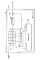
- FIG. 1 is a block diagram showing a schematic configuration of the photoelectric conversion apparatus according to the present embodiment.
- a photoelectric conversion device 1 includes pixels P11 to P45, a vertical scanning circuit 4, CDS circuits 51 to 55 (hereinafter referred to as CDS51 to CDS55), a horizontal scanning circuit 6, a control circuit 7, and AD converters 81 to 85 ( Hereinafter, it is referred to as ADC81 to ADC85).
- the pixels P11 to P45 are arranged two-dimensionally in 4 rows and 5 columns and configured as a pixel array 3.
- the CDS 51 to CDS 55 are collectively referred to as “CDS 5”.
- the ADCs 81 to 85 are collectively shown, they are referred to as “ADC8”.
- Pixels P11 to P45 are photoelectric conversion elements.
- the pixels P11 to P45 output a pixel output signal at a level corresponding to the amount of incident light when the own pixel 2 is selected by the vertical scanning circuit 4.
- the pixels P11 to P45 are two-dimensionally arranged in 4 rows and 5 columns as the pixel array 3 and output pixel output signals ⁇ P1 to ⁇ P5 for each pixel column.
- the first number following the pixel P indicated by the pixels P11 to P45 represents the row number, and the last numerical value represents the column number.
- CDS51 to CDS55 are arranged in each pixel column of the pixel array 3, and the difference between the pixel output signal read from the pixel 2 and the pixel reset signal is obtained as a pixel signal ⁇ C1 to ⁇ C1 corresponding to the image data exposed by the pixel 2.
- the numbers following CDS 5 indicated by CDS 51 to CDS 55 indicate the column numbers of the pixel array 3.
- ADC81 to ADC85 are AD converters that perform analog / digital conversion on the pixel signals ⁇ C1 to ⁇ C5 input from the CDS51 to CDS55.
- the ADCs 81 to 85 perform analog / digital conversion on the input pixel signal and output the converted digital value.
- the numbers following ADC 8 indicated by ADC 81 to ADC 85 indicate the column numbers of the pixel array 3.
- the vertical scanning circuit 4 is a circuit that selects a row of pixels 2 to be read from the pixel array 3 in accordance with a vertical control signal input from the control circuit 7.
- the vertical scanning circuit 4 outputs row selection signals ⁇ SL1 to ⁇ SL4 corresponding to the rows of the pixels 2 read from the pixel array 3. For example, when the vertical scanning circuit 4 selects the first row of the pixel array 3, a selection level (for example, “High” level) is output to the pixel array 3 as the row selection signal ⁇ SL1, and other unselected rows A non-selection level (for example, “Low” level) is output to the pixel array 3 as the selection signals ⁇ SL2 to ⁇ SL4.
- a selection level for example, “High” level
- a non-selection level for example, “Low” level
- the horizontal scanning circuit 6 is a circuit that outputs the digital value analog-digital converted by the ADC 81 to ADC 85 for each column in accordance with the horizontal control signal input from the control circuit 7 and outputs it to the photoelectric conversion device.
- the horizontal scanning circuit 6 outputs column selection signals ⁇ H1 to ⁇ H5 corresponding to the columns of digital values read from the ADC 8 to the ADC 8. For example, when the horizontal scanning circuit 6 outputs the digital value of the first column of the pixel array 3, the column selection signal ⁇ H1 is set to the output permission level (for example, “High” level) and output to the ADC 8 and others are output.
- Unselected column selection signals ⁇ H2 to ⁇ H5 are set to an output non-permitted level (eg, “Low” level) and output to the ADC 8. Subsequently, the column selection signals ⁇ H2 to ⁇ H5 are sequentially output permission level (for example, “High” level), and the column selection signals ⁇ H1 to ⁇ H5 corresponding to the other columns not to be output are output non-permission levels (for example “Low” level). At the same time), the digital value converted by the ADC 8 is sequentially output to the ADC 8.
- an output non-permitted level eg, “Low” level
- the column selection signals ⁇ H2 to ⁇ H5 are sequentially output permission level (for example, “High” level)
- the column selection signals ⁇ H1 to ⁇ H5 corresponding to the other columns not to be output are output non-permission levels (for example “Low” level).
- the digital value converted by the ADC 8 is sequentially output to the ADC 8.
- the control circuit 7 is a circuit that controls the entire photoelectric conversion device.
- the control circuit 7 outputs a vertical control signal for controlling the vertical scanning circuit 4 and a horizontal control signal for controlling the horizontal scanning circuit 6 in response to an external image capture command (not shown).
- the control circuit 7 controls the operations (operation start and operation stop) of the CDS 5 and the ADC 8.
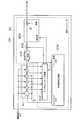
- FIG. 2 is a block diagram showing a schematic configuration according to the first embodiment of one AD converter (ADC 81) of the AD converters included in the photoelectric conversion apparatus 1 according to the present embodiment.
- the other ADCs 82 to 85 are the same as the ADC 81 shown in FIG.
- the ADC 81 includes a delay circuit 811 and a correction encoder 812.
- the correction encoder 812 includes a counter circuit 8121, a latch & encoder circuit 8122, an adder 8123, and a control signal generator 8124.
- the ADC 81 performs analog / digital conversion of the pixel signal ⁇ C1 input from the CDS 51 in accordance with an analog / digital conversion start timing signal (not shown). Further, it is held in an output control circuit in the ADC 81 (not shown) in response to a timing signal for completion of analog / digital conversion not shown, and held in an output control circuit (not shown) in response to a column selection signal ⁇ H1 input from the horizontal scanning circuit 6. Output digital value.
- the delay circuit 811 is a ring delay line (RDL) in which a plurality of gate circuits (hereinafter referred to as delay units) having a delay amount corresponding to the power supply voltage are connected in a ring shape and circulates the input pulse ⁇ PL.
- RDL ring delay line
- delay units a plurality of gate circuits having a delay amount corresponding to the power supply voltage
- the input pulse ⁇ PL is applied to one input terminal of the first-stage NAND gate. Is input to the other input terminal, and the output of the final NOT gate is logically inverted whenever the delay circuit 811 is operating.
- the NOT gates in the second and subsequent stages logically invert the value input to the input terminal and output it to the output terminal.
- An input signal that is, a pixel signal ⁇ C1 input from the CDS 51 to be subjected to analog / digital conversion is applied to the delay unit of the delay circuit 811.
- Each delay unit is input from the preceding delay unit.
- the input pulse ⁇ PL is output to the delay unit of the next stage with a delay time corresponding to the level difference between the voltage level of the power supply voltage (pixel signal ⁇ C1) and the reference voltage (ground: GND level in FIG. 2).
- Each delay unit connected in a ring shape operates in the same manner, and the input pulse ⁇ PL is sequentially transmitted from the preceding stage to the subsequent delay unit, so that the input pulse ⁇ PL circulates in the delay circuit 811.
- the correction encoder 812 is a circuit that detects the number of stages where the input pulse ⁇ PL has passed through the delay unit in the delay circuit 811 and outputs the number of stages as a digital value that is the result of analog-digital conversion by the ADC 81. Further, the correction encoder 812 has a period in which the circulation time of the input pulse ⁇ PL that circulates in the delay circuit 811 after the operation of the ADC 81 is unstable (hereinafter, a period in which the circulation time of the input pulse ⁇ PL that circulates in the delay circuit 811 does not stabilize). Initialize the unstable digital value that is output during the “pulse instability period”).
- the result of analog / digital conversion during the pulse instability period is invalidated, and the digital value of the analog / digital conversion result output from the ADC 81 is corrected.
- the digital value output from the correction encoder 812 is held in an output control circuit in the ADC 81 (not shown) in accordance with an analog / digital conversion completion timing signal (not shown).
- the counter circuit 8121 is a circuit that detects the number of times that the input pulse ⁇ PL has circulated around the delay circuit 811 and outputs the detected number of times (count value). The counter circuit 8121 adds 1 to the count value every time the input pulse ⁇ PL passes through the final stage of the delay circuit 811 and outputs the count value. In addition, the counter circuit 8121 temporarily stores, for example, the number of times the input pulse ⁇ PL circulated around the delay circuit 811 at the rising timing of the reset signal ⁇ RS, and then the input level of the reset signal ⁇ RS (for example, “High” level) If it is held for a predetermined period, the number of laps in which the temporarily stored input pulse ⁇ PL circulates the delay circuit 811 is initialized.
- the latch & encoder circuit 8122 is a circuit that detects the number of stages in which the input pulse ⁇ PL has passed through the delay unit in the delay circuit 811 and outputs the detected number of passing stages.
- the latch & encoder circuit 8122 temporarily stores, for example, the value of each delay unit in the delay circuit 811 in which the input pulse ⁇ PL circulates at the rising timing of the reset signal ⁇ RS, and each delay in the delay circuit 811 temporarily stored. Outputs the unit value.
- the adder 8123 processes the number of laps input from the counter circuit 8121 and the number of passing stages input from the latch & encoder circuit 8122, and inputs the input signal, that is, input from the CDS 51 to be subjected to analog / digital conversion. This circuit outputs a digital value corresponding to the pixel signal ⁇ C1 as a result of analog-digital conversion by the ADC 81.
- the adder 8123 processes the number of turns input from the counter circuit 8121 as the upper bits of the digital value output from the ADC 81 and the number of passing stages input from the latch & encoder circuit 8122 as the lower bits of the digital value output from the ADC 81. .
- the control signal generation unit 8124 is a circuit that generates a control signal to be input to the delay circuit 811, the counter circuit 8121, and the latch & encoder circuit 8122 in order to correct the digital value output from the ADC 81.
- an analog / digital conversion start timing signal (not shown) enters an analog / digital conversion start state
- the control signal generator 8124 sets the input pulse ⁇ PL that circulates in the delay circuit 811 to the “High” level and is input from the CDS 51.
- the circuit circulates in the delay circuit 811 with a delay time corresponding to the pixel signal ⁇ C1.
- control signal generation unit 8124 sets the input pulse ⁇ PL that circulates in the delay circuit 811 to the “Low” level, and delay circuit 811. Stop laps inside.
- control signal generation unit 8124 outputs a reset signal ⁇ RS (for example, a pulse that becomes “High” level for a predetermined period) for initializing (invalidating) the counter circuit 8121 during the pulse instability period.
- a reset signal ⁇ RS for example, a pulse that becomes “High” level for a predetermined period
- the rising timing of the reset signal ⁇ RS output from the control signal generation unit 8124 is a timing for temporarily storing the number of times that the input pulse ⁇ PL by the counter circuit 8121 circulates the delay circuit 811 when the analog / digital conversion period ends. It is also used as a timing signal for temporarily storing the signal and the value of each delay unit in the delay circuit 811 in which the input pulse ⁇ PL by the latch & encoder circuit 8122 circulates.
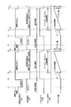
- FIG. 3 is a timing chart showing an outline of the operation of the photoelectric conversion apparatus 1 according to the present embodiment.
- the ADC 81 acquires digital values of the pixels P11 and P21 in the first column of the pixel array 3 that performs analog-digital conversion will be described.
- the other ADCs 82 to 85 are similar in timing to the ADC 81 shown in FIG.
- the photoelectric conversion device 1 is initialized from the outside (not shown), the pixel output signal ⁇ P1 has a voltage level in a reset state of the pixel P11, and the pixel signal ⁇ C1 has a voltage level indicating no output. Further, the input pulse ⁇ PL and the reset signal ⁇ RS are initial values (“Low” level), and the counter value is “0”. Thereafter, when an image capture command is input from outside (not shown), the pixel array 3 performs exposure.
- the control circuit 7 outputs a vertical control signal for selecting the pixel P11 to the vertical scanning circuit 4, and the pixel P11 selected by the row selection signal ⁇ SL1 input from the vertical scanning circuit 4
- the pixel output signal ⁇ P1 corresponding to the amount of incident light is output. Since the input pulse ⁇ PL is at the “Low” level, the delay circuit 811 is in a non-operating (standby) state.
- the CDS 51 outputs the pixel signal ⁇ C1 to the ADC 81 in accordance with the pixel output signal ⁇ P1 input from the pixel P11 and the pixel reset signal.
- the control signal generation unit 8124 sets the input pulse ⁇ PL that circulates in the delay circuit 811 to the “High” level, the voltage level of the pixel signal ⁇ C1 input from the CDS 51 and the reference voltage (for example, the ground in FIG. 2)
- the input pulse ⁇ PL circulates in the delay circuit 811 with a delay time corresponding to the level difference from the GND level).
- the counter circuit 8121 and the latch & encoder circuit 8122 start detecting each delay unit in the delay circuit 811. Note that the detection result of the delay unit starting from the timing t2 is a pulse unstable period.
- control signal generation unit 8124 sets the reset signal ⁇ RS to “High” level and initializes (invalidates) the detection result of the counter circuit 8121.
- the control signal generation unit 8124 sets the reset signal ⁇ RS to the “Low” level, and the counter circuit 8121 and the latch & encoder circuit 8122. Cancel initialization of detection results. As a result, the counter circuit 8121 and the latch & encoder circuit 8122 resume detection of each delay unit in the delay circuit 811.
- the circulation in the delay circuit 811 continues.
- the input pulse ⁇ PL continues to circulate in the delay circuit 811 until the timing t4, so that the circulation time of the input pulse ⁇ PL is stabilized.
- the counter circuit 8121 and the latch & encoder circuit 8122 can detect a period in which the circulation time of the input pulse ⁇ PL is stable, and can correct the digital value output from the ADC 81.
- the control signal generation unit 8124 sets the input pulse ⁇ PL to the “Low” level
- the circulation of the input pulse ⁇ PL in the delay circuit 811 stops.
- the control signal generation unit 8124 sets the reset signal ⁇ RS to the “High” level.
- the adder 8123 processes the temporarily stored number of laps and the number of passage stages, and outputs a digital value corresponding to the incident light amount of the pixel P11.
- the output digital value is held in an output control circuit in the ADC 81 (not shown). Thereafter, when the ADC 81 is selected by the column selection signal ⁇ H1 input from the horizontal scanning circuit 6, a digital value held in an output control circuit (not shown) in the ADC 81, that is, a digital value corresponding to the incident light amount of the pixel P11 is obtained. Output as a result of analog-digital conversion.
- the analog / digital conversion result for the pixel P11 is initialized at the timing of t6.
- the control circuit 7 outputs a vertical control signal for selecting the pixel P21 to the vertical scanning circuit 4, and the pixel P21 selected by the row selection signal ⁇ SL2 input from the vertical scanning circuit 4
- the pixel output signal ⁇ P1 corresponding to the amount of incident light is output.
- the ADC 81 performs analog-digital conversion on the pixel P21.
- the pixel P21 is selected.
- the digital value corresponding to the incident light quantity is output as a result of analog-digital conversion.
- the ADC 81 outputs the digital value corresponding to the incident light amount of the pixel P31 and the pixel P41 as a result of analog-digital conversion, and performs analog-digital conversion of the pixel array 3 in the same manner as the timings t1 to t6 described above. That is, reading of all image signals of the photoelectric conversion device 1 is completed.
- the AD converter in a low power consumption AD converter (for example, adapted to signal processing of an imager) mounted on a battery or a digital camera or a digital video camera operated by the battery, the AD converter is operated from a non-operating state.
- the effect of digital value correction according to the present invention is high, and a good digital value in which noise of the obtained output signal is reduced can be obtained.
- the example in which the ADCs 81 to 85 are arranged according to the amount of incident light of the pixel array 3 arranged in two dimensions in four rows and five columns has been described.
- a linear sensor in which a plurality of pixels are arranged in one column. It is also possible to apply to an AD converter that performs analog / digital conversion of the output of.
- the CDS 5 may not be disposed, and corresponds to the difference between the pixel reset signal of the pixel output signal and the optical signal. If the pixel signal to be input is input to the ADC 8, analog / digital conversion can be performed in the same manner.
- the example in which the reset signal ⁇ RS is maintained at the “Low” level, which is the initial value, from the timing t2 to the timing t3 has been described. It is also possible to set the “High” level until the timing of t 3, that is, the period from the timing of t 2 to the timing of t 4 as the reset period of the counter circuit 8121. Accordingly, the operation of the counter circuit 8121 during the period from the timing t2 to the timing t3 in the present embodiment can be stopped, and the power consumption of the photoelectric conversion device 1 can be further reduced.
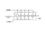
- FIG. 4 is a block diagram showing a schematic configuration of an AD converter (ADC 810) according to the second embodiment.
- the ADC 810 includes a delay circuit 811 and a correction encoder 813.
- the correction encoder 813 includes a counter circuit 8121, a latch & encoder circuit 8122, an adder 8123, a control signal generation unit 8134, and a correction unit 8135.
- the ADC 810 is an AD converter that replaces the ADC 81 illustrated in the photoelectric conversion device 1 of FIG. 1.
- a correction unit 8135 is added to the subsequent stage of the adder 8123 with respect to the ADC 81 illustrated in FIG. Is changed to a control signal generation unit 8134.
- the control signal generation unit 8134 differs from the control signal generation unit 8124 illustrated in FIG. 2 in the timing of the reset signal ⁇ RS to be output.
- the ADC 810 performs analog / digital conversion of the pixel signal ⁇ C1 input from the CDS 51 in accordance with an analog / digital conversion start timing signal (not shown) in the same manner as the ADC 81 of the first embodiment shown in FIG. Further, the ADC 810 holds the result of analog / digital conversion in an output control circuit in the ADC 810 (not shown) in accordance with a timing signal of completion of analog / digital conversion (not shown), and a column selection signal ⁇ H1 input from the horizontal scanning circuit 6. In response to this, a digital value held in an output control circuit (not shown) is output.
- the delay circuit 811 of the ADC 810, the counter circuit 8121 of the correction encoder 813, the latch & encoder circuit 8122, and the adder 8123 perform the same operations as the corresponding blocks of the ADC 81 of the first embodiment shown in FIG. .
- the control signal generation unit 8134 is a circuit that generates control signals to be input to the delay circuit 811, the counter circuit 8121, the latch & encoder circuit 8122, and the correction unit 8135 in order to correct the digital value output from the ADC 810. is there.
- the input pulse ⁇ PL generated by the control signal generation unit 8134 for the delay circuit 811 is the same as that of the control signal generation unit 8124 shown in FIG.
- the control signal generation unit 8134 also resets the counter signal 8RS (for example, a predetermined signal) for initializing the counter circuit 8121 at the timing when the analog / digital conversion is started by the ADC 810 and when the analog / digital conversion is completed. During the period "High" level). Also, the rising timing of the reset signal ⁇ RS output from the control signal generator 8134 is the timing for temporarily storing the number of times that the input pulse ⁇ PL by the counter circuit 8121 circulates the delay circuit 811 when the analog / digital conversion period ends. It is also used as a timing signal for temporarily storing the signal and the value of each delay unit in the delay circuit 811 in which the input pulse ⁇ PL by the latch & encoder circuit 8122 circulates.
- the counter signal 8RS for example, a predetermined signal
- the correction unit 8135 subtracts a predetermined digital value from the digital value output from the adder 8123, and corresponds to the input signal, that is, the pixel signal ⁇ C1 input from the CDS 51 to be subjected to analog-digital conversion. This is a circuit that outputs a digital value as a result of analog-digital conversion by the ADC 810.
- the correction unit 8135 is configured by the arithmetic circuit 35.
- the arithmetic circuit 35 is an arithmetic circuit that subtracts a predetermined constant digital value corresponding to the unstable digital value output during the pulse instability period from the digital value input from the adder 8123.
- a predetermined digital value that is subtracted from the digital value output from the adder 8123 and a method for setting the digital value are not defined.
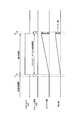
- FIG. 5 is a timing chart showing an outline of an analog / digital conversion operation in the AD converter according to the second embodiment.
- the ADC 810 disposed at the position of the ADC 81 performs analog / digital conversion of the pixel P11 in the first column of the pixel array 3 in the photoelectric conversion device 1 illustrated in FIG. 1 will be described.
- the drive timing of the ADC 810 is different from the drive timing of the ADC 81 shown in FIG. 3 in the timing of the reset signal ⁇ RS. Further, the timing of the AD converter corresponding to the pixel output signal ⁇ P1 corresponding to the amount of incident light of the pixels P21, P31, and P41 in the first column of the other pixel array 3 and the ADCs 82 to 85 is shown in FIG. The timing is the same as that. The timing of the pixel output signal ⁇ P1 output from the pixel array 3 and the pixel signal ⁇ C1 output from the CDS5 are the same as the timing shown in FIG.
- the control signal generation unit 8134 sets the input pulse ⁇ PL that circulates in the delay circuit 811 to the “High” level at the timing t2, the voltage level of the pixel signal ⁇ C1 input from the CDS 51 and the reference voltage (for example, 4, the input pulse ⁇ PL circulates in the delay circuit 811 with a delay time corresponding to the level difference from the ground (GND level in FIG. 4). Further, the control signal generation unit 8134 sets the reset signal ⁇ RS to the “Low” level at the timing t 2, whereby the counter circuit 8121 and the latch & encoder circuit 8122 start detecting each delay unit in the delay circuit 811. . Note that the detection result of the delay unit starting from the timing t2 includes a pulse instability period.
- the control signal generation unit 8134 sets the reset signal ⁇ RS to the “High” level.
- the adder 8123 processes the temporarily stored number of laps and the number of passage stages, and outputs a digital value corresponding to the incident light amount of the pixel P11 to the correction unit 8135.
- the correction unit 8135 calculates a predetermined digital value corresponding to the unstable digital value output during the pulse unstable period from the digital value corresponding to the incident light amount of the pixel P11 output from the adder 8123. Subtract and output the resulting digital value (corrected digital value).
- the digital value output from the correction unit 8135 is held in an output control circuit in the ADC 810 (not shown). Thereafter, when the ADC 810 is selected by the column selection signal ⁇ H1 input from the horizontal scanning circuit 6, a digital value held in an output control circuit (not shown) in the ADC 810, that is, a digital value corresponding to the incident light amount of the pixel P11 is obtained. Output as a result of analog-digital conversion.
- control signal generation unit 8134 sets the reset signal ⁇ RS to the “Low” level at timing t4, whereby the analog / digital conversion of the pixel output signal ⁇ P1 corresponding to the incident light amount of the pixel P11 is completed.
- the ADC 810 outputs a digital value corresponding to the incident light amount of the pixel P21, the pixel P31, and the pixel P41 as an analog-digital conversion result, and outputs the analog value of the pixel array 3. Digital conversion, that is, reading of all image signals of the photoelectric conversion device 1 is completed.
- the unstable digital value output in the pulse unstable period is obtained. Since correction (subtraction) can be performed, good image data (digital value after correction) with reduced noise appearing in the output image can be obtained.
- FIG. 6 is a block diagram showing a schematic configuration of an AD converter (ADC 820) according to the third embodiment.
- the ADC 820 includes a delay circuit 811 and a correction encoder 814.
- the correction encoder 814 includes a counter circuit 8121, a latch & encoder circuit 8122, an adder 8123, a control signal generation unit 8134, and a correction unit 8145.
- the ADC 820 is an AD converter that replaces the ADC 81 illustrated in the photoelectric conversion device 1 in FIG. 1, and the correction unit 8135 of the ADC 810 illustrated in FIG. 4 is changed to a correction unit 8145.
- the correction unit 8145 has a different internal configuration from the correction unit 8135 shown in FIG.
- the ADC 820 performs analog / digital conversion of the pixel signal ⁇ C1 input from the CDS 51 in accordance with an analog / digital conversion start timing signal (not shown) in the same manner as the ADC 81 of the first embodiment shown in FIG.
- the ADC 820 holds the result of analog-digital conversion in an output control circuit in the ADC 820 (not shown) in accordance with an analog / digital conversion completion timing signal (not shown), and a column selection signal ⁇ H1 input from the horizontal scanning circuit 6. In response to this, a digital value held in an output control circuit (not shown) is output.
- the delay circuit 811 of the ADC 820, the counter circuit 8121 of the correction encoder 814, the latch & encoder circuit 8122, and the adder 8123 are the ADC 81 of the first embodiment shown in FIG. 2, and the second circuit shown in FIG. The same operation as the corresponding block of the ADC 810 of the embodiment is performed. Further, the control signal generation unit 8134 of the correction encoder 814 performs the same operation as the corresponding block of the ADC 810 of the second embodiment illustrated in FIG.
- the correction unit 8145 calculates a correction coefficient corresponding to the digital value output from the adder 8123, and subtracts a correction value (digital value) corresponding to the calculated correction coefficient from the digital value output from the adder 8123.
- the ADC 820 outputs a digital value corresponding to the pixel signal ⁇ C1 input from the CDS 51 to be subjected to analog / digital conversion as a result of analog / digital conversion.
- the correction unit 8145 includes an arithmetic circuit 45 and a correction coefficient calculation unit 451.
- the correction coefficient calculation unit 451 calculates a predetermined ratio of correction coefficients from the digital value input from the adder 8123 according to the pulse instability period, and calculates a correction value (digital value) according to the calculated correction coefficient. ).
- the correction coefficient calculation unit 451 outputs the generated correction value (digital value) to the arithmetic circuit 45.
- the temperature characteristic of the photoelectric conversion device 1 with respect to the ambient temperature in which the photoelectric conversion device 1 of FIG. A change in the output digital value is measured in advance and the correction ratio in the environmental temperature difference can be used as a correction coefficient.
- the temperature characteristics of the photoelectric conversion device 1 are such that when the environmental temperature increases by 10 degrees, the digital value output from the adder 8123 becomes 10% larger.
- the environmental temperature of the photoelectric conversion device 1 is 20 degrees higher. From the measured environmental temperature and the temperature characteristic, it is calculated that the digital value output from the adder 8123 is 20% larger.
- the correction coefficient calculation unit 451 uses the calculated value of 20% as the correction coefficient. Further, using the calculated correction coefficient of 20%, a value corresponding to the correction coefficient (20%) of the digital value output from the adder 8123 is calculated and used as a correction value. As a result, the influence of the environmental temperature of the digital value output by the photoelectric conversion device 1 can be reduced. In the present invention, there are no rules regarding the correction coefficient setting method and calculation method.
- the arithmetic circuit 45 is an arithmetic circuit that subtracts the correction value (digital value) input from the correction coefficient calculation unit 451 from the digital value input from the adder 8123.
- the analog / digital conversion timing in the AD converter according to the third embodiment is the same as the analog / digital conversion timing in the AD converter according to the second embodiment shown in FIG.
- the correction of the digital value corresponding to the incident light amount of the pixel P11 output from the adder 8123 performed at the timing t3 is performed by the correction coefficient calculation unit 451 from the digital value input from the adder 8123 to the pulse unstable period. Accordingly, a digital value (corrected digital value) calculated based on a predetermined fixed correction coefficient is obtained.
- the unstable digital value output in the pulse unstable period is obtained. Since correction can be performed using the correction coefficient, it is possible to obtain good image data (digital value after correction) with reduced noise appearing in the output image.
- FIG. 7 is a block diagram showing a schematic configuration of an AD converter (ADC 830) according to the fourth embodiment.
- the ADC 830 includes a delay circuit 811 and a correction encoder 815.
- the correction encoder 815 includes a counter circuit 8121, a latch & encoder circuit 8122, an adder 8123, a control signal generation unit 8154, and a correction unit 8155.
- the ADC 830 is an AD converter that replaces the ADC 81 shown in the photoelectric conversion device 1 in FIG. 1.
- the control signal generation unit 8134 of the ADC 810 shown in FIG. 4 is replaced with the control signal generation unit 8154, and the correction unit 8135 is replaced with the correction unit 8155. Each has been changed.
- the ADC 830 performs analog / digital conversion of the pixel signal ⁇ C1 input from the CDS 51 in accordance with an analog / digital conversion start timing signal (not shown), similarly to the ADC 81 of the first embodiment shown in FIG.
- the ADC 830 holds the result of analog-digital conversion in an output control circuit in the ADC 830 (not shown) in accordance with an analog-digital conversion completion timing signal (not shown), and the column selection signal ⁇ H1 input from the horizontal scanning circuit 6 In response to this, a digital value held in an output control circuit (not shown) is output.
- the delay circuit 811 of the ADC 830, the counter circuit 8121 of the correction encoder 815, the latch & encoder circuit 8122, and the adder 8123 are the ADC 81 of the first embodiment shown in FIG. 2, and the second embodiment shown in FIG.
- the same operation as that of the corresponding block of the ADC 810 of the embodiment and the ADC 820 of the third embodiment shown in FIG. 6 is performed.
- the input pulse ⁇ PL generated by the control signal generation unit 8154 of the correction encoder 815 and the reset signal ⁇ RS correspond to the ADC 810 of the second embodiment shown in FIG. 4 and the ADC 820 of the third embodiment shown in FIG.
- a latch control signal ⁇ LC1 and a latch control signal ⁇ LC2 for controlling the correction unit 8155 are newly added, although the same as the block to be performed.
- the correction unit 8155 temporarily stores the digital value output from the adder 8123 and performs correction based on the temporarily stored digital value, thereby inputting from the input signal, that is, the CDS 51 that is the target of analog-digital conversion. This is a circuit for outputting a digital value corresponding to the pixel signal ⁇ C1 as a result of analog-digital conversion by the ADC 830.
- the correction unit 8155 includes a first latch circuit 551, a second latch circuit 552, and an arithmetic circuit 55.
- the first latch circuit 551 temporarily stores the digital value input from the adder 8123 in accordance with the latch control signal ⁇ LC1 input from the control signal generation unit 8154 (for example, at the rising timing of the latch control signal ⁇ LC1). Circuit.
- the second latch circuit 552 temporarily stores the digital value input from the adder 8123 according to the latch control signal ⁇ LC2 input from the control signal generator 8154 (for example, at the falling timing of the latch control signal ⁇ LC2). Circuit.
- the arithmetic circuit 55 is an arithmetic circuit that subtracts the digital value temporarily stored in the first latch circuit 551 from the digital value temporarily stored in the second latch circuit 552.
- the control signal generation unit 8154 is a circuit that generates control signals to be input to the delay circuit 811, the counter circuit 8121, the latch & encoder circuit 8122, and the correction unit 8155 in order to correct the digital value output from the ADC 830. is there.
- the input pulse ⁇ PL and the reset signal ⁇ RS generated by the control signal generation unit 8154 for the delay circuit 811 are the same as those of the control signal generation unit 8134 shown in FIGS.
- the control signal generator 8154 also has a latch control signal ⁇ LC1 (for example, a predetermined value) for temporarily storing the digital value input from the adder 8123 to the first latch circuit 551 at the timing when the pulse instability period ends. During this period, a pulse having a “High” level) is output.
- the control signal generation unit 8154 has a latch control signal ⁇ LC2 (for example, a predetermined value) for temporarily storing the digital value input from the adder 8123 to the second latch circuit 552 at the timing when the analog / digital conversion period ends. For a given period, a pulse having a “High” level) is output.
- an unstable digital value output in a predetermined period that is, a pulse unstable period is temporarily stored in the first latch circuit 551, and an analog including a pulse unstable period is stored.
- the digital value of the entire digital conversion period can be temporarily stored in the second latch circuit 552.
- the first latch circuit Thereafter, from the digital value temporarily stored in the second latch circuit 552 by the arithmetic circuit 55 of the correction unit 8155, that is, the digital value of the entire analog-digital conversion period including the pulse unstable period, the first latch circuit
- the digital value temporarily stored in 551, that is, the unstable digital value output during the pulse unstable period can be subtracted, and the resulting digital value (digital value after correction) can be obtained.
- the digital value output from the correction unit 8155 is held in an output control circuit in the ADC 830 (not shown). Thereafter, when the ADC 830 is selected by the column selection signal ⁇ H1 input from the horizontal scanning circuit 6, a digital value held in an output control circuit in the ADC 830 (not shown), that is, a digital value corresponding to the incident light amount of the pixel P11 is obtained. Output as a result of analog-digital conversion.
- FIG. 8 is a timing chart showing an outline of an analog / digital conversion operation in the AD converter according to the fourth embodiment.
- the ADC 830 arranged at the position of the ADC 81 performs analog / digital conversion of the pixel P11 in the first column of the pixel array 3 in the photoelectric conversion device 1 illustrated in FIG. 1 will be described.
- the drive timing of the ADC 830 is the same as the drive timing of the ADC 81 shown in FIG. 5, but the output timing of the latch control signal ⁇ LC1 and the latch control signal ⁇ LC2 for controlling the correction unit 8155 is newly added. Yes. Further, the timing of the AD converter corresponding to the pixel output signal ⁇ P1 corresponding to the amount of incident light of the pixels P21, P31, and P41 in the first column of the other pixel array 3 and the ADCs 82 to 85 is shown in FIG. The timing is the same as that. The timing of the pixel output signal ⁇ P1 output from the pixel array 3 and the pixel signal ⁇ C1 output from the CDS5 are the same as the timing shown in FIG.
- the control signal generation unit 8154 sets the input pulse ⁇ PL that circulates in the delay circuit 811 to the “High” level, thereby inputting from the CDS 51.
- the input pulse ⁇ PL circulates in the delay circuit 811 with a delay time corresponding to the level difference between the voltage level of the pixel signal ⁇ C1 and the reference voltage (for example, ground: GND level in FIG. 7), and control
- the signal generation unit 8154 sets the reset signal ⁇ RS to the “Low” level
- the counter circuit 8121 and the latch & encoder circuit 8122 start detecting each delay unit in the delay circuit 811. Note that the detection result of the delay unit starting from the timing t2 includes a pulse instability period, as in the timing chart shown in FIG.
- the control signal generation unit 8154 outputs the latch control signal ⁇ LC1 (for example, “High” pulse) of the first latch circuit 551.
- the first latch circuit 551 temporarily stores the digital value input from the adder 8123 during the pulse unstable period, that is, the unstable digital value output during the pulse unstable period.
- the control signal generation unit 8154 outputs the latch control signal ⁇ LC2 (for example, “High” pulse) of the second latch circuit 552 at the timing of t4.
- the latch control signal ⁇ LC2 the second latch circuit 552 temporarily stores the digital value of the entire analog / digital conversion period including the pulse instability period.
- the arithmetic circuit 55 outputs the digital value of the entire analog / digital conversion period temporarily stored in the second latch circuit 552 during the pulse unstable period temporarily stored in the first latch circuit 551.
- the unstable digital value is subtracted, and the resulting digital value (corrected digital value) is output.
- the control signal generation unit 8154 sets the input pulse ⁇ PL to the “Low” level to input
- the circulation of the pulse ⁇ PL in the delay circuit 811 stops, and the control signal generation unit 8154 sets the reset signal ⁇ RS to “High” level, so that the digital value (corrected digital value) calculated by the arithmetic circuit 55 is obtained.
- Held in an output control circuit in the ADC 830 (not shown).
- the control signal generation unit 8154 sets the reset signal ⁇ RS to the “Low” level, whereby the analog / digital conversion of the pixel output signal ⁇ P1 corresponding to the incident light amount of the pixel P11 is completed.
- a digital value (corrected digital value) calculated by the arithmetic circuit 55 held in the output control circuit in the ADC 830 (not shown) is selected by the ADC 830 by the column selection signal ⁇ H1 input from the horizontal scanning circuit 6, It is read from an output control circuit in the ADC 830 (not shown) and output as a result of analog-digital conversion of a digital value corresponding to the amount of incident light of the pixel P11.
- the ADC 830 outputs the digital value corresponding to the incident light amount of the pixel P21, the pixel P31, and the pixel P41 as an analog-to-digital conversion result and outputs the analog value of the pixel array 3 in the same manner as the timings t1 to t6 described above.
- Digital conversion that is, reading of all image signals of the photoelectric conversion device 1 is completed.
- the unstable digital value output in the pulse unstable period is obtained. Since correction (subtraction) can be performed, good image data (digital value after correction) with reduced noise appearing in the output image can be obtained.
- the correction unit 8155 in the fourth embodiment has the first latch circuit 551 and the second latch circuit 552, it includes only the first latch circuit 551 and is input from the adder 8123.
- the unstable digital value output during the pulse instability period temporarily stored in the first latch circuit 551 is subtracted from the obtained digital value, and the resulting digital value (corrected digital value) is output. It can also be.
- the input pulse ⁇ PL detected by the counter circuit 8121 at the rising timing of the reset signal ⁇ RS controlled by the control signal generator 8154 at the timing t5 shown in FIG. 8 in the same manner as the timing t3 shown in FIG.
- the adder 8123 processes it.
- the digital value by the arithmetic circuit 55 can be corrected (subtracted).
- the digital value output after the start of the operation of the AD converter included in the photoelectric conversion device is corrected during the unstable period. Therefore, a good digital value in which noise included in the digital value in an unstable period is reduced can be obtained.
- the photoelectric conversion device of the present invention is mounted on a digital camera, a digital video camera or the like that operates with a battery or battery, the operation of the AD converter provided in the photoelectric conversion device can be actively stopped. The power consumption of the digital camera, digital video camera, etc. can be reduced.
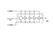
- the delay unit in the delay circuit 811 of the present embodiment has been described with a configuration in which the power supply side is the input signal, that is, the pixel signal ⁇ C1 to be subjected to analog / digital conversion, and the ground side is the reference voltage.
- the power supply side may be a reference voltage and the ground side may be an input signal. If there are two types of input signals, the power supply side can be the first input signal and the ground side can be the second input signal as shown in the delay circuit 851 of FIG. Further, in contrast to the delay circuit 851 in FIG. 10, the power supply side may be the second input signal and the ground side may be the first input signal.
- the delay circuit of the present embodiment the case where the first delay unit is configured by a NAND circuit (NAND gate) and the other delay units are configured by a NOT circuit (NOT gate) has been described. Does not define the configuration of the delay circuit.
- the delay circuit can be configured in any configuration as long as it circulates the input pulse with a delay time corresponding to the voltage level of the input signal and the voltage level of the reference voltage, or the level difference between the two input signal voltage levels. It can be applied even if it exists.
- a good digital value can be obtained by analog / digital conversion of a pixel signal corresponding to the amount of incident light of the photoelectric conversion element.
- Photoelectric conversion device 2 P11, P12, P13, P14, P15, P21, P22, P23, P24, P25, P31, P32, P33, P34, P35, P41, P42, P43, P44, P45 Pixel 3 Pixel array 4 Vertical scanning circuit 5, 51, 52, 53, 54, 55 CDS circuit 6 Horizontal scanning circuit 7 Control circuit 8, 81, 82, 83, 84, 85, 810, 820, 830 AD converters 811, 841, 851 Delay circuit 812, 813, 814, 815 Correction encoder 8121 Counter circuit 8122 Latch & encoder circuit 8123 Adder 8124, 8134, 8154 Control signal generation unit 8135, 8145, 8155 Correction unit 35, 45, 55 Calculation circuit 451 Correction coefficient calculation unit 551 1st 1 latch circuit 552 second Latch circuit 90 Pixel block 91 AD converter B1, B2, B3, B4, B5, B6, B7, B8, B9, B10, B11, B12, B13, B14,
Landscapes
- Engineering & Computer Science (AREA)
- Multimedia (AREA)
- Signal Processing (AREA)
- Theoretical Computer Science (AREA)
- Transforming Light Signals Into Electric Signals (AREA)
- Solid State Image Pick-Up Elements (AREA)
Abstract
光電変換装置は、画素アレイと、複数のAD変換器と、を有する。前記画素アレイは、光電変換素子を有し、該光電変換素子への入射光量に応じた画素信号を出力する画素が二次元に複数配置されている。前記複数のAD変換器は、前記画素アレイから読み出した前記画素信号をデジタル値に変換して出力する。前記AD変換器は、パルス遅延回路と、エンコーダ部と、補正手段と、を有する。前記パルス遅延回路では、前記画素アレイから読み出した前記画素信号の電圧の大きさに応じた遅延時間でパルス信号を遅延させる遅延ユニットが複数段接続されている。前記エンコーダ部は、前記パルス信号が前記遅延ユニットを所定時間に通過した段数に基づいたデジタル値を出力する。前記補正手段は、前記エンコーダ部が出力したデジタル値を、予め定められた期間に前記パルス信号が前記遅延ユニットを通過した段数に相当する分だけ補正する。
Description
本発明は、デジタルカメラ、デジタルビデオカメラや内視鏡などに使用される光電変換装置に関する。
本願は、2009年1月9日に日本国に出願された特願2009-003710号に基づき優先権を主張し、その内容をここに援用する。
本願は、2009年1月9日に日本国に出願された特願2009-003710号に基づき優先権を主張し、その内容をここに援用する。
従来、デジタルカメラ、デジタルビデオカメラや内視鏡などの光電変換装置として、固体撮像装置が使用されている。また、この固体撮像装置を搭載したデジタルカメラ、デジタルビデオカメラや内視鏡などの小型化、低消費電力化が進んでおり、それに伴って固体撮像装置の小型化、低消費電力化が必要となっている。
固体撮像装置の小型化、低消費電力化への対応として、デジタル回路で構成したAD変換器を内蔵した固体撮像装置が提案されている(特許文献1参照)。
図11は、従来の固体撮像装置の概略構成を示すブロック図である。図11に示すように、入射光量に応じた画素信号を出力する光電変換素子を2次元にアレイ状に配列した画素ブロック90と、この画素ブロック90の画素から出力される画素信号をアナログ・デジタル変換するAD変換器91とを具備する複数のアレイブロック(サブアレイ)B1,B2,・・・が2次元、図11では、4行5列に配置されて固体撮像装置が構成されている。
図11は、従来の固体撮像装置の概略構成を示すブロック図である。図11に示すように、入射光量に応じた画素信号を出力する光電変換素子を2次元にアレイ状に配列した画素ブロック90と、この画素ブロック90の画素から出力される画素信号をアナログ・デジタル変換するAD変換器91とを具備する複数のアレイブロック(サブアレイ)B1,B2,・・・が2次元、図11では、4行5列に配置されて固体撮像装置が構成されている。
また、図12は、図11の各アレイブロック(サブアレイ)に具備されているAD変換器91の回路構成の一例を示すブロック図である。図12に示すAD変換器91において、遅延回路911は、それぞれが各種ゲート回路からなる複数の遅延ユニット(例えば、NANDゲートと複数のINVゲート)をリング状に接続して構成し、この各遅延ユニットの電源電圧として、アナログ・デジタル変換の対象となる入力信号(電圧)が供給される。この遅延回路911に入力パルス信号φPLを入力すると、入力パルス信号φPLは各遅延ユニットを上記電源電圧に応じた遅延時間を持って順次通過し、遅延回路911内を周回することになる。
入力パルス信号φPLが通過した遅延ユニットの段数は、遅延ユニットの遅延時間、すなわち、電源電圧として供給された入力信号によって決まり、エンコーダ912によって、遅延ユニットの通過段数(および周回数)が検出される。
エンコーダ912は、入力パルス信号φPLが遅延回路911内を周回した回数を計数するカウンタ回路9121と、遅延回路911内で走行している入力パルス信号φPLの段数を検出するラッチ&エンコーダ回路9122と、カウンタ回路9121の出力とラッチ&エンコーダ回路9122の出力とを加算する加算器9123から構成され、加算器9123の出力値が、入力信号の電圧に応じたアナログ・デジタル変換後のデジタル値となる。図11の固体撮像装置においては、入力信号として画素信号が入力することにより、入射光量に応じたデジタル値を出力する。
また、デジタルカメラ、デジタルビデオカメラや内視鏡などで光電変換装置として使用される固体撮像装置の制御においては、光電変換素子から出力される入射光量に応じた画素信号のアナログ・デジタル変換を行う期間、すなわち撮影する期間と、アナログ・デジタル変換を停止する期間とが存在する。このアナログ・デジタル変換の停止、すなわち、AD変換器を動作させないことによって、固体撮像装置の消費電力を低減し、この固体撮像装置を搭載したデジタルカメラ、デジタルビデオカメラや内視鏡などを、より低消費電力化している。
図12に示したAD変換器91においては、入力パルス信号φPLを“Low”レベルにすることによって、入力パルス信号φPLの遅延回路911内の周回を停止させることができる。
しかしながら、特許文献1の固体撮像装置を含む従来の固体撮像装置では、入力パルス信号φPLを“Low”レベルにしてAD変換器を停止している状態から、入力パルス信号φPLを“High”レベルにしてAD変換器を動作させると、AD変換器を動作させた後に入力パルス信号φPLが遅延回路911を周回する時間が安定しない期間が存在する。このことによって、出力されるデジタル値が不安定となり、デジタル値にノイズが含まれてしまうという問題がある。
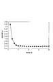
図13は、AD変換器の動作開始時から入力パルス信号φPLが遅延回路911内を周回する周回時間と周回数との関連を示した一例のグラフである。この図13においては、周回数が5回以内で入力パルス信号φPLが遅延回路911内を周回する周回時間が安定していない。
図13は、AD変換器の動作開始時から入力パルス信号φPLが遅延回路911内を周回する周回時間と周回数との関連を示した一例のグラフである。この図13においては、周回数が5回以内で入力パルス信号φPLが遅延回路911内を周回する周回時間が安定していない。
本発明は、上記の課題認識に基づいてなされたものであり、入力パルス信号を光電変換素子の入射光量に応じた遅延時間で周回させ、入力パルス信号の周回数に応じたデジタル値を出力するAD変換器を具備する光電変換装置において、AD変換器の動作開始後に出力されるデジタル値が不安定な期間のデジタル値を補正して良好なデジタル値を得ることができる光電変換装置を提供することを目的としている。
本発明に係る光電変換装置は、光電変換素子を有し、該光電変換素子への入射光量に応じた画素信号を出力する画素が二次元に複数配置された画素アレイと、前記画素アレイから読み出した前記画素信号をデジタル値に変換して出力する複数のAD変換器と、を備え、前記AD変換器は、前記画素アレイから読み出した前記画素信号の電圧の大きさに応じた遅延時間でパルス信号を遅延させる遅延ユニットを複数段接続したパルス遅延回路と、前記パルス信号が前記遅延ユニットを所定時間に通過した段数に基づいたデジタル値を出力するエンコーダ部と、前記エンコーダ部が出力したデジタル値を、予め定められた期間に前記パルス信号が前記遅延ユニットを通過した段数に相当する分だけ補正する補正手段と、を有する。
また、本発明の前記補正手段は、前記画素アレイから前記画素信号の読み出しを開始してから、予め定められた期間が経過するまでに前記パルス信号が前記遅延ユニットを通過した段数に相当するデジタル値を無効とするものとしてもよい。
また、本発明の前記補正手段は、前記エンコーダ部から出力されるデジタル値から予め定められた値を減算する減算手段を有するものとしてもよい。
また、本発明の前記補正手段は、前記エンコーダ部から出力されるデジタル値に応じて減算値を算出する演算手段と、前記エンコーダ部から出力されるデジタル値から、前記演算手段が算出した前記減算値を減算する減算手段と、を有するものとしてもよい。
また、本発明の前記補正手段は、前記画素アレイから前記画素信号の読み出しを開始してから、予め定められた期間が経過するまでに前記パルス信号が前記遅延ユニットを通過した段数に相当するデジタル値を記憶する記憶手段と、前記エンコーダ部から出力されるデジタル値から、前記記憶手段が記憶した前記デジタル値を減算する減算手段と、を有するものとしてもよい。
本発明によれば、光電変換装置に具備されたAD変換器の動作開始後に出力されるデジタル値が不安定な期間のデジタル値を補正することによって、AD変換器の動作が不安定な期間のデジタル値に含まれるノイズを低減することができるので、光電変換素子の入射光量に応じた画素信号をアナログ・デジタル変換して良好なデジタル値を得ることができる。
以下、図面を参照しつつ、本発明の好適な実施形態について説明する。ただし、本発明は以下の各実施形態に限定されるものではなく、例えばこれら実施形態の構成要素同士を適宜組み合わせてもよい。
図1は、本実施形態による光電変換装置の概略構成を示したブロック図である。図1において、光電変換装置1は、画素P11~P45、垂直走査回路4、CDS回路51~55(以下、CDS51~CDS55という)、水平走査回路6、制御回路7、AD変換器81~85(以下、ADC81~ADC85という)、から構成される。また、図1においては、画素P11~P45が4行5列の二次元に配置され、画素アレイ3として構成されている。なお、画素P11~P45のいずれか1つを示すときには「画素2」という。また、CDS51~CDS55をまとめて示すときには「CDS5」という。また、ADC81~ADC85をまとめて示すときには「ADC8」という。
画素P11~P45は、光電変換素子である。画素P11~P45は、垂直走査回路4によって自画素2が選択されると入射光量に応じたレベルの画素出力信号を出力する。また、画素P11~P45は画素アレイ3として4行5列の二次元に配置され、画素列毎に画素出力信号φP1~φP5を出力する。なお、画素P11~P45で示した画素Pに続く最初の数字は行の番号、最後の数値は列の番号を表す。
CDS51~CDS55は、画素アレイ3の各画素列に配置され、画素2から読み出された画素出力信号と、画素リセット信号との差分を、画素2が露光した画像データに対応する画素信号φC1~φC5としてADC81~ADC85に出力する。なお、CDS51~CDS55で示したCDS5に続く数字は、画素アレイ3の列の番号を示す。
ADC81~ADC85は、CDS51~CDS55から入力された画素信号φC1~φC5をアナログ・デジタル変換するAD変換器である。ADC81~ADC85は、入力された画素信号をアナログ・デジタル変換し、変換後のデジタル値を出力する。なお、ADC81~ADC85で示したADC8に続く数字は、画素アレイ3の列の番号を示す。
垂直走査回路4は、制御回路7から入力される垂直制御信号に応じて、画素アレイ3から読み出す画素2の行を選択する回路である。垂直走査回路4は、画素アレイ3から読み出す画素2の行に応じた行選択信号φSL1~φSL4を出力する。垂直走査回路4が、例えば、画素アレイ3の1行目を選択する場合は、行選択信号φSL1に選択レベル(例えば、“High”レベル)を画素アレイ3に出力し、その他選択されていない行選択信号φSL2~φSL4には非選択レベル(例えば、“Low”レベル)を画素アレイ3に出力する。
水平走査回路6は、制御回路7から入力される水平制御信号に応じて、ADC81~ADC85がアナログ・デジタル変換したデジタル値を列毎に出力させることによって光電変換装置の出力とする回路である。水平走査回路6は、ADC8から読み出すデジタル値の列に応じた列選択信号φH1~φH5をADC8へ出力する。水平走査回路6が、例えば、画素アレイ3の1列目のデジタル値を出力させる場合は、列選択信号φH1を出力許可レベル(例えば、“High”レベル)にしてADC8に出力し、その他出力されていない列選択信号φH2~φH5を出力不許可レベル(例えば、“Low”レベル)にしてADC8に出力する。続いて列選択信号φH2~φH5を順次、出力許可レベル(例えば、“High”レベルのとき)、その他出力しない列に対応する列選択信号φH1~φH5を出力不許可レベル(例えば、“Low”レベルのとき)にしてADC8に出力することによって、ADC8がアナログ・デジタル変換したデジタル値を順次出力させる。
制御回路7は、光電変換装置の全体を制御する回路である。制御回路7は、図示しない外部からの画像取り込み命令に応じて、垂直走査回路4を制御する垂直制御信号と、水平走査回路6を制御する水平制御信号とを出力する。
また、制御回路7は、CDS5およびADC8の動作(動作開始および動作停止)を制御する。
また、制御回路7は、CDS5およびADC8の動作(動作開始および動作停止)を制御する。
<第1実施形態>
次に、本実施形態の光電変換装置1のAD変換器について説明する。図2は、本実施形態による光電変換装置1に具備されたAD変換器の内の1つのAD変換器(ADC81)の第1の実施形態による概略構成を示したブロック図である。なお、その他のADC82~ADC85は、図2に示したADC81と同様である。図2において、ADC81は、遅延回路811、補正エンコーダ812、から構成される。また、補正エンコーダ812は、カウンタ回路8121、ラッチ&エンコーダ回路8122、加算器8123、制御信号生成部8124、から構成される。
次に、本実施形態の光電変換装置1のAD変換器について説明する。図2は、本実施形態による光電変換装置1に具備されたAD変換器の内の1つのAD変換器(ADC81)の第1の実施形態による概略構成を示したブロック図である。なお、その他のADC82~ADC85は、図2に示したADC81と同様である。図2において、ADC81は、遅延回路811、補正エンコーダ812、から構成される。また、補正エンコーダ812は、カウンタ回路8121、ラッチ&エンコーダ回路8122、加算器8123、制御信号生成部8124、から構成される。
ADC81は、図示しないアナログ・デジタル変換開始のタイミング信号に応じて、CDS51から入力された画素信号φC1のアナログ・デジタル変換を行う。また、図示しないアナログ・デジタル変換完了のタイミング信号に応じて、図示しないADC81内の出力制御回路に保持され、水平走査回路6から入力される列選択信号φH1に応じて図示しない出力制御回路に保持しているデジタル値を出力する。
遅延回路811は、電源電圧に応じた遅延量を持った複数のゲート回路(以下、遅延ユニットという)がリング状に接続され、入力パルスφPLを周回させるリングディレイライン(RDL)である。
例えば、初段の遅延ユニットを否定論理積回路(NANDゲート)で構成し、その他の遅延ユニットを否定回路(NOTゲート)で構成した場合は、初段のNANDゲートの、一方の入力端子に入力パルスφPLを入力し、もう一方の入力端子に最終段のNOTゲートの出力を入力して、遅延回路811が動作している時は常に最終のNOTゲートの出力を論理反転する。また、2段目以降のNOTゲートは、入力端子に入力された値を論理反転して出力端子に出力する。
例えば、初段の遅延ユニットを否定論理積回路(NANDゲート)で構成し、その他の遅延ユニットを否定回路(NOTゲート)で構成した場合は、初段のNANDゲートの、一方の入力端子に入力パルスφPLを入力し、もう一方の入力端子に最終段のNOTゲートの出力を入力して、遅延回路811が動作している時は常に最終のNOTゲートの出力を論理反転する。また、2段目以降のNOTゲートは、入力端子に入力された値を論理反転して出力端子に出力する。
遅延回路811の遅延ユニットには、電源電圧として入力信号、すなわち、アナログ・デジタル変換の対象となるCDS51から入力された画素信号φC1が印加され、各遅延ユニットは、それぞれ前段の遅延ユニットから入力された入力パルスφPLを該電源電圧(画素信号φC1)の電圧レベルと、基準電圧(図2においては、接地:GNDレベル)とのレベル差に応じた遅延時間をもって次段の遅延ユニットに出力する。リング状に接続された各遅延ユニットが同様に動作し、入力パルスφPLが前段から後段の遅延ユニットへ順次伝達されることにより、入力パルスφPLが遅延回路811内を周回する。
補正エンコーダ812は、入力パルスφPLが遅延回路811内の遅延ユニットを通過した段数を検出し、該通過段数をADC81がアナログ・デジタル変換した結果であるデジタル値として出力する回路である。
また、補正エンコーダ812は、ADC81の動作開始後に遅延回路811内を周回する入力パルスφPLの周回時間が安定しない期間(以下、遅延回路811内を周回する入力パルスφPLの周回時間が安定しない期間を「パルス不安定期間」という)に出力される不安定なデジタル値を初期化する。このことによって、パルス不安定期間にアナログ・デジタル変換された結果を無効とし、ADC81が出力するアナログ・デジタル変換結果のデジタル値を補正する。
なお、補正エンコーダ812から出力されたデジタル値は、図示しないアナログ・デジタル変換完了のタイミング信号に応じて、図示しないADC81内の出力制御回路に保持さる。
また、補正エンコーダ812は、ADC81の動作開始後に遅延回路811内を周回する入力パルスφPLの周回時間が安定しない期間(以下、遅延回路811内を周回する入力パルスφPLの周回時間が安定しない期間を「パルス不安定期間」という)に出力される不安定なデジタル値を初期化する。このことによって、パルス不安定期間にアナログ・デジタル変換された結果を無効とし、ADC81が出力するアナログ・デジタル変換結果のデジタル値を補正する。
なお、補正エンコーダ812から出力されたデジタル値は、図示しないアナログ・デジタル変換完了のタイミング信号に応じて、図示しないADC81内の出力制御回路に保持さる。
カウンタ回路8121は、入力パルスφPLが遅延回路811を周回した周回数を検出し、該検出した周回数(カウント値)を出力する回路である。
カウンタ回路8121は、入力パルスφPLが、遅延回路811の最終段を通過する毎にカウント値を1加算し、そのカウント値を出力する。
また、カウンタ回路8121は、リセット信号φRSの例えば、立ち上がりタイミングで入力パルスφPLが遅延回路811を周回した周回数を一時保管し、その後、リセット信号φRSの入力レベル(例えば、“High”レベル)が予め定められた期間保持されている場合は、一時保管した入力パルスφPLが遅延回路811を周回した周回数を初期化する。
カウンタ回路8121は、入力パルスφPLが、遅延回路811の最終段を通過する毎にカウント値を1加算し、そのカウント値を出力する。
また、カウンタ回路8121は、リセット信号φRSの例えば、立ち上がりタイミングで入力パルスφPLが遅延回路811を周回した周回数を一時保管し、その後、リセット信号φRSの入力レベル(例えば、“High”レベル)が予め定められた期間保持されている場合は、一時保管した入力パルスφPLが遅延回路811を周回した周回数を初期化する。
ラッチ&エンコーダ回路8122は、入力パルスφPLが遅延回路811内の遅延ユニットを通過した段数を検出し、該検出した通過段数を出力する回路である。
ラッチ&エンコーダ回路8122は、リセット信号φRSの例えば、立ち上がりタイミングで入力パルスφPLが周回している遅延回路811内の各遅延ユニットの値を一時保管し、その一時保管した遅延回路811内の各遅延ユニットの値を出力する。
ラッチ&エンコーダ回路8122は、リセット信号φRSの例えば、立ち上がりタイミングで入力パルスφPLが周回している遅延回路811内の各遅延ユニットの値を一時保管し、その一時保管した遅延回路811内の各遅延ユニットの値を出力する。
加算器8123は、カウンタ回路8121から入力された周回数と、ラッチ&エンコーダ回路8122から入力された通過段数とを処理し、入力信号、すなわち、アナログ・デジタル変換の対象となるCDS51から入力された画素信号φC1の応じたデジタル値をADC81がアナログ・デジタル変換した結果として出力する回路である。
加算器8123は、カウンタ回路8121から入力された周回数をADC81が出力するデジタル値の上位ビットとし、ラッチ&エンコーダ回路8122から入力された通過段数をADC81が出力するデジタル値の下位ビットとして処理する。
加算器8123は、カウンタ回路8121から入力された周回数をADC81が出力するデジタル値の上位ビットとし、ラッチ&エンコーダ回路8122から入力された通過段数をADC81が出力するデジタル値の下位ビットとして処理する。
なお、本発明において、カウンタ回路8121から入力された周回数と、ラッチ&エンコーダ回路8122から入力された通過段数とが、ADC81がアナログ・デジタル変換した結果としてのデジタル値において切り替わるビットの位置、すなわち、最終的なデジタル値への変換するための処理方法に関しては、規定しない。
制御信号生成部8124は、ADC81が出力するデジタル値を補正するために、遅延回路811と、カウンタ回路8121と、ラッチ&エンコーダ回路8122とに入力する制御信号を生成する回路である。
制御信号生成部8124は、図示しないアナログ・デジタル変換開始のタイミング信号が、アナログ・デジタル変換開始の状態となると、遅延回路811内を周回する入力パルスφPLを“High”レベルにして、CDS51から入力された画素信号φC1に応じた遅延時間で遅延回路811内を周回させる。また、制御信号生成部8124は、アナログ・デジタル変換完了のタイミング信号が、アナログ・デジタル変換完了の状態となると、遅延回路811内を周回する入力パルスφPLを“Low”レベルにして、遅延回路811内の周回を停止する。
制御信号生成部8124は、図示しないアナログ・デジタル変換開始のタイミング信号が、アナログ・デジタル変換開始の状態となると、遅延回路811内を周回する入力パルスφPLを“High”レベルにして、CDS51から入力された画素信号φC1に応じた遅延時間で遅延回路811内を周回させる。また、制御信号生成部8124は、アナログ・デジタル変換完了のタイミング信号が、アナログ・デジタル変換完了の状態となると、遅延回路811内を周回する入力パルスφPLを“Low”レベルにして、遅延回路811内の周回を停止する。
また、制御信号生成部8124は、パルス不安定期間中に、カウンタ回路8121を初期化(無効化)するためのリセット信号φRS(例えば、予め定められた期間“High”レベルとなるパルス)を出力する。また、制御信号生成部8124が出力するリセット信号φRSの立ち上がりタイミングは、アナログ・デジタル変換期間が終了したときに、カウンタ回路8121による入力パルスφPLが遅延回路811を周回した周回数を一時保管するタイミング信号と、ラッチ&エンコーダ回路8122による入力パルスφPLが周回している遅延回路811内の各遅延ユニットの値を一時保管するタイミング信号としても用いられる。
次に本実施形態の光電変換装置1において画像信号のデジタル値を出力するタイミングについて説明する。図3は、本実施形態による光電変換装置1の動作の概要を示したタイミングチャートである。なお、本説明においては、ADC81がアナログ・デジタル変換を行う画素アレイ3の1列目の画素P11および画素P21のデジタル値を取得する例について説明を行う。また、その他のADC82~ADC85は、図3に示すADC81のタイミングと同様である。
図3において、光電変換装置1は図示しない外部からの初期化がなされ、画素出力信号φP1は画素P11のリセット状態の電圧レベル、画素信号φC1は出力がないことを示す電圧レベルとなっている。また、入力パルスφPLとリセット信号φRSは、初期値(“Low”レベル)であり、カウンタ値は“0”である。
その後、図示しない外部から画像取り込み命令が入力されると、画素アレイ3が露光を行う。
その後、図示しない外部から画像取り込み命令が入力されると、画素アレイ3が露光を行う。
続いて、t1のタイミングで制御回路7は、画素P11を選択するための垂直制御信号を垂直走査回路4に出力し、垂直走査回路4から入力された行選択信号φSL1によって選択された画素P11は、入射光量に応じた画素出力信号φP1を出力する。なお、入力パルスφPLは、“Low”レベルであるため、遅延回路811は、非動作(スタンバイ)状態である。
続いて、t2のタイミングで、CDS51は、画素P11から入力された画素出力信号φP1と、画素リセット信号とに応じて、画素信号φC1をADC81に出力する。
また、制御信号生成部8124が、遅延回路811内を周回する入力パルスφPLを“High”レベルにすると、CDS51から入力された画素信号φC1の電圧レベルと、基準電圧(例えば、図2における、接地:GNDレベル)とのレベル差に応じた遅延時間で、入力パルスφPLが遅延回路811内を周回する。また、カウンタ回路8121およびラッチ&エンコーダ回路8122は、遅延回路811内の各遅延ユニットの検出を開始する。なお、t2のタイミングから開始される遅延ユニットの検出結果は、パルス不安定期間である。
また、制御信号生成部8124が、遅延回路811内を周回する入力パルスφPLを“High”レベルにすると、CDS51から入力された画素信号φC1の電圧レベルと、基準電圧(例えば、図2における、接地:GNDレベル)とのレベル差に応じた遅延時間で、入力パルスφPLが遅延回路811内を周回する。また、カウンタ回路8121およびラッチ&エンコーダ回路8122は、遅延回路811内の各遅延ユニットの検出を開始する。なお、t2のタイミングから開始される遅延ユニットの検出結果は、パルス不安定期間である。
続いて、t3のタイミングで、制御信号生成部8124は、リセット信号φRSを“High”レベルにしてカウンタ回路8121の検出結果を初期化(無効化)する。
続いて、予め定められた期間、すなわち、パルス不安定期間が終了すると、t4のタイミングで、制御信号生成部8124は、リセット信号φRSを“Low”レベルにしてカウンタ回路8121およびラッチ&エンコーダ回路8122の検出結果の初期化を解除する。このことにより、カウンタ回路8121およびラッチ&エンコーダ回路8122は、遅延回路811内の各遅延ユニットの検出を再開する。
なお、t2のタイミングからt4のタイミングまでの期間も入力パルスφPLは“High”レベルであるため、遅延回路811内の周回は継続している。このt4のタイミングまで入力パルスφPLが遅延回路811内の周回を継続することにより、入力パルスφPLの周回時間が安定する。
このことにより、カウンタ回路8121およびラッチ&エンコーダ回路8122は、入力パルスφPLの周回時間が安定した期間の検出を行うことができ、ADC81が出力するデジタル値の補正をすることができる。
このことにより、カウンタ回路8121およびラッチ&エンコーダ回路8122は、入力パルスφPLの周回時間が安定した期間の検出を行うことができ、ADC81が出力するデジタル値の補正をすることができる。
続いて、t5のタイミングで、アナログ・デジタル変換期間が終了し、制御信号生成部8124が、入力パルスφPLを“Low”レベルにすると、入力パルスφPLの遅延回路811内の周回が止まる。また、制御信号生成部8124は、リセット信号φRSを“High”レベルにする。このリセット信号φRSの立ち上がりタイミングで、カウンタ回路8121が検出した入力パルスφPLが遅延回路811を周回した周回数と、ラッチ&エンコーダ回路8122が検出した入力パルスφPLが遅延回路811内の遅延ユニットを通過した段数とが一時保管される。その後、加算器8123は、一時保管された周回数と、通過段数とを処理して、画素P11の入射光量に応じたデジタル値を出力する。
出力されたデジタル値は、図示しないADC81内の出力制御回路に保持される。その後、水平走査回路6から入力された列選択信号φH1によってADC81が選択されると、図示しないADC81内の出力制御回路に保持されたデジタル値、すなわち、画素P11の入射光量に応じたデジタル値をアナログ・デジタル変換した結果として出力する。
続いて、t6のタイミングで、画素P11に対するアナログ・デジタル変換結果が初期化される。
続いて、t7のタイミングで制御回路7は、画素P21を選択するための垂直制御信号を垂直走査回路4に出力し、垂直走査回路4から入力された行選択信号φSL2によって選択された画素P21は、入射光量に応じた画素出力信号φP1を出力する。
以後、上述したt2のタイミング~t6のタイミングと同様に、ADC81は、画素P21に対するアナログ・デジタル変換を行い、水平走査回路6から入力された列選択信号φH1によってADC81が選択されると、画素P21の入射光量に応じたデジタル値をアナログ・デジタル変換した結果として出力する。
以後、上述したt2のタイミング~t6のタイミングと同様に、ADC81は、画素P21に対するアナログ・デジタル変換を行い、水平走査回路6から入力された列選択信号φH1によってADC81が選択されると、画素P21の入射光量に応じたデジタル値をアナログ・デジタル変換した結果として出力する。
以後、上述したt1のタイミング~t6のタイミングと同様に、ADC81は、画素P31および画素P41の入射光量に応じたデジタル値をアナログ・デジタル変換した結果として出力し、画素アレイ3のアナログ・デジタル変換、すなわち、光電変換装置1の全画像信号の読出しが完了する。
上記に述べたとおり、本発明の第1の実施形態によれば、画素Pの入射光量に応じたデジタル値をアナログ・デジタル変換する際に、パルス不安定期間に出力される不安定なデジタル値を補正することができるので、出力画像に現れるノイズが低減された良好な画像データ(デジタル値)を得ることができる。
また、特に電池やバッテリーによって動作するデジタルカメラ、デジタルビデオカメラなどに搭載される低消費電力のAD変換器(例えば、イメージャの信号処理に適応)においては、AD変換器を非動作状態から動作させることが多く発生するため、本発明によるデジタル値の補正による効果が高く、得られる出力信号のノイズが低減された良いデジタル値を得ることができる。
また、本実施形態においては、4行5列の二次元に配置された画素アレイ3の入射光量に応じたADC81~ADC85を配置した例について説明したが、複数画素を1列に構成したリニアセンサの出力をアナログ・デジタル変換するAD変換器に適応することもできる。
また、本実施形態においては、画素アレイ3とADC8との間にCDS5を配置した例について説明したが、CDS5を配置しなくても良く、画素出力信号の画素リセット信号と光信号の差分に相当する画素信号をADC8に入力するものであれば、同様にアナログ・デジタル変換をすることができる。
また、本実施形態においては、リセット信号φRSをt2のタイミング~t3のタイミングまでの間、初期値である“Low”レベルを維持している例について説明したが、リセット信号φRSをt2のタイミング~t3のタイミングまでの間、“High”レベルとする、すなわち、t2のタイミング~t4のタイミングまでの間をカウンタ回路8121のリセット期間とすることも可能である。このことにより、本実施形態におけるt2のタイミング~t3のタイミングまでの間のカウンタ回路8121の動作を停止させることができ、光電変換装置1の消費電力をより低減させることができる。
<第2実施形態>
以下、本発明の第2の実施形態について、図面を参照して説明する。図4は、第2の実施形態によるAD変換器(ADC810)の概略構成を示したブロック図である。図4において、ADC810は、遅延回路811、補正エンコーダ813、から構成される。また、補正エンコーダ813は、カウンタ回路8121、ラッチ&エンコーダ回路8122、加算器8123、制御信号生成部8134、補正部8135から構成される。
ADC810は、図1の光電変換装置1に示したADC81に置き換わるAD変換器であり、図2に示したADC81に対して、補正部8135が加算器8123の後段に追加され、制御信号生成部8124が制御信号生成部8134に変更されている。制御信号生成部8134は、図2に示した制御信号生成部8124とは、出力するリセット信号φRSのタイミングが異なる。
ADC810は、図2に示した第1実施形態のADC81と同様に、図示しないアナログ・デジタル変換開始のタイミング信号に応じて、CDS51から入力された画素信号φC1のアナログ・デジタル変換を行う。また、ADC810は、図示しないアナログ・デジタル変換完了のタイミング信号に応じて、アナログ・デジタル変換した結果を図示しないADC810内の出力制御回路に保持し、水平走査回路6から入力される列選択信号φH1に応じて、図示しない出力制御回路に保持しているデジタル値を出力する。
図4において、ADC810の遅延回路811、および補正エンコーダ813のカウンタ回路8121、ラッチ&エンコーダ回路8122、加算器8123は、図2に示した第1実施形態のADC81の対応するブロックと同じ動作を行う。
制御信号生成部8134は、ADC810が出力するデジタル値を補正するために、遅延回路811と、カウンタ回路8121と、ラッチ&エンコーダ回路8122と、補正部8135とに入力する制御信号を生成する回路である。
制御信号生成部8134が遅延回路811に対して生成する入力パルスφPLは、図2に示した制御信号生成部8124と同様である。
制御信号生成部8134が遅延回路811に対して生成する入力パルスφPLは、図2に示した制御信号生成部8124と同様である。
また、制御信号生成部8134は、ADC810によってアナログ・デジタル変換を開始するタイミングと、アナログ・デジタル変換を完了するタイミングとにカウンタ回路8121を初期化するためのリセット信号φRS(例えば、予め定められた期間“High”レベルとなるパルス)を出力する。また、制御信号生成部8134が出力するリセット信号φRSの立ち上がりタイミングは、アナログ・デジタル変換期間が終了したときに、カウンタ回路8121による入力パルスφPLが遅延回路811を周回した周回数を一時保管するタイミング信号と、ラッチ&エンコーダ回路8122による入力パルスφPLが周回している遅延回路811内の各遅延ユニットの値を一時保管するタイミング信号としても用いられる。
補正部8135は、加算器8123が出力したデジタル値から予め定められた一定のデジタル値を減算し、入力信号、すなわち、アナログ・デジタル変換の対象となるCDS51から入力された画素信号φC1に応じたデジタル値をADC810がアナログ・デジタル変換した結果として出力する回路である。
補正部8135は、演算回路35によって構成される。
補正部8135は、演算回路35によって構成される。
演算回路35は、加算器8123から入力されたデジタル値からパルス不安定期間に出力される不安定なデジタル値に対応する予め定められた一定のデジタル値を減算する演算回路である。
なお、本発明において、加算器8123が出力したデジタル値から減算する予め定められた一定のデジタル値の値、およびこのデジタル値の設定方法に関しては、規定しない。
なお、本発明において、加算器8123が出力したデジタル値から減算する予め定められた一定のデジタル値の値、およびこのデジタル値の設定方法に関しては、規定しない。
次に本第2の実施形態によるAD変換器におけるアナログ・デジタル変換のタイミングについて説明する。図5は、本第2の実施形態によるAD変換器におけるアナログ・デジタル変換の動作の概要を示したタイミングチャートである。なお、本説明においては、図1に示した光電変換装置1において、ADC81の位置に配置されるADC810が画素アレイ3の1列目の画素P11のアナログ・デジタル変換を行う例について説明を行う。
図5において、ADC810の駆動タイミングは、図3に示したADC81の駆動タイミングに対して、リセット信号φRSのタイミングが異なる。
また、その他の画素アレイ3の1列目の画素P21、画素P31、画素P41の入射光量に応じた画素出力信号φP1、およびADC82~ADC85に対応するAD変換器のタイミングは、図5に示すADC810のタイミングと同様である。
また、画素アレイ3が出力する画素出力信号φP1、CDS5が出力する画素信号φC1のタイミングは、図3に示すタイミングと同様である。
また、その他の画素アレイ3の1列目の画素P21、画素P31、画素P41の入射光量に応じた画素出力信号φP1、およびADC82~ADC85に対応するAD変換器のタイミングは、図5に示すADC810のタイミングと同様である。
また、画素アレイ3が出力する画素出力信号φP1、CDS5が出力する画素信号φC1のタイミングは、図3に示すタイミングと同様である。
図5において、図1に示した光電変換装置1に、図示しない外部からの初期化、および画像取り込み命令が入力され、垂直走査回路4から入力された行選択信号φSL1によって選択された画素P11の入射光量に応じた画素出力信号φP1が入力されると、t1のタイミングで制御信号生成部8134は、リセット信号φRSを“High”レベルとする。このことによって、カウンタ回路8121の検出結果を初期化する。
続いて、t2のタイミングで、制御信号生成部8134が、遅延回路811内を周回する入力パルスφPLを“High”レベルにすると、CDS51から入力された画素信号φC1の電圧レベルと、基準電圧(例えば、図4における、接地:GNDレベル)とのレベル差に応じた遅延時間で、入力パルスφPLが遅延回路811内を周回する。また、このt2のタイミングで制御信号生成部8134がリセット信号φRSを“Low”レベルにすることによって、カウンタ回路8121およびラッチ&エンコーダ回路8122は、遅延回路811内の各遅延ユニットの検出を開始する。なお、t2のタイミングから開始される遅延ユニットの検出結果は、パルス不安定期間を含む。
続いて、t3のタイミングで、アナログ・デジタル変換期間が終了し、制御信号生成部8134が、入力パルスφPLを“Low”レベルにすると、入力パルスφPLの遅延回路811内の周回が止まる。また、制御信号生成部8134は、リセット信号φRSを“High”レベルにする。このリセット信号φRSの立ち上がりタイミングで、カウンタ回路8121が検出した入力パルスφPLが遅延回路811を周回した周回数と、ラッチ&エンコーダ回路8122が検出した入力パルスφPLが遅延回路811内の遅延ユニットを通過した段数とが一時保管される。その後、加算器8123は、一時保管された周回数と、通過段数とを処理して、画素P11の入射光量に応じたデジタル値を補正部8135に出力する。
その後、補正部8135は、加算器8123が出力した画素P11の入射光量に応じたデジタル値から、パルス不安定期間に出力される不安定なデジタル値に対応する予め定められた一定のデジタル値を減算し、その結果のデジタル値(補正後のデジタル値)を出力する。
補正部8135から出力されたデジタル値は、図示しないADC810内の出力制御回路に保持され。その後、水平走査回路6から入力された列選択信号φH1によってADC810が選択されると、図示しないADC810内の出力制御回路に保持されたデジタル値、すなわち、画素P11の入射光量に応じたデジタル値をアナログ・デジタル変換した結果として出力する。
補正部8135から出力されたデジタル値は、図示しないADC810内の出力制御回路に保持され。その後、水平走査回路6から入力された列選択信号φH1によってADC810が選択されると、図示しないADC810内の出力制御回路に保持されたデジタル値、すなわち、画素P11の入射光量に応じたデジタル値をアナログ・デジタル変換した結果として出力する。
続いて、t4のタイミングで制御信号生成部8134がリセット信号φRSを“Low”レベルにすることによって、画素P11の入射光量に応じた画素出力信号φP1のアナログ・デジタル変換が完了する。
以後、上述したt1のタイミング~t4のタイミングと同様に、ADC810は、画素P21、画素P31および画素P41の入射光量に応じたデジタル値をアナログ・デジタル変換した結果として出力し、画素アレイ3のアナログ・デジタル変換、すなわち、光電変換装置1の全画像信号の読出しが完了する。
上記に述べたとおり、本発明の第2の実施形態においても、画素Pの入射光量に応じたデジタル値をアナログ・デジタル変換する際に、パルス不安定期間に出力される不安定なデジタル値を補正(減算)することができるので、出力画像に現れるノイズが低減された良好な画像データ(補正後のデジタル値)を得ることができる。
<第3実施形態>
以下、本発明の第3の実施形態について、図面を参照して説明する。図6は、第3の実施形態によるAD変換器(ADC820)の概略構成を示したブロック図である。図6において、ADC820は、遅延回路811、補正エンコーダ814、から構成される。また、補正エンコーダ814は、カウンタ回路8121、ラッチ&エンコーダ回路8122、加算器8123、制御信号生成部8134、補正部8145から構成される。
ADC820は、図1の光電変換装置1に示したADC81に置き換わるAD変換器であり、図4に示したADC810の補正部8135が補正部8145に変更されている。
補正部8145は、図4に示した補正部8135とは、内部の構成が異なる。
ADC820は、図2に示した第1実施形態のADC81と同様に、図示しないアナログ・デジタル変換開始のタイミング信号に応じて、CDS51から入力された画素信号φC1のアナログ・デジタル変換を行う。また、ADC820は、図示しないアナログ・デジタル変換完了のタイミング信号に応じて、アナログ・デジタル変換した結果を図示しないADC820内の出力制御回路に保持し、水平走査回路6から入力される列選択信号φH1に応じて、図示しない出力制御回路に保持しているデジタル値を出力する。
図6において、ADC820の遅延回路811、および補正エンコーダ814のカウンタ回路8121、ラッチ&エンコーダ回路8122、加算器8123は、図2に示した第1実施形態のADC81、および図4に示した第2実施形態のADC810の対応するブロックと同じ動作を行う。また、補正エンコーダ814の制御信号生成部8134は、図4に示した第2実施形態のADC810の対応するブロックと同じ動作を行う。
補正部8145は、加算器8123が出力したデジタル値に応じた補正係数を算出し、加算器8123が出力したデジタル値から、算出した補正係数に応じた補正値(デジタル値)を減算することによって、入力信号、すなわち、アナログ・デジタル変換の対象となるCDS51から入力された画素信号φC1の応じたデジタル値をADC820がアナログ・デジタル変換した結果として出力する回路である。
補正部8145は、演算回路45、補正係数算出部451、から構成される。
補正部8145は、演算回路45、補正係数算出部451、から構成される。
補正係数算出部451は、加算器8123から入力されたデジタル値からパルス不安定期間に応じて予め定められた一定の割合の補正係数を算出し、算出した補正係数に応じた補正値(デジタル値)を生成する演算回路である。
補正係数算出部451は、生成した補正値(デジタル値)を演算回路45に出力する。
例えば、図1の光電変換装置1が使用されている周囲の環境温度に対する該光電変換装置1の温度特性、すなわち、同じ画素信号φC1が入力された場合において、環境温度の差によって加算器8123から出力されるデジタル値の変化を予め測定しておき、環境温度差における補正の割合を補正係数とすることができる。例えば、該光電変換装置1の温度特性が、環境温度が10度高くなった場合、加算器8123から出力されるデジタル値が1割大きい値となるという温度特性であったとする。また、該光電変換装置1を動作させたときの環境温度を、温度センサー等によって測定した結果、該光電変換装置1の環境温度が、20度高くなっていることが測定されたとする。この測定された環境温度と、温度特性とから、加算器8123から出力されたデジタル値が2割大きい値であることが算出される。補正係数算出部451は、算出した2割という値を補正係数とする。また、算出した2割という補正係数を用いて、加算器8123から出力されたデジタル値の補正係数(2割)に対応する値を算出し、補正値とする。このことによって、該光電変換装置1が出力するデジタル値の環境温度の影響を低減することができる。
なお、本発明においては、補正係数の設定方法、算出方法に関しての規定はしない。
演算回路45は、加算器8123から入力されたデジタル値から、補正係数算出部451から入力された補正値(デジタル値)を減算する演算回路である。
また、本第3の実施形態によるAD変換器におけるアナログ・デジタル変換のタイミングは、図5に示した第2の実施形態によるAD変換器におけるアナログ・デジタル変換のタイミングと同様である。
ただし、t3のタイミングにおいて行われる加算器8123が出力した画素P11の入射光量に応じたデジタル値の補正は、補正係数算出部451によって、加算器8123から入力されたデジタル値からパルス不安定期間に応じて予め定められた一定の割合の補正係数に基づいて算出されたデジタル値(補正後のデジタル値)となる。
ただし、t3のタイミングにおいて行われる加算器8123が出力した画素P11の入射光量に応じたデジタル値の補正は、補正係数算出部451によって、加算器8123から入力されたデジタル値からパルス不安定期間に応じて予め定められた一定の割合の補正係数に基づいて算出されたデジタル値(補正後のデジタル値)となる。
上記に述べたとおり、本発明の第3の実施形態においても、画素Pの入射光量に応じたデジタル値をアナログ・デジタル変換する際に、パルス不安定期間に出力される不安定なデジタル値を補正係数によって補正することができるので、出力画像に現れるノイズが低減された良好な画像データ(補正後のデジタル値)を得ることができる。
<第4実施形態>
以下、本発明の第4の実施形態について、図面を参照して説明する。図7は、第4の実施形態によるAD変換器(ADC830)の概略構成を示したブロック図である。図7において、ADC830は、遅延回路811、補正エンコーダ815、から構成される。また、補正エンコーダ815は、カウンタ回路8121、ラッチ&エンコーダ回路8122、加算器8123、制御信号生成部8154、補正部8155から構成される。
ADC830は、図1の光電変換装置1に示したADC81に置き換わるAD変換器であり、図4に示したADC810の制御信号生成部8134が制御信号生成部8154に、補正部8135が補正部8155にそれぞれ変更されている。
ADC830は、図2に示した第1実施形態のADC81と同様に、図示しないアナログ・デジタル変換開始のタイミング信号に応じて、CDS51から入力された画素信号φC1のアナログ・デジタル変換を行う。また、ADC830は、図示しないアナログ・デジタル変換完了のタイミング信号に応じて、アナログ・デジタル変換した結果を図示しないADC830内の出力制御回路に保持し、水平走査回路6から入力される列選択信号φH1に応じて、図示しない出力制御回路に保持しているデジタル値を出力する。
図7において、ADC830の遅延回路811、および補正エンコーダ815のカウンタ回路8121、ラッチ&エンコーダ回路8122、加算器8123は、図2に示した第1実施形態のADC81、図4に示した第2実施形態のADC810、および図6に示した第3実施形態のADC820の対応するブロックと同じ動作を行う。また、補正エンコーダ815の制御信号生成部8154が生成する入力パルスφPLと、リセット信号φRSは、図4に示した第2実施形態のADC810、および図6に示した第3実施形態のADC820の対応するブロックと同じであるが、新たに補正部8155を制御するラッチ制御信号φLC1、およびラッチ制御信号φLC2が追加されている。
補正部8155は、加算器8123が出力したデジタル値を一時保存し、一時保存したデジタル値に基づいて補正を行うことによって、入力信号、すなわち、アナログ・デジタル変換の対象となるCDS51から入力された画素信号φC1の応じたデジタル値をADC830がアナログ・デジタル変換した結果として出力する回路である。
補正部8155は、第1のラッチ回路551、第2のラッチ回路552、演算回路55、から構成される。
補正部8155は、第1のラッチ回路551、第2のラッチ回路552、演算回路55、から構成される。
第1のラッチ回路551は、加算器8123から入力されたデジタル値を、制御信号生成部8154から入力されたラッチ制御信号φLC1に応じて(例えば、ラッチ制御信号φLC1の立ち上がりタイミングで)一時保存する回路である。
第2のラッチ回路552は、加算器8123から入力されたデジタル値を制御信号生成部8154から入力されたラッチ制御信号φLC2に応じて(例えば、ラッチ制御信号φLC2の立ち下がりタイミングで)一時保存する回路である。
第2のラッチ回路552は、加算器8123から入力されたデジタル値を制御信号生成部8154から入力されたラッチ制御信号φLC2に応じて(例えば、ラッチ制御信号φLC2の立ち下がりタイミングで)一時保存する回路である。
演算回路55は、第2のラッチ回路552に一時保存されているデジタル値から、第1のラッチ回路551に一時保存されているデジタル値を減算する演算回路である。
制御信号生成部8154は、ADC830が出力するデジタル値を補正するために、遅延回路811と、カウンタ回路8121と、ラッチ&エンコーダ回路8122と、補正部8155とに入力する制御信号を生成する回路である。
制御信号生成部8154が遅延回路811に対して生成する入力パルスφPL、およびリセット信号φRSは、図4および図6に示した制御信号生成部8134と同様である。
制御信号生成部8154が遅延回路811に対して生成する入力パルスφPL、およびリセット信号φRSは、図4および図6に示した制御信号生成部8134と同様である。
また、制御信号生成部8154は、パルス不安定期間が終了するタイミングで第1のラッチ回路551に加算器8123から入力されたデジタル値を一時保存するためのラッチ制御信号φLC1(例えば、予め定められた期間“High”レベルとなるパルス)を出力する。
また、制御信号生成部8154は、アナログ・デジタル変換期間が終了するタイミングで第2のラッチ回路552に加算器8123から入力されたデジタル値を一時保存するためのラッチ制御信号φLC2(例えば、予め定められた期間“High”レベルとなるパルス)を出力する。
また、制御信号生成部8154は、アナログ・デジタル変換期間が終了するタイミングで第2のラッチ回路552に加算器8123から入力されたデジタル値を一時保存するためのラッチ制御信号φLC2(例えば、予め定められた期間“High”レベルとなるパルス)を出力する。
上記に述べた構成とすることによって、予め定められた期間、すなわち、パルス不安定期間に出力される不安定なデジタル値を第1のラッチ回路551に一時保存し、パルス不安定期間を含むアナログ・デジタル変換期間全体のデジタル値を第2のラッチ回路552に一時保存することができる。
その後、補正部8155の演算回路55によって、第2のラッチ回路552に一時保存されているデジタル値、すなわち、パルス不安定期間を含むアナログ・デジタル変換期間全体のデジタル値から、第1のラッチ回路551に一時保存されているデジタル値、すなわち、パルス不安定期間に出力される不安定なデジタル値を減算し、その結果のデジタル値(補正後のデジタル値)を得ることができる。
その後、補正部8155の演算回路55によって、第2のラッチ回路552に一時保存されているデジタル値、すなわち、パルス不安定期間を含むアナログ・デジタル変換期間全体のデジタル値から、第1のラッチ回路551に一時保存されているデジタル値、すなわち、パルス不安定期間に出力される不安定なデジタル値を減算し、その結果のデジタル値(補正後のデジタル値)を得ることができる。
補正部8155から出力されたデジタル値は、図示しないADC830内の出力制御回路に保持される。その後、水平走査回路6から入力された列選択信号φH1によってADC830が選択されると、図示しないADC830内の出力制御回路に保持されたデジタル値、すなわち、画素P11の入射光量に応じたデジタル値をアナログ・デジタル変換した結果として出力する。
次に本第4の実施形態によるAD変換器におけるアナログ・デジタル変換のタイミングについて説明する。図8は、本第4の実施形態によるAD変換器におけるアナログ・デジタル変換の動作の概要を示したタイミングチャートである。なお、本説明においては、図1に示した光電変換装置1において、ADC81の位置に配置されるADC830が画素アレイ3の1列目の画素P11のアナログ・デジタル変換を行う例について説明を行う。
図8において、ADC830の駆動タイミングは、図5に示したADC81の駆動タイミングと同様であるが、新たに補正部8155を制御するラッチ制御信号φLC1、およびラッチ制御信号φLC2の出力タイミングが追加されている。
また、その他の画素アレイ3の1列目の画素P21、画素P31、画素P41の入射光量に応じた画素出力信号φP1、およびADC82~ADC85に対応するAD変換器のタイミングは、図5に示すADC810のタイミングと同様である。
また、画素アレイ3が出力する画素出力信号φP1、CDS5が出力する画素信号φC1のタイミングは、図3に示すタイミングと同様である。
また、その他の画素アレイ3の1列目の画素P21、画素P31、画素P41の入射光量に応じた画素出力信号φP1、およびADC82~ADC85に対応するAD変換器のタイミングは、図5に示すADC810のタイミングと同様である。
また、画素アレイ3が出力する画素出力信号φP1、CDS5が出力する画素信号φC1のタイミングは、図3に示すタイミングと同様である。
図8において、図1に示した光電変換装置1に、図示しない外部からの初期化、および画像取り込み命令に応じて、画素P11からの画素出力信号φP1が入力されると、t1のタイミングで、図5に示したt1のタイミングと同様に、制御信号生成部8154は、リセット信号φRSを“High”レベルとして、カウンタ回路8121の検出結果を初期化する。
続いて、t2のタイミングで、図5に示したt2のタイミングと同様に、制御信号生成部8154が、遅延回路811内を周回する入力パルスφPLを“High”レベルにすることによって、CDS51から入力された画素信号φC1の電圧レベルと、基準電圧(例えば、図7における、接地:GNDレベル)とのレベル差に応じた遅延時間で、入力パルスφPLが遅延回路811内を周回し、また、制御信号生成部8154が、リセット信号φRSを“Low”レベルにすることによって、カウンタ回路8121およびラッチ&エンコーダ回路8122は、遅延回路811内の各遅延ユニットの検出を開始する。なお、t2のタイミングから開始される遅延ユニットの検出結果は、図5に示したタイミングチャートと同様に、パルス不安定期間を含む。
続いて、t3のタイミングで、パルス不安定期間が終了すると、制御信号生成部8154が、第1のラッチ回路551のラッチ制御信号φLC1(例えば、“High”パルス)を出力する。
このラッチ制御信号φLC1によって、第1のラッチ回路551は、パルス不安定期間に加算器8123から入力されたデジタル値、すなわち、パルス不安定期間に出力される不安定なデジタル値を一時保存する。
このラッチ制御信号φLC1によって、第1のラッチ回路551は、パルス不安定期間に加算器8123から入力されたデジタル値、すなわち、パルス不安定期間に出力される不安定なデジタル値を一時保存する。
続いて、t4のタイミングで、アナログ・デジタル変換期間が終了する直前に、制御信号生成部8154が、第2のラッチ回路552のラッチ制御信号φLC2(例えば、“High”パルス)を出力する。
このラッチ制御信号φLC2によって、第2のラッチ回路552は、パルス不安定期間を含むアナログ・デジタル変換期間全体のデジタル値を一時保存する。
このラッチ制御信号φLC2によって、第2のラッチ回路552は、パルス不安定期間を含むアナログ・デジタル変換期間全体のデジタル値を一時保存する。
その後、演算回路55は、第2のラッチ回路552に一時保存されているアナログ・デジタル変換期間全体のデジタル値から、第1のラッチ回路551に一時保存されているパルス不安定期間に出力される不安定なデジタル値を減算し、その結果のデジタル値(補正後のデジタル値)を出力する。
続いて、t5のタイミングで、図5に示したt3のタイミングと同様に、アナログ・デジタル変換期間が終了すると、制御信号生成部8154が、入力パルスφPLを“Low”レベルにすることによって、入力パルスφPLの遅延回路811内の周回が止まり、また、制御信号生成部8154が、リセット信号φRSを“High”レベルにすることによって、演算回路55が算出したデジタル値(補正後のデジタル値)が、図示しないADC830内の出力制御回路に保持される。
続いて、t6のタイミングで制御信号生成部8154が、リセット信号φRSを“Low”レベルにすることによって、画素P11の入射光量に応じた画素出力信号φP1のアナログ・デジタル変換が完了する。
図示しないADC830内の出力制御回路に保持された演算回路55が算出したデジタル値(補正後のデジタル値)は、水平走査回路6から入力された列選択信号φH1によってADC830が選択されることによって、図示しないADC830内の出力制御回路から読み出されて、画素P11の入射光量に応じたデジタル値をアナログ・デジタル変換した結果として出力される。
図示しないADC830内の出力制御回路に保持された演算回路55が算出したデジタル値(補正後のデジタル値)は、水平走査回路6から入力された列選択信号φH1によってADC830が選択されることによって、図示しないADC830内の出力制御回路から読み出されて、画素P11の入射光量に応じたデジタル値をアナログ・デジタル変換した結果として出力される。
以後、上述したt1のタイミング~t6のタイミングと同様に、ADC830は、画素P21、画素P31および画素P41の入射光量に応じたデジタル値をアナログ・デジタル変換した結果として出力し、画素アレイ3のアナログ・デジタル変換、すなわち、光電変換装置1の全画像信号の読出しが完了する。
上記に述べたとおり、本発明の第4の実施形態においても、画素Pの入射光量に応じたデジタル値をアナログ・デジタル変換する際に、パルス不安定期間に出力される不安定なデジタル値を補正(減算)することができるので、出力画像に現れるノイズが低減された良好な画像データ(補正後のデジタル値)を得ることができる。
なお、本第4の実施形態における補正部8155は、第1のラッチ回路551と第2のラッチ回路552を有する構成としたが、第1のラッチ回路551のみを備え、加算器8123から入力されたデジタル値から、第1のラッチ回路551に一時保存されているパルス不安定期間に出力される不安定なデジタル値を減算し、その結果のデジタル値(補正後のデジタル値)を出力する構成とすることもできる。この構成の場合、図8のt5のタイミングにおいて図5に示したt3のタイミングと同様に、制御信号生成部8154によって制御されるリセット信号φRSの立ち上がりタイミングで、カウンタ回路8121が検出した入力パルスφPLが遅延回路811を周回した周回数と、ラッチ&エンコーダ回路8122が検出した入力パルスφPLが遅延回路811内の遅延ユニットを通過した段数とが一時保管され、その後、加算器8123が処理することによって出力される画素P11の入射光量に応じたデジタル値を用いることによって、演算回路55によるデジタル値を補正(減算)が実現できる。
上記に述べたとおり、本発明を実施するための最良の形態によれば、光電変換装置に具備されたAD変換器の動作開始後に出力されるデジタル値が不安定な期間のデジタル値を補正することができるので、不安定な期間のデジタル値に含まれるノイズを低減した良好なデジタル値を得ることができる。
このことによって、本発明の光電変換装置を電池やバッテリーによって動作するデジタルカメラ、デジタルビデオカメラなどに搭載した場合に、光電変換装置に具備されたAD変換器の動作を積極的に停止することができ、該デジタルカメラ、デジタルビデオカメラなどの消費電力を低減することができる。
このことによって、本発明の光電変換装置を電池やバッテリーによって動作するデジタルカメラ、デジタルビデオカメラなどに搭載した場合に、光電変換装置に具備されたAD変換器の動作を積極的に停止することができ、該デジタルカメラ、デジタルビデオカメラなどの消費電力を低減することができる。
なお、本実施形態の遅延回路811における遅延ユニットは、電源側を入力信号、すなわち、アナログ・デジタル変換の対象となる画素信号φC1とし、接地側を基準電圧とした構成で説明したが、図9の遅延回路841に示すように、電源側を基準電圧とし、接地側を入力信号とした構成とすることもできる。
また、2種類の入力信号がある場合は、図10の遅延回路851に示すように電源側を第1の入力信号とし、接地側を第2の入力信号とした構成とすることもできる。また、図10の遅延回路851と逆に電源側を第2の入力信号とし、接地側を第1の入力信号とした構成とすることもできる。
また、2種類の入力信号がある場合は、図10の遅延回路851に示すように電源側を第1の入力信号とし、接地側を第2の入力信号とした構成とすることもできる。また、図10の遅延回路851と逆に電源側を第2の入力信号とし、接地側を第1の入力信号とした構成とすることもできる。
また、本実施形態の遅延回路は、初段の遅延ユニットを否定論理積回路(NANDゲート)で構成し、その他の遅延ユニットを否定回路(NOTゲート)で構成した場合について説明したが、本発明においては、遅延回路の構成は規定しない。すなわち、遅延回路は、入力信号の電圧レベルと基準電圧の電圧レベル、または2つの入力信号の電圧レベルのレベル差に応じた遅延時間をもって入力パルスを周回させる構成であれば、どのような構成であっても適用することができる。
以上、本発明の実施形態について、図面を参照して説明してきたが、具体的な構成はこの実施形態に限定されるものではなく、本発明の趣旨を逸脱しない範囲においての種々の変更も含まれる。
本発明は、光電変換素子の入射光量に応じた画素信号をアナログ・デジタル変換して、良好なデジタル値を得ることができる。
1 光電変換装置
2,P11,P12,P13,P14,P15,P21,P22,P23,P24,P25,P31,P32,P33,P34,P35,P41,P42,P43,P44,P45 画素
3 画素アレイ
4 垂直走査回路
5,51,52,53,54,55 CDS回路
6 水平走査回路
7 制御回路
8,81,82,83,84,85,810,820,830 AD変換器
811,841,851 遅延回路
812,813,814,815 補正エンコーダ
8121 カウンタ回路
8122 ラッチ&エンコーダ回路
8123 加算器
8124,8134,8154 制御信号生成部
8135,8145,8155 補正部
35,45,55 演算回路
451 補正係数算出部
551 第1のラッチ回路
552 第2のラッチ回路
90 画素ブロック
91 AD変換器
B1,B2,B3,B4,B5,B6,B7,B8,B9,B10,B11,B12,B13,B14,B15,B16,B17,B18,B19,B20 アレイブロック(サブアレイ)
911 遅延回路
912 エンコーダ
9121 カウンタ回路
9122 ラッチ&エンコーダ回路
9123 加算器
Claims (5)
- 光電変換素子を有し、該光電変換素子への入射光量に応じた画素信号を出力する画素が二次元に複数配置された画素アレイと、
前記画素アレイから読み出した前記画素信号をデジタル値に変換して出力する複数のAD変換器と、
を備え、
前記AD変換器は、
前記画素アレイから読み出した前記画素信号の電圧の大きさに応じた遅延時間でパルス信号を遅延させる遅延ユニットを複数段接続したパルス遅延回路と、
前記パルス信号が前記遅延ユニットを所定時間に通過した段数に基づいたデジタル値を出力するエンコーダ部と、
前記エンコーダ部が出力したデジタル値を、予め定められた期間に前記パルス信号が前記遅延ユニットを通過した段数に相当する分だけ補正する補正手段と、
を有する光電変換装置。 - 前記補正手段は、
前記画素アレイから前記画素信号の読み出しを開始してから、予め定められた期間が経過するまでに前記パルス信号が前記遅延ユニットを通過した段数に相当するデジタル値を無効とする、
請求項1に記載の光電変換装置。 - 前記補正手段は、
前記エンコーダ部から出力されるデジタル値から予め定められた値を減算する減算手段を有する、
請求項1に記載の光電変換装置。 - 前記補正手段は、
前記エンコーダ部から出力されるデジタル値に応じて減算値を算出する演算手段と、
前記エンコーダ部から出力されるデジタル値から、前記演算手段が算出した前記減算値を減算する減算手段と、
を有する、
請求項1に記載の光電変換装置。 - 前記補正手段は、
前記画素アレイから前記画素信号の読み出しを開始してから、予め定められた期間が経過するまでに前記パルス信号が前記遅延ユニットを通過した段数に相当するデジタル値を記憶する記憶手段と、
前記エンコーダ部から出力されるデジタル値から、前記記憶手段が記憶した前記デジタル値を減算する減算手段と、
を有する、
請求項1に記載の光電変換装置。
Priority Applications (1)
| Application Number | Priority Date | Filing Date | Title |
|---|---|---|---|
| US13/178,200 US8530816B2 (en) | 2009-01-09 | 2011-07-07 | Photoelectric conversion device having a correction unit to correct output of an analog-to-digital converter |
Applications Claiming Priority (2)
| Application Number | Priority Date | Filing Date | Title |
|---|---|---|---|
| JP2009003710A JP2010161723A (ja) | 2009-01-09 | 2009-01-09 | 光電変換装置 |
| JP2009-003710 | 2009-01-09 |
Related Child Applications (1)
| Application Number | Title | Priority Date | Filing Date |
|---|---|---|---|
| US13/178,200 Continuation US8530816B2 (en) | 2009-01-09 | 2011-07-07 | Photoelectric conversion device having a correction unit to correct output of an analog-to-digital converter |
Publications (1)
| Publication Number | Publication Date |
|---|---|
| WO2010079808A1 true WO2010079808A1 (ja) | 2010-07-15 |
Family
ID=42316573
Family Applications (1)
| Application Number | Title | Priority Date | Filing Date |
|---|---|---|---|
| PCT/JP2010/050106 Ceased WO2010079808A1 (ja) | 2009-01-09 | 2010-01-07 | 光電変換装置 |
Country Status (3)
| Country | Link |
|---|---|
| US (1) | US8530816B2 (ja) |
| JP (1) | JP2010161723A (ja) |
| WO (1) | WO2010079808A1 (ja) |
Families Citing this family (8)
| Publication number | Priority date | Publication date | Assignee | Title |
|---|---|---|---|---|
| JP5904899B2 (ja) * | 2012-08-06 | 2016-04-20 | オリンパス株式会社 | 撮像装置 |
| WO2014038140A1 (ja) * | 2012-09-10 | 2014-03-13 | パナソニック株式会社 | 固体撮像装置及び撮像装置 |
| JP6043650B2 (ja) * | 2013-02-22 | 2016-12-14 | オリンパス株式会社 | 撮像装置 |
| JP6108878B2 (ja) * | 2013-03-01 | 2017-04-05 | キヤノン株式会社 | 撮像装置、撮像装置の駆動方法、撮像システム、撮像システムの駆動方法 |
| KR102178825B1 (ko) * | 2013-11-15 | 2020-11-13 | 삼성전자 주식회사 | 픽셀 출력 레벨 제어 장치 및 이를 적용하는 이미지 센서 |
| KR102174192B1 (ko) * | 2014-01-14 | 2020-11-04 | 에스케이하이닉스 주식회사 | 프로세서 기반의 타이밍 생성 장치 및 그 방법과 그를 이용한 씨모스 이미지 센서 |
| JP6485674B1 (ja) * | 2017-09-14 | 2019-03-20 | パナソニックIpマネジメント株式会社 | 固体撮像装置、及びそれを備える撮像装置 |
| KR20210147347A (ko) * | 2020-05-28 | 2021-12-07 | 에스케이하이닉스 주식회사 | 이미지 센싱 장치 |
Citations (3)
| Publication number | Priority date | Publication date | Assignee | Title |
|---|---|---|---|---|
| JPH11230843A (ja) * | 1998-02-18 | 1999-08-27 | Denso Corp | センサ装置 |
| JP2001324390A (ja) * | 2000-05-17 | 2001-11-22 | Denso Corp | 熱型赤外線イメージセンサ |
| JP2006287879A (ja) * | 2005-04-05 | 2006-10-19 | Denso Corp | イメージセンサ及びイメージセンサの制御方法 |
Family Cites Families (1)
| Publication number | Priority date | Publication date | Assignee | Title |
|---|---|---|---|---|
| US6861969B1 (en) * | 2004-03-03 | 2005-03-01 | Analog Devices, Inc. | Methods and structures that reduce memory effects in analog-to-digital converters |
-
2009
- 2009-01-09 JP JP2009003710A patent/JP2010161723A/ja not_active Withdrawn
-
2010
- 2010-01-07 WO PCT/JP2010/050106 patent/WO2010079808A1/ja not_active Ceased
-
2011
- 2011-07-07 US US13/178,200 patent/US8530816B2/en not_active Expired - Fee Related
Patent Citations (3)
| Publication number | Priority date | Publication date | Assignee | Title |
|---|---|---|---|---|
| JPH11230843A (ja) * | 1998-02-18 | 1999-08-27 | Denso Corp | センサ装置 |
| JP2001324390A (ja) * | 2000-05-17 | 2001-11-22 | Denso Corp | 熱型赤外線イメージセンサ |
| JP2006287879A (ja) * | 2005-04-05 | 2006-10-19 | Denso Corp | イメージセンサ及びイメージセンサの制御方法 |
Also Published As
| Publication number | Publication date |
|---|---|
| JP2010161723A (ja) | 2010-07-22 |
| US8530816B2 (en) | 2013-09-10 |
| US20110290985A1 (en) | 2011-12-01 |
Similar Documents
| Publication | Publication Date | Title |
|---|---|---|
| WO2010079808A1 (ja) | 光電変換装置 | |
| JP6735582B2 (ja) | 撮像素子およびその駆動方法、および撮像装置 | |
| JP4786631B2 (ja) | 固体撮像装置、撮像装置 | |
| US7924336B2 (en) | Image pickup apparatus including a driving circuit to control a clamping switch so as to hold signals in holding capacitors | |
| US7859447B2 (en) | Image processing method, semiconductor device for detecting physical quantity distribution, and electronic apparatus | |
| JP5959834B2 (ja) | 撮像装置 | |
| JP2009033381A (ja) | 固体撮像装置およびその駆動方法 | |
| CN111491120A (zh) | 拍摄装置 | |
| US20060237721A1 (en) | Solid-state image pickup device, driving method for solid-state image pickup device, and image pickup apparatus | |
| US9258505B2 (en) | Imaging apparatus, imaging system, method for driving imaging apparatus, and method for driving imaging system | |
| JP4928069B2 (ja) | 撮像装置及び撮像システム | |
| JP4702571B2 (ja) | 列並列イメージセンサーの列オフセットの作成及び格納 | |
| US20180295307A1 (en) | Image sensing apparatus and control method therefor | |
| JP5378132B2 (ja) | 光電変換装置 | |
| JP5393360B2 (ja) | 光電変換装置 | |
| JP5956856B2 (ja) | 撮像素子及び撮像システム | |
| JP7312029B2 (ja) | 撮像信号の信号処理方法およびそれを用いた固体撮像装置 | |
| JP5933219B2 (ja) | 固体撮像装置 | |
| JP7098462B2 (ja) | 撮像装置および撮像装置の制御方法 | |
| JP6433276B2 (ja) | 撮像装置及びその制御方法、プログラム、記憶媒体 | |
| JP2024035623A (ja) | 光電変換装置、光電変換システムおよび光電変換方法 | |
| JP2012120044A (ja) | 光電変換装置 | |
| JP2011250304A (ja) | 光電変換装置 | |
| JP2019121924A (ja) | 撮像装置及び撮像装置の制御方法 | |
| JP2008154291A (ja) | 撮像装置及び撮像システム |
Legal Events
| Date | Code | Title | Description |
|---|---|---|---|
| 121 | Ep: the epo has been informed by wipo that ep was designated in this application |
Ref document number: 10729228 Country of ref document: EP Kind code of ref document: A1 |
|
| NENP | Non-entry into the national phase |
Ref country code: DE |
|
| 122 | Ep: pct application non-entry in european phase |
Ref document number: 10729228 Country of ref document: EP Kind code of ref document: A1 |