WO2010064650A1 - ガスセンサ - Google Patents
ガスセンサ Download PDFInfo
- Publication number
- WO2010064650A1 WO2010064650A1 PCT/JP2009/070230 JP2009070230W WO2010064650A1 WO 2010064650 A1 WO2010064650 A1 WO 2010064650A1 JP 2009070230 W JP2009070230 W JP 2009070230W WO 2010064650 A1 WO2010064650 A1 WO 2010064650A1
- Authority
- WO
- WIPO (PCT)
- Prior art keywords
- electrode
- thermistor
- gas sensor
- layer
- catalyst electrode
- Prior art date
- Legal status (The legal status is an assumption and is not a legal conclusion. Google has not performed a legal analysis and makes no representation as to the accuracy of the status listed.)
- Ceased
Links
Images




Classifications
-
- G—PHYSICS
- G01—MEASURING; TESTING
- G01N—INVESTIGATING OR ANALYSING MATERIALS BY DETERMINING THEIR CHEMICAL OR PHYSICAL PROPERTIES
- G01N27/00—Investigating or analysing materials by the use of electric, electrochemical, or magnetic means
- G01N27/02—Investigating or analysing materials by the use of electric, electrochemical, or magnetic means by investigating impedance
- G01N27/04—Investigating or analysing materials by the use of electric, electrochemical, or magnetic means by investigating impedance by investigating resistance
- G01N27/14—Investigating or analysing materials by the use of electric, electrochemical, or magnetic means by investigating impedance by investigating resistance of an electrically-heated body in dependence upon change of temperature
- G01N27/16—Investigating or analysing materials by the use of electric, electrochemical, or magnetic means by investigating impedance by investigating resistance of an electrically-heated body in dependence upon change of temperature caused by burning or catalytic oxidation of surrounding material to be tested, e.g. of gas
Definitions
- the present invention relates to a gas sensor that uses a combustible gas such as hydrogen gas as a detection target gas, and relates to a gas sensor that detects the detection target gas by converting heat generation or heat absorption by a catalyst into a change in resistance value of a thermistor.
- a gas sensor that detects the detection target gas by converting heat generation or heat absorption by a catalyst into a change in resistance value of a thermistor.
- hydrogen gas sensors for fuel cells have a low H 2 explosion limit of 4%, are capable of detecting trace amounts of gas at high speeds, and are exposed to harsh usage environments, so high environmental resistance is required.
- the realization of inexpensive sensors is also expected for widespread use of fuel cells.
- Patent Document 1 discloses a gas sensor that detects a detection target gas by converting an exothermic / endothermic reaction in a catalyst layer into a temperature resistance of a thermistor.
- the gas sensor of Patent Document 1 includes a thermistor layer 2 on a substrate 1 serving as a support, and both ends of the thermistor layer 2 so that a current flows in parallel to the film surface of the thermistor layer 2.
- the connected electrodes 3a and 3b, the thermistor layer 2 to prevent a short circuit between the electrodes 3a and 3b, the insulating layer 4 formed on the electrodes 3a and 3b, and the catalyst layer 5 formed on the insulating layer 4 Prepare.
- the electrodes 3a and 3b are connected to both ends of the thermistor layer 2 with a predetermined interval so that a current flows in parallel to the film surface of the thermistor layer 2.
- the material of the electrodes 3a and 3b is a metal material such as aluminum or platinum used for ordinary electrodes.
- the insulating layer 4 prevents a short circuit between the electrodes 3a and 3b, and an insulating resin, ceramics, or the like is used.
- the catalyst layer 5 is composed of a substance that interacts with the detection target gas to cause an exothermic or endothermic reaction.
- a substance that interacts with the detection target gas to cause an exothermic or endothermic reaction.
- an oxidation catalyst substance that catalyzes the oxidation of the detection target gas, a hydrogen storage alloy, or the like is used.
- a thin film thermistor layer 2 is formed on the substrate 1, and the electrical resistance value in the surface direction is detected. Since the thermistor layer 2 is a thin film, its sectional area is small and its resistance value is large. Therefore, the problem that the noise of an output signal becomes large arises.
- Patent Document 1 it is difficult to thermally separate the thermistor layer 2 and the substrate 1, so that the heat applied to the thermistor layer 2 escapes to the substrate 1 due to heat conduction. As a result, there is a problem that high detection sensitivity is difficult to obtain.
- an object of the present invention is to provide a gas sensor having high detection sensitivity and low output signal noise.
- the gas sensor of the present invention is configured as follows. (1) comprising a laminate in which a plurality of electrodes and a plurality of thermistor layers are laminated; At least one of the plurality of electrodes is a catalyst electrode that is disposed on the surface of the laminate and has a catalytic action that causes an exothermic reaction or an endothermic reaction by touching a detection target gas, At least one of the plurality of electrodes is an internal electrode disposed so that at least one thermistor layer of the plurality of thermistor layers is interposed between the electrode and the catalyst electrode.
- the resistance value in the layer direction (thickness direction) of the thermistor layer is detected, the resistance value is reasonably small. Therefore, the noise of the output signal can be reduced.
- a hollow portion is formed further inside than the internal electrode of the laminate.
- At least two of the plurality of electrodes are internal electrodes for temperature compensation elements arranged such that a thermistor layer that is not thermally coupled to the catalyst electrode among the plurality of thermistor layers is interposed. is there.
- temperature compensation can be performed, and stable sensitivity characteristics can be obtained in a wide temperature range.
- the size is not increased.
- a region in the laminated body that is opposite to a region where the catalyst electrode is formed with respect to the internal electrode located farthest from the catalyst electrode among the internal electrodes is insulative. You may be comprised with material. With this configuration, the contribution of the resistance value change in the detection region can be increased, and the detection sensitivity is increased.
- the external electrode may be made of a material that does not make ohmic contact with the thermistor layer.
- An ohmic electrode that is in ohmic contact with the thermistor layer on the surface of the laminate may be formed between the thermistor layer on the surface of the laminate and the catalyst electrode.
- a material in which the thermistor layer does not directly make ohmic contact with the catalyst electrode for example, a general positive temperature coefficient thermistor material can be used.
- a gas sensor with high detection sensitivity and low output signal noise can be configured.
- FIG. It is sectional drawing of the gas sensor 101 which concerns on 1st Embodiment. It is an example of the gas detection circuit using the gas sensor 101 which concerns on 1st Embodiment. It is sectional drawing of the gas sensor 102 which concerns on 2nd Embodiment. It is sectional drawing of the gas sensor 103 which concerns on 3rd Embodiment. It is sectional drawing of the gas sensor 104 which concerns on 4th Embodiment. It is sectional drawing of the gas sensor 105 which concerns on 5th Embodiment. It is sectional drawing of the gas sensor 106 which concerns on 6th Embodiment. It is sectional drawing of the gas sensor 107 which concerns on 7th Embodiment. It is sectional drawing of the gas sensor 108 which concerns on 8th Embodiment. It is sectional drawing of the gas sensor 109 which concerns on 9th Embodiment.
- FIG. 2 is a sectional view of the gas sensor 101 according to the first embodiment.
- the gas sensor 101 includes a laminate 10 of negative characteristic (NTC) thermistor ceramics, a catalyst electrode 11, an internal electrode 12, and external electrodes 13 and 14.
- NTC negative characteristic
- the surface layer portion from the internal electrode 12 to the exposed portion of the catalyst electrode 11 is a sensing portion.
- the catalyst electrode 11 generates heat or absorbs heat by a catalytic reaction by touching the detection target gas. As a result, the temperature of the thermistor layer immediately below the catalyst electrode 11 increases, and the resistance value of the thermistor layer decreases.
- the catalyst electrode 11 is electrically connected to the external electrode 14, and the internal electrode 12 is electrically connected to the external electrode 13. Therefore, with the external electrodes 13 and 14.
- the resistance value of the thermistor layer at the position sandwiched between the catalyst electrode 11 and the internal electrode 12 is detected.
- the NTC thermistor ceramic is a sintered body of a plurality of transition metal element oxides selected from, for example, Mn, Ni, Co, Fe, Cu, Al, Ti, and Zn.
- the catalyst electrode 11 is made of a substance that interacts with the detection target gas to cause an exothermic reaction or an endothermic reaction.
- an oxidation catalyst substance that catalyzes the oxidation of the detection target gas can be used. Accordingly, the gas to be detected can be appropriately selected.
- the detection target gas is hydrogen gas
- Pt and Pd are preferable in terms of reactivity to hydrogen gas.
- the internal electrode 12 is made of Ag, Pd, or an alloy thereof in ohmic contact with NTC thermistor ceramics. That is, since the catalyst electrode 11 has an ohmic junction with respect to the NTC thermistor ceramics, the catalyst electrode 11 and the internal electrode 12 can be made of the same electrode material.
- the overlapping area and distance between the catalyst electrode 11 and the internal electrode 12 are determined in consideration of the resistance change rate of the NTC thermistor ceramic so that the resistance value between the catalyst electrode 11 and the internal electrode 12 becomes a desired value. ing.
- the catalyst electrode 11 may be formed by sputtering after sintering the ceramic, but it is preferable to form it by a printing method such as screen printing before sintering the ceramic from the viewpoint of simplification of the process.
- the catalyst electrode 11 may be porous in order to improve the catalyst efficiency.
- porosity may be realized by adding a binder component or the like to the screen printing paste, or other methods may be used.
- the temperature of the catalyst electrode 11 rises.
- the heat generated by the catalyst electrode 11 raises the temperature of the thermistor layer between the catalyst electrode 11 and the internal electrode 12.
- a predetermined amount of Mn 3 O 4 , NiO, Co 3 O 4 , CuO, Fe 2 O 3 , TiO 2 , Al 2 O 3 and the like are weighed as ceramic raw materials, and then a grinding medium such as zirconia is included.
- the weighed product is put into a ball mill and sufficiently wet pulverized, and then calcined at a predetermined temperature to produce ceramic powder.
- a ceramic green sheet on which a catalyst electrode pattern is screen-printed is used as a lower layer, on which a ceramic green sheet on which an internal electrode pattern is screen-printed is superimposed, and an internal electrode pattern and a catalyst electrode pattern are printed thereon.
- a laminated substrate before sintering is prepared by laminating a predetermined layer of uncertain ceramic green sheets and press-bonding them.
- a ceramic green sheet on which neither the internal electrode pattern nor the catalyst electrode pattern is printed may be sandwiched between the ceramic green sheet on which the internal electrode pattern is printed and the ceramic green sheet on which the catalyst electrode pattern is printed.
- the steps (b) to (d) are treatments on a laminated substrate which is an aggregate of a plurality of laminated bodies, wherein the laminated substrate before sintering is individually separated into a laminated body before sintering. 10 and housed in a zirconia cage, and after removing the binder, firing was performed at a predetermined temperature (for example, 1000 to 1300 ° C.), and the internal electrode 12 and the catalyst electrode 11 were applied.
- the laminated body 10 of NTC thermistor ceramics is comprised.
- the external electrodes 13 and 14 may be formed by a thin film forming method such as a sputtering method or a vacuum evaporation method as long as the adhesion is good.
- an oxide such as Mn 3 O 4 is used as the ceramic raw material, but an Mn carbonate, hydroxide, or the like can also be used.
- the catalyst electrode 11 serves as a catalyst and an electrode for extracting an electric signal
- an insulating layer is unnecessary as compared with the structure for detecting the resistance value in the surface direction of the thin film thermistor layer as shown in FIG.
- the structure is very simple.
- the surface electrode is comb-shaped, and the resistance value is adjusted according to the number and interval of the surface electrode, so the design range is limited and the degree of freedom of the material (Especially the resistance change rate of the thermistor) is limited.
- the resistance value can be adjusted by the distance between the catalyst electrode 11 and the internal electrode 12 (the thermistor layer thickness) and the electrode overlap area. Therefore, the range of resistance value design is very wide, and the degree of freedom of the material is high. Further, since the resistance value is relatively small, the noise of the output signal can be reduced.
- FIG. 3 shows an example of a gas detection circuit using the gas sensor 101.
- a resistor Rs is a resistor by a thermistor of the sensing unit
- a resistor Rn is a temperature compensating thermistor.
- the resistors Rs and Rn and the resistors Ro and Ro constitute a resistor bridge circuit.
- the amplifier circuit AMP differentially amplifies the output voltage of the resistance bridge circuit.
- the output voltage Vout of the amplifier circuit AMP becomes a value corresponding to the resistance value of the resistor Rs by the thermistor by the gas detection circuit shown in FIG. Therefore, the output voltage Vout can be used as a gas detection signal.
- the gas to be detected can be detected by measuring the resistance value change due to the temperature rise through the catalyst electrode 11, the internal electrode 12, and the external electrodes 13 and 14.
- the NTC thermistor ceramic is used for the explanation.
- the present invention can also be applied to the case where the PTC thermistor ceramic is used.
- FIG. 4 is a cross-sectional view of the gas sensor 102 according to the second embodiment.
- the gas sensor 102 includes an NTC thermistor ceramic laminate 10, a catalyst electrode 11, an internal electrode 12, external electrodes 13 and 14, and a cavity 15.
- the configuration other than the cavity 15 is the same as that shown in FIG. 2 in the first embodiment.
- the hollow portion 15 is a surface layer portion of the laminate 10 and thermally separates the sensing portion where the catalyst electrode and the internal electrode are located from the other regions of the element body.
- the hollow portion 15 is formed by stacking several layers of the thermistor layers constituting the stacked body 10 as layers having openings.
- the heat is transmitted to the thermistor layer located on the opposite side of the internal electrode 12 from the catalyst electrode, but further away from the catalyst electrode. Since the cavity 15 exists in the region, it is thermally blocked here, and the heat is prevented from spreading to the entire laminate 10. In other words, the heat capacity of the sensing unit is small. Therefore, the temperature increase rate of the sensing part due to the catalytic reaction of the detection target gas is increased, and high responsiveness is obtained.
- the manufacturing method of the gas sensor 102 is basically the same as the process shown in the first embodiment. However, processing for forming the cavity 15 is performed on a predetermined ceramic green sheet among the multilayer ceramic green sheets on which no electrode pattern is printed.
- the ceramic green sheet of the layer having the cavity portion is formed with a hole for the cavity portion in the ceramic green sheet by laser processing or punching, and the hole is filled with an organic substance such as a binder, carbon paste, or the like. .
- an organic substance such as a binder, carbon paste, or the like.
- a predetermined plurality of layers among the plurality of ceramic green sheets on which neither the internal electrode pattern nor the catalyst electrode pattern is printed are defined as ceramic green sheets having the cavity pattern.
- the laminated substrate before sintering is produced by laminating in the order shown in the step (d) in the first embodiment and pressing.
- the obtained multilayer substrate is cut into predetermined dimensions to obtain individual unsintered laminates, which are accommodated in zirconia cages and subjected to binder removal treatment, and then at a predetermined temperature (for example, 1000 to 1300 ° C.) A baking treatment is applied.
- a predetermined temperature for example, 1000 to 1300 ° C.
- a baking treatment is applied.
- the laminate 10 including the catalyst electrode 11, the internal electrode 12, and the cavity 15 is configured.
- the NTC thermistor ceramic is used for the explanation.
- the present invention can also be applied to the case where the PTC thermistor ceramic is used.
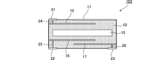
- FIG. 5 is a cross-sectional view of the gas sensor 103 according to the third embodiment.
- the gas sensor 103 includes the NTC thermistor ceramic laminate 10, the catalyst electrode 11, the internal electrode 12, the surface electrode 21, the via electrode 24, the temperature compensation element internal electrodes 16 and 17, the back electrodes 22 and 23, the via electrodes 25 and 26, And a cavity 15 is provided.
- the surface electrode 21 is electrically connected to the internal electrode 12 through the via electrode 24.
- the back electrodes 22 and 23 are electrically connected to the temperature compensation element internal electrodes 16 and 17 through the via electrodes 25 and 26.
- the catalyst electrode 11 generates heat by touching the detection target gas, and the resistance value between the catalyst electrode 11 and the internal electrode 12 decreases.
- the catalyst electrode 11 and the surface electrode 21 are electrically connected to an external circuit by wire bonding or the like.
- the opposing areas and intervals of the temperature compensation element internal electrodes 16 and 17 are the same as the opposing areas and intervals of the catalyst electrode 11 and the internal electrode 12, respectively. Since the cavity 15 is interposed between the pair of the catalyst electrode 11 and the internal electrode 12 and the pair of the temperature compensation element internal electrodes 16 and 17, the catalyst electrode 11 touches the detection target gas and the temperature is increased. Even if it rises, the cavity insulates its heat. Therefore, the ambient temperature around the temperature compensation element internal electrodes 16 and 17 is maintained.
- the back electrodes 22 and 23 are electrically connected to the mounting portion.
- the resistance due to the thermistor layer between the catalyst electrode 11 and the internal electrode 12 is the resistance Rs shown in FIG. 3, the resistance due to the thermistor layer between the temperature compensation element internal electrodes 16 and 17 is the resistance Rn shown in FIG.
- FIG. 6 is a cross-sectional view of the gas sensor 104 according to the fourth embodiment.
- the gas sensor 104 includes a laminate 10 of positive characteristic (PTC) thermistor ceramics, a catalyst electrode 112, an ohmic electrode 111, an internal electrode 32, and external electrodes 33 and 34.
- PTC positive characteristic
- the fourth embodiment uses PTC thermistor ceramics.
- ceramics used as PTC thermistors and Pd electrodes that cause a catalytic reaction with the detection target gas do not make ohmic contact, so that ohmic contact with PTC thermistor ceramics can be obtained between the catalyst electrode 112 and the thermistor layer.
- An electrode 111 is interposed. As a result, since the heat generated by the catalyst electrode 112 is directly transmitted to the thermistor layer via the ohmic electrode 111, higher responsiveness can be obtained.
- the material of the ohmic electrode 111 and the internal electrode 32 is, for example, Ni, Cu or an alloy thereof, and is in ohmic contact with the PTC thermistor ceramic. Further, for example, Cr, Ni—Cu, Ag or the like can be used as the material of the external electrodes 33 and 34.
- an internal electrode paste mainly composed of Ni, or an internal electrode paste made of Ni, Cu or an alloy thereof screen printing is performed on a ceramic green sheet to form an internal electrode pattern.
- an internal electrode paste containing Ni as a main component or an internal electrode paste made of Ni, Cu or an alloy thereof is screen-printed on a ceramic green sheet to form an ohmic electrode pattern.
- a Pd electrode paste is screen-printed on the printed ohmic electrode pattern to form a catalyst electrode pattern.
- a ceramic green sheet on which an ohmic electrode pattern and a catalyst electrode pattern are screen-printed is used as a lower layer, and a ceramic green sheet on which an internal electrode pattern is screen-printed thereon is overlaid thereon.
- a predetermined number of layers of ceramic green sheets on which no pattern is printed are laminated and pressed to produce a laminated substrate before sintering.
- a ceramic green sheet on which neither the internal electrode pattern nor the catalyst electrode pattern is printed may be sandwiched between the ceramic green sheet on which the internal electrode pattern is printed and the ceramic green sheet on which the catalyst electrode pattern is printed.
- the laminated substrate which is an aggregate before sintering, is cut into individual laminated bodies 10, accommodated in zirconia cages, and subjected to a binder removal treatment, and then a predetermined temperature (for example, 1000 to 1300 ° C.). ) To form a laminate 10 of PTC thermistor ceramics.
- External electrodes 13 and 14 such as Cr, Ni-Cu, Ag, etc. are formed on both ends of each laminate 10 by a thin film forming method such as sputtering or vacuum deposition.
- the gas sensor 101 is manufactured by the above process.
- an oxide such as BaO is used as a ceramic raw material, but a carbonate or hydroxide of Ba can also be used.
- the catalyst electrode layer 112 acts as a catalyst electrode, and is ohmically joined to the PTC thermistor ceramic via the ohmic electrode layer 111. Therefore, while being a PTC thermistor, the catalyst electrode can be used as one electrode for detecting the resistance value of the thermistor layer.
- a PTC thermistor as the thermistor layer, a high resistance temperature coefficient can be obtained, and a large change in output signal can be obtained even with the same temperature change. For this reason, sensitivity and responsiveness are improved.
- the resistance value of the thermistor can be reduced and the noise of the output signal can be reduced.
- the temperature compensation element internal electrodes 16 and 17 shown in FIG. 5 are provided in the gas sensor 101 or 102 shown in FIG. 2 or FIG. 4, and one of the temperature compensation element internal electrodes 16 is electrically connected to the external electrode 13.
- the other temperature compensation element internal electrode 17 may be drawn out to the lower surface of the multilayer body 10 through a via.
- the cavity 15 shown in FIG. 4 may be formed in the gas sensor 104 shown in FIG.
- the gas sensor 104 shown in FIG. 4 is provided with the temperature compensation element internal electrodes 16, 17 shown in FIG. 5, one temperature compensation element internal electrode 16 is electrically connected to the external electrode 13, and the other temperature compensation element.
- the internal electrode 17 may be drawn out to the lower surface of the stacked body 10 through a via.
- FIG. 7 is a cross-sectional view of the gas sensor 105 according to the fifth embodiment.
- the gas sensor 105 includes a laminate 10 of positive characteristic (PTC) thermistor ceramics, a catalyst electrode 11, internal electrodes 32 and 38, and external electrodes 33 and 34.
- PTC positive characteristic
- the surface layer portion from the internal electrode 38 to the exposed portion of the catalyst electrode 11 is a sensing portion.
- the catalyst electrode 11 generates heat or absorbs heat by a catalytic reaction by touching the detection target gas. As a result, the temperature of the thermistor layer immediately below the catalyst electrode 11 increases, and the resistance value of the thermistor layer between the internal electrode 32 and the internal electrode 38 decreases.
- the catalyst electrode 11 is not directly connected to the internal electrodes 32 and 38. That is, it is not used for detecting the resistance value of the thermistor layer of the sensing unit.
- the internal electrodes 32 and 38 are electrically connected to the external electrodes 33 and 34, respectively. Therefore, the resistance value of the thermistor layer at the position sandwiched between the internal electrode 32 and the internal electrode 38 is detected by the external electrodes 33 and 34.
- the thermistor ceramics are, for example, PTC thermistor ceramics, which are BT semiconductor ceramics whose resistance value changes with temperature change, and may include rare earth, strontium for CP adjustment, manganese for property improvement, and the like.
- the resistance values of the internal electrodes 32 and 38 can be determined by their overlapping areas and gaps, in order to obtain a desired resistance value, the overlapping areas and gaps of the internal electrodes 32 and 38 according to the rate of change in resistance of the ceramics. Adjust.
- the catalyst electrode 11 is made of a substance that interacts with the detection target gas to cause an exothermic reaction or an endothermic reaction.
- an oxidation catalyst substance that catalyzes the oxidation of the detection target gas or a hydrogen storage alloy can be used. Accordingly, the gas to be detected can be appropriately selected.
- the detection target gas is hydrogen gas
- Pt and Pd are preferable in terms of reactivity to hydrogen gas.
- the catalyst electrode 11 may be formed by sputtering after sintering the ceramic, but it is preferable to form the catalyst electrode 11 on the ceramic green sheet before sintering by a method such as screen printing from the viewpoint of simplification of the process.
- the catalyst electrode may be porous.
- a binder component or the like may be added to the screen printing paste, or another method may be used.
- you may contain the oxide component contained in ceramics. Processes other than the catalyst electrode forming process of the gas sensor 105 are the same as those shown in the fourth embodiment.
- the catalyst electrode 11 only needs to generate heat or absorb heat by the detection target gas, and the catalyst electrode 11 and the thermistor layer do not have to be in ohmic contact. Therefore, even if the thermistor ceramic is a PTC thermistor, the catalyst electrode 11 has Pt or A precious metal such as Pd can be used as it is. That is, the ohmic electrode layer 111 as shown in FIG. 6 in the fourth embodiment is not necessary. Therefore, the process for constituting the laminated structure can be simplified and the cost can be reduced.
- the PTC thermistor ceramic is used for explanation, but the present invention can also be applied to the case where NTC thermistor ceramic is used.
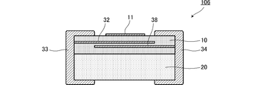
- FIG. 8 is a cross-sectional view of the gas sensor 106 according to the sixth embodiment.
- the gas sensor 106 includes a laminate 10 of positive characteristic (PTC) thermistor ceramics, a laminate 20 of insulating ceramics, a catalyst electrode 11, internal electrodes 32 and 38, and external electrodes 33 and 34.
- PTC positive characteristic
- the region on the opposite side is composed of a laminate 20 of insulating ceramics.
- the ceramic layer located on the opposite side of the region where the catalyst electrode is formed from the internal electrode 38 located farthest from the catalyst electrode is a region that does not directly contribute to the detection region of the gas sensor. If the thermistor ceramic layer is present in this portion, the resistance of the thermistor ceramic layer is equivalently connected in parallel between the external electrodes 33-34. Therefore, as shown in FIG. 8, by configuring the insulating ceramic layer in the region that does not directly contribute to the detection region of the gas sensor, the contribution of the resistance value change to the gas detection in the detection region can be increased. Greater sensitivity can be obtained.
- Rare earth oxides such as BaO, TiO 2 , SrCO 3 , (La 2 O 3, Nd 2 O 3, Sm 2 O 3 ), alkaline earth metal oxides such as CaO, Mn 3 O 4 or any of transition metal oxides such as 4 is weighed in a predetermined amount, and then the weighed material is put into a ball mill containing a grinding medium such as zirconia and sufficiently wet pulverized, and then at a predetermined temperature. And calcining to produce ceramic powder.
- a grinding medium such as zirconia and sufficiently wet pulverized
- the ceramic green sheet on which the pattern of the catalyst electrode 11 is screen-printed is used as a lower layer, and the ceramic green sheet on which the internal electrode pattern is screen-printed is overlaid thereon.
- a laminated body is produced by laminating a predetermined number of unprinted ceramic green sheets and press-bonding them.
- BT BiTiO 3
- External electrodes 33 and 34 such as Cr, Ni-Cu, and Ag are formed on both ends of the aggregate by a thin film forming method such as sputtering or vacuum deposition.
- the gas sensor 106 is manufactured by the above process.
- the PTC thermistor ceramic is used for explanation.
- the present invention can be applied to the case where NTC thermistor ceramic is used.
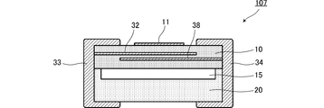
- FIG. 9 is a cross-sectional view of the gas sensor 107 according to the seventh embodiment.
- the gas sensor 107 includes a laminate 10 of positive characteristic (PTC) thermistor ceramics, a laminate 20 of insulating ceramics, a cavity 15, a catalyst electrode 11, internal electrodes 32 and 38, and external electrodes 33 and 34.
- the configuration other than the cavity 15 is the same as that shown in FIG. 8 in the sixth embodiment.
- the hollow portion 15 is a surface layer portion of the laminate 10 and thermally separates the sensing portion where the catalyst electrode and the internal electrode are located from the other regions of the element body.
- the hollow portion 15 is formed by stacking several layers of the thermistor layers constituting the stacked body 10 as layers having openings.
- the heat is transmitted to the thermistor layer located on the opposite side of the internal electrode 32 from the catalyst electrode, but further away from the catalyst electrode. Since the cavity 15 is present in the region, it is thermally blocked here, and the heat is prevented from spreading to the entire laminates 10 and 20. In other words, the heat capacity of the sensing unit is small. Therefore, the temperature increase rate of the sensing part due to the catalytic reaction of the detection target gas is increased, and high responsiveness is obtained.
- the manufacturing method of the gas sensor 107 is the same as that shown in the sixth embodiment except for the cavity 15.
- a hole for the hollow portion is formed in the ceramic green sheet by laser processing or punching, and an organic substance such as a binder, carbon paste, or the like is filled in the hole.
- an organic substance such as a binder, carbon paste, or the like is filled in the hole.
- a predetermined plurality of layers are used as the ceramic green sheets having the cavity pattern.
- the PTC thermistor ceramic is used for explanation, but the present invention can also be applied to the case where NTC thermistor ceramic is used.
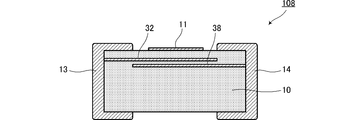
- FIG. 10 is a cross-sectional view of the gas sensor 108 according to the eighth embodiment.
- the gas sensor 108 includes a laminate 10 of positive characteristic (PTC) thermistor ceramics, a catalyst electrode 11, internal electrodes 32 and 38, and external electrodes 13 and 14.
- PTC positive characteristic
- the surface layer portion from the internal electrode 38 to the exposed portion of the catalyst electrode 11 is a sensing portion.
- the catalyst electrode 11 generates heat or absorbs heat by a catalytic reaction by touching the detection target gas. As a result, the temperature of the thermistor layer immediately below the catalyst electrode 11 increases, and the resistance value of the thermistor layer between the internal electrode 32 and the internal electrode 38 decreases.
- the material of the internal electrodes 32 and 38 is a base metal such as Ni, Cu or an alloy thereof. Therefore, the internal electrodes 32 and 38 are in ohmic contact with the PTC thermistor ceramic.
- the material of the external electrodes 13 and 14 is a noble metal such as Ag, Pd, or an alloy thereof, and does not make ohmic contact with the PTC thermistor ceramic. Therefore, the external electrodes 13-14 are electrically connected to the internal electrodes 32, 38, but have an interface resistance higher than the resistance value of the sensing unit at the interface with the PTC thermistor ceramics.
- the resistance value between the external electrodes 13-14 is dominated by the resistance value of the PTC thermistor ceramic layer between the internal electrodes 32-38, and the contribution of the resistance value change to the gas detection in the detection region can be increased. And greater sensitivity can be obtained.
- NTC thermistor ceramics When NTC thermistor ceramics are used as the thermistor ceramics, NTC thermistor ceramics have the same effect by using base metal electrodes such as Cu, Ni or alloys thereof as the external electrodes.
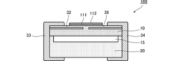
- FIG. 11 is a cross-sectional view of a gas sensor 109 according to the ninth embodiment.
- the gas sensor 109 includes a positive characteristic (PTC) thermistor ceramic laminate 10, an insulating ceramic laminate 20, a cavity 15, an ohmic electrode layer 111, a catalyst electrode 112, internal electrodes 32 and 38, and external electrodes 33 and 34. I have.
- PTC positive characteristic
- the point that the ohmic electrode layer 111 that makes ohmic contact with the PTC thermistor ceramics is provided is the same as the gas sensor 104 shown in FIG. Moreover, the point which is provided with the laminated body 20 and the cavity part 15 of insulating ceramics is the same as the gas sensor 107 shown in FIG.
- the internal electrodes 32 and 38 are in the same layer, and the thermistor ceramic layer between the internal electrodes 32 and 38 and the ohmic electrode layer 111 is a sensing part.
- the sensing part can be made thin (shallow), the heat capacity of the sensing part can be made smaller, and thus higher responsiveness can be obtained.
- the PTC thermistor ceramic is used for explanation, but the present invention can also be applied to the case where NTC thermistor ceramic is used.
Landscapes
- Chemical & Material Sciences (AREA)
- Chemical Kinetics & Catalysis (AREA)
- Electrochemistry (AREA)
- Physics & Mathematics (AREA)
- Health & Medical Sciences (AREA)
- Life Sciences & Earth Sciences (AREA)
- Analytical Chemistry (AREA)
- Biochemistry (AREA)
- General Health & Medical Sciences (AREA)
- General Physics & Mathematics (AREA)
- Immunology (AREA)
- Pathology (AREA)
- Investigating Or Analyzing Materials By The Use Of Electric Means (AREA)
Abstract
検出感度が高く、出力信号のノイズが小さいガスセンサを構成する。 ガスセンサ(102)は、サーミスタセラミックスの積層体(10)、触媒電極を構成する触媒電極(11)、内部電極(12)、及び外部電極(13,14)を備えている。触媒電極(11)に検出対象ガスが触れることによって触媒電極(11)が発熱し、感知部のサーミスタ層の抵抗値が低下する。触媒電極(11)の熱は絶縁層などを介することなくサーミスタ層に直接伝熱するので、検出感度が高い。また、感知部の熱は空洞部(15)で断熱され、拡散が阻止される構成にした場合、感知部の熱容量がより小さくなる。そのため、高感度で応答性の高いガスセンサとなる。
Description
この発明は、例えば水素ガス等の可燃性ガスを検出対象ガスとするガスセンサに関し、触媒による発熱又は吸熱をサーミスタの抵抗値変化に変換して検出対象ガスの検出を行うガスセンサに関するものである。
排出量が規制される自動車の排ガス、異常時に家庭用給湯器から排出される有毒ガス、近年の環境問題に対応すべく開発が急速に進む燃料電池など、我々を取り巻く環境には様々なガスが存在している。
自動車の排ガスであれば、CO2,NOx,SOx、家庭用給湯器であればCO、燃料電池であればH2などがそれにあたる。特にCOやH2などのガス漏れは、重大事故に繋がることから、検出対象ガスを正確かつ迅速に検出できるガスセンサの必要性は年々高まっている。
特に燃料電池用の水素ガスセンサなどは、H2の爆発限界が4%と低く、微量のガスを高速に検知する性能や、厳しい使用環境に曝されることから、高い耐環境性能が求められる。その一方で、燃料電池の広い普及のためには廉価なセンサの実現も期待されている。
Pt,Pd等の貴金属の触媒反応による吸熱、発熱を利用したガスセンサは従来幾つか提案されている。特に、触媒層での発熱・吸熱反応をサーミスタの温度抵抗に変換して検出対象ガスの検出するようにしたガスセンサが特許文献1に開示されている。
ここで、図1を基に、特許文献1に示されているガスセンサの作用について説明する。
特許文献1のガスセンサは、図1に示されるように、支持体となる基板1上にサーミスタ層2と、サーミスタ層2に対して膜面に平行に電流を流すようにサーミスタ層2の両端に接続された電極3a,3bと、電極3a,3b間の短絡を防ぐようサーミスタ層2、電極3a,3b上に形成された絶縁層4と、絶縁層4上に形成された触媒層5とを備える。
特許文献1のガスセンサは、図1に示されるように、支持体となる基板1上にサーミスタ層2と、サーミスタ層2に対して膜面に平行に電流を流すようにサーミスタ層2の両端に接続された電極3a,3bと、電極3a,3b間の短絡を防ぐようサーミスタ層2、電極3a,3b上に形成された絶縁層4と、絶縁層4上に形成された触媒層5とを備える。
電極3a,電極3bは、サーミスタ層2の膜面に平行に電流を流すように、所定間隔を有してサーミスタ層2の両端に接続される。電極3a,3bの材料としては通常の電極に用いられるアルミニウム、白金等の金属材料等である。
絶縁層4は、電極3a,3b間の短絡を防止するものであり、絶縁性の樹脂やセラミックス等が用いられる。
触媒層5は、検出対象ガスと相互作用して発熱又は吸熱反応を引き起こす物質で構成され、例えば検出対象ガスの酸化を触媒する酸化触媒物質や、水素吸蔵合金等が使用される。
特許文献1の構成では、[サーミスタ層2/絶縁層4/触媒層5]という構造を成していて、触媒層4とサーミスタ層2とを電気的に絶縁している。これは、触媒層5が貴金属層であるため、絶縁層を設けないと、電気信号が取り出せない(触媒層の電気抵抗値が支配的になる)ためである。
この場合、絶縁層4が熱伝導を阻害するため、高い検出感度が得にくいという問題がある。
また、特許文献1の構成では、基板1上に薄膜のサーミスタ層2を形成し、その面方向の電気抵抗値を検出することになる。サーミスタ層2は薄膜であるため、断面積が小さく、その抵抗値は大きい。そのため、出力信号のノイズが大きくなるという課題が生じる。
さらに特許文献1の構成では、サーミスタ層2と基板1との熱分離が困難であるので、サーミスタ層2に与えられた熱が熱伝導によって基板1へ逃げてしまう。その結果、高い検出感度が得にくいという問題がある。
そこで、この発明の目的は、検出感度が高く、出力信号のノイズが小さいガスセンサを提供することにある。
前記課題を解決するために、この発明のガスセンサは次のように構成する。
(1)複数の電極と複数のサーミスタ層が積層された積層体を備え、
前記複数の電極のうち少なくとも一つは、前記積層体の表面に配置され、検出対象ガスに触れることにより発熱反応又は吸熱反応を引き起こす触媒作用を有する触媒電極であり、
前記複数の電極のうち少なくとも一つは、前記触媒電極との間に前記複数のサーミスタ層のうちの少なくとも一つのサーミスタ層が介在するように配置された内部電極である。
(1)複数の電極と複数のサーミスタ層が積層された積層体を備え、
前記複数の電極のうち少なくとも一つは、前記積層体の表面に配置され、検出対象ガスに触れることにより発熱反応又は吸熱反応を引き起こす触媒作用を有する触媒電極であり、
前記複数の電極のうち少なくとも一つは、前記触媒電極との間に前記複数のサーミスタ層のうちの少なくとも一つのサーミスタ層が介在するように配置された内部電極である。
この構造により、触媒電極とサーミスタ層との間に絶縁層が無く、触媒電極での発熱又は吸熱がサーミスタ層に直接熱伝導するため、高い検出感度が得られる。
また、サーミスタ層の層方向(厚み方向)の電気抵抗値を検出することになるので、その抵抗値は適度に小さい。そのため、出力信号のノイズを小さくできる。
(2)例えば、前記積層体の前記内部電極より更に内部には空洞部を形成する。
この構造により、触媒電極及びこの触媒電極の発熱又は吸熱によって温度変化するサーミスタ層で構成される感知部と、それより積層体の内部との熱分離ができる。そのため、この感知部の熱容量を非常に小さくでき、感知部のサーミスタ層に与えられた熱が熱伝導によって積層体に内部へ逃げてしまうことがない。その結果、高い応答性が得られる。
この構造により、触媒電極及びこの触媒電極の発熱又は吸熱によって温度変化するサーミスタ層で構成される感知部と、それより積層体の内部との熱分離ができる。そのため、この感知部の熱容量を非常に小さくでき、感知部のサーミスタ層に与えられた熱が熱伝導によって積層体に内部へ逃げてしまうことがない。その結果、高い応答性が得られる。
(3)例えば、前記複数の電極のうち少なくとも2つの電極は、前記複数のサーミスタ層のうち前記触媒電極と熱的に結合しないサーミスタ層が介在するように配置された温度補償素子用内部電極である。
これにより、温度補償ができ、広い温度範囲で安定した感度特性が得られる。しかも、別途温度補償素子を設ける必要が無いので大型化することもない。
これにより、温度補償ができ、広い温度範囲で安定した感度特性が得られる。しかも、別途温度補償素子を設ける必要が無いので大型化することもない。
(4)前記積層体内の領域であって、前記内部電極のうち、前記触媒電極から最も離れた位置に位置する内部電極よりも前記触媒電極が形成される領域とは反対側の領域は絶縁性材料で構成されていてもよい。
この構成により、検知領域における抵抗値変化の寄与を大きくすることができ、検知感度が高まる。
この構成により、検知領域における抵抗値変化の寄与を大きくすることができ、検知感度が高まる。
(5)前記外部電極は、前記サーミスタ層とオーミック接触しない材料で構成されていてもよい。
この構成により、内部電極間のサーミスタ層での抵抗値変化が支配的となり、検知領域における抵抗値変化の寄与を大きくすることができ、検知感度が高まる。
この構成により、内部電極間のサーミスタ層での抵抗値変化が支配的となり、検知領域における抵抗値変化の寄与を大きくすることができ、検知感度が高まる。
(6)前記積層体の表面のサーミスタ層と前記触媒電極との間に、前記積層体の表面のサーミスタ層とオーミック接触するオーミック電極が形成されていてもよい。
この構成により、触媒電極に対してサーミスタ層が直接オーミック接触しないような材料、例えば一般的な正特性サーミスタ材料であっても利用できる。
この構成により、触媒電極に対してサーミスタ層が直接オーミック接触しないような材料、例えば一般的な正特性サーミスタ材料であっても利用できる。
この発明によれば、検出感度が高く、出力信号のノイズが小さいガスセンサが構成できる。
《第1の実施形態》
図2は第1の実施形態に係るガスセンサ101の断面図である。ガスセンサ101は、負特性(NTC)サーミスタセラミックスの積層体10、触媒電極11、内部電極12、及び外部電極13,14を備えている。
図2は第1の実施形態に係るガスセンサ101の断面図である。ガスセンサ101は、負特性(NTC)サーミスタセラミックスの積層体10、触媒電極11、内部電極12、及び外部電極13,14を備えている。
積層体10のうち、内部電極12から触媒電極11の露出部までの表層部が感知部である。触媒電極11は検出対象ガスに触れることで触媒反応により発熱又は吸熱する。これにより、触媒電極11の直下のサーミスタ層の温度が上昇し、そのサーミスタ層の抵抗値が低下する。
触媒電極11は外部電極14に導通し、内部電極12は外部電極13に導通する。したがって、外部電極13と14とによって。触媒電極11と内部電極12とで挟まれる位置のサーミスタ層の抵抗値が検出される。NTCサーミスタセラミックスは、例えばMn,Ni,Co,Fe,Cu,Al,Ti,Znなどから選ばれる複数の遷移金属元素酸化物の焼結体である。
触媒電極11は検出対象ガスと相互作用して発熱反応又は吸熱反応を引き起こす物質で構成されている。例えば検出対象ガスの酸化を触媒する酸化触媒物質を使用することができる。これらによって検出対象となるガスを適宜選択することができる。特に検出対象ガスが水素ガスである場合には、水素ガスへの反応性の面などからPtやPdが好ましい。
内部電極12は、NTCサーミスタセラミックスとオーミック接合するAg,Pd又はそれらの合金で構成されている。すなわち、触媒電極11はNTCサーミスタセラミックスに対してオーミック接合を有するので、触媒電極11と内部電極12とは同じ電極材料で構成することができる。
触媒電極11と内部電極12との重なり面積と距離は、触媒電極11と内部電極12との間の抵抗値が所望の値となるように、NTCサーミスタセラミックスの抵抗変化率を考慮して定められている。
触媒電極11は、セラミックスの焼結後にスパッタリングによって形成してもよいが、セラミックスの焼結前にスクリーン印刷などの印刷法で形成することが工程の簡便化などの点からは好ましい。当然、触媒効率の向上のために、触媒電極11が多孔質となっていてもよい。例えば、スクリーン印刷用ペーストにバインダ成分などを添加することで多孔化を実現してもよいし、他の方法を用いてもよい。また、セラミックスとの密着性を確保するために、セラミックスに含まれる金属酸化物成分を触媒電極用のペーストに共材として含有させてもよい。
以上に示した構成のガスセンサ101において、触媒電極11がPdを主成分として含んで、水素ガスを検出する場合について説明する。
検出対象ガス中に水素ガスが存在する場合、触媒電極に含まれるPdによって水素ガスが触媒作用を受けて発熱反応を起こせば、触媒電極11の温度が上昇する。この触媒電極11の発熱が触媒電極11と内部電極12との間のサーミスタ層の温度を上昇させる。この温度上昇による抵抗値変化を、外部電極13,14を通して測定することで水素ガスの存在の検出、又は水素ガス濃度の定量測定を行うことができる。
次に、ガスセンサ101の具体的な製造方法の例を順に示す。
(a)セラミックス素原料としてMn3O4、NiO、Co3O4、CuO、Fe2O3、TiO2、Al2O3などを所定量秤量し、次いでジルコニア等の粉砕媒体が内有されたボールミルに前記秤量物を投入して十分に湿式粉砕し、その後、所定の温度で仮焼し、セラミックス粉末を作製する。
(a)セラミックス素原料としてMn3O4、NiO、Co3O4、CuO、Fe2O3、TiO2、Al2O3などを所定量秤量し、次いでジルコニア等の粉砕媒体が内有されたボールミルに前記秤量物を投入して十分に湿式粉砕し、その後、所定の温度で仮焼し、セラミックス粉末を作製する。
(b)前記セラミックス粉末に有機バインダを加え、湿式で混合処理を行なってスラリー状とし、その後、ドクターブレード法等によってセラミックグリーンシートを作製する。
(c)Ag-Pdを主成分とした内部電極用ペーストを使用し、前記セラミックグリーンシート上にスクリーン印刷して内部電極パターンを形成する。また、Pd電極ペーストを使用し、内部電極と同様の方法でセラミックグリーンシート上にスクリーン印刷を施して触媒電極パターンを形成する。
(d)触媒電極パターンがスクリーン印刷されたセラミックグリーンシートを下層にし、その上に、内部電極パターンがスクリーン印刷されたセラミックグリーンシートを重ね、その上に、内部電極パターンも触媒電極パターンも印刷されていないセラミックグリーンシートを所定層積層し圧着することによって、焼結前の積層基板を作製する。
内部電極パターンが印刷されたセラミックグリーンシートと、触媒電極パターンが印刷されたセラミックグリーンシートとの間には、内部電極パターンも触媒電極パターンも印刷されていないセラミックグリーンシートを挟み込んでもよい。
(e)前記工程(b)~(d)は、複数の積層体の集合体である積層基板についての処理であり、ここで前記焼結前の積層基板を個別の、焼結前の積層体10に切断して、ジルコニア製の匣に収容し、脱バインダ処理を行った後、所定温度(例えば、1000~1300℃)で焼成処理を施し、内部電極12と触媒電極11が付与された、NTCサーミスタセラミックスの積層体10を構成する。
(f)各積層体10の両端部にAg等を含む外部電極用ペーストを塗布して焼付けし、外部電極13,14を形成する。
以上の工程によりガスセンサ101を製造する。
以上の工程によりガスセンサ101を製造する。
なお、外部電極13,14は、密着性が良好であればよく、例えばスパッタリング法や真空蒸着法等の薄膜形成法で形成してもよい。
また、この実施形態では、セラミックス素原料としてMn3O4等の酸化物を使用したが、Mnの炭酸塩や水酸化物等を使用することもできる。
第1の実施形態によれば、次のような効果を奏する。
触媒電極11が触媒と電気信号引き出しの電極を兼ねているため、図1に示されるような、薄膜サーミスタ層の面方向の抵抗値を検出する構造に比較して、絶縁層が不要であり、構造が非常に簡素となる。
触媒電極11が触媒と電気信号引き出しの電極を兼ねているため、図1に示されるような、薄膜サーミスタ層の面方向の抵抗値を検出する構造に比較して、絶縁層が不要であり、構造が非常に簡素となる。
また、絶縁層の絶縁不良などによる不良モードも無く、信頼性が高まる。
絶縁層が不要であるため、サーミスタ層と触媒電極との熱結合を高くできる。
絶縁層が不要であるため、サーミスタ層と触媒電極との熱結合を高くできる。
薄膜サーミスタ層の面方向の抵抗値を検出する構造では、例えば表面電極を櫛歯形状として、その本数や間隔で抵抗値の調整を行うことになるため、設計範囲が限定され、材料の自由度(特にサーミスタの抵抗変化率)が限定される。これに対して、第1の実施形態によれば、触媒電極11と内部電極12との距離(サーミスタ層の厚み)と電極重なり面積で抵抗値調整が可能となる。そのため、抵抗値設計の幅が非常に広く、材料の自由度が高くなる。また、抵抗値が比較的小さくなることで、出力信号のノイズを小さくすることができる。
図3は前記ガスセンサ101を用いたガス検知回路の一例である。図3において、抵抗Rsは感知部のサーミスタによる抵抗、抵抗Rnは温度補償用サーミスタである。この抵抗Rs,Rnと抵抗Ro,Roとによって抵抗ブリッジ回路を構成している。増幅回路AMPは抵抗ブリッジ回路の出力電圧を差動増幅する。
図3に示したガス検知回路によって、増幅回路AMPの出力電圧Voutはサーミスタによる抵抗Rsの抵抗値に応じた値となる。したがって、出力電圧Voutをガス検知信号として利用できる。
このように温度上昇による抵抗値変化を触媒電極11、内部電極12、及び外部電極13,14を通じて測定することで、検出対象ガスを検出できる。
なお、以上に述べた例ではNTCサーミスタセラミックスを用いて説明したが、PTCサーミスタセラミックスを用いた場合にも適用できる。
《第2の実施形態》
図4は第2の実施形態に係るガスセンサ102の断面図である。ガスセンサ102は、NTCサーミスタセラミックスの積層体10、触媒電極11、内部電極12、外部電極13,14、及び空洞部15を備えている。空洞部15以外の構成は第1の実施形態で図2に示したものと同様である。
図4は第2の実施形態に係るガスセンサ102の断面図である。ガスセンサ102は、NTCサーミスタセラミックスの積層体10、触媒電極11、内部電極12、外部電極13,14、及び空洞部15を備えている。空洞部15以外の構成は第1の実施形態で図2に示したものと同様である。
空洞部15は、積層体10のうち、その表層部であり、触媒電極及び内部電極が位置する感知部と、素子本体のその他の領域とを熱的に分離する。この空洞部15は、積層体10を構成するサーミスタ層の幾つかの層を、開口部を有する層とし、それらの積層によって構成したものである。
触媒電極11が検出対象ガスに触れることによって発熱すると、その熱は、内部電極12に対して触媒電極とは反対側に位置するサーミスタ層にも伝達されるが、それより更に触媒電極とは離れる領域に空洞部15が存在するので、ここで熱的に遮断され、積層体10の全体に熱が広がろうとするのが阻止される。換言すると、感知部の熱容量が小さい。そのため、検出対象ガスの触媒反応による感知部の温度上昇率が高まり、高い応答性が得られる。
ガスセンサ102の製造方法は、基本的に第1の実施形態で示した工程と同じである。但し、電極パターンが印刷されない複数層のセラミックグリーンシートのうち所定のセラミックグリーンシートには、空洞部15を形成するための加工を行う。
具体的には、空洞部を備える層のセラミックグリーンシートは、レーザー加工又はパンチ加工等によって前記セラミックグリーンシートに空洞部用の穴を開け、その穴へバインダ等の有機物やカーボンペースト等を充填する。これにより空洞パターンを有するセラミックグリーンシートを作製する。
そして、内部電極パターンも触媒電極パターンも印刷されていない、複数のセラミックグリーンシートのうち、所定の複数層を、前記空洞パターンを有するセラミックグリーンシートとする。
そして、第1の実施形態で工程(d)に示した順序で積層し、圧着することによって焼結前の積層基板を作製する。
その後、得られた積層基板を所定寸法に切断して個々の焼結前の積層体を得、ジルコニア製の匣に収容し、脱バインダ処理を行った後、所定温度(例えば1000~1300℃)で焼成処理を施す。この脱バインダ処理及び焼成処理によって、前記バインダ等の有機物やカーボンペーストが消失し、その消失部分が空洞部15となる。
このようにして、触媒電極11、内部電極12、及び空洞部15を備える積層体10を構成する。
なお、以上に述べた例ではNTCサーミスタセラミックスを用いて説明したが、PTCサーミスタセラミックスを用いた場合にも適用できる。
《第3の実施形態》
図5は第3の実施形態に係るガスセンサ103の断面図である。ガスセンサ103は、NTCサーミスタセラミックスの積層体10、触媒電極11、内部電極12、表面電極21、ビア電極24、温度補償素子用内部電極16,17、裏面電極22,23、ビア電極25,26、及び空洞部15を備えている。
図5は第3の実施形態に係るガスセンサ103の断面図である。ガスセンサ103は、NTCサーミスタセラミックスの積層体10、触媒電極11、内部電極12、表面電極21、ビア電極24、温度補償素子用内部電極16,17、裏面電極22,23、ビア電極25,26、及び空洞部15を備えている。
表面電極21はビア電極24を介して内部電極12と導通している。また、裏面電極22,23はビア電極25,26を介して温度補償素子用内部電極16,17と導通している。
触媒電極11は検出対象ガスに触れることによって発熱し、触媒電極11と内部電極12との間の抵抗値が低下する。触媒電極11と表面電極21はワイヤボンディングなどによって外部の回路に電気的に接続される。
温度補償素子用内部電極16,17の対向面積及び間隔は、触媒電極11と内部電極12との対向面積及び間隔とそれぞれ同じである。触媒電極11及び内部電極12の対と、温度補償素子用内部電極16,17の対、との間には空洞部15が介在しているので、触媒電極11が検出対象ガスに触れて温度が上昇しても、空洞部がその熱を断熱する。そのため、温度補償素子用内部電極16,17付近は周囲の環境温度を保つ。
ガスセンサ103が実装部に実装されることにより、裏面電極22,23が実装部に電気的に接続される。
触媒電極11と内部電極12との間のサーミスタ層による抵抗を、図3に示した抵抗Rs、温度補償素子用内部電極16,17間のサーミスタ層による抵抗を、図3に示した抵抗Rnとすれば、周囲環境温度の変動の影響を殆ど受けずに、検出対象ガスの濃度に対する出力電圧Voutの特性を一定に保つことができる。
また、温度補償素子を別途設ける必要がなく、温度補償素子用内部電極を一体化していため、実装素子が減ることによる実装面積の削減、センサ素子と温度補償素子の距離による温度ズレの低減が実現でき、センサの信頼性や精度を高めることができる。
《第4の実施形態》
図6は第4の実施形態に係るガスセンサ104の断面図である。ガスセンサ104は、正特性(PTC)サーミスタセラミックスの積層体10、触媒電極112、オーミック電極111、内部電極32、及び外部電極33,34を備えている。
図6は第4の実施形態に係るガスセンサ104の断面図である。ガスセンサ104は、正特性(PTC)サーミスタセラミックスの積層体10、触媒電極112、オーミック電極111、内部電極32、及び外部電極33,34を備えている。
第1~第3の実施形態と異なり、第4の実施形態ではPTCサーミスタセラミックスを用いている。一般にPTCサーミスタとして使用されているセラミックスと、検出対象ガスに対して触媒反応をしめすPd電極とはオーミック接触しないので、触媒電極112とサーミスタ層との間にPTCサーミスタセラミックスとオーミック接触が得られるオーミック電極111を介在させている。これにより、触媒電極112の発熱がオーミック電極111を介して直接サーミスタ層に伝達されるため、より高い応答性が得られる。
オーミック電極111と内部電極32の材料は例えばNi,Cu又はその合金であり、PTCサーミスタセラミックスとオーミック接触する。また、外部電極33,34の材料は例えばCr,Ni-Cu,Ag等を用いることができる。
このガスセンサ104の具体的な製造方法の例を順に示す。
(a)セラミックス素原料としてBaO、TiO2、SrCO3、(La2O3,Nd2O3,Sm2O3)などの希土類酸化物、CaOなどのアルカリ土類金属酸化物、Mn3O4などの遷移金属酸化物を所定量秤量し、次いで該秤量物をジルコニア等の粉砕媒体が内有されたボールミルに投入して充分に湿式粉砕し、その後、所定の温度で仮焼しセラミックス粉末を作製する。
(a)セラミックス素原料としてBaO、TiO2、SrCO3、(La2O3,Nd2O3,Sm2O3)などの希土類酸化物、CaOなどのアルカリ土類金属酸化物、Mn3O4などの遷移金属酸化物を所定量秤量し、次いで該秤量物をジルコニア等の粉砕媒体が内有されたボールミルに投入して充分に湿式粉砕し、その後、所定の温度で仮焼しセラミックス粉末を作製する。
(b)前記セラミックス粉末に有機バインダを加え、湿式で混合処理を行なってスラリー状とし、その後、ドクターブレード法等によってセラミックグリーンシートを作製する。
(c)Niを主成分とした内部電極用ペースト、又はNi、Cuないしその合金の内部電極用ペーストを使用し、セラミックグリーンシート上にスクリーン印刷して内部電極パターンを形成する。同様に、Niを主成分とした内部電極用ペースト、又はNi,Cuないしその合金の内部電極用ペーストをセラミックグリーンシート上にスクリーン印刷してオーミック電極パターンを形成する。そして、この印刷されたオーミック電極パターン上に、Pd電極ペーストをスクリーン印刷して触媒電極パターンを形成する。
(d)オーミック電極パターン及び触媒電極パターンがスクリーン印刷されたセラミックグリーンシートを下層にし、その上に、内部電極パターンがスクリーン印刷されたセラミックグリーンシートを重ね、その上に、内部電極パターンも触媒電極パターンも印刷されていないセラミックグリーンシートを所定層積層し、圧着することによって、焼結前の積層基板を作製する。
内部電極パターンが印刷されたセラミックグリーンシートと、触媒電極パターンが印刷されたセラミックグリーンシートとの間には、内部電極パターンも触媒電極パターンも印刷されていないセラミックグリーンシートを挟み込んでもよい。
(e)前記焼結前の集合体である積層基板を個別の積層体10に切断して、ジルコニア製の匣に収容し、脱バインダ処理を行った後、所定温度(例えば、1000~1300℃)で焼成処理を施し、PTCサーミスタセラミックスの積層体10を構成する。
(f)各積層体10の両端部にスパッタリング法や真空蒸着法等の薄膜形成方法でCr,Ni-Cu,Ag等の外部電極13,14を形成する。
以上の工程によりガスセンサ101を製造する。
なお、この実施形態では、セラミックス素原料としてBaO等の酸化物を使用したが、Baの炭酸塩や水酸化物等を使用することもできる。
なお、この実施形態では、セラミックス素原料としてBaO等の酸化物を使用したが、Baの炭酸塩や水酸化物等を使用することもできる。
その他の部分の構成は図3に示したガスセンサ101と同じである。また、基本的な製造方法は第1の実施形態で示したものと同様である。
第4の実施形態によれば、触媒電極層112が触媒電極として作用し、且つオーミック電極層111を介してPTCサーミスタセラミックスとオーミック接合する。そのため、PTCサーミスタでありながら、触媒電極をサーミスタ層の抵抗値を検出する一方の電極として用いることができる。
また、サーミスタ層としてPTCサーミスタを利用することで、高い抵抗温度係数が得られ、同じ温度変化に対しても、出力信号の大きな変化が得られる。このため感度、応答性が向上する。
また、サーミスタの抵抗値を小さくでき、出力信号のノイズを小さくすることができる。
なお、以上に示した各実施形態は組み合わせてもよい。例えば、図2又は図4に示したガスセンサ101又は102に、図5に示した温度補償素子用内部電極16,17を設け、一方の温度補償素子用内部電極16を外部電極13に導通させ、他方の温度補償素子用内部電極17を、ビアを介して積層体10の下面に引き出すようにしてもよい。また、図6に示したガスセンサ104に、図4に示した空洞部15を形成してもよい。また、図4に示したガスセンサ104に、図5に示した温度補償素子用内部電極16,17を設け、一方の温度補償素子用内部電極16を外部電極13に導通させ、他方の温度補償素子用内部電極17を、ビアを介して積層体10の下面に引き出すようにしてもよい。
《第5の実施形態》
図7は、第5の実施形態に係るガスセンサ105の断面図である。ガスセンサ105は、正特性(PTC)サーミスタセラミックスの積層体10、触媒電極11、内部電極32,38、及び外部電極33,34を備えている。
図7は、第5の実施形態に係るガスセンサ105の断面図である。ガスセンサ105は、正特性(PTC)サーミスタセラミックスの積層体10、触媒電極11、内部電極32,38、及び外部電極33,34を備えている。
積層体10のうち、内部電極38から触媒電極11の露出部までの表層部が感知部である。触媒電極11は検出対象ガスに触れることで触媒反応により発熱又は吸熱する。これにより、触媒電極11の直下のサーミスタ層の温度が上昇し、内部電極32と内部電極38との間のサーミスタ層の抵抗値が低下する。
触媒電極11は内部電極32,38とは直接導通してない。すなわち、感知部のサーミスタ層の抵抗値を検出するためには用いない。内部電極32,38は外部電極33,34にそれぞれ導通する。したがって、外部電極33と34とによって、内部電極32と内部電極38とで挟まれる位置のサーミスタ層の抵抗値が検出される。
前記サーミスタセラミックスは、例えばPTCサーミスタセラミックスであり、温度変化によって抵抗値変化するBT系半導体セラミックスであって、希土類やCP調整のためのストロンチウム、特性向上のためのマンガンなどを含んでもよい。
内部電極32,38は、その重なり面積と間隙によって抵抗値を定めることができるため、所望の抵抗値を得るために、セラミックスの抵抗変化率に応じて、内部電極32,38の重なり面積と間隙を調整する。
触媒電極11は、検出対象ガスと相互作用して発熱反応または吸熱反応を引き起こす物質からなり、例えば検出対象ガスの酸化を触媒する酸化触媒物質や、水素吸蔵合金を使用することができる。これらによって検出対象となるガスを適宜選択することができる。特に検出対象ガスが水素ガスである場合には、水素ガスへの反応性の面などからPtやPdが好ましい。
この触媒電極11は、セラミック焼結後にスパッタなどで成膜しても良いが、焼結前のセラミックグリーンシートにスクリーン印刷などの方法で形成することが工程の簡便化などの点からは好ましい。触媒効率を向上させるために、触媒電極が多孔質に形状されていても良い。その場合にはスクリーン印刷用ペーストにバインダ成分などを添加してもよいし、他の方法を用いても良い。また、セラミックスとの密着性を確保するために、セラミックスに含まれる酸化物成分を含有させてもよい。
このガスセンサ105の、前記触媒電極の形成工程以外の工程は第4の実施形態で示したものと同様である。
このガスセンサ105の、前記触媒電極の形成工程以外の工程は第4の実施形態で示したものと同様である。
第5の実施形態によれば、次のような特有の効果を奏する。
触媒電極11は検出対象ガスによって発熱又は吸熱さえすればよく、触媒電極11とサーミスタ層とはオーミック接触しなくてもよいので、サーミスタセラミックスがPTCサーミスタであっても、触媒電極11にはPtやPd等の貴金属をそのまま用いることができる。すなわち、第4の実施形態で図6に示したようなオーミック電極層111が不要となる。そのため、積層構造を構成するための工程が簡略化でき、低コスト化できる。
触媒電極11は検出対象ガスによって発熱又は吸熱さえすればよく、触媒電極11とサーミスタ層とはオーミック接触しなくてもよいので、サーミスタセラミックスがPTCサーミスタであっても、触媒電極11にはPtやPd等の貴金属をそのまま用いることができる。すなわち、第4の実施形態で図6に示したようなオーミック電極層111が不要となる。そのため、積層構造を構成するための工程が簡略化でき、低コスト化できる。
また、この構造によれば、触媒電極11の発熱ないし吸熱がサーミスタ層を介さず、外部電極33,34に直接伝達されることを防ぐことができる。そのため高い応答性が得られる。
なお、以上に述べた例ではPTCサーミスタセラミックスを用いて説明したが、NTCサーミスタセラミックスを用いた場合にも適用できる。
《第6の実施形態》
図8は、第6の実施形態に係るガスセンサ106の断面図である。ガスセンサ106は、正特性(PTC)サーミスタセラミックスの積層体10、絶縁性セラミックスの積層体20、触媒電極11、内部電極32,38、及び外部電極33,34を備えている。
図8は、第6の実施形態に係るガスセンサ106の断面図である。ガスセンサ106は、正特性(PTC)サーミスタセラミックスの積層体10、絶縁性セラミックスの積層体20、触媒電極11、内部電極32,38、及び外部電極33,34を備えている。
第5の実施形態で図7に示した構造と異なり、積層体内の領域における、複数の内部電極のうち、触媒電極から最も離れた位置に位置する内部電極よりも触媒電極が形成される領域とは反対側の領域が絶縁性セラミックスの積層体20で構成されている。
この触媒電極から最も離れた位置に位置する内部電極38よりも、触媒電極が形成される領域とは反対側に位置するセラミック層は、ガスセンサの検知領域には直接寄与しない領域である。この部分にサーミスタセラミックス層が存在すると、そのサーミスタセラミックス層による抵抗が外部電極33-34間に等価的に並列接続されることになる。そのため、図8に示したように、ガスセンサの検知領域には直接寄与しない領域を絶縁性セラミックス層で構成することにより、検知領域でのガス検知に対する抵抗値変化の寄与を大きくすることができ、より大きな感度が得られる。
このガスセンサ106の具体的な製造方法の例を順に示す。
(a)セラミックス素原料としてBaO、TiO2、SrCO3、(La2O3,Nd2O3,Sm2O3)などの希土類酸化物、CaOなどのアルカリ土類金属酸化物、Mn3O4などの遷移金属酸化物の何れか又は幾つかを所定量秤量し、次いで該秤量物をジルコニア等の粉砕媒体が内有されたボールミルに投入して充分に湿式粉砕し、その後、所定の温度で仮焼しセラミックス粉末を作製する。
(a)セラミックス素原料としてBaO、TiO2、SrCO3、(La2O3,Nd2O3,Sm2O3)などの希土類酸化物、CaOなどのアルカリ土類金属酸化物、Mn3O4などの遷移金属酸化物の何れか又は幾つかを所定量秤量し、次いで該秤量物をジルコニア等の粉砕媒体が内有されたボールミルに投入して充分に湿式粉砕し、その後、所定の温度で仮焼しセラミックス粉末を作製する。
(b)前記セラミックス粉末に有機バインダを加え、湿式で混合処理を行なってスラリー状とし、その後、ドクターブレード法等によってセラミックグリーンシートを作製する。
(c)Niを主成分とした内部電極用ペースト、又はNi、Cuないしその合金の内部電極用ペーストを使用し、セラミックグリーンシート上にスクリーン印刷して内部電極パターンを形成する。また、セラミックグリーンシート上にPd電極ペーストをスクリーン印刷して触媒電極11のパターンを形成する。
(d)触媒電極11のパターンがスクリーン印刷されたセラミックグリーンシートを下層にし、その上に、内部電極パターンがスクリーン印刷されたセラミックグリーンシートを重ね、その上に、内部電極パターンも触媒電極パターンも印刷されていないセラミックグリーンシートを所定層積層し圧着することによって、積層体を作製する。
(e)前記積層体の上に、焼成後に絶縁性を有する、例えばCaを添加したBT系(BaTiO3系)セラミックス等のグリーンシートを所定枚数積層し、圧着することによって、焼結前の集合体を作製する。
(f)前記焼結前の集合体を個別に切断して、ジルコニア製の匣に収容し、脱バインダ処理を行った後、所定温度(例えば、1000~1300℃)で焼成処理を施し、PTCサーミスタセラミックスの積層体10と絶縁性セラミックスの積層体20との集合体を構成する。
(g)前記集合体の両端部にスパッタリング法や真空蒸着法等の薄膜形成方法でCr,Ni-Cu,Ag等の外部電極33,34をそれぞれ形成する。
以上の工程によりガスセンサ106を製造する。
なお、以上に述べた例ではPTCサーミスタセラミックスを用いて説明したが、NTCサーミスタセラミックスを用いた場合にも適用できる。
なお、以上に述べた例ではPTCサーミスタセラミックスを用いて説明したが、NTCサーミスタセラミックスを用いた場合にも適用できる。
《第7の実施形態》
図9は、第7の実施形態に係るガスセンサ107の断面図である。ガスセンサ107は、正特性(PTC)サーミスタセラミックスの積層体10、絶縁性セラミックスの積層体20、空洞部15、触媒電極11、内部電極32,38、及び外部電極33,34を備えている。空洞部15以外の構成は第6の実施形態で図8に示したものと同様である。
図9は、第7の実施形態に係るガスセンサ107の断面図である。ガスセンサ107は、正特性(PTC)サーミスタセラミックスの積層体10、絶縁性セラミックスの積層体20、空洞部15、触媒電極11、内部電極32,38、及び外部電極33,34を備えている。空洞部15以外の構成は第6の実施形態で図8に示したものと同様である。
空洞部15は、積層体10のうち、その表層部であり、触媒電極及び内部電極が位置する感知部と、素子本体のその他の領域とを熱的に分離する。この空洞部15は、積層体10を構成するサーミスタ層の幾つかの層を、開口部を有する層とし、それらの積層によって構成したものである。
触媒電極11が検出対象ガスに触れることによって発熱すると、その熱は、内部電極32に対して触媒電極とは反対側に位置するサーミスタ層にも伝達されるが、それより更に触媒電極とは離れる領域に空洞部15が存在するので、ここで熱的に遮断され、積層体10,20の全体に熱が広がろうとするのが阻止される。換言すると、感知部の熱容量が小さい。そのため、検出対象ガスの触媒反応による感知部の温度上昇率が高まり、高い応答性が得られる。
このガスセンサ107の製造方法は、空洞部15以外は第6の実施形態で示したものと同様である。空洞部を備える層のセラミックグリーンシートは、レーザー加工又はパンチ加工等によって前記セラミックグリーンシートに空洞部用の穴を開け、その穴へバインダ等の有機物やカーボンペースト等を充填する。これにより空洞パターンを有するセラミックグリーンシートを作製する。
そして、複数の絶縁性セラミックグリーンシートのうち、所定の複数層を、前記空洞パターンを有するセラミックグリーンシートとする。
なお、以上に述べた例ではPTCサーミスタセラミックスを用いて説明したが、NTCサーミスタセラミックスを用いた場合にも適用できる。
《第8の実施形態》
図10は、第8の実施形態に係るガスセンサ108の断面図である。ガスセンサ108は、正特性(PTC)サーミスタセラミックスの積層体10、触媒電極11、内部電極32,38、及び外部電極13,14を備えている。
図10は、第8の実施形態に係るガスセンサ108の断面図である。ガスセンサ108は、正特性(PTC)サーミスタセラミックスの積層体10、触媒電極11、内部電極32,38、及び外部電極13,14を備えている。
積層体10のうち、内部電極38から触媒電極11の露出部までの表層部が感知部である。触媒電極11は検出対象ガスに触れることで触媒反応により発熱又は吸熱する。これにより、触媒電極11の直下のサーミスタ層の温度が上昇し、内部電極32と内部電極38との間のサーミスタ層の抵抗値が低下する。
内部電極32,38の材料は、例えばNi,Cu又はその合金等の卑金属である。そのため、内部電極32,38はPTCサーミスタセラミックスとオーミック接触する。
一方、外部電極13,14の材料は例えばAg,Pd又はその合金等の貴金属であり、PTCサーミスタセラミックスとオーミック接触しない。したがって、外部電極13-14は内部電極32,38とは導通するが、PTCサーミスタセラミックスとの界面に、感知部の抵抗値より高い界面抵抗を有する。そのため、外部電極13-14間の抵抗値は、内部電極32-38間のPTCサーミスタセラミックス層の抵抗値が支配的になり、検知領域でのガス検知に対する抵抗値変化の寄与を大きくすることができ、より大きな感度が得られる。
一方、外部電極13,14の材料は例えばAg,Pd又はその合金等の貴金属であり、PTCサーミスタセラミックスとオーミック接触しない。したがって、外部電極13-14は内部電極32,38とは導通するが、PTCサーミスタセラミックスとの界面に、感知部の抵抗値より高い界面抵抗を有する。そのため、外部電極13-14間の抵抗値は、内部電極32-38間のPTCサーミスタセラミックス層の抵抗値が支配的になり、検知領域でのガス検知に対する抵抗値変化の寄与を大きくすることができ、より大きな感度が得られる。
なお、サーミスタセラミックスとしてNTCサーミスタセラミックスを用いた場合には、外部電極として例えばCu,Ni又はその合金等、卑金属電極を用いることで、NTCサーミスタセラミックスでも同様の効果が生じる。
《第9の実施形態》
図11は、第9の実施形態に係るガスセンサ109の断面図である。ガスセンサ109は、正特性(PTC)サーミスタセラミックスの積層体10、絶縁性セラミックスの積層体20、空洞部15、オーミック電極層111、触媒電極112、内部電極32,38、及び外部電極33,34を備えている。
図11は、第9の実施形態に係るガスセンサ109の断面図である。ガスセンサ109は、正特性(PTC)サーミスタセラミックスの積層体10、絶縁性セラミックスの積層体20、空洞部15、オーミック電極層111、触媒電極112、内部電極32,38、及び外部電極33,34を備えている。
PTCサーミスタセラミックスにオーミック接触するオーミック電極層111を設けている点は図6に示したガスセンサ104と同じである。また、絶縁性セラミックスの積層体20及び空洞部15を備えている点は、図9に示したガスセンサ107と同じである。
図11において、触媒電極112が検出対象ガスによって例えば発熱すれば、オーミック電極層111と内部電極32,38との間のサーミスタセラミックス層の温度が上昇し、それに応じてオーミック電極層111を介する内部電極32-38間の抵抗値が変化する。
すなわち、内部電極32,38が同一層にあって、内部電極32,38とオーミック電極層111との間のサーミスタセラミックス層が感知部である。この構造によれば、感知部を薄く(浅く)できるので、感知部の熱容量をより小さくでき、そのためより高い応答性が得られる。
なお、以上に述べた例ではPTCサーミスタセラミックスを用いて説明したが、NTCサーミスタセラミックスを用いた場合にも適用できる。
10…サーミスタセラミックスの積層体
11…触媒電極
12…内部電極
13,14…外部電極
15…空洞部
16,17…温度補償素子用内部電極
20…絶縁体セラミックスの積層体
21…表面電極
22,23…裏面電極
24,25,26…ビア電極
32,38…内部電極
33,34…外部電極
101~109…ガスセンサ
111…オーミック電極層
112…触媒電極層
11…触媒電極
12…内部電極
13,14…外部電極
15…空洞部
16,17…温度補償素子用内部電極
20…絶縁体セラミックスの積層体
21…表面電極
22,23…裏面電極
24,25,26…ビア電極
32,38…内部電極
33,34…外部電極
101~109…ガスセンサ
111…オーミック電極層
112…触媒電極層
Claims (6)
- 複数の電極と複数のサーミスタ層が積層された積層体を備え、
前記複数の電極のうち少なくとも一つは、前記積層体の表面に配置され、検出対象ガスに触れることにより発熱反応又は吸熱反応を引き起こす触媒作用を有する触媒電極であり、
前記複数の電極のうち少なくとも一つは、前記触媒電極との間に前記複数のサーミスタ層のうちの少なくとも一つのサーミスタ層が介在するように配置された内部電極である、ガスセンサ。 - 前記積層体の前記内部電極の位置より更に内部に空洞部が形成された、請求項1に記載のガスセンサ。
- 前記複数の電極のうち少なくとも2つの電極は、前記複数のサーミスタ層のうち前記触媒電極と熱的に結合しないサーミスタ層が介在するように配置された温度補償素子用内部電極である、請求項1又は2に記載のガスセンサ。
- 前記積層体内の領域であって、前記内部電極のうち、前記触媒電極から最も離れた位置に位置する内部電極よりも前記触媒電極が形成される領域とは反対側の領域が絶縁性材料で構成された、請求項1又は2に記載のガスセンサ。
- 前記積層体の側面に、前記内部電極と導通する外部電極が配置され、前記外部電極は、前記サーミスタ層とオーミック接触しない材料で構成されている、請求項1乃至4の何れかに記載のガスセンサ。
- 前記積層体の表面のサーミスタ層と前記触媒電極との間に、前記積層体の表面のサーミスタ層とオーミック接触するオーミック電極が形成された、請求項1乃至5の何れかに記載のガスセンサ。
Priority Applications (2)
| Application Number | Priority Date | Filing Date | Title |
|---|---|---|---|
| JP2010541333A JP5141775B2 (ja) | 2008-12-02 | 2009-12-02 | ガスセンサ |
| US13/090,871 US8776578B2 (en) | 2008-12-02 | 2011-04-20 | Gas sensor |
Applications Claiming Priority (2)
| Application Number | Priority Date | Filing Date | Title |
|---|---|---|---|
| JP2008-307797 | 2008-12-02 | ||
| JP2008307797 | 2008-12-02 |
Related Child Applications (1)
| Application Number | Title | Priority Date | Filing Date |
|---|---|---|---|
| US13/090,871 Continuation US8776578B2 (en) | 2008-12-02 | 2011-04-20 | Gas sensor |
Publications (1)
| Publication Number | Publication Date |
|---|---|
| WO2010064650A1 true WO2010064650A1 (ja) | 2010-06-10 |
Family
ID=42233297
Family Applications (1)
| Application Number | Title | Priority Date | Filing Date |
|---|---|---|---|
| PCT/JP2009/070230 Ceased WO2010064650A1 (ja) | 2008-12-02 | 2009-12-02 | ガスセンサ |
Country Status (3)
| Country | Link |
|---|---|
| US (1) | US8776578B2 (ja) |
| JP (1) | JP5141775B2 (ja) |
| WO (1) | WO2010064650A1 (ja) |
Cited By (4)
| Publication number | Priority date | Publication date | Assignee | Title |
|---|---|---|---|---|
| JP2011033444A (ja) * | 2009-07-31 | 2011-02-17 | Murata Mfg Co Ltd | 放熱型環境センサ |
| JP2011220960A (ja) * | 2010-04-14 | 2011-11-04 | Murata Mfg Co Ltd | 熱センサ |
| JP2013183109A (ja) * | 2012-03-03 | 2013-09-12 | Murata Mfg Co Ltd | Ntcサーミスタ用半導体磁器組成物 |
| JP2018063241A (ja) * | 2016-10-13 | 2018-04-19 | 理研計器株式会社 | ガスセンサ |
Families Citing this family (4)
| Publication number | Priority date | Publication date | Assignee | Title |
|---|---|---|---|---|
| KR101683977B1 (ko) | 2014-08-21 | 2016-12-20 | 현대자동차주식회사 | 수소 센서 및 그 제조 방법 |
| WO2017022992A1 (ko) * | 2015-07-31 | 2017-02-09 | 한양대학교 에리카산학협력단 | 세라믹/금속 적층형 가스센서 및 그 제조방법 |
| KR101767886B1 (ko) | 2015-07-31 | 2017-08-14 | 한양대학교 에리카산학협력단 | 세라믹/금속 적층형 가스센서 및 그 제조방법 |
| CN111599669B (zh) * | 2020-05-12 | 2023-01-31 | 西安工业大学 | 一种适用于发热涂层材料欧姆电极的制作方法 |
Citations (5)
| Publication number | Priority date | Publication date | Assignee | Title |
|---|---|---|---|---|
| JPS62235555A (ja) * | 1986-04-04 | 1987-10-15 | Matsushita Electric Ind Co Ltd | 接触燃焼式ガスセンサ |
| JP2003083058A (ja) * | 2001-09-13 | 2003-03-19 | Ngk Spark Plug Co Ltd | 排気浄化用付帯装置劣化検知用のガスセンサのクリーニング方法 |
| JP2005098846A (ja) * | 2003-09-25 | 2005-04-14 | Tdk Corp | ガスセンサ |
| JP2005300522A (ja) * | 2004-03-17 | 2005-10-27 | National Institute Of Advanced Industrial & Technology | マイクロ素子化された熱電式ガスセンサ |
| WO2006085507A1 (ja) * | 2005-02-08 | 2006-08-17 | Murata Manufacturing Co., Ltd. | 表面実装型負特性サーミスタ |
Family Cites Families (12)
| Publication number | Priority date | Publication date | Assignee | Title |
|---|---|---|---|---|
| US4030340A (en) * | 1976-07-22 | 1977-06-21 | General Monitors, Inc. | Hydrogen gas detector |
| US4134818A (en) * | 1977-04-07 | 1979-01-16 | Westinghouse Electric Corp. | Solid electrolyte sensor for monitoring combustibles in an oxygen containing environment |
| JPS6183948A (ja) | 1984-09-29 | 1986-04-28 | Shimadzu Corp | 反応熱検知型化学センサ− |
| JPS63173943A (ja) * | 1987-01-14 | 1988-07-18 | Fuji Electric Co Ltd | ガス検知素子 |
| JP3286855B2 (ja) | 1992-11-09 | 2002-05-27 | 株式会社村田製作所 | チップ型ptcサーミスタの製造方法 |
| EP0987529A1 (de) * | 1998-09-14 | 2000-03-22 | Heraeus Electro-Nite International N.V. | Elektrischer Widerstand mit wenigstens zwei Anschlusskontaktfeldern auf einem Substrat mit wenigstens einer Ausnehmung sowie Verfahren zu dessen Herstellung |
| EP1293769A3 (en) * | 2001-09-07 | 2004-11-03 | National Institute of Advanced Industrial Science and Technology | Flammable gas sensor and gas concentration measurement method and apparatus |
| WO2005088285A1 (ja) | 2004-03-17 | 2005-09-22 | National Institute Of Advanced Industrial Science And Technology | マイクロ熱電式ガスセンサ |
| JP2006105651A (ja) * | 2004-10-01 | 2006-04-20 | Ishizuka Electronics Corp | サーモパイル素子及びそれを用いた赤外線センサ |
| US8468872B2 (en) * | 2009-12-29 | 2013-06-25 | Industry-Academic Cooperation Foundation, Yonsei University | Hydrogen sensor and method of manufacturing the same |
| JP4754652B1 (ja) * | 2010-09-08 | 2011-08-24 | 立山科学工業株式会社 | 接触燃焼式ガスセンサの制御回路 |
| KR101358245B1 (ko) * | 2012-03-19 | 2014-02-07 | 연세대학교 산학협력단 | 수소 센서 및 수소 센서 제조 방법 |
-
2009
- 2009-12-02 JP JP2010541333A patent/JP5141775B2/ja not_active Expired - Fee Related
- 2009-12-02 WO PCT/JP2009/070230 patent/WO2010064650A1/ja not_active Ceased
-
2011
- 2011-04-20 US US13/090,871 patent/US8776578B2/en not_active Expired - Fee Related
Patent Citations (5)
| Publication number | Priority date | Publication date | Assignee | Title |
|---|---|---|---|---|
| JPS62235555A (ja) * | 1986-04-04 | 1987-10-15 | Matsushita Electric Ind Co Ltd | 接触燃焼式ガスセンサ |
| JP2003083058A (ja) * | 2001-09-13 | 2003-03-19 | Ngk Spark Plug Co Ltd | 排気浄化用付帯装置劣化検知用のガスセンサのクリーニング方法 |
| JP2005098846A (ja) * | 2003-09-25 | 2005-04-14 | Tdk Corp | ガスセンサ |
| JP2005300522A (ja) * | 2004-03-17 | 2005-10-27 | National Institute Of Advanced Industrial & Technology | マイクロ素子化された熱電式ガスセンサ |
| WO2006085507A1 (ja) * | 2005-02-08 | 2006-08-17 | Murata Manufacturing Co., Ltd. | 表面実装型負特性サーミスタ |
Cited By (4)
| Publication number | Priority date | Publication date | Assignee | Title |
|---|---|---|---|---|
| JP2011033444A (ja) * | 2009-07-31 | 2011-02-17 | Murata Mfg Co Ltd | 放熱型環境センサ |
| JP2011220960A (ja) * | 2010-04-14 | 2011-11-04 | Murata Mfg Co Ltd | 熱センサ |
| JP2013183109A (ja) * | 2012-03-03 | 2013-09-12 | Murata Mfg Co Ltd | Ntcサーミスタ用半導体磁器組成物 |
| JP2018063241A (ja) * | 2016-10-13 | 2018-04-19 | 理研計器株式会社 | ガスセンサ |
Also Published As
| Publication number | Publication date |
|---|---|
| US20110209527A1 (en) | 2011-09-01 |
| JPWO2010064650A1 (ja) | 2012-05-10 |
| US8776578B2 (en) | 2014-07-15 |
| JP5141775B2 (ja) | 2013-02-13 |
Similar Documents
| Publication | Publication Date | Title |
|---|---|---|
| JP5141775B2 (ja) | ガスセンサ | |
| US9528971B2 (en) | Particulate matter detection element and method of manufacturing same | |
| KR910006223B1 (ko) | 가스센서 및 그 제조방법 | |
| US9958335B2 (en) | Temperature probe and method for producing a temperature probe | |
| KR20030055341A (ko) | 가스 센서 및 가스 농도의 검출 방법 및 장치 | |
| US20110139618A1 (en) | Ceramic exhaust gas sensor | |
| CN101814348B (zh) | 热敏电阻元件 | |
| KR20080040670A (ko) | 다층 세라믹 NOx 가스 센서 장치 | |
| JP3122413B2 (ja) | ガスセンサ | |
| CN117529655A (zh) | 氧传感器元件及其制造方法 | |
| JPH11183420A (ja) | 薄膜ガスセンサ | |
| CN103443620A (zh) | 用于气体传感器的加热元件 | |
| JP2005098846A (ja) | ガスセンサ | |
| KR102370434B1 (ko) | 전류측정 전기화학 센서, 센서 시스템 및 검출 방법 (Amperometric electrochemical sensors, sensor systems and detection methods) | |
| JP5321327B2 (ja) | 放熱型環境センサ | |
| KR20000068032A (ko) | 질소산화물의 검출방법 및 질소산화물 검출용 센서소자 | |
| JP4376093B2 (ja) | 薄膜ガスセンサ | |
| JP2005098742A (ja) | 接触燃焼式水素センサー | |
| JP5440343B2 (ja) | 熱センサ | |
| JP3076443B2 (ja) | 湿度感知膜及び湿度センサ素子 | |
| JP3778062B2 (ja) | Coセンサ | |
| JP3174150B2 (ja) | 湿度センサ | |
| JP7776950B2 (ja) | ガスセンサおよびガスセンサ装置 | |
| CN218584710U (zh) | 催化燃烧型气体传感器 | |
| JP2009206498A (ja) | サーミスタ素子及びその製造方法 |
Legal Events
| Date | Code | Title | Description |
|---|---|---|---|
| 121 | Ep: the epo has been informed by wipo that ep was designated in this application |
Ref document number: 09830416 Country of ref document: EP Kind code of ref document: A1 |
|
| WWE | Wipo information: entry into national phase |
Ref document number: 2010541333 Country of ref document: JP |
|
| NENP | Non-entry into the national phase |
Ref country code: DE |
|
| 122 | Ep: pct application non-entry in european phase |
Ref document number: 09830416 Country of ref document: EP Kind code of ref document: A1 |