WO2010029813A1 - 撮像装置、視界支援装置、暗視装置、航海支援装置および監視装置 - Google Patents
撮像装置、視界支援装置、暗視装置、航海支援装置および監視装置 Download PDFInfo
- Publication number
- WO2010029813A1 WO2010029813A1 PCT/JP2009/063246 JP2009063246W WO2010029813A1 WO 2010029813 A1 WO2010029813 A1 WO 2010029813A1 JP 2009063246 W JP2009063246 W JP 2009063246W WO 2010029813 A1 WO2010029813 A1 WO 2010029813A1
- Authority
- WO
- WIPO (PCT)
- Prior art keywords
- light
- light receiving
- layer
- imaging
- receiving layer
- Prior art date
- Legal status (The legal status is an assumption and is not a legal conclusion. Google has not performed a legal analysis and makes no representation as to the accuracy of the status listed.)
- Ceased
Links
Images


Classifications
-
- B—PERFORMING OPERATIONS; TRANSPORTING
- B82—NANOTECHNOLOGY
- B82Y—SPECIFIC USES OR APPLICATIONS OF NANOSTRUCTURES; MEASUREMENT OR ANALYSIS OF NANOSTRUCTURES; MANUFACTURE OR TREATMENT OF NANOSTRUCTURES
- B82Y20/00—Nanooptics, e.g. quantum optics or photonic crystals
-
- H—ELECTRICITY
- H10—SEMICONDUCTOR DEVICES; ELECTRIC SOLID-STATE DEVICES NOT OTHERWISE PROVIDED FOR
- H10F—INORGANIC SEMICONDUCTOR DEVICES SENSITIVE TO INFRARED RADIATION, LIGHT, ELECTROMAGNETIC RADIATION OF SHORTER WAVELENGTH OR CORPUSCULAR RADIATION
- H10F39/00—Integrated devices, or assemblies of multiple devices, comprising at least one element covered by group H10F30/00, e.g. radiation detectors comprising photodiode arrays
- H10F39/011—Manufacture or treatment of image sensors covered by group H10F39/12
- H10F39/021—Manufacture or treatment of image sensors covered by group H10F39/12 of image sensors having active layers comprising only Group III-V materials, e.g. GaAs, AlGaAs or InP
-
- H—ELECTRICITY
- H10—SEMICONDUCTOR DEVICES; ELECTRIC SOLID-STATE DEVICES NOT OTHERWISE PROVIDED FOR
- H10F—INORGANIC SEMICONDUCTOR DEVICES SENSITIVE TO INFRARED RADIATION, LIGHT, ELECTROMAGNETIC RADIATION OF SHORTER WAVELENGTH OR CORPUSCULAR RADIATION
- H10F39/00—Integrated devices, or assemblies of multiple devices, comprising at least one element covered by group H10F30/00, e.g. radiation detectors comprising photodiode arrays
- H10F39/10—Integrated devices
- H10F39/12—Image sensors
- H10F39/18—Complementary metal-oxide-semiconductor [CMOS] image sensors; Photodiode array image sensors
- H10F39/184—Infrared image sensors
-
- H—ELECTRICITY
- H10—SEMICONDUCTOR DEVICES; ELECTRIC SOLID-STATE DEVICES NOT OTHERWISE PROVIDED FOR
- H10F—INORGANIC SEMICONDUCTOR DEVICES SENSITIVE TO INFRARED RADIATION, LIGHT, ELECTROMAGNETIC RADIATION OF SHORTER WAVELENGTH OR CORPUSCULAR RADIATION
- H10F77/00—Constructional details of devices covered by this subclass
- H10F77/10—Semiconductor bodies
- H10F77/14—Shape of semiconductor bodies; Shapes, relative sizes or dispositions of semiconductor regions within semiconductor bodies
- H10F77/146—Superlattices; Multiple quantum well structures
Definitions
- the present invention relates to an imaging device, a visual field support device, a night vision device, a navigation support device, and a monitoring device having light receiving sensitivity in the near-infrared wavelength region.
- Cosmic light Various electromagnetic waves (light) arrive from the universe on the earth's surface.
- radio astronomy that studies the appearance of the universe by observing X-rays from the universe is well known.
- the SWIR (Short Wavelength Infrared) band does not require a large-scale device for detection, and has attracted attention in recent years, and many introductions have been made.
- the observation result of the SWIR spectrum from the universe is described, and it is introduced that the spectrum has a peak at 1.4 to 1.9 ⁇ m (Non-patent Document 1).
- the atomic ratio of In / Ga is set to 0.53 / 0.47 in order to match the lattice constant to the InP substrate, so that the long wavelength side limit (sensitivity limit) of the light receiving element is about 1.7 ⁇ m.
- the SWIR band light reaching the ground surface from the universe is referred to as cosmic light, SWIR cosmic light, or simply SWIR band light.
- the InAsP graded layer in which the (As / P) ratio is increased stepwise toward the light receiving layer between the InP substrate and the high In ratio InGaAs light receiving layer in the above light receiving element is 12-20.
- the expansion of lattice mismatch accompanies an increase in lattice defect density, which inevitably leads to an increase in dark current.
- the dark current becomes 20 ⁇ A to 35 ⁇ A by interposing the above graded buffer layer.
- Such a large dark current is three orders of magnitude higher than the dark current of the photodiode for optical communication including the InGaAs light receiving layer.
- GaInNAs a quaternary III-V group semiconductor using a band gap narrowing action by N
- N nitrogen
- Patent Document 1 a quaternary III-V group semiconductor using a band gap narrowing action by N
- the crystal growth of GaInNAs containing N is technically very difficult. In particular, it has photosensitivity up to a wavelength of 3 ⁇ m, and it is necessary to increase nitrogen to about 10% (atomic% in group V elements) in order to lattice match with the InP substrate. It is very difficult to get.
- the GaInNAs layer containing nitrogen at a high concentration needs to have a thickness of 2 ⁇ m or more. The N-containing crystal layer having such a thickness is grown with good crystallinity. It is even more difficult.
- Non-Patent Document a production result of a photodiode having a cutoff wavelength of 2.39 ⁇ m was reported by forming a pn junction using a p-type or n-type epitaxial layer using an InGaAs / GaAsSb type II quantum well structure (Non-Patent Document). 4). In this document, it is assumed that distortion compensation is required to make the wavelength further longer than the cutoff wavelength, and it is assumed that a cutoff wavelength of 2 ⁇ m to 5 ⁇ m by a strain compensation quantum well structure of Ga (In) AsSb / GaInAs (Sb) is used. A photo detector has been proposed.
- the imaging device has an array structure in which a plurality of light receiving elements are arranged two-dimensionally or one-dimensionally.
- a photodiode always has a pn junction.
- this pn junction is formed by epitaxially growing a semiconductor layer of the opposite polarity on a p-type semiconductor layer or an n-type semiconductor layer.
- grooves for dividing the light receiving elements are provided.
- Such a groove is called an element isolation groove, and is formed by mesa etching after forming a planar pn junction.
- An etching solution having selectivity with respect to InP and InGaAs is used for forming the element isolation groove of the near-infrared photodiode using the InP substrate. Thereby, the wet etching can be stopped at the boundary of each layer (Patent Document 2).
- each light-receiving element has a trapezoidal taper in the longitudinal section, the side surface of the laminated body has come in and out (unevenness) according to the semiconductor layer, and the etching solution does not sequentially enter between adjacent light-receiving elements A complete groove is not formed, and it is possible to stop the groove in the middle. It is very difficult to eradicate such imperfection of the element isolation groove. Further, when the dry etching method is used, damage occurs during etching, and it is difficult to stably manufacture a photodiode having a low dark current. For this reason, a yield falls and a manufacturing cost rises.
- the pn junction includes a p-type layer and an n-type layer.
- the one-dimensional or two-dimensional arrangement of the light receiving elements is performed by the element isolation grooves. Therefore, there is a problem (high dark current) associated with the formation of the element isolation trench.
- Night-vision device In recent years, night-vision devices using near-infrared long-wavelength light have been introduced. For example, a device that supports the field of view behind a vehicle by irradiating an object including a person with infrared rays and imaging the reflected light with an infrared camera (Patent Document 3), a similar near infrared LED (light emitting diode) Vehicle night vision device (Patent Document 4), a combination of infrared and near infrared wavelengths (Patent Document 5), 1.5 ⁇ m band light received by InGaAs An in-vehicle imaging device (Patent Document 6) that receives light with an element has been introduced. Vatsia, Mirshri, L.
- A1 Compound semiconductor light-receiving element array Noise and dark current are large, and there are many dark spots (image loss), and a clear image cannot be obtained. As the temperature rises, the sharpness of the image is greatly deteriorated.
- An object of the present invention is to provide an imaging device and the like that can overcome the above-described problem by forming a light-receiving layer capable of receiving light up to a longer wavelength region with a good crystalline compound semiconductor.
- an imaging device including a light receiving layer that can reliably obtain a clear image regardless of day and night by suppressing noise and dark current, a visual field support device, a night vision device, a navigation support device, and a monitor using the imaging device
- the visual field support device refers to a device that is mounted on a vehicle (such as an automobile) and supports the driver's visual field to improve safety
- the night vision device refers to a device that can be carried by a person.
- the navigation support device refers to a device that is mounted on a ship and supports recognition of a target in some form
- the monitoring device refers to a device that is installed at a fixed point and monitors a monitoring object. Although roughly classified, this classification is not strict.
- the imaging device of the present invention uses a semiconductor light-receiving element formed on an InP substrate as a pixel, includes a two-dimensional array of the pixel, receives near-infrared light reflected by the object, and images the object.
- the semiconductor light-receiving element includes a light-receiving layer having a multiple quantum well structure of a group III-V semiconductor provided on an InP substrate, and a diffusion concentration distribution adjusting layer located on the opposite side of the light-receiving layer from the InP substrate side.
- the band gap wavelength of the light receiving layer is 1.65 ⁇ m to 3 ⁇ m, and the band gap energy of the diffusion concentration distribution adjusting layer is smaller than InP.
- a pn junction is formed for each pixel by selective diffusion of the impurity element, and the concentration of the impurity in the light receiving layer is 5 ⁇ 10 16 / cm 3 or less.
- the impurities for forming the pn junction of the light receiving element are selectively diffused, that is, are introduced so as to be limited to the periphery in a planar manner from the periphery to be separated into individual light receiving elements. For this reason, it is easy to form each light receiving element with high accuracy and it is not necessary to provide an element isolation groove, so that a light receiving element array with low dark current and suppressed crosstalk can be formed.
- the cosmic light having a peak at a wavelength of 1.4 ⁇ m to 1.9 ⁇ m can receive the light reflected by the object and image the object, so that a clear image can be obtained day and night. Can be obtained.
- a semiconductor light receiving element having a sensitivity of 3.0 ⁇ m or less has an absorption peak (over 3.0 ⁇ m) in the MWIR (Medium-Wavelength-InfraRed) region of the water absorption spectrum even in an environment such as fog, smoke, or dust. Therefore, a clear image can be obtained.
- the band gap wavelength of 1.65 ⁇ m to 3.0 ⁇ m of the multiple quantum well structure includes subbands.
- the above pn junction should be interpreted broadly as follows.
- the region on the side opposite to the side where the impurity element is introduced by selective diffusion is an impurity region (referred to as i region) whose impurity concentration is low enough to be regarded as an intrinsic semiconductor.
- i region impurity region
- This also includes a junction formed between the formed impurity region and the i region. That is, the pn junction may be a pi junction or an ni junction. Further, the above pn junction includes a case where the p concentration or the n concentration in the pi junction or ni junction is very low.
- the band gap energy of the diffusion concentration distribution adjusting layer can be made smaller than the band gap energy of the InP substrate. As a result, even if the impurity concentration in the thickness range on the light receiving layer side of the diffusion concentration distribution adjusting layer is lowered, the band gap energy is small, so that the electrical resistance does not become larger than when using a material having InP band gap energy. You can
- the reason why the band gap energy of the diffusion concentration distribution adjusting layer is made smaller than the band gap energy of the InP substrate is as follows.
- a near-infrared light-receiving layer is formed of a group III-V compound semiconductor
- a material having a band gap energy larger than that of the light-receiving layer may be used for the window layer.
- the same material as the semiconductor substrate is often used in consideration of lattice matching and the like.
- the band gap energy corresponding to the cutoff wavelength in the near infrared region is 0.7 to 0.8 eV. It is assumed that the band gap energy of the diffusion concentration distribution adjusting layer is smaller than the band gap energy of the window layer and clearly larger than the band gap energy of the light receiving layer.
- the reason for this is that if the band gap energy of the diffusion concentration distribution adjusting layer overlaps or is too close to the band gap energy of the light receiving layer, when the structure having the epitaxial layer surface as the incident surface is adopted, This is because the light to be received is absorbed and the light receiving sensitivity of the light receiving layer is lowered.
- (2) By using a material having a smaller band gap energy than a material having a large band gap energy normally used for the window layer, even if the impurity concentration is lowered, the degree of increase in electric resistance or the degree of decrease in electric conductivity is reduced. Can be small. As a result, it is possible to suppress a decrease in response speed in the voltage application state as described above.
- the concentration of the impurity element ranges from a high concentration of about 1 ⁇ 10 18 / cm 3 or more on the surface opposite to the light receiving layer to 5 ⁇ 10 16 / cm 3 on the surface on the light receiving layer side.
- the problem of an increase in electrical resistance or a decrease in electrical conductivity due to a low impurity concentration in a portion in the diffusion concentration distribution adjustment layer can be reduced by a band gap energy smaller than the band gap energy equivalent to InP. it can.
- the above-mentioned multiple quantum well structure can be a type II GaAsSb / InGaAs multiple quantum well structure or a type II GaAsSb / InGaAsN (P, Sb) multiple quantum well structure.
- P, Sb type II GaAsSb / InGaAsN
- the above impurity element can be zinc (Zn), and the diffusion concentration distribution adjusting layer can be formed of InGaAs.
- the diffusion concentration distribution adjusting layer can be formed of a material that is less dependent on the impurity concentration of the electric resistance and does not increase the electric resistance so much even if the impurity concentration is low.
- the impurity zinc the selective diffusion has many production results so far, and the concentration distribution can be formed with high accuracy. For this reason, in the diffusion concentration distribution adjusting layer, the high concentration impurity on the upper side on the diffusion introduction side is set to a lower concentration on the lower side on the light receiving layer side, and the electric resistance on the lower side can be prevented from being increased.
- the band gap energy of InGaAs is 0.75 eV.
- an off-angle substrate tilted by 5 ° to 20 ° from the (100) to the [111] direction or the [11-1] direction as the InP substrate.
- a laminate including a light-receiving layer having a multiple quantum well structure with a low defect density and excellent crystallinity can be obtained.
- Lattice matching degree (
- the above imaging device may be configured to receive light having a wavelength range of 1.0 ⁇ m to 3.0 ⁇ m.
- the light receiving element having a sensitivity of 1.0 ⁇ m or more and 3.0 ⁇ m or less has a MWIR (Medium-Wavelength-InfraRed) of the absorption spectrum of water even in an environment such as fog, smoke, or dust as described above. ) Since the influence of the absorption peak in the region (having broad absorption in a wavelength region exceeding 3.0 ⁇ m) can be reduced, a clear image can be obtained.
- MWIR Medium-Wavelength-InfraRed
- “Receiving light in the wavelength region of 1.0 ⁇ m to 3.0 ⁇ m” means that, as described above, it has no sensitivity in wavelength regions other than the wavelength region of 1.0 ⁇ m to 3.0 ⁇ m. This may be a case where the sensitivity is restricted within the wavelength range of 1.0 ⁇ m to 3.0 ⁇ m in view of the characteristics of the compound semiconductor forming the light receiving layer. In this case, the sensitivity limit on the long wavelength side may be 2.0 ⁇ m or 2.5 ⁇ m.
- a filter for cutting light exceeding the wavelength of 3.0 ⁇ m (light having a wavelength of less than 1.0 ⁇ m) is provided. Also good.
- the light receiving element may receive light having a wavelength range of 1.0 ⁇ m to 2.0 ⁇ m.
- the reflected light of the cosmic light having a peak at a wavelength of 1.4 ⁇ m to 1.9 ⁇ m can be received in a limited manner, so that the disturbance of the image due to the absorption spectrum of water can be more reliably eliminated. That is, as described above, the absorption spectrum of water has absorption both on the short wavelength side of the wavelength of 3.0 ⁇ m and on the long wavelength side (especially broad absorption on the long wavelength side).
- “receives light in the wavelength region of 1.0 ⁇ m to 2.0 ⁇ m” means that there is no sensitivity in wavelength regions other than the wavelength region of 1.0 ⁇ m to 2.0 ⁇ m. . This may be a case where the sensitivity is restricted within the wavelength range of 1.0 ⁇ m to 2.0 ⁇ m in view of the characteristics of the compound semiconductor forming the light receiving layer. In this case, the sensitivity limit on the long wavelength side may be 1.5 ⁇ m or 1.75 ⁇ m.
- a filter for cutting light exceeding the wavelength of 2.0 ⁇ m (light having a wavelength of less than 1.0 ⁇ m) is provided. Also good.
- the visual field support device is characterized by using any one of the imaging devices described above. With this configuration, dark current is suppressed, an image with few dark spots can be obtained, and the level of visibility support can be improved.
- infrared light or near-infrared light is irradiated toward an object, and the reflected light is received to image the object. Since light is used, there is no need for irradiation means, and the visual field support device can be simplified to reduce manufacturing costs. This saves on-vehicle space and costs, and is an important factor in promoting the spread of these devices. Moreover, the problem of in-vehicle space and manufacturing cost in a method combining detection of infrared light and near infrared light can be avoided.
- the device that receives the SWIR cosmic light can avoid the problem that it is difficult for a person with a small difference or a person wearing a cold protection device to detect. Such characteristics are also valuable in the case of a vehicle field of view assistance device that places importance on ensuring safe driving of the vehicle regardless of the driving environment.
- An apparatus used for visual field support in a vehicle comprising: an imaging unit that images the front or rear of the vehicle; and a display unit that displays an image captured by the imaging unit.
- One imaging device can be used. According to this configuration, the visibility support device is mounted on a vehicle, and the driver can travel at night while recognizing the front or rear view and further obstacles more clearly.
- the night-vision device of the present invention is an optical device that visualizes an object at night, and is characterized by using any of the imaging devices described above. Accordingly, near-infrared to infrared light reflected from an object such as night light can be received with high sensitivity without using an irradiation device, and a clear night vision image can be obtained with an apparatus having a simple configuration. . For this reason, it is easy to carry and the eye-safe problem resulting from infrared light irradiation can be avoided.
- the navigation support apparatus of the present invention is an apparatus that is mounted on a ship and includes an optical apparatus for recognizing a target such as another ship, and uses any one of the above-described imaging apparatuses as the optical apparatus. And With this configuration, it is possible to reliably recognize a target that is difficult to be clearly imaged with an infrared camera when the temperature difference from the surroundings is small regardless of day or night under any weather conditions.
- the monitoring device of the present invention is a device including an optical device that is installed at a fixed point and monitors an object to be monitored, and is characterized in that any one of the imaging devices described above is used as the optical device. Accordingly, the monitoring object can be reliably captured without providing a light source for irradiating the monitoring object in the monitoring device.
- the monitoring device is a monitoring device that monitors the platform and its train track to avoid a train accident, a monitoring device that is attached to a door phone, etc., and takes an image of a visitor, and determines whether it is an intruder In order to do this, a monitoring device or the like for monitoring is applicable.
- indoor monitoring devices for monitoring the room for the purpose of nursing care and sending images to a nursing center
- monitoring devices for detecting the occurrence and location of fires for urban prevention, large dam weirs, etc.
- This corresponds to a remote monitoring device or the like that monitors a change in the position of each part for notifying a change in the device from a distance.
- the above-described visual field support device, night vision device, navigation support device, or monitoring device can have a configuration that does not include infrared, near infrared, and visible light irradiation means. Thereby, a vehicle-mounted space, an in-apparatus space, an installation location space, etc. can be saved and cost can be suppressed.
- the above-described visual field support device, night vision device, navigation support device, or monitoring device can be configured not to include a light irradiation means that emits light having a wavelength of 1.4 ⁇ m or less. This eliminates light irradiation of 1.4 ⁇ m or less, which has an undesirable effect on the human eye, and eliminates the need for a system that prevents the irradiation of the human eye with these light.
- an imaging device a visual field support device, a night vision device, a navigation support device, or a monitoring device that can obtain a clear image regardless of the state of the day or night or the weather.
- FIG. 1 is a cross-sectional view showing a light receiving element 10 according to an embodiment of the present invention.
- the light receiving element 10 has a III-V semiconductor laminated structure (epitaxial wafer) having the following configuration.
- the p-type impurity Zn is selectively diffused from the opening of the selective diffusion mask pattern 36 of the SiN film. Formed with. The fact that the p-type impurity Zn is diffused and introduced into the inside of the peripheral edge of the light receiving element 10 in a planar manner can be achieved by diffusion using the selective diffusion mask pattern 36 of the SiN film.
- a p-side electrode 11 made of AuZn is provided in the p-type region 6 and an n-side electrode 12 made of AuGeNi is provided in ohmic contact with the back surface of the InP substrate 1.
- the InP substrate 1 is doped with n-type impurities to ensure a predetermined level of conductivity.
- An SiON antireflection film 35 is provided on the back surface of the InP substrate 1 to prevent reflection from the back surface when the epitaxial layer surface side is the incident surface, thereby preventing crosstalk and the like.
- a pn junction is formed at a position corresponding to the boundary front of the p-type region 6, and a reverse bias voltage is applied between the p-side electrode 11 and the n-side electrode 12.
- a depletion layer is formed more widely on the side where the n-type impurity concentration is low (n-type impurity background).
- the background in the light-receiving layer 3 having a multiple quantum well structure has an n-type impurity concentration (carrier concentration) of about 5E15 cm ⁇ 3 or less.
- the position of the pn junction 15 is determined by the intersection of the background (n-type carrier concentration) of the light-receiving layer 3 of the multiple quantum well and the concentration profile of the p-type impurity Zn. That is, the position shown in FIG.
- the concentration of the p-type impurity selectively diffused from the surface 5 a of the InP window layer 5 sharply decreases from the high concentration region on the InP window layer 5 side to the light receiving layer 3 side. Therefore, in the light receiving layer 3, an impurity concentration of 5E16 cm ⁇ 3 or less can be easily realized.
- the Zn concentration in the light-receiving layer 3 is realized at a lower level of about 1E16 cm ⁇ 3 or less.
- the window layer 5 is made of a material having a band gap energy larger than the band gap energy of the light receiving layer 3. Is preferably used. For this reason, the window layer 5 is usually made of InP, which is a material having a larger band gap energy than the light receiving layer 3 and good lattice matching. InAlAs having substantially the same band gap energy as InP may be used.
- FIG. 3 is a cross-sectional view showing a light receiving element array 50 in which a plurality of the light receiving elements 10 are arranged on an epitaxial wafer including the common InP substrate 1. It is characterized in that a plurality of light receiving elements 10 are arranged without element isolation grooves. As described above, the p-type region 6 is limited to the inside of each light receiving element, and is reliably separated from the adjacent light receiving elements.
- the light receiving layer 3 is formed with a multiple quantum well structure, the diffusion concentration distribution adjusting layer 4 is disposed on the light receiving layer 3, and the p-type impurity concentration in the light receiving layer 3 is 5E16 cm ⁇ 3 or less. These are the same as those of the light receiving element 10 in FIG.
- the feature of this embodiment is that it is composed of the following elements. 1.
- the concentration of the p-type impurity to be diffused and introduced is required to be 5 ⁇ 10 16 / cm 3 or less.
- a diffusion concentration distribution adjusting layer 4 made of InGaAs is provided on the light receiving layer 3 in order to stably obtain the low p-type impurity concentration with good reproducibility in actual production.
- the electrical conductivity in the low impurity concentration range decreases or the electrical resistance increases.
- the electrical conductivity in the low impurity concentration range in the diffusion concentration distribution adjusting layer 4 is lowered, the responsiveness is lowered and, for example, a good moving image cannot be obtained.
- the diffusion concentration distribution adjusting layer 4 is formed of a material having a band gap energy smaller than the band gap energy equivalent to InP, specifically, a III-V group semiconductor material having a band gap energy of less than 1.34 eV, Even if the impurity concentration is low, the electrical conductivity is not greatly reduced because it is not used at absolute zero.
- the III-V semiconductor material that satisfies the requirements of the diffusion concentration distribution adjusting layer include InGaAs and GaAs.
- the response speed to reverse bias voltage application or the like is considered to be determined by the CR time constant due to the capacitance and electric resistance, the response speed can be shortened by suppressing the increase in electric resistance R as described above.
- the multiple quantum well structure is of type II.
- the type I quantum well structure in the case of a light receiving element that has a light receiving sensitivity in the near infrared region while sandwiching a semiconductor layer having a small band gap energy between semiconductor layers having a large band gap energy, a semiconductor layer having a small band gap energy is used.
- the upper limit wavelength (cutoff wavelength) of the light receiving sensitivity is determined by the band gap. That is, transition of electrons or holes due to light is performed in a semiconductor layer having a small band gap energy (direct transition).
- the material for extending the cutoff wavelength to a longer wavelength region is very limited within the III-V compound semiconductor.
- the conduction band of the first semiconductor and the valence band of the second semiconductor are obtained.
- the upper limit of the wavelength (cutoff wavelength) of the light receiving sensitivity is determined. That is, transition of electrons or holes by light is performed between the valence band of the second semiconductor and the conduction band of the first semiconductor (indirect transition). For this reason, the energy of the valence band of the second semiconductor is made higher than that of the first semiconductor, and the energy of the conduction band of the first semiconductor is made lower than the energy of the conduction band of the second semiconductor. By doing so, it is easier to realize a longer wavelength of light receiving sensitivity than in the case of direct transition in one semiconductor.
- the p-type impurity is diffused and introduced into the periphery of the light receiving element in a limited manner in the plane, so that the pn junction receives light. It is not exposed to the end face of the element. As a result, leakage of photocurrent is suppressed. Further, as can be seen from the structure of the light receiving element array 50 in FIG. 3, crosstalk is also suppressed.
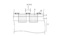
- An InP buffer layer 2 or InGaAs buffer layer 2 having a thickness of 2 ⁇ m is formed on the n-type InP substrate 1.
- the light receiving layer 3 having a multiple quantum well structure of (InGaAs / GaAsSb) or (GaInNAs / GaAsSb) is formed.
- the thickness of the GaInNAs layer or GaAsSb layer forming the unit quantum well structure is 5 nm, and the number of pairs (the number of repetitions of the unit quantum well) is 300.
- an InGaAs layer having a thickness of 1 ⁇ m is epitaxially grown on the light receiving layer 3 as a diffusion concentration distribution adjusting layer 4 at the time of introducing Zn diffusion, and finally, an InP window layer 5 having a thickness of 1 ⁇ m is epitaxially grown.
- Both the light receiving layer 3 and the diffusion concentration distribution adjusting layer 4 are preferably epitaxially grown by MBE (Molecular Beam Epitaxy) method.
- the InP window layer 5 may be epitaxially grown by the MBE method, or after the diffusion concentration distribution adjusting layer 4 is grown, the InP window layer 5 is taken out from the MBE apparatus and epitaxially grown by the MOVPE (Metal Organic Vapor Phase Epitaxy) method. Good.
- the InP buffer layer 2 or InGaAs buffer layer 2 may be non-doped, or may be doped with an n-type dopant such as Si by about 1E17 cm ⁇ 3 .
- the (InGaAs / GaAsSb) or (GaInNAs / GaAsSb) multi-quantum well structure light-receiving layer 3, InGaAs diffusion concentration distribution adjusting layer 4, and InP window layer 5 are preferably non-doped, but a very small amount of n-type dopant such as Si is used. Doping may be performed (for example, about 2E15 cm ⁇ 3 ).
- a high-concentration n-side electrode forming layer for forming an n-side electrode doped with about 1E18 cm ⁇ 3 of an n-type dopant may be inserted between the InP substrate 1 and the buffer layer 2.
- the InP substrate 1 may be a Fe-doped semi-insulating InP substrate.
- an n-side electrode may be formed by inserting an n-side electrode forming layer doped with n-type dopant about 1E18 cm ⁇ 3 between the semi-insulating InP substrate 1 and the buffer layer 2.
- An optical device is manufactured using a laminated structure (epitaxial wafer) including the InP substrate 1 described above.
- a laminated structure epiaxial wafer
- SiN mask pattern 36 formed on the surface 5 a of the InP window layer 5 Zn is selectively diffused from the opening, and the inside of the light-receiving layer 3 having the (InGaAs / GaAsSb) or (GaInNAs / GaAsSb) multiple quantum well structure
- the p-type region 6 is formed to reach The front tip of the p-type region 6 forms a pn junction 15.
- a high concentration region having a Zn concentration of about 1E18 cm ⁇ 3 or more is limited to the InGaAs diffusion concentration distribution adjusting layer 4.
- the high-concentration impurity distribution continues from the surface 5a of the InP window layer 5 in the depth direction to the InGaAs diffusion concentration distribution adjustment layer 4, and further 5E16 cm ⁇ at a deeper position in the diffusion concentration distribution adjustment layer 4. Decrease to 3 or less.
- the Zn concentration distribution in the vicinity of the pn junction 15 is a distribution indicating an inclined junction.
- the one-dimensional or two-dimensional array of the light-receiving elements 10, that is, the light-receiving element array 50 shown in FIG. 3 has a planar diffusion so as to be selectively diffused inside the peripheral edge of the light-receiving element without performing mesa etching for element separation.
- the adjacent light receiving elements are separated from each other by diffusion limited to the periphery. That is, the Zn selective diffusion region 6 is a main part of one light receiving element 10 and forms one pixel, but a region where Zn is not diffused separates each pixel. For this reason, it is possible to suppress dark current without being damaged by crystals accompanying the mesa etching.
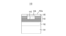
- FIG. 4 is a cross-sectional view showing a light receiving element 110 in Reference Example 1 different from the present invention.
- the light receiving element 110 of Reference Example 1 has the following laminated structure. (InP substrate 101 / InP or InGaAs buffer layer 102 / (GaInNAs / GaAsSb) light-receiving layer 103 / InP window layer 105 having a multiple quantum well structure)
- the difference is that there is no diffusion concentration distribution adjustment layer as compared with the laminated structure in the embodiment of the present invention. That is, the light receiving layer 103 having a multiple quantum well structure is disposed immediately below the InP window layer 105.
- the Zn concentration distribution has a high concentration up to the light receiving layer 103 having a multiple quantum well structure. Namely, within the multi-quantum well structure, a high impurity concentration regions 1E18 cm -3 is formed beyond 5E16 cm -3. When high concentration impurities are introduced into the multiple quantum well structure, the structure is destroyed and the dark current is greatly increased. Conversely, in order to prevent such a high concentration impurity region from being formed in the multiple quantum well structure, a diffusion concentration distribution adjusting layer is provided to perform selective diffusion of impurities.
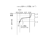
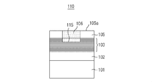
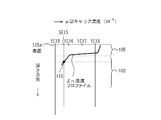
- FIG. 6 is a cross-sectional view showing the light receiving element 110 in Reference Example 2 for studying the cases (1) and (2).
- the light receiving element 110 of the reference example 2 has substantially the same laminated structure as the light receiving element of the reference example 1, but the thickness of the InP window layer 105 is larger than that of the reference example 1, and corresponds to the case of (2) above. To do. However, it is possible to consider the case of (1) at the same time.
- the Zn concentration distribution shown in FIG. 7 is obtained as a result of selective diffusion so as not to form a high concentration region of Zn in the multiple quantum well structure of the light receiving layer 103.
- the Zn concentration sharply decreases from the high concentration to the low concentration in the InP window layer 105, and is about 1E16 cm ⁇ 3 in the InP window layer 105 on the light receiving layer 103 side.
- a low concentration impurity region is formed.
- a low-concentration impurity region of about 1E16 cm ⁇ 3 is formed in the InP window layer 105, the electrical resistance increases in that region as described repeatedly, and the response speed decreases. For this reason, a material having a band gap energy that is large enough to form a window layer, specifically, the InP window layer 105 that is a typical material of the material cannot play a role of a diffusion concentration distribution adjusting layer. This is the same for the cases (1) and (2). Therefore, a material satisfying a band gap energy equal to or lower than InP, specifically, less than 1.34 eV, is preferably used for the diffusion concentration distribution adjustment layer. That is, even in a low concentration impurity region, it is necessary to use a material such as InGaAs in which the decrease in electrical conductivity is relatively small and the increase in electrical resistance is relatively small.
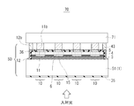
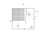
- FIG. 8 is a diagram showing an outline of the imaging apparatus according to Embodiment 2 of the present invention. Optical parts such as lenses are omitted.
- FIG. 9 is a diagram for explaining a light receiving element array of the imaging apparatus.
- FIG. 10 is a diagram showing one light receiving element in the light receiving element array 50 of FIG. 9.
- CMOS multiplexer
- the p-side electrode 11 electrically connected to the p-type region 6 of the epitaxial layer of each light receiving element 10 and the n-side electrode 12 provided on the common n-type InP substrate 51 (1) are connected to the multiplexer 71.
- the p-side electrode 11 and the n-side electrode 12 send an electrical signal to the multiplexer, and the multiplexer 71 receives the electrical signal from each light receiving element 10 and performs a process of forming an entire image of the object.
- the n-side electrode 12 and the p-side electrode 11 are electrically connected to the multiplexer 71 via solder bumps 12b and 11b, respectively.
- Incident light is introduced through an AR (Anti-Reflection) film 35 formed on the back surface of the InP substrate 51, and is received by a pn junction 15 that is an interface between the p-type region 6 and the light-receiving layer 3.
- the p-type region 6 is formed by introducing Zn from an opening of a Zn selective diffusion mask pattern 36 of SiN that also serves as a protective film.
- the Zn diffusion mask pattern 36 is left as it is together with the protective polyimide film pattern 43 formed thereon.
- the light receiving elements 10 of the light receiving element array 50 are provided on a common InP substrate 51 (1).
- the current signal generated by receiving the cosmic light in the SWIR band by each light receiving element is sent to the multiplexer 71 that also serves as a mounting board as described above, and image forming processing is performed.
- the number of pixels is changed while changing the size and pitch of each light receiving element and the size of the array.
- the light receiving element array 50 shown in FIG. 9 has 90,000 pixels.
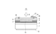
- the light receiving element 10 shown in FIG. 10 has a plurality of epitaxial films formed on the InP substrate 1, and a p-type impurity introduction diffusion mask 36 used for forming the p-type region 6 is provided. I'm leaving.
- a p-type electrode 11 is connected to the p-type region 6, and the p-type electrode 11 is connected to a wiring of a mounting substrate such as a multiplexer 71 by a solder bump or the like.
- FIG. 11 is a cross-sectional view for explaining an epi-up mounted light receiving element 10.
- the light receiving element in the imaging apparatus may be either epi-down mounting or epi-up mounting.
- the light receiving element 10 is formed on an n-type InP substrate 1 in order from the bottom: n-type InP buffer layer 2 / light-receiving layer 3 / diffusion concentration distribution adjusting layer 4 / InP window layer 5 / selective diffusion mask pattern 36 / antireflection film. (AR film: Anti-Reflection) 35 is located.
- the p-type region 6 is formed from the InP window layer 5 to the pn junction 15 in the light receiving layer 3 through the diffusion concentration distribution adjusting layer 4.
- the n-side electrode 12 is located on the back surface of the n-type InP substrate 1, and the p-side electrode 11 is located on the surface of the InP window layer 5 in the p-type region 6 and is electrically connected to the wiring electrode 27.
- the light receiving layer 3 receives light in the wavelength range of 1.0 ⁇ m to 3.0 ⁇ m.
- the light receiving layer 3 is formed by the above-described type II multiple quantum well structure.
- the light receiving element 10 shown in FIG. 11 is epi-up mounted as described above, and light is incident from the epitaxial layer, that is, the InP window layer 5 side.
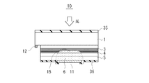
- the light receiving element in the present embodiment may be of a type that is epi-down mounted and that receives light from the back side of the n-type InP substrate 1 as shown in FIG.
- an AR film 35 is applied to the back surface of the InP substrate 1.
- the selective diffusion mask pattern 36 of SiN also serving as the diffusion concentration distribution adjusting layer 4, the InP window layer 5, the p-side electrode 11 and the protective film is provided in the same manner as in the case of epi-up mounting.
- the SWIR band light reaches the pn junction 15 of the light receiving layer 3 without being absorbed.
- the light receiving layer 3 is formed by the above-described type II multiple quantum well structure. This also applies to the following examples of the present invention unless otherwise specified.
- the p-side electrode 11 and the n-side electrode 12 may be arranged at positions facing each other with the n-type InP substrate 1 interposed therebetween as shown in FIG. 11, or the n-type InP substrate as shown in FIG. 1 may be arranged on the same side.
- each light receiving element 10 of the light receiving element array 50 shown in FIG. 9 and the integrated circuit are electrically connected by flip chip mounting.
- the light reaching the pn junction 15 is absorbed to generate a current signal, which is converted into an image of one pixel through the integrated circuit as described above.
- the n-type InP substrate 1 is preferably an off-angle substrate inclined from 5 to 20 degrees in the [111] direction or the [11-1] direction from (100). More preferably, the angle is inclined by 10 to 15 degrees from (100) to the [111] direction or the [11-1] direction.
- the n-type InP buffer layer 2, the type II quantum well structure light-receiving layer 3, the InGaAs diffusion concentration distribution adjusting layer 4 and the InP window layer having a small defect density and excellent crystallinity are used. 5 can be obtained. As a result, it is possible to obtain a light receiving layer in which dark current is suppressed and there are few dark spots.
- the action of the light receiving element formed using the off-angle substrate is particularly useful for improving the quality of an image pickup apparatus that receives and picks up space light.
- Such a large off-angle as described above has never been proposed for the InP substrate, and has been confirmed for the first time by the present inventors.
- the large off angle as described above is an important factor in growing a good crystalline epitaxial film on an InP substrate.
- a compound semiconductor containing N such as GaInNAs
- the light-receiving layer 3 having the above-described quantum well structure which is capable of emitting and receiving light in a very long wavelength region.
- an InP substrate having a large off-angle as described above it is actually impossible to form a good epitaxy layer that can withstand practical use.
- an InP substrate having a large off-angle as described above a compound semiconductor containing N, such as GaInNAs, suppresses dark current and does not become a light-receiving layer with reduced dark spots. As a result, a clear image cannot be obtained using weak SWIR band space light.
- the off-angle of the InP substrate is the same in GaInNAsP and GaInNAsSb in that a large angle range as described above is necessary to obtain good crystallinity.
- FIG. 11 and FIG. 12 includes an InGaAs diffusion concentration distribution adjusting layer 4 and an InP window layer 5 positioned so as to cover the light receiving layer 3. Since the lattice constant of the light receiving layer 3 is the same as the lattice constant of the n-type InP substrate 1, the InGaAs diffusion concentration distribution adjusting layer 4 and the InP window layer 5, which have a reputation for reducing the dark current, are formed on the light receiving layer 3. Can be formed. For this reason, dark current can be suppressed and element reliability can be improved. That is, in the conventional light receiving element, the lattice constant is increased from the InP substrate to InGaAs of the light receiving layer by providing the step buffer layer or the graded layer.
- the window layer needs to be an InAsP window layer having a composition matched to the lattice constant of the light receiving layer.
- the InAsP window layer having such a large lattice constant generally has poor absorption sensitivity due to absorption from the vicinity of the MWIR to the short wavelength side, resulting in a blurred image especially in an environment with a lot of moisture ( (See FIG. 27).
- InGaAs is used for the diffusion concentration distribution adjusting layer 4 and InP layer is used for the window layer. And dark current can be kept low.
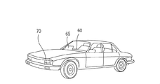
- FIG. 13 is a diagram showing a visual field support apparatus according to Embodiment 3 of the present invention.
- This visual field support device is mounted on a vehicle in order to support a driver's forward visual field when driving a car at night.
- the vehicle includes an imaging device 70 including the light-receiving element array described in the first and second embodiments and an optical element such as a lens (not shown), a display monitor 65 that displays a captured image, and drive-controls them.
- a control device 60 is mounted.
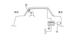
- FIG. 14 is a view assisting device mounted on a vehicle in order to assist the driver's rear view in driving a car at night.
- An image picked up by the image pickup device 70 including the light receiving element array of the second embodiment, an optical element such as a lens, and the like attached to the rear portion of the automobile rearward is displayed on the display device 65 in the upper front of the driver.
- the imaging device 70 and the display device 65 are driven and controlled by the control device 60.
- the conventional vehicle vision support device has the following problems because it receives reflected light or emitted light in the infrared region from an object to form an image.
- a light source When using reflected light, a light source is required, a mounting space is required, and the cost is increased.
- the radiant heat of an object it is difficult to recognize a pedestrian or the like wearing a non-heating element other than a person or a cold protection device, so it is necessary to use it together with a recognition means other than an infrared camera.
- a light source it is necessary to take measures against the human body, that is, eye-safe measures depending on the wavelength range to be used.
- the above extra light source and eye-safe measures are not necessary. Moreover, it does not matter whether the imaging target is heated or not. Furthermore, a clear image of the object can be obtained even in an environment containing moisture such as in fog. For this reason, the visual field assistance apparatus for vehicles excellent at night can be provided. This is because a light receiving element that utilizes the reflected light of the cosmic light in the SWIR band from the object, has a sufficiently low dark current, and has an excellent dynamic range (S / N).
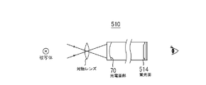
- FIG. 15 is a diagram showing a configuration of a night vision apparatus according to Embodiment 4 of the present invention.
- the night vision device 510 is characterized in that the imaging device 70 according to Embodiment 2 of the present invention or an imaging device in which the two-dimensional array surface of the light receiving elements thereof is deformed into a curved surface or the like is used for the imaging portion of the subject. Since the imaging device 70 has high light receiving sensitivity in the near infrared to infrared region and can suppress dark current, it is not necessary to incorporate a light source such as an infrared light emitting device in the night vision device. Further, as will be described later, it is possible to make an essential difference in the basic performance of the night vision device as compared with the conventional night vision device of the built-in infrared light source.
- the display surface may be a liquid crystal screen, for example, if it is a type that takes out current for each pixel on the photocathode and amplifies it with an amplification circuit, or displays it on the phosphor screen when it is amplified with an image intensifier. You can see through the eyepiece.
- the image intensifier is arranged behind the MCP, a microchannel plate MCP that doubles the electronic image converted by the photocathode, a fluorescent screen that is arranged behind the MCP, converts the electronic image back into an optical image, and is arranged behind the fluorescent screen. And a fiber plate that divides a subject image converted into an optical image into pixels and transmits the image.
- the photocathode 70 is formed by the two-dimensional array of the light receiving elements 10 or the imaging device described in the first embodiment, so that a light receiving layer having high sensitivity in the near infrared region is formed. Used.
- the night-vision apparatus can be suitably used particularly for observation of dynamics of an animal at night.
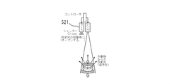
- FIG. 16 is a perspective view for explaining the nighttime navigation support apparatus 520 according to the fifth embodiment of the present invention.
- this nighttime navigation support apparatus 520 includes a radar apparatus including a radar antenna.
- the radar aerial is installed at a position with a good view on the ship, and is rotated in a horizontal plane by a control circuit (not shown) to capture a target such as another ship existing around.
- the radar indicator located in the hull is an indicator that displays a target captured by the radar antenna, and outputs a signal indicating the relative position of the target with respect to the ship.
- the camera 521 is installed at a predetermined position on the ship (a position at a predetermined distance from the radar antenna).
- the camera 521 is characterized in that the imaging device 70 including the light receiving layer 3 described in the second embodiment is incorporated.
- the camera 521 is mounted on, for example, a camera mount that includes a horizontal axis motor and a vertical axis motor, and its orientation can be controlled around the vertical axis and the horizontal axis.
- the camera 521 is activated when a target is captured by the radar indicator and this target is selected as a shooting target. Further, the horizontal axis and vertical axis motors included in the camera mount are driven so that the target can be continuously displayed on the display device that continues to capture the target by the camera 521.
- a target tracking calculator For such tracking shooting by the camera 521, a target tracking calculator is provided.
- the target tracking computing unit activates the camera 521 and starts driving control of a motor included in the camera mount, and causes the camera 521 to start tracking shooting of the target. .
- the camera 521 incorporates the imaging device 70 according to the second embodiment as described above, the near-infrared sensitivity is excellent, there is no need to use a temperature difference, and it is not affected by the sea surface temperature regardless of day or night. .
- the camera 521 has high sensitivity in a wavelength region that is not easily affected by water vapor, so that it is not easily affected by rain, fog, etc., and can capture a target clearly at night.
- FIG. 17 is an explanatory diagram of the principle of the laser radar that forms the core of the nighttime navigation support apparatus according to Embodiment 6 of the present invention.
- the laser radar in the present embodiment is characterized in that a camera incorporating the imaging device 70 shown in the second embodiment is arranged.
- a turning platform for turning the laser radar has a function of changing an elevation angle and turning, and is controlled by a control circuit.
- the laser radar on which the camera is arranged includes a laser head, a light transmission optical system, a light receiving zoom lens, a camera head, and the like.
- the laser head is composed of a semiconductor laser or the like that emits an invisible ultrashort pulse laser beam in the near-infrared wavelength band.
- the camera head includes a camera 521 for receiving the reflected pulsed laser beam.
- the pulsed laser light is emitted toward the target, and suspended particles such as rain and fog are present along the way.
- the shutter of the camera 521 is closed, so that the light reflected by the suspended particles such as rain and fog existing in front of the object is sent to the shutter. It is blocked and does not reach the camera 521.
- only the reflected light from the object at a specific distance is received by opening the shutter only when the light reaches the object and is reflected and the reflected light reaches the camera 521. can do.
- the distance to the object can be set by adjusting the timing of opening the shutter, and by using the highly sensitive camera 521, it can be used day or night, and it can be used for bad weather such as rain and fog and high waves. Even at this time, it is possible to significantly reduce these effects and observe only the object. In addition, non-ferrous objects, such as wooden or plastic small ships, and sea surface suspended objects can be clearly seen in shape.
- the imaging device 70 shown in the second embodiment is used in the camera 521 in combination with an image intensifier functional component. Therefore, for example, the wavelength range of the laser beam of the laser radar can be set to a near infrared region that is not easily affected by rain and fog, and a clearer image can be obtained.
- FIG. 18 is a diagram illustrating a train accident avoidance device 530 according to Embodiment 7 of the present invention.
- the feature of this embodiment is that the imaging device 70 described in Embodiment 2 is incorporated in the TV camera 531.
- this train accident avoidance device detects a TV camera 531 that monitors and monitors a predetermined range, an abnormality determination unit, and an obstacle that the TV camera 531 has entered the train track, and an accident occurs.
- a central monitoring device and an emergency information output unit for notifying the occurrence of an emergency situation are provided.
- One or a plurality of TV cameras 531 are provided so as to monitor a predetermined range, for example, a train track laid in the platform site over the entire length.
- the imaging area of the TV camera 531 in the case of installing one is a train track and a platform in front of the train.
- the above TV camera 531 incorporates the imaging device 70 shown in FIG. 8, so that a clear image can be obtained and in a wavelength range that is not easily affected by moisture even when there is rain or fog. Since it has high sensitivity, it can be reliably monitored regardless of the weather. Moreover, since it is not necessary to irradiate infrared rays or the like, the eye-safe problem can be avoided for a large number of passengers.
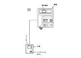
- FIG. 19 is a diagram showing a visitor monitoring device 540 according to the eighth embodiment of the present invention.
- the visitor monitoring device 540 includes a parent device and a child device of a camera-equipped doorphone.
- the child is provided at the door, and the visitor presses the button on the door chime and is photographed through the filter.
- the parent device is provided indoors, and an image of the visitor captured by the child device camera is displayed on the display screen of the parent device.
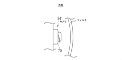
- FIG. 20 is a diagram showing the camera 541 provided in the slave unit.
- the camera 541 incorporates the imaging device 70 shown in FIG. 8 and images a visitor.
- the imaging device 70 having a light receiving layer having high sensitivity in the near-infrared region to the infrared region is used and a visitor can be identified by reflection of space light (night glow), for example, a conventional door phone with a camera
- space light night glow
- the eye-safe problem resulting from infrared irradiation can be avoided, and further, the power supply of a light source such as an infrared light emitting LED can be omitted. For this reason, the structure of the slave unit of the door phone with camera can be simplified, the power consumption can be reduced, and the eye-safe problem can be avoided. Moreover, since the natural light of the universe is constant day and night, it is possible to obtain a clear image of the visitor without a sense of incongruity due to the difference between day and night.
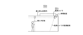
- FIG. 21 is a diagram illustrating an intruder detection device 550 according to the eighth embodiment of the present invention.
- the monitoring camera 551 is installed in the room so that the outside can be monitored through the transparent window surface.
- the monitoring camera 551 incorporates the imaging device 70 shown in FIG. 8 of Embodiment 2 and has high sensitivity in the near infrared to infrared range.
- the image is taken by the monitoring camera 551, the image is sent to the processing device, the person is detected by image processing, and the stagnation time near the window surface is measured, and it is determined that the possibility of intrusion is large for a specified time. In the case of a stagnation time of 1 minute or longer, it is determined that the person is an intruder.
- the surveillance camera 551 in the present embodiment is characterized in that an imaging device 70 having high sensitivity in the near infrared to infrared region is incorporated, so that it is not necessary to provide an infrared irradiator.
- the monitoring camera 551 can detect a person who is scheduled to enter with high discrimination power by receiving reflected light of a person's cosmic light (night glow). For this reason, the structure of this kind of monitoring apparatus can be simplified.
- the intruder monitoring device concentrates infrared irradiation particularly on the person to be photographed, it is possible to avoid troubles that are likely to be problematic.
- the conventional monitoring device different from the above type requires the arrangement of an infrared LED as a light source.
- a substrate is arranged so that the facing angle with the front can be freely changed by driving a motor, and a plurality of light emitting LEDs are mounted on the substrate.
- the monitoring range is irradiated with infrared rays from the light emitting LED, and the monitoring camera receives the reflected light and images it.
- the surveillance camera lens is changed from standard to wide angle, or from wide angle to standard, or when the surveillance area is changed, the luminance data of the video signal from the surveillance camera is obtained, the luminance distribution is obtained, and the luminance distribution is detected.
- the motor is driven to change the facing angle of the substrate to change the irradiation angle of the light emitting LED so that the luminance distribution becomes uniform.
- the monitoring camera 551 in the modification of the present embodiment shown in FIG. 22 uses the imaging device 70 having high sensitivity in the near infrared to infrared region, and is used for the monitoring device to monitor a dark place.
- clear imaging can be performed without a light emitting LED, and the luminance distribution can be accurately detected.
- the reflected light of the cosmic light night glow
- FIG. 23 is a diagram for explaining an indoor monitoring apparatus 560 according to Embodiment 10 of the present invention.
- the monitoring camera 561 incorporates the imaging device 70 shown in FIG. 8 and is arranged so as to image the interior of the home.
- the sensor terminal is formed integrally with the above-described monitoring camera, and is configured to determine the presence of a person by processing an image captured by the monitoring camera and calculating a human presence probability or the like. .
- the sensor terminal determination result is notified to the home terminal via the LAN, and is notified from the home terminal to the center terminal of the center via the telephone line.
- an artificial retinal camera or the like may be used as the monitoring camera 561.
- infrared cameras it is necessary to always irradiate the entire living space of indoor residents (caregivers) with infrared lamps, and the effects of infrared light irradiation on the caregivers cannot be ignored. It was.
- the care receiver's facial expression and motion are unclear at the position where the irradiation is shadowed, and the response may be delayed.
- the monitoring camera 561 has a high light receiving sensitivity in the near infrared to infrared region, and therefore can perform high-sensitivity imaging in the dark and under illumination without irradiating with infrared light, and the above-described human existence probability Can be calculated with high accuracy, and the delay in correspondence can be eliminated.
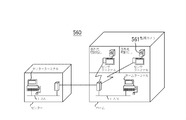
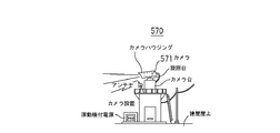
- FIG. 24 is a diagram for explaining a monitoring device for urban disaster prevention in Embodiment 11 of the present invention.
- This urban disaster prevention monitoring device 570 can automatically detect a fire and can easily identify the location of the fire.
- a camera stand is provided on the roof of a building, and the monitoring camera 571 is housed in a camera housing attached to the upper turntable.
- the surveillance camera 571 in the present embodiment is characterized in that the imaging device 70 shown in FIG. 8 is incorporated. For this reason, infrared light emitted from a fire or the like can be detected with high sensitivity.
- an infrared image of a predetermined area in the city is captured by changing the imaging direction of the surveillance camera 571 by driving a swivel on which the surveillance camera is mounted, and monitoring the angle at that time. can do. If the image signal is arithmetically processed to recognize a local heat source, the fire occurrence site can be detected. By plotting the imaging direction of the monitoring camera 571 at that time on the coordinate axis superimposed on the overhead view using the monitoring device, it is possible to accurately determine the location of the fire occurrence.
- another conventional urban disaster prevention monitoring device uses a monitoring camera that visualizes the infrared radiation of the flame as a fire detection sensor, and performs image processing on a near-infrared image captured by the monitoring camera.
- the fire detection device reliably detected the fire at an early stage and identified the location of the fire.
- the imaging device 70 shown in FIG. 8 is incorporated in the monitoring camera that images the radiation infrared rays of the flame. .
- image processing is performed on a near-infrared image captured by a monitoring camera in another urban disaster prevention monitoring apparatus according to the eleventh embodiment, so that it is reliably detected at an early stage of the fire without being influenced by the weather or the like. And the location of the fire can be identified. Furthermore, by adding the function of the fire determination device, it is possible to check the fire situation using a near-infrared image and obtain highly accurate temperature information.
- FIG. 25 is a diagram for explaining a remote monitoring device 580 according to the twelfth embodiment of the present invention.
- This remote monitoring system 580 eliminates the need for electric wiring when monitoring day and night. Also, no night lighting is required during night monitoring.
- the present embodiment is characterized in that an imaging device 70 shown in FIG.
- a phosphorescent material or the like at the location to be monitored, and the equipment to be monitored is not particularly limited and may be anything. Examples include drainage holes in sabo dams, dam water level and sedimentation level display lines, factory equipment, houses, buildings, padlocks on shelves in controlled areas, and observation equipment installed in the mountains.
- the material cost of the phosphorescent material, the initial arrangement thereof, and the number of man-hours for renewal associated with aged deterioration can be omitted.
- positioned over a wide range can be solved. That is, an intruder from a route that does not place the phosphorescent material and the surrounding situation during heavy rain cannot be grasped even if the phosphorescent material is locally arranged, but when using the monitoring camera 581 equipped with the imaging device 70, the near red Since it has high light receiving sensitivity in the outer to infrared region, a clear image can be obtained without using an infrared light emitting device. Further, an infrared projector (infrared light emitting device) is naturally unnecessary. As a result, simplification, miniaturization, cost saving, etc. of the apparatus can be realized.
- the imaging device has light receiving sensitivity up to about 3 ⁇ m on the long wavelength side.
- the SWIR cosmic light has an intensity distribution shown in FIG. From FIG. 26, the imaging apparatus according to the embodiment of the present invention can cover the entire area of SWIR space light.
- FIG. 27 shows the absorption spectrum of water.
- the image pickup apparatus can avoid the influence of water absorption by providing a light receiving sensitivity limited to 1 ⁇ m to 2 ⁇ m by applying a filter, for example. As a result, a clear image can be obtained without the influence of rain, fog, etc., for example.
- the light receiving element interval or the pixel pitch is the width of the non-opening portion of the SiN selective diffusion mask pattern 36 as shown in FIG.
- the p-side electrode 11 was formed of AuZn
- the n-side electrode 12 was formed of AuGeNi.
- the n-side electrode 12 is provided on the high concentration impurity buffer layer 2.
- an n-side electrode 11 may be provided on the back surface of the substrate, or an n-type semiconductor layer (for example, buffer layer 2) adjacent to the substrate on the substrate surface side.
- An n-side electrode may be provided.
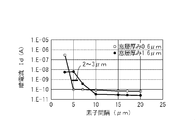
- a dark current was measured by applying a reverse bias voltage of 5 V between the p-side electrode 11 and the n-side electrode 12 of the light receiving element array of FIG.
- the InP window layer 5 has a thickness of 0.6 ⁇ m and 1.6 ⁇ m, and an element interval of 7 types over a range of 3 ⁇ m to 20 ⁇ m. .
- the thickness of the diffusion concentration distribution adjusting layer 4 was 1 ⁇ m.
- Results are shown in FIG. According to FIG. 29, when the thickness of the InP window layer 5 is as thin as 0.6 ⁇ m, the dark current can be 1E-10 A (ampere) even if the element interval or pixel pitch is reduced to 5 ⁇ m.
- the thickness of the InP window layer 5 is 1.6 ⁇ m, as described above, the diffusion of Zn in the lateral direction spreads, and 1E-10A cannot be achieved unless the element spacing exceeds 7 ⁇ m.
- the element spacing could be 5 ⁇ m by reducing the thickness of the InP window layer 5 to 0.6 ⁇ m and disposing the diffusion concentration distribution adjusting layer.
- FIG. 30 shows the concentration distribution of Zn in the depth direction.
- the peak value of Zn pileup is suppressed to 5 ⁇ 10 16 cm ⁇ 3 or less at the interface between the InGaAs diffusion concentration distribution adjusting layer 4 and the light receiving layer 3.
- the Zn concentration can be surely lowered, crystallinity, etc. Can be prevented.
- the arrangement of the diffusion concentration distribution adjusting layer 4 allows the multiple quantum well structure of the light receiving layer to have its original function.
- the light receiving element or the light receiving element array provided with the diffusion concentration distribution adjusting layer has been described, but most widely, the light receiving element does not include the diffusion concentration distribution adjusting layer. It is only necessary that the impurity concentration is 5E16 cm ⁇ 3 or less and the impurity is introduced by selective diffusion.
- the imaging device for receiving and imaging the cosmic light can be made of any material as long as each light receiving element is formed of a light receiving layer having a quantum well structure having a sensitivity of 3.0 ⁇ m or less. It may be configured. Moreover, although the visual field assistance apparatus of this invention demonstrated the visual field assistance apparatus for motor vehicles, you may use it for uses other than motor vehicles, such as a medical use and a biometric recognition.
- a light receiving element that has light receiving sensitivity in the near infrared region, can easily obtain good crystallinity, can easily form a one-dimensional or two-dimensional array with high accuracy, and can reduce dark current, A light receiving element array in which the light receiving elements are arranged can be obtained.
- the imaging device and the visual field support device of the present invention can receive the entire area of the cosmic light using the cosmic light in the SWIR band as a light source, and do not receive light in an unnecessarily wide band as the dark current increases. Therefore, dark current and dark spots can be suppressed, clear imaging can be performed, and it is possible to contribute to reduction of mounting space and manufacturing cost.
- an InP window layer can be used, and it has a good sensitivity over the entire space light, and it is possible to obtain a clear image by suppressing the dark current lower.
Landscapes
- Chemical & Material Sciences (AREA)
- Engineering & Computer Science (AREA)
- Nanotechnology (AREA)
- Physics & Mathematics (AREA)
- Life Sciences & Earth Sciences (AREA)
- Biophysics (AREA)
- Optics & Photonics (AREA)
- Crystallography & Structural Chemistry (AREA)
- Light Receiving Elements (AREA)
- Traffic Control Systems (AREA)
- Alarm Systems (AREA)
Priority Applications (3)
| Application Number | Priority Date | Filing Date | Title |
|---|---|---|---|
| EP09812961.2A EP2328187B1 (en) | 2008-09-11 | 2009-07-24 | Image pickup device, visibility support apparatus, night vision device, navigation support apparatus, and monitoring device |
| US13/063,444 US8243139B2 (en) | 2008-09-11 | 2009-07-24 | Image pickup device, visibility support apparatus, night vision device, navigation support apparatus, and monitoring device |
| US13/548,668 US8564666B2 (en) | 2008-09-11 | 2012-07-13 | Image pickup device, visibility support apparatus, night vision device, navigation support apparatus, and monitoring device |
Applications Claiming Priority (2)
| Application Number | Priority Date | Filing Date | Title |
|---|---|---|---|
| JP2008-233948 | 2008-09-11 | ||
| JP2008233948A JP5233535B2 (ja) | 2008-09-11 | 2008-09-11 | 撮像装置、視界支援装置、暗視装置、航海支援装置および監視装置 |
Related Child Applications (2)
| Application Number | Title | Priority Date | Filing Date |
|---|---|---|---|
| US13/063,444 A-371-Of-International US8243139B2 (en) | 2008-09-11 | 2009-07-24 | Image pickup device, visibility support apparatus, night vision device, navigation support apparatus, and monitoring device |
| US13/548,668 Continuation US8564666B2 (en) | 2008-09-11 | 2012-07-13 | Image pickup device, visibility support apparatus, night vision device, navigation support apparatus, and monitoring device |
Publications (1)
| Publication Number | Publication Date |
|---|---|
| WO2010029813A1 true WO2010029813A1 (ja) | 2010-03-18 |
Family
ID=42005074
Family Applications (1)
| Application Number | Title | Priority Date | Filing Date |
|---|---|---|---|
| PCT/JP2009/063246 Ceased WO2010029813A1 (ja) | 2008-09-11 | 2009-07-24 | 撮像装置、視界支援装置、暗視装置、航海支援装置および監視装置 |
Country Status (4)
| Country | Link |
|---|---|
| US (2) | US8243139B2 (enExample) |
| EP (1) | EP2328187B1 (enExample) |
| JP (1) | JP5233535B2 (enExample) |
| WO (1) | WO2010029813A1 (enExample) |
Cited By (2)
| Publication number | Priority date | Publication date | Assignee | Title |
|---|---|---|---|---|
| WO2012002144A1 (ja) * | 2010-06-29 | 2012-01-05 | 住友電気工業株式会社 | 受光素子およびその製造方法 |
| US8188559B2 (en) | 2008-02-01 | 2012-05-29 | Sumitomo Electric Industries, Ltd. | Light-receiving element and light-receiving element array |
Families Citing this family (20)
| Publication number | Priority date | Publication date | Assignee | Title |
|---|---|---|---|---|
| JP5498662B2 (ja) * | 2008-03-26 | 2014-05-21 | 国立大学法人 東京大学 | 半導体装置および半導体装置の製造方法 |
| JP4743453B2 (ja) * | 2008-12-25 | 2011-08-10 | 住友電気工業株式会社 | 気体モニタリング装置、燃焼状態モニタリング装置、経年変化モニタリング装置、および不純物濃度モニタリング装置 |
| CN102498327B (zh) * | 2009-06-15 | 2015-09-23 | 夏普株式会社 | 发光模块、照明装置、显示装置以及电视接收装置 |
| JP5218476B2 (ja) * | 2010-06-03 | 2013-06-26 | 住友電気工業株式会社 | 半導体素子、光学センサ装置および半導体素子の製造方法 |
| JP5748176B2 (ja) * | 2011-11-01 | 2015-07-15 | 住友電気工業株式会社 | 受光素子、エピタキシャルウエハおよびその製造方法 |
| EP2713409B1 (en) * | 2012-09-27 | 2020-08-26 | ams AG | Photodiode with a field electrode for reducing the space charge region |
| US20140217540A1 (en) * | 2013-02-04 | 2014-08-07 | Teledyne Scientific & Imaging, Llc | Fully depleted diode passivation active passivation architecture |
| JP6454981B2 (ja) * | 2014-04-24 | 2019-01-23 | 住友電気工業株式会社 | 半導体積層体および受光素子 |
| JP6877815B2 (ja) * | 2014-10-17 | 2021-05-26 | 日本無線株式会社 | 画像生成装置 |
| JP6609331B2 (ja) * | 2015-07-07 | 2019-11-20 | ビー.ジー. ネゲヴ テクノロジーズ アンド アプリケーションズ リミテッド、アット ベン−グリオン ユニヴァーシティ | Swirを目に見えるものへとアップコンバージョンする光学系 |
| JP2018190798A (ja) * | 2017-04-28 | 2018-11-29 | 住友電気工業株式会社 | 赤外線検知半導体デバイス |
| US10304881B1 (en) | 2017-12-15 | 2019-05-28 | Atomera Incorporated | CMOS image sensor with buried superlattice layer to reduce crosstalk |
| US10276625B1 (en) * | 2017-12-15 | 2019-04-30 | Atomera Incorporated | CMOS image sensor including superlattice to enhance infrared light absorption |
| US10361243B2 (en) | 2017-12-15 | 2019-07-23 | Atomera Incorporated | Method for making CMOS image sensor including superlattice to enhance infrared light absorption |
| US10461118B2 (en) | 2017-12-15 | 2019-10-29 | Atomera Incorporated | Method for making CMOS image sensor including photodiodes with overlying superlattices to reduce crosstalk |
| US10355151B2 (en) | 2017-12-15 | 2019-07-16 | Atomera Incorporated | CMOS image sensor including photodiodes with overlying superlattices to reduce crosstalk |
| US10396223B2 (en) | 2017-12-15 | 2019-08-27 | Atomera Incorporated | Method for making CMOS image sensor with buried superlattice layer to reduce crosstalk |
| US11101119B2 (en) | 2018-12-20 | 2021-08-24 | Elbit Systems Of America, Llc | Usage and temperature compensation of performance parameters for night vision device |
| US11641003B2 (en) * | 2019-12-03 | 2023-05-02 | Northwestern University | Methods of fabricating planar infrared photodetectors |
| TWI832715B (zh) * | 2023-03-02 | 2024-02-11 | 聯亞光電工業股份有限公司 | 半導體元件 |
Citations (15)
| Publication number | Priority date | Publication date | Assignee | Title |
|---|---|---|---|---|
| JPS631079A (ja) * | 1986-06-20 | 1988-01-06 | Hitachi Ltd | 半導体受光素子およびその製造方法 |
| JPH0338887A (ja) * | 1989-07-06 | 1991-02-19 | Fujitsu Ltd | 半導体受光素子 |
| JPH05160426A (ja) * | 1991-12-06 | 1993-06-25 | Nec Corp | 半導体受光素子 |
| JPH05160429A (ja) * | 1991-12-09 | 1993-06-25 | Nec Corp | 赤外線検知器 |
| JPH07302928A (ja) | 1994-05-09 | 1995-11-14 | Mitsubishi Electric Corp | 半導体受光素子ならびに半導体受光素子アレイおよび画像処理装置ならびに画像処理方法 |
| JPH0937147A (ja) | 1995-07-19 | 1997-02-07 | Honda Motor Co Ltd | 視覚装置 |
| JPH09219563A (ja) | 1996-02-09 | 1997-08-19 | Hitachi Ltd | 半導体光素子とそれを用いた応用システム |
| JP2001144278A (ja) | 1999-11-12 | 2001-05-25 | Nippon Sheet Glass Co Ltd | 受光素子アレイ |
| JP2002274258A (ja) | 2001-03-23 | 2002-09-25 | Stanley Electric Co Ltd | 自動車用暗視システム |
| JP2004350228A (ja) | 2003-05-26 | 2004-12-09 | Denso Corp | 車両用夜間後方視界支援システム |
| JP2007080920A (ja) * | 2005-09-12 | 2007-03-29 | Mitsubishi Electric Corp | アバランシェフォトダイオード |
| JP2007201432A (ja) * | 2005-12-28 | 2007-08-09 | Sumitomo Electric Ind Ltd | 撮像装置、視界支援装置、暗視装置、航海支援装置および監視装置 |
| JP2008153311A (ja) * | 2006-12-14 | 2008-07-03 | Sumitomo Electric Ind Ltd | 半導体受光素子、視界支援装置および生体医療装置 |
| JP2008171885A (ja) * | 2007-01-09 | 2008-07-24 | Sumitomo Electric Ind Ltd | 半導体受光素子およびその製造方法 |
| JP2008205001A (ja) * | 2007-02-16 | 2008-09-04 | Sumitomo Electric Ind Ltd | 受光素子、センサおよび撮像装置 |
Family Cites Families (8)
| Publication number | Priority date | Publication date | Assignee | Title |
|---|---|---|---|---|
| JP5008874B2 (ja) | 2005-02-23 | 2012-08-22 | 住友電気工業株式会社 | 受光素子と受光素子を用いた光通信用受信モジュールおよび受光素子を用いた計測器 |
| US7679059B2 (en) | 2006-04-19 | 2010-03-16 | Spectrasensors, Inc. | Measuring water vapor in hydrocarbons |
| JP2007324572A (ja) | 2006-05-02 | 2007-12-13 | Sumitomo Electric Ind Ltd | 受光素子アレイ、その製造方法、および光計測システム |
| US7608825B2 (en) * | 2006-12-14 | 2009-10-27 | Sumitomo Electric Industries, Ltd. | Image pickup device, vision enhancement apparatus, night-vision apparatus, navigation support apparatus, and monitoring apparatus |
| JP5515162B2 (ja) * | 2007-03-23 | 2014-06-11 | 住友電気工業株式会社 | 半導体ウエハの製造方法 |
| JP2008288293A (ja) | 2007-05-16 | 2008-11-27 | Nippon Telegr & Teleph Corp <Ntt> | 半導体受光素子 |
| JP5195172B2 (ja) * | 2008-08-29 | 2013-05-08 | 住友電気工業株式会社 | 水分検出装置、生体中水分検出装置、自然産物中水分検出装置、および製品・材料中水分検出装置 |
| JP5233549B2 (ja) * | 2008-09-22 | 2013-07-10 | 住友電気工業株式会社 | 食品品質検査装置、食品成分検査装置、異物成分検査装置、食味検査装置および変移状態検査装置 |
-
2008
- 2008-09-11 JP JP2008233948A patent/JP5233535B2/ja not_active Expired - Fee Related
-
2009
- 2009-07-24 WO PCT/JP2009/063246 patent/WO2010029813A1/ja not_active Ceased
- 2009-07-24 EP EP09812961.2A patent/EP2328187B1/en not_active Not-in-force
- 2009-07-24 US US13/063,444 patent/US8243139B2/en active Active
-
2012
- 2012-07-13 US US13/548,668 patent/US8564666B2/en active Active
Patent Citations (15)
| Publication number | Priority date | Publication date | Assignee | Title |
|---|---|---|---|---|
| JPS631079A (ja) * | 1986-06-20 | 1988-01-06 | Hitachi Ltd | 半導体受光素子およびその製造方法 |
| JPH0338887A (ja) * | 1989-07-06 | 1991-02-19 | Fujitsu Ltd | 半導体受光素子 |
| JPH05160426A (ja) * | 1991-12-06 | 1993-06-25 | Nec Corp | 半導体受光素子 |
| JPH05160429A (ja) * | 1991-12-09 | 1993-06-25 | Nec Corp | 赤外線検知器 |
| JPH07302928A (ja) | 1994-05-09 | 1995-11-14 | Mitsubishi Electric Corp | 半導体受光素子ならびに半導体受光素子アレイおよび画像処理装置ならびに画像処理方法 |
| JPH0937147A (ja) | 1995-07-19 | 1997-02-07 | Honda Motor Co Ltd | 視覚装置 |
| JPH09219563A (ja) | 1996-02-09 | 1997-08-19 | Hitachi Ltd | 半導体光素子とそれを用いた応用システム |
| JP2001144278A (ja) | 1999-11-12 | 2001-05-25 | Nippon Sheet Glass Co Ltd | 受光素子アレイ |
| JP2002274258A (ja) | 2001-03-23 | 2002-09-25 | Stanley Electric Co Ltd | 自動車用暗視システム |
| JP2004350228A (ja) | 2003-05-26 | 2004-12-09 | Denso Corp | 車両用夜間後方視界支援システム |
| JP2007080920A (ja) * | 2005-09-12 | 2007-03-29 | Mitsubishi Electric Corp | アバランシェフォトダイオード |
| JP2007201432A (ja) * | 2005-12-28 | 2007-08-09 | Sumitomo Electric Ind Ltd | 撮像装置、視界支援装置、暗視装置、航海支援装置および監視装置 |
| JP2008153311A (ja) * | 2006-12-14 | 2008-07-03 | Sumitomo Electric Ind Ltd | 半導体受光素子、視界支援装置および生体医療装置 |
| JP2008171885A (ja) * | 2007-01-09 | 2008-07-24 | Sumitomo Electric Ind Ltd | 半導体受光素子およびその製造方法 |
| JP2008205001A (ja) * | 2007-02-16 | 2008-09-04 | Sumitomo Electric Ind Ltd | 受光素子、センサおよび撮像装置 |
Non-Patent Citations (6)
| Title |
|---|
| A.YAMAMOTO ET AL.: "Optical properties of GaAs0.5Sb0.5 and In0.53Ga0.47As/GaAs0.5Sb0.5 type II single hetero-structures lattice-matched to InP substrates grown by molecular beam epitaxy", JOURNAL OF CRYSTAL GROWTH, vol. 201, no. 202, 1999, pages 872 - 876, XP004175256 * |
| MARSHALL J. COHEN: "Near-IR imaging cameras operate at room temperature", LASER FOCUS WORLD, June 1993 (1993-06-01), pages 109 |
| R. SIDHU: "A Long-Wavelength Photodiode on InP Using Lattice-Matched GaInAs-GaAsSb Type-II Quantum Wells", IEEE PHOTONICS TECHNOLOGY LETTERS, vol. 17, no. 12, 2005, pages 2715 - 2717, XP008146947, DOI: doi:10.1109/LPT.2005.859163 |
| See also references of EP2328187A4 |
| T. MURAKAMI; H. TAKAHASHI; M. NAKAYAMA; Y. MIURA; K. TAKEMOTO; D. HARA: "InxGal-xAs/InAsyPl-y detector for near infrared (1-2.6 pm)", CONFERENCE PROCEEDINGS OF INDIUM PHOSPHIDE AND RELATED MATERIALS, May 1995 (1995-05-01), pages 528 - 531 |
| VATSIA, MIRSHRI, L.: "Atmospheric Optical Environment", RESEARCH AND DEVELOPMENT TECHNICAL REPORT ECOM-7023, September 1972 (1972-09-01) |
Cited By (5)
| Publication number | Priority date | Publication date | Assignee | Title |
|---|---|---|---|---|
| US8188559B2 (en) | 2008-02-01 | 2012-05-29 | Sumitomo Electric Industries, Ltd. | Light-receiving element and light-receiving element array |
| US8729527B2 (en) | 2008-02-01 | 2014-05-20 | Sumitomo Electric Industries, Ltd. | Light-receiving element, light-receiving element array, method for manufacturing light-receiving element and method for manufacturing light-receiving element array |
| WO2012002144A1 (ja) * | 2010-06-29 | 2012-01-05 | 住友電気工業株式会社 | 受光素子およびその製造方法 |
| JP2012015170A (ja) * | 2010-06-29 | 2012-01-19 | Sumitomo Electric Ind Ltd | 受光素子およびその製造方法 |
| US8822977B2 (en) | 2010-06-29 | 2014-09-02 | Sumitomo Electric Industries, Ltd. | Photodetector and method of manufacturing the photodetector |
Also Published As
| Publication number | Publication date |
|---|---|
| US8243139B2 (en) | 2012-08-14 |
| EP2328187B1 (en) | 2016-11-16 |
| US20120274771A1 (en) | 2012-11-01 |
| JP5233535B2 (ja) | 2013-07-10 |
| US20110164136A1 (en) | 2011-07-07 |
| EP2328187A1 (en) | 2011-06-01 |
| US8564666B2 (en) | 2013-10-22 |
| JP2010067861A (ja) | 2010-03-25 |
| EP2328187A4 (en) | 2014-08-06 |
Similar Documents
| Publication | Publication Date | Title |
|---|---|---|
| JP5233535B2 (ja) | 撮像装置、視界支援装置、暗視装置、航海支援装置および監視装置 | |
| JP2010067861A5 (enExample) | ||
| US7608825B2 (en) | Image pickup device, vision enhancement apparatus, night-vision apparatus, navigation support apparatus, and monitoring apparatus | |
| JP2007201432A (ja) | 撮像装置、視界支援装置、暗視装置、航海支援装置および監視装置 | |
| US11646341B2 (en) | Light-receiving device, method of manufacturing light-receiving device, and electronic apparatus | |
| US8642943B2 (en) | Semiconductor wafer, light-receiving element, light-receiving element array, hybrid-type detection device, optical sensor device, and process for production of semiconductor wafer | |
| US10818718B2 (en) | Light receiving element, method of manufacturing light receiving element, imaging device, and electronic apparatus | |
| JP2008153311A (ja) | 半導体受光素子、視界支援装置および生体医療装置 | |
| JPWO2018212175A1 (ja) | 光電変換素子および撮像素子 | |
| JP5560818B2 (ja) | 受光素子、受光素子アレイ、ハイブリッド型検出装置、光学センサ装置 | |
| US20220026541A1 (en) | Photodetection device and distance measurement device | |
| JP2008205001A (ja) | 受光素子、センサおよび撮像装置 | |
| US12352896B2 (en) | Light detection apparatus and control method of light detection apparatus, and ranging apparatus | |
| US20160118444A1 (en) | Organic p-n junction based infrared detection device and manufacturing method thereof and infrared image detector using same | |
| JP4706805B2 (ja) | 撮像装置、視界支援装置、暗視装置、航海支援装置および監視装置 | |
| JP5691205B2 (ja) | 受光素子、受光素子アレイ、ハイブリッド型検出装置、光学センサ装置、および受光素子アレイの製造方法 | |
| US20220360725A1 (en) | Overlight amount detection circuit, light receiving element, and electronic device | |
| US12418733B2 (en) | Imaging apparatus and electronic device | |
| Rutz et al. | Low-light-level SWIR photodetectors based on the InGaAs material system | |
| US20240055448A1 (en) | Photoelectric conversion element and imaging device | |
| US20240395833A1 (en) | Photoelectric conversion element and imaging device | |
| JP2011258817A (ja) | 受光素子、受光素子アレイ、ハイブリッド型検出装置、光学センサ装置、および受光素子アレイの製造方法 | |
| Banerjee et al. | Photonic Sensor for railway track safety | |
| JP2008124182A (ja) | 光検出装置および視界支援装置 |
Legal Events
| Date | Code | Title | Description |
|---|---|---|---|
| 121 | Ep: the epo has been informed by wipo that ep was designated in this application |
Ref document number: 09812961 Country of ref document: EP Kind code of ref document: A1 |
|
| REEP | Request for entry into the european phase |
Ref document number: 2009812961 Country of ref document: EP |
|
| WWE | Wipo information: entry into national phase |
Ref document number: 13063444 Country of ref document: US Ref document number: 2009812961 Country of ref document: EP |
|
| NENP | Non-entry into the national phase |
Ref country code: DE |