WO2010016316A1 - 表示装置およびその駆動方法 - Google Patents
表示装置およびその駆動方法 Download PDFInfo
- Publication number
- WO2010016316A1 WO2010016316A1 PCT/JP2009/059946 JP2009059946W WO2010016316A1 WO 2010016316 A1 WO2010016316 A1 WO 2010016316A1 JP 2009059946 W JP2009059946 W JP 2009059946W WO 2010016316 A1 WO2010016316 A1 WO 2010016316A1
- Authority
- WO
- WIPO (PCT)
- Prior art keywords
- potential
- switching element
- pixel circuit
- data
- driving
- Prior art date
Links
Images


Classifications
-
- G—PHYSICS
- G09—EDUCATION; CRYPTOGRAPHY; DISPLAY; ADVERTISING; SEALS
- G09G—ARRANGEMENTS OR CIRCUITS FOR CONTROL OF INDICATING DEVICES USING STATIC MEANS TO PRESENT VARIABLE INFORMATION
- G09G3/00—Control arrangements or circuits, of interest only in connection with visual indicators other than cathode-ray tubes
- G09G3/20—Control arrangements or circuits, of interest only in connection with visual indicators other than cathode-ray tubes for presentation of an assembly of a number of characters, e.g. a page, by composing the assembly by combination of individual elements arranged in a matrix no fixed position being assigned to or needed to be assigned to the individual characters or partial characters
- G09G3/22—Control arrangements or circuits, of interest only in connection with visual indicators other than cathode-ray tubes for presentation of an assembly of a number of characters, e.g. a page, by composing the assembly by combination of individual elements arranged in a matrix no fixed position being assigned to or needed to be assigned to the individual characters or partial characters using controlled light sources
- G09G3/30—Control arrangements or circuits, of interest only in connection with visual indicators other than cathode-ray tubes for presentation of an assembly of a number of characters, e.g. a page, by composing the assembly by combination of individual elements arranged in a matrix no fixed position being assigned to or needed to be assigned to the individual characters or partial characters using controlled light sources using electroluminescent panels
- G09G3/32—Control arrangements or circuits, of interest only in connection with visual indicators other than cathode-ray tubes for presentation of an assembly of a number of characters, e.g. a page, by composing the assembly by combination of individual elements arranged in a matrix no fixed position being assigned to or needed to be assigned to the individual characters or partial characters using controlled light sources using electroluminescent panels semiconductive, e.g. using light-emitting diodes [LED]
- G09G3/3208—Control arrangements or circuits, of interest only in connection with visual indicators other than cathode-ray tubes for presentation of an assembly of a number of characters, e.g. a page, by composing the assembly by combination of individual elements arranged in a matrix no fixed position being assigned to or needed to be assigned to the individual characters or partial characters using controlled light sources using electroluminescent panels semiconductive, e.g. using light-emitting diodes [LED] organic, e.g. using organic light-emitting diodes [OLED]
- G09G3/3225—Control arrangements or circuits, of interest only in connection with visual indicators other than cathode-ray tubes for presentation of an assembly of a number of characters, e.g. a page, by composing the assembly by combination of individual elements arranged in a matrix no fixed position being assigned to or needed to be assigned to the individual characters or partial characters using controlled light sources using electroluminescent panels semiconductive, e.g. using light-emitting diodes [LED] organic, e.g. using organic light-emitting diodes [OLED] using an active matrix
- G09G3/3233—Control arrangements or circuits, of interest only in connection with visual indicators other than cathode-ray tubes for presentation of an assembly of a number of characters, e.g. a page, by composing the assembly by combination of individual elements arranged in a matrix no fixed position being assigned to or needed to be assigned to the individual characters or partial characters using controlled light sources using electroluminescent panels semiconductive, e.g. using light-emitting diodes [LED] organic, e.g. using organic light-emitting diodes [OLED] using an active matrix with pixel circuitry controlling the current through the light-emitting element
-
- G—PHYSICS
- G09—EDUCATION; CRYPTOGRAPHY; DISPLAY; ADVERTISING; SEALS
- G09G—ARRANGEMENTS OR CIRCUITS FOR CONTROL OF INDICATING DEVICES USING STATIC MEANS TO PRESENT VARIABLE INFORMATION
- G09G3/00—Control arrangements or circuits, of interest only in connection with visual indicators other than cathode-ray tubes
- G09G3/20—Control arrangements or circuits, of interest only in connection with visual indicators other than cathode-ray tubes for presentation of an assembly of a number of characters, e.g. a page, by composing the assembly by combination of individual elements arranged in a matrix no fixed position being assigned to or needed to be assigned to the individual characters or partial characters
- G09G3/22—Control arrangements or circuits, of interest only in connection with visual indicators other than cathode-ray tubes for presentation of an assembly of a number of characters, e.g. a page, by composing the assembly by combination of individual elements arranged in a matrix no fixed position being assigned to or needed to be assigned to the individual characters or partial characters using controlled light sources
- G09G3/30—Control arrangements or circuits, of interest only in connection with visual indicators other than cathode-ray tubes for presentation of an assembly of a number of characters, e.g. a page, by composing the assembly by combination of individual elements arranged in a matrix no fixed position being assigned to or needed to be assigned to the individual characters or partial characters using controlled light sources using electroluminescent panels
- G09G3/32—Control arrangements or circuits, of interest only in connection with visual indicators other than cathode-ray tubes for presentation of an assembly of a number of characters, e.g. a page, by composing the assembly by combination of individual elements arranged in a matrix no fixed position being assigned to or needed to be assigned to the individual characters or partial characters using controlled light sources using electroluminescent panels semiconductive, e.g. using light-emitting diodes [LED]
- G09G3/3208—Control arrangements or circuits, of interest only in connection with visual indicators other than cathode-ray tubes for presentation of an assembly of a number of characters, e.g. a page, by composing the assembly by combination of individual elements arranged in a matrix no fixed position being assigned to or needed to be assigned to the individual characters or partial characters using controlled light sources using electroluminescent panels semiconductive, e.g. using light-emitting diodes [LED] organic, e.g. using organic light-emitting diodes [OLED]
- G09G3/3275—Details of drivers for data electrodes
- G09G3/3291—Details of drivers for data electrodes in which the data driver supplies a variable data voltage for setting the current through, or the voltage across, the light-emitting elements
-
- G—PHYSICS
- G09—EDUCATION; CRYPTOGRAPHY; DISPLAY; ADVERTISING; SEALS
- G09G—ARRANGEMENTS OR CIRCUITS FOR CONTROL OF INDICATING DEVICES USING STATIC MEANS TO PRESENT VARIABLE INFORMATION
- G09G2300/00—Aspects of the constitution of display devices
- G09G2300/08—Active matrix structure, i.e. with use of active elements, inclusive of non-linear two terminal elements, in the pixels together with light emitting or modulating elements
- G09G2300/0809—Several active elements per pixel in active matrix panels
- G09G2300/0819—Several active elements per pixel in active matrix panels used for counteracting undesired variations, e.g. feedback or autozeroing
-
- G—PHYSICS
- G09—EDUCATION; CRYPTOGRAPHY; DISPLAY; ADVERTISING; SEALS
- G09G—ARRANGEMENTS OR CIRCUITS FOR CONTROL OF INDICATING DEVICES USING STATIC MEANS TO PRESENT VARIABLE INFORMATION
- G09G2300/00—Aspects of the constitution of display devices
- G09G2300/08—Active matrix structure, i.e. with use of active elements, inclusive of non-linear two terminal elements, in the pixels together with light emitting or modulating elements
- G09G2300/0809—Several active elements per pixel in active matrix panels
- G09G2300/0842—Several active elements per pixel in active matrix panels forming a memory circuit, e.g. a dynamic memory with one capacitor
- G09G2300/0852—Several active elements per pixel in active matrix panels forming a memory circuit, e.g. a dynamic memory with one capacitor being a dynamic memory with more than one capacitor
-
- G—PHYSICS
- G09—EDUCATION; CRYPTOGRAPHY; DISPLAY; ADVERTISING; SEALS
- G09G—ARRANGEMENTS OR CIRCUITS FOR CONTROL OF INDICATING DEVICES USING STATIC MEANS TO PRESENT VARIABLE INFORMATION
- G09G2300/00—Aspects of the constitution of display devices
- G09G2300/08—Active matrix structure, i.e. with use of active elements, inclusive of non-linear two terminal elements, in the pixels together with light emitting or modulating elements
- G09G2300/0809—Several active elements per pixel in active matrix panels
- G09G2300/0842—Several active elements per pixel in active matrix panels forming a memory circuit, e.g. a dynamic memory with one capacitor
- G09G2300/0861—Several active elements per pixel in active matrix panels forming a memory circuit, e.g. a dynamic memory with one capacitor with additional control of the display period without amending the charge stored in a pixel memory, e.g. by means of additional select electrodes
-
- G—PHYSICS
- G09—EDUCATION; CRYPTOGRAPHY; DISPLAY; ADVERTISING; SEALS
- G09G—ARRANGEMENTS OR CIRCUITS FOR CONTROL OF INDICATING DEVICES USING STATIC MEANS TO PRESENT VARIABLE INFORMATION
- G09G2310/00—Command of the display device
- G09G2310/02—Addressing, scanning or driving the display screen or processing steps related thereto
- G09G2310/0262—The addressing of the pixel, in a display other than an active matrix LCD, involving the control of two or more scan electrodes or two or more data electrodes, e.g. pixel voltage dependent on signals of two data electrodes
-
- G—PHYSICS
- G09—EDUCATION; CRYPTOGRAPHY; DISPLAY; ADVERTISING; SEALS
- G09G—ARRANGEMENTS OR CIRCUITS FOR CONTROL OF INDICATING DEVICES USING STATIC MEANS TO PRESENT VARIABLE INFORMATION
- G09G2320/00—Control of display operating conditions
- G09G2320/04—Maintaining the quality of display appearance
- G09G2320/043—Preventing or counteracting the effects of ageing
- G09G2320/045—Compensation of drifts in the characteristics of light emitting or modulating elements
-
- G—PHYSICS
- G09—EDUCATION; CRYPTOGRAPHY; DISPLAY; ADVERTISING; SEALS
- G09G—ARRANGEMENTS OR CIRCUITS FOR CONTROL OF INDICATING DEVICES USING STATIC MEANS TO PRESENT VARIABLE INFORMATION
- G09G3/00—Control arrangements or circuits, of interest only in connection with visual indicators other than cathode-ray tubes
- G09G3/20—Control arrangements or circuits, of interest only in connection with visual indicators other than cathode-ray tubes for presentation of an assembly of a number of characters, e.g. a page, by composing the assembly by combination of individual elements arranged in a matrix no fixed position being assigned to or needed to be assigned to the individual characters or partial characters
- G09G3/22—Control arrangements or circuits, of interest only in connection with visual indicators other than cathode-ray tubes for presentation of an assembly of a number of characters, e.g. a page, by composing the assembly by combination of individual elements arranged in a matrix no fixed position being assigned to or needed to be assigned to the individual characters or partial characters using controlled light sources
- G09G3/30—Control arrangements or circuits, of interest only in connection with visual indicators other than cathode-ray tubes for presentation of an assembly of a number of characters, e.g. a page, by composing the assembly by combination of individual elements arranged in a matrix no fixed position being assigned to or needed to be assigned to the individual characters or partial characters using controlled light sources using electroluminescent panels
- G09G3/32—Control arrangements or circuits, of interest only in connection with visual indicators other than cathode-ray tubes for presentation of an assembly of a number of characters, e.g. a page, by composing the assembly by combination of individual elements arranged in a matrix no fixed position being assigned to or needed to be assigned to the individual characters or partial characters using controlled light sources using electroluminescent panels semiconductive, e.g. using light-emitting diodes [LED]
- G09G3/3208—Control arrangements or circuits, of interest only in connection with visual indicators other than cathode-ray tubes for presentation of an assembly of a number of characters, e.g. a page, by composing the assembly by combination of individual elements arranged in a matrix no fixed position being assigned to or needed to be assigned to the individual characters or partial characters using controlled light sources using electroluminescent panels semiconductive, e.g. using light-emitting diodes [LED] organic, e.g. using organic light-emitting diodes [OLED]
- G09G3/3266—Details of drivers for scan electrodes
Definitions
- the present invention relates to a display device, and more particularly, to a current-driven display device such as an organic EL display or FED, and a driving method thereof.
- the organic EL element included in the organic EL display emits light with higher luminance as the applied voltage is higher and the flowing current is larger.
- the relationship between the luminance and voltage of the organic EL element easily varies under the influence of driving time and ambient temperature. For this reason, when a voltage control type driving method is applied to the organic EL display, it becomes very difficult to suppress variations in luminance of the organic EL element.
- the luminance of the organic EL element is substantially proportional to the current, and this proportional relationship is not easily influenced by external factors such as the ambient temperature. Therefore, it is preferable to apply a current control type driving method to the organic EL display.
- the pixel circuit and the drive circuit of the display device are configured using TFTs (Thin Film Transistors) made of amorphous silicon, low-temperature polycrystalline silicon, CG (Continuous Grain) silicon, or the like.
- TFTs Thin Film Transistors
- CG Continuous Grain
- a method for compensating for variations in TFT characteristics includes a current programming method in which the amount of current flowing in the driving TFT is controlled by a current signal, and a voltage programming method in which the amount of current is controlled by a voltage signal. It is roughly divided into If the current programming method is used, variations in threshold voltage and mobility can be compensated, and if the voltage programming method is used, only variations in threshold voltage can be compensated.
- the influence of parasitic capacitance is set during setting of a current signal.
- the influence of parasitic capacitance and the like is slight, and the circuit design is relatively easy.
- the influence of the mobility variation on the current amount is smaller than the influence of the threshold voltage variation on the current amount, and the mobility variation can be suppressed to some extent in the TFT manufacturing process. Therefore, even with a display device to which the voltage program method is applied, sufficient display quality can be obtained.
- Patent Document 1 describes that the pixel circuit 100 (details will be described later) shown in FIG. 2 is driven according to the timing chart shown in FIG.
- the driving method shown in FIG. 13 before time t1, the potential of the scanning line Gi and the control wiring Wi is controlled to the high level, the potential of the control wiring Ri is controlled to the low level, and the potential of the data line Sj is controlled to the reference potential Vpc.
- the switching TFT 111 changes to a conductive state.
- the switching TFT 112 changes to a conductive state.
- the gate terminal and the drain terminal of the driving TFT 110 are short-circuited to have the same potential.
- the switching TFT 113 changes to a non-conductive state.
- a current flows from the power supply wiring Vp to the gate terminal of the driving TFT 110 via the driving TFT 110 and the switching TFT 112, and the gate terminal potential of the driving TFT 110 rises while the driving TFT 110 is in a conductive state. Since the driving TFT 110 changes to a non-conductive state when the gate-source voltage reaches the threshold voltage Vth (negative value), the gate terminal potential of the driving TFT 110 rises to (VDD + Vth).
- the switching TFT 112 changes to a non-conductive state.
- the capacitor 121 holds a potential difference (VDD + Vth ⁇ Vpc) between the gate terminal of the driving TFT 110 and the data line Sj.
- the gate terminal potential of the driving TFT 110 changes by the same amount (Vdata ⁇ Vpc) to (VDD + Vth + Vdata ⁇ Vpc).
- the switching TFT 111 changes to a non-conductive state.
- the capacitor 122 holds the gate-source voltage (Vth + Vdata ⁇ Vpc) of the driving TFT 110.
- the potential of the data line Sj changes from the data potential Vdata to the reference potential Vpc.
- the switching TFT 113 changes to a conductive state.
- a current flows from the power supply wiring Vp to the organic EL element 130 via the driving TFT 110 and the switching TFT 113.
- the amount of current flowing through the driving TFT 110 increases or decreases according to the gate terminal potential (VDD + Vth + Vdata ⁇ Vpc).
- the threshold voltage Vth is different, the amount of current is the same if the potential difference (Vdata ⁇ Vpc) is the same. Therefore, regardless of the value of the threshold voltage Vth, an amount of current corresponding to the data potential Vdata flows through the organic EL element 130, and the organic EL element 130 emits light with a luminance corresponding to the data potential Vdata.
- Patent Document 2 describes that the pixel circuit 900 shown in FIG. 14 is driven in accordance with the timing chart shown in FIG. 15 (however, the names of the signal lines are changed for easy comparison with the present invention). Have been).
- the driving method shown in FIG. 15 before the time t1, the potentials of the scanning lines G1i and G2i are controlled to a high level, and the potential of the control wiring Ei is controlled to a low level.
- the switching TFTs 913 and 914 change to a non-conduction state.
- connection point B A potential Vdata of the data line Sj is applied to a connection point between the switching TFT 911 and the capacitor 921 (hereinafter referred to as a connection point B).
- the switching TFT 915 changes to a non-conduction state.
- a current flows from the power supply wiring Vp to the gate terminal of the driving TFT 910 via the driving TFT 910 and the switching TFT 912, and the gate terminal potential Vg of the driving TFT 910 increases while the driving TFT 910 is conductive.
- the driving TFT 910 changes to a non-conductive state when the gate-source voltage reaches the threshold voltage Vth (negative value), the gate terminal potential Vg of the driving TFT 910 rises to (VDD + Vth).
- the switching TFTs 911 and 912 change to a non-conductive state, and the switching TFTs 913 and 914 become conductive. Change to state.
- the potential at the connection point B changes from Vdata to Vpc, and the gate terminal potential Vg of the driving TFT 910 changes by the same amount as the potential at the connection point B to become (VDD + Vth + Vpc ⁇ Vdata).
- the capacitor 921 holds a potential difference (VDD + Vth ⁇ Vdata) between the gate terminal of the driving TFT 910 and the power supply wiring Vint.
- a current flows from the power supply wiring Vp to the organic EL element 930 via the driving TFT 910 and the switching TFT 913.
- the amount of current flowing through the driving TFT 910 increases or decreases according to the gate terminal potential (VDD + Vth + Vpc ⁇ Vdata).
- VDD + Vth + Vpc ⁇ Vdata the gate terminal potential
- the current amount is the same if the potential difference (Vpc ⁇ Vdata) is the same. Therefore, regardless of the value of the threshold voltage Vth, an amount of current corresponding to the data potential Vdata flows through the organic EL element 930, and the organic EL element 930 emits light with a luminance corresponding to the data potential Vdata.
- a desired amount of current flows through the organic EL element 930 regardless of the threshold voltage Vth of the driving TFT 910. Can be made to emit light with a desired luminance.
- Examples of the organic EL display to which the current control type driving method is applied include Patent Document 3 and another application (Japanese Patent Application No. 2008-131568, 2008) shared by the present applicant and the inventor. (2008) filed on May 20th).
- the current Ids flowing between the drain and source of the driving TFT 110 is expressed by the following equation using the gate-source voltage Vgs of the driving TFT 110: It is expressed as (1).
- Ids (1/2) ⁇ (W / L) ⁇ ⁇ ⁇ Cox (Vgs ⁇ Vth) 2
- W is the channel width of the driving TFT 110
- L is the channel length of the driving TFT 110
- ⁇ is the mobility of the driving TFT 110
- Cox is the gate oxide film capacitance of the driving TFT 110
- Vth is for driving. This represents the threshold voltage of the TFT 110.
- the threshold voltage Vth and the mobility ⁇ tend to vary in the TFT manufacturing process. For this reason, when the pixel circuit 100 shown in FIG. 2 is driven according to the timing chart shown in FIG. 13, the amount of current flowing through the organic EL element 130 fluctuates due to variations in mobility of the driving TFT 110. It becomes difficult to cause the EL element 130 to emit light with a desired luminance. The same problem occurs when the pixel circuit 900 shown in FIG. 14 is driven according to the timing chart shown in FIG.
- an object of the present invention is to provide a display device that compensates for both variations in threshold voltage and mobility in a driving element using a voltage programming method, and a driving method thereof.
- a first aspect of the present invention is a current-driven display device, A plurality of pixel circuits arranged corresponding to the intersections of the plurality of scanning lines and the plurality of data lines; A driving circuit that selects a pixel circuit to be written using the scanning line and applies a data potential corresponding to display data to the data line;
- the pixel circuit includes: An electro-optic element provided between the first power supply wiring and the second power supply wiring; A driving element provided in series with the electro-optic element between the first power supply wiring and the second power supply wiring; A compensation capacitor having a first electrode connected to a control terminal of the drive element; A compensation switching element provided between the control terminal of the drive element and one of the current input / output terminals,
- the drive circuit controls the compensation switching element to be in a conductive state, applies a potential corresponding to a threshold voltage to the control terminal of the drive element, and then turns on the compensation switching element.
- the potential applied to the second electrode of the compensation capacitor is switched while maintaining the state, and the write potential
- the pixel circuit includes: A write switching element provided between the second electrode of the compensation capacitor and the data line; A blocking switching element provided between the driving element and the electro-optic element; It further includes a holding capacitor provided between the control terminal of the driving element and the other current input / output terminal.
- the driving circuit sets the write switching element and the compensation switching element to a conductive state and the blocking switching element to a non-conductive state while applying a predetermined reference potential to the data line for the pixel circuit to be written. Then, the potential applied to the data line is switched to the data potential while maintaining the state of each switching element.
- the pixel circuit includes: A blocking switching element provided between one current input / output terminal of the driving element and the first power supply wiring; A write switching element provided between the other current input / output terminal of the drive element and the data line; The second electrode of the compensation capacitor is connected to a control wiring to which the drive circuit applies a potential.
- the drive circuit controls the writing switching element and the compensation switching element to be in a conductive state and the cutoff switching element to be in a non-conductive state while applying the data potential to the data line for the pixel circuit to be written. Then, the potential applied to the control wiring is switched so that the write potential is applied to the control terminal of the drive element while maintaining the state of each switching element.
- a sixth aspect of the present invention is the fifth aspect of the present invention.
- the drive circuit switches the potential applied to the control wiring so that the write potential is applied to the control terminal of the drive element, and then applies the potential applied to the data line to the control terminal of the drive element rather than the data potential. It is characterized by switching to a reference potential close to the potential.
- the drive circuit is determined by the display data and the amount of change in potential applied to the control wiring with respect to the data line while the write switching element is controlled to be in a conductive state for the pixel circuit to be written. It is characterized by providing a potential.
- the drive circuit is a potential at which a voltage applied to the electro-optic element is lower than a light emission threshold voltage with respect to the data line while the writing switching element is controlled to be in a conductive state with respect to a pixel circuit to be written. It is characterized by giving.
- the pixel circuit includes: A write switching element provided between the second electrode of the compensation capacitor and the data line; A blocking switching element provided between the driving element and the electro-optic element; A first initialization switching element provided between the second electrode of the compensation capacitor and a third power supply wiring; Further included is a second initialization switching element provided between one current input / output terminal of the drive element and the third power supply wiring.
- the driving circuit brings the writing switching element, the compensation switching element, and the second initialization switching element into a conductive state while applying the data potential to the data line for the pixel circuit to be written.
- the blocking switching element and the first initialization switching element are controlled to be in a non-conductive state, and then the write switching element is set in a non-conductive state while the compensation switching element is maintained in a conductive state.
- the first initialization switching element is controlled to be in a conductive state.
- An eleventh aspect of the present invention is a method for driving a current-driven display device including a plurality of pixel circuits arranged corresponding to intersections of a plurality of scanning lines and a plurality of data lines,
- the pixel circuit includes an electro-optical element provided between a first power supply line and a second power supply line, and the electro-optical element between the first power supply line and the second power supply line.
- a drive element provided in series, a compensation capacitor having a first electrode connected to the control terminal of the drive element, and a compensation provided between the control terminal of the drive element and one current input / output terminal When including a switching element for A selection step of selecting a pixel circuit to be written using the scanning line; For a pixel circuit to be written, a threshold state setting step of controlling the compensation switching element to a conductive state and applying a potential corresponding to a threshold voltage to a control terminal of the drive element; After the threshold state setting step, for the pixel circuit to be written, the potential applied to the second electrode of the compensation capacitor is switched while the compensation switching element is kept in a conductive state, so that the control circuit of the drive element A conduction state setting step of providing display data and a write potential corresponding to the threshold voltage.
- a twelfth aspect of the present invention is the eleventh aspect of the present invention
- the pixel circuit includes a writing switching element provided between the second electrode of the compensation capacitor and the data line, and a blocking switching element provided between the driving element and the electro-optical element. And a holding capacitor provided between the control terminal of the drive element and the other current input / output terminal,
- the threshold state setting step with respect to the pixel circuit to be written, while supplying a predetermined reference potential to the data line, the writing switching element and the compensation switching element are turned on, and the blocking switching element is turned off. Control to the state, In the conduction state setting step, the potential applied to the data line is switched to a data potential corresponding to the display data while maintaining the state of each switching element.
- a thirteenth aspect of the present invention is the eleventh aspect of the present invention
- the pixel circuit includes a blocking switching element provided between one current input / output terminal of the drive element and the first power supply wiring, the other current input / output terminal of the drive element, and the data line.
- a switching element for writing provided between the second capacitor and the second electrode of the compensation capacitor is connected to the control wiring,
- the threshold state setting step the writing switching element and the compensating switching element are brought into a conducting state while applying a data potential corresponding to the display data to the data line for the pixel circuit to be written, and the blocking is performed.
- Control the switching element for non-conduction In the conduction state setting step, the potential applied to the control wiring is switched so that the write potential is applied to the control terminal of the driving element while maintaining the state of each switching element.
- a fourteenth aspect of the present invention is the eleventh aspect of the present invention
- the pixel circuit includes a writing switching element provided between the second electrode of the compensation capacitor and the data line, and a blocking switching element provided between the driving element and the electro-optical element.
- a first initialization switching element provided between the second electrode of the compensation capacitor and a third power supply line, one current input / output terminal of the drive element, and the third power supply
- the write switching element, the compensation switching element, and the second initialization are performed while applying a data potential corresponding to the display data to the data line for the pixel circuit to be written.
- the conducting state setting step controls the writing switching element to a non-conducting state and the first initialization switching element to a conducting state while keeping the compensation switching element in a conducting state.
- the threshold voltage is applied to the control terminal by controlling the compensation switching element to the conductive state, and then the compensation switching element is turned on.
- the display data and the write voltage corresponding to the threshold voltage are applied to the control terminal of the drive element.
- the drive element is in a conductive state, a current corresponding to the mobility of the drive element flows through the compensation switching element and the drive element, and the potential of the control terminal of the drive element is the movement of the drive element. Varies according to the degree.
- the electro-optic element when the electro-optic element emits light, a current that is not affected by variations in the threshold voltage of the drive element and is not affected by variations in mobility of the drive element can be passed through the electro-optic element. Therefore, it is possible to compensate for both the threshold voltage variation and the mobility variation of the driving element, and to emit the electro-optical element with a desired luminance.
- a pixel including an electro-optic element, a driving element, three switching elements (for compensation, writing, and cutoff), and two capacitors (for compensation and holding)
- a current that is not affected by variations in the threshold voltage of the drive element and that is not affected by variations in the mobility of the drive element is caused to flow through the electro-optic element, thereby causing variations in the threshold voltage of the drive element. Both mobility variations can be compensated.
- the write switching element and the compensation switching element are controlled to be in a conductive state, and the cutoff switching element is controlled to be in a nonconductive state.
- a potential obtained by correcting variations in threshold voltage of the drive element can be applied to the control terminal of the drive element.
- display voltage and a writing voltage corresponding to the threshold voltage can be applied to the control terminal of the driving element.
- the potential of the control terminal of the drive element changes according to the mobility of the drive element.
- a current that is not affected by the variation in the threshold voltage of the drive element and that is not affected by the variation in the mobility of the drive element is caused to flow through the electro-optic element. Both can be compensated.
- a display device including a pixel circuit including an electro-optic element, a driving element, three switching elements (for compensation, writing, and cutoff), and a compensation capacitor.
- a current that is unaffected by variations in drive element threshold voltage and unaffected by drive element mobility variations is passed through the electro-optic element to compensate for both drive element threshold voltage variations and mobility variations. can do.
- the write switching element and the compensation switching element are controlled to be in a conductive state, and the cutoff switching element is controlled to be in a nonconductive state.
- a potential obtained by correcting the variation of the threshold voltage of the drive element can be applied to the control terminal of the drive element.
- the potential applied to the control wiring connected to the second electrode of the compensation capacitor is switched to a suitable level, whereby the display data and the threshold voltage are set at the control terminal of the driving element.
- a corresponding write voltage can be applied.
- the potential of the control terminal of the drive element changes according to the mobility of the drive element.
- a current that is not affected by the variation in the threshold voltage of the drive element and that is not affected by the variation in the mobility of the drive element is caused to flow through the electro-optic element. Both can be compensated.
- the reference potential closer to the control terminal of the drive element than the data potential is applied to the data line, whereby the change in the potential of the control terminal of the drive element can be reduced. Therefore, even when the mobility of the drive element is large, the influence of the mobility of the drive element on the potential of the control terminal of the drive element is reduced to compensate for both the threshold voltage variation and the mobility variation of the drive element. be able to.
- the electro-optic element when the data potential is applied to the data line, by applying a potential corresponding to the amount of change in the potential of the control wiring, the electro-optic element can have a brightness corresponding to the display data. Can emit light.
- the voltage applied to the electro-optic element when the data potential is applied to the data line, the voltage applied to the electro-optic element is applied with a voltage that is equal to or lower than the light emission threshold voltage, whereby the potential of the data line is changed to the pixel circuit.
- the electro-optic element does not emit light simply by writing on the. As a result, it is possible to increase the light emission duty ratio by controlling only the pixel circuit to be written to the non-light emission state while causing other pixel circuits to emit light.
- a pixel circuit including an electro-optical element, a driving element, five switching elements (two for compensation, writing, cutoff, and initialization), and a compensation capacitor.
- a current that is not affected by variation in threshold voltage of the drive element and that is not affected by variation in mobility of the drive element is caused to flow through the electro-optic element, thereby causing variation in threshold voltage and mobility of the drive element. Both of the variations can be compensated.
- the write switching element, the compensation switching element, and the second initialization switching element are brought into a conducting state while applying a data potential to the data line.
- a potential obtained by correcting the variation of the threshold voltage of the driving element can be applied to the control terminal of the driving element.
- the write switching element is controlled to be non-conductive, and the first initialization switching element is controlled to be conductive, so that the second electrode of the compensation capacitor is controlled.
- the potential to be applied can be switched and a writing voltage corresponding to the display data and the threshold voltage can be applied to the control terminal of the driving element.
- the potential of the control terminal of the drive element changes according to the mobility of the drive element.
- a current that is not affected by the variation in the threshold voltage of the drive element and that is not affected by the variation in the mobility of the drive element is caused to flow through the electro-optic element. Both can be compensated.
- FIG. 6 is a block diagram showing a configuration of a display device according to first to fourth embodiments of the present invention.
- 1 is a circuit diagram of a pixel circuit included in a display device according to a first embodiment of the present invention.
- 3 is a timing chart illustrating a driving method of the pixel circuit in the display device according to the first embodiment of the present invention. It is a figure which shows the state immediately after the mobility compensation period start of the pixel circuit contained in the display apparatus which concerns on the 1st Embodiment of this invention.
- FIG. 6 is a circuit diagram of a pixel circuit included in display devices according to second and third embodiments of the present invention.
- FIG. 6 is a timing chart illustrating a driving method of a pixel circuit in a display device according to a second embodiment of the present invention. It is a figure which shows the state immediately after the mobility compensation period start of the pixel circuit contained in the display apparatus which concerns on the 2nd Embodiment of this invention. It is a circuit diagram of an inverter. 10 is a timing chart illustrating a driving method of a pixel circuit in a display device according to a third embodiment of the present invention. It is a figure which shows the state immediately after the mobility compensation period start of the pixel circuit contained in the display apparatus which concerns on the 3rd Embodiment of this invention. FIG. 10 is a circuit diagram of a pixel circuit included in a display device according to a fourth embodiment of the present invention.
- FIG. 10 is a timing chart illustrating a driving method of a pixel circuit in a display device according to a fourth embodiment of the present invention. It is a timing chart which shows the drive method of the pixel circuit in the conventional display apparatus. It is a circuit diagram of the pixel circuit described in a certain literature. 15 is a timing chart showing a method for driving the pixel circuit shown in FIG.
- the display device includes a pixel circuit including an electro-optical element, a driving element, a capacitor, and a plurality of switching elements.
- the switching element can be composed of a low-temperature polysilicon TFT, a CG silicon TFT, an amorphous silicon TFT, or the like. Since the structure and manufacturing process of these TFTs are known, the description thereof is omitted here.
- An organic EL element is used as the electro-optical element. Since the configuration of the organic EL element is also known, its description is omitted here.
- FIG. 1 is a block diagram showing a configuration of a display device according to the first to fourth embodiments of the present invention.
- a display device 10 shown in FIG. 1 includes a plurality of pixel circuits Aij (i is an integer of 1 to n, j is an integer of 1 to m), a display control circuit 11, a gate driver circuit 12, and a source driver circuit 13. It has.
- the display device 10 is provided with a plurality of scanning lines Gi arranged in parallel to each other and a plurality of data lines Sj arranged in parallel to each other so as to be orthogonal to the scanning lines Gi.
- the pixel circuits Aij are arranged in a matrix corresponding to the intersections of the scanning lines Gi and the data lines Sj.
- a plurality of control wirings (Ri, Ui, Wi, etc .; not shown) are arranged in parallel to the scanning lines Gi.
- the power supply wiring Vp and the common cathode Vcom are arranged in the arrangement region of the pixel circuit Aij.
- the scanning line Gi and the control wiring are connected to the gate driver circuit 12 and are driven by the gate driver circuit 12.
- the data line Sj is connected to the source driver circuit 13 and driven by the source driver circuit 13.
- the display control circuit 11 outputs a timing signal OE, a start pulse YI, and a clock YCK to the gate driver circuit 12, and outputs a start pulse SP, a clock CLK, display data DA, and a latch pulse LP to the source driver circuit 13. To do.
- the gate driver circuit 12 and the source driver circuit 13 are driving circuits for the pixel circuit Aij.
- the gate driver circuit 12 functions as a scanning signal output circuit that selects a pixel circuit to be written using the scanning line Gi, and the source driver circuit 13 has a potential corresponding to display data (hereinafter referred to as a data potential) with respect to the data line Sj. ) Function as a display signal output circuit.
- the gate driver circuit 12 includes a shift register circuit, a logical operation circuit, and a buffer (all not shown).
- the shift register circuit sequentially transfers the start pulse YI in synchronization with the clock YCK.
- the logical operation circuit performs a logical operation between the pulse output from each stage of the shift register circuit and the timing signal OE.
- the output of the logical operation circuit is given to the corresponding scanning line Gi and control wiring via the buffer.
- the source driver circuit 13 includes an m-bit shift register 21, a register 22, a latch circuit 23, and m D / A converters 24.
- the shift register 21 includes m 1-bit registers connected in cascade. The shift register 21 sequentially transfers the start pulse SP in synchronization with the clock CLK, and outputs a timing pulse DLP from each stage register. Display data DA is supplied to the register 22 in accordance with the output timing of the timing pulse DLP.
- the register 22 stores display data DA according to the timing pulse DLP. When the display data DA for one row is stored in the register 22, the display control circuit 11 outputs a latch pulse LP to the latch circuit 23. When the latch circuit 23 receives the latch pulse LP, the latch circuit 23 holds the display data stored in the register 22.
- One D / A converter 24 is provided for each data line Sj. The D / A converter 24 converts the display data held in the latch circuit 23 into an analog signal voltage, and supplies it to the corresponding data line Sj.
- the source driver circuit 13 performs line-sequential scanning for simultaneously supplying the data potential for one row to the pixel circuit connected to one scanning line. Dot sequential scanning may be performed in which the data potential is sequentially supplied to the pixel circuit. Since the configuration of the source driver circuit that performs dot sequential scanning is known, the description thereof is omitted here.
- the driving TFT, the switching TFT, and the organic EL element included in the pixel circuit Aij function as a driving element, a switching element, and an electro-optical element, respectively.
- the power supply wiring Vp corresponds to the first power supply wiring
- the common cathode Vcom corresponds to the second power supply wiring
- the power supply wiring Vint corresponds to the third power supply wiring.
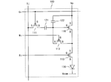
- FIG. 2 is a circuit diagram of a pixel circuit included in the display device according to the first embodiment of the present invention.
- the pixel circuit 100 shown in FIG. 2 includes a driving TFT 110, switching TFTs 111 to 113, capacitors 121 and 122, and an organic EL element 130. All of the TFTs included in the pixel circuit 100 are p-channel type.
- the pixel circuit 100 is also described in Patent Document 1 (International Publication No. 98/48403 pamphlet).
- the pixel circuit 100 is connected to the power supply wiring Vp, the common cathode Vcom, the scanning line Gi, the control wirings Wi and Ri, and the data line Sj. Among these, constant potentials VDD and VSS (where VDD> VSS) are applied to the power supply wiring Vp and the common cathode Vcom, respectively.
- the common cathode Vcom is a cathode common to all the organic EL elements 130 in the display device.
- the TFT terminals denoted as G, S, and D in FIG. 2 are referred to as a gate terminal, a source terminal, and a drain terminal, respectively.
- the lower applied voltage of two current input / output terminals is called a drain terminal, and the higher applied voltage is called a source terminal.
- the lower one of the two current input / output terminals is called a source terminal, and the higher applied voltage is called a drain terminal.
- the terminal name is changed according to the magnitude relation of the voltage, the explanation becomes complicated, so the magnitude relation of the voltage is reversed, and even when the two current input / output terminals should be called with the opposite names,
- the terminals are referred to by the names shown for convenience.
- the p-channel type is used for all TFTs, but the n-channel type may be used for the switching TFTs.
- the above description regarding the TFT terminal name and TFT type also applies to the second to fourth embodiments.
- the driving TFT 110, the switching TFT 113, and the organic EL element 130 are provided in series in this order from the power wiring Vp side between the power wiring Vp and the common cathode Vcom.
- a capacitor 121 and a switching TFT 111 are provided in series in this order from the gate terminal side.
- a switching TFT 112 is provided between the gate terminal and the drain terminal of the driving TFT 110, and a capacitor 122 is provided between the gate terminal of the driving TFT 110 and the power supply wiring Vp.
- the gate terminal of the switching TFT 111 is connected to the scanning line Gi
- the gate terminal of the switching TFT 112 is connected to the control wiring Wi
- the gate terminal of the switching TFT 113 is connected to the control wiring Ri.
- the switching TFT 111 is used as a writing switching element
- the switching TFT 112 is used as a compensation switching element
- the switching TFT 113 is used as a blocking switching element
- the capacitor 121 is used as a compensation capacitor
- the capacitor 122 is used for holding. Functions as a capacitor.
- the display device described in Patent Document 1 compensates for variations in threshold voltage of the driving TFT 110 by driving the pixel circuit 100 according to the timing chart shown in FIG.
- the pixel circuit 100 is arranged according to a timing chart (FIG. 3) different from the conventional one. To drive.
- FIG. 3 is a timing chart showing a driving method of the pixel circuit 100 in the display device according to the present embodiment.
- FIG. 3 shows changes in the potential of the data line Sj, the control wirings Wi and Ri, and the scanning line Gi, and changes in the gate terminal potential Vg of the driving TFT 110.
- the potential of the scanning line Gi and the control wiring Wi is controlled to the high level
- the potential of the control wiring Ri is controlled to the low level
- the potential of the data line Sj is controlled to the reference potential Vpc.
- the switching TFT 111 changes to a conductive state.
- the potential Vpc of the data line Sj is applied to the electrode on the switching TFT 111 side of the capacitor 121.
- the switching TFT 112 changes to a conductive state.
- the gate terminal and the drain terminal of the driving TFT 110 are short-circuited to have the same potential.
- the switching TFT 113 changes to a non-conductive state.
- a current flows from the power supply wiring Vp to the gate terminal of the driving TFT 110 via the driving TFT 110 and the switching TFT 112, and the gate terminal potential of the driving TFT 110 rises while the driving TFT 110 is in a conductive state.
- the driving TFT 110 changes to a non-conductive state when the gate-source voltage becomes the threshold voltage Vth (negative value) (that is, the gate terminal potential becomes (VDD + Vth)). Therefore, the gate terminal potential of the driving TFT 110 rises to (VDD + Vth). Up to here, it is the same as the conventional driving method.
- the potential of the data line Sj changes from the reference potential Vpc to the data potential Vdata (Vdata ⁇ Vpc except in the case of black display).
- the data potential Vdata is applied to the data line Sj while the switching TFT 112 is kept in a conductive state, and the data potential Vdata is applied to the data line Sj after the switching TFT 112 is changed to the non-conductive state. This is different from the conventional display device that gives
- FIG. 4 is a diagram illustrating a state of the pixel circuit 100 immediately after time t4.
- the driving TFT 110 changes to a conductive state as the gate-source voltage Vgs decreases (except for the case of black display).
- the switching TFT 112 is in a conductive state after time t4. For this reason, as shown in FIG. 4, immediately after time t4, the current Ia flows from the power supply wiring Vp to the gate terminal of the driving TFT 110 via the driving TFT 110 and the switching TFT 112, and the gate terminal potential of the driving TFT 110 Vg increases (in FIG. 4, the amount of increase is described as ⁇ ).
- the switching TFT 111 changes to a non-conductive state.
- the selection period of the pixel circuit 100 ends at this point.
- the potential of the data line Sj changes from the data potential Vdata to the reference potential Vpc. Since the switching TFT 111 is non-conductive after time t5, even if the potential of the data line Sj changes at time t6, the pixel circuit 100 is not affected.
- the gate-source voltage (Vth + Vdata ⁇ Vpc + ⁇ V) of the driving TFT 110 is held on the driving TFT 110 side of the capacitor 122.
- the switching TFT 113 changes to a conductive state.
- a current flows from the power supply wiring Vp to the organic EL element 130 via the driving TFT 110 and the switching TFT 113.
- the amount of current flowing through the driving TFT 110 varies depending on the gate-source voltage (Vth + Vdata ⁇ Vpc + ⁇ V) of the driving TFT 110.
- the organic EL element 130 emits light with a luminance corresponding to the current flowing through the driving TFT 110.
- the amount of current flowing through the driving TFT 110 is the same if the potential difference (Vdata ⁇ Vpc) is the same even if the threshold voltage Vth is different. For this reason, an amount of current corresponding to the data potential Vdata flows through the organic EL element 130 regardless of the value of the threshold voltage Vth, and the organic EL element 130 emits light with a luminance corresponding to the data potential Vdata.
- the display device it is possible to compensate for variations in the threshold voltage Vth of the driving TFT 110.
- ⁇ V ⁇ V
- a target value of a TFT characteristic (threshold voltage Vth, mobility ⁇ , etc.) is set in advance, and various processes are performed to bring the TFT characteristic to be close to the target value.
- the mobility ⁇ of the manufactured TFT may be larger than the target value or smaller than the target value.
- the case where the mobility ⁇ of the driving TFT 110 is equal to the target value is used as a reference.
- the current (current Ia shown in FIG. 4) flowing into the gate terminal of the driving TFT 110 during the mobility compensation period is determined by the equations (1) and (3), and increases or decreases according to the mobility ⁇ of the driving TFT 110.
- the mobility ⁇ of the driving TFT 110 is larger than the target value
- the current Ia in the mobility compensation period becomes larger than the reference.
- the change amount ⁇ V of the gate terminal potential of the driving TFT 110 during the mobility compensation period becomes larger than the reference, and the absolute value
- the mobility ⁇ of the driving TFT 110 is smaller than the target value, the current Ia in the mobility compensation period becomes smaller than the reference.
- the change amount ⁇ V of the gate terminal potential of the driving TFT 110 during the mobility compensation period becomes smaller than the reference, and the absolute value
- of the gate-source voltage of the driving TFT 110 after the mobility compensation period is small, and the reference A current that is closer to the driving TFT having the mobility of flows in the organic EL element 130 during light emission.
- of the gate-source voltage of the driving TFT 110 after the mobility compensation period is large, and the current is closer to the driving TFT having the reference mobility. Flows to the organic EL element 130 during light emission.
- an amount of current corresponding to the data potential Vdata flows through the organic EL element 130, and the organic EL element 130 emits light with a luminance corresponding to the data potential Vdata. Therefore, according to the display device according to the present embodiment, it is possible to compensate for variations in mobility of the driving TFT 110 in addition to variations in threshold voltage of the driving TFT 110.
- the timing at which the potential of the data line Sj changes from the data potential Vdata to the reference potential Vpc may be any time after the potential of the scanning line Gi has changed to a high level. That is, time t6 may be any time after time t5.
- the timing at which the potential of the control wiring Wi changes to the high level is a range after the potential of the data line Sj changes from the reference potential Vpc to the data potential Vdata and before the potential of the control wiring Ri changes to the low level. Determined within. That is, time t7 is determined within the range from time t4 to time t8. The time t7 is determined based on the mobility ⁇ of the driving TFT 110, the variation in the threshold voltage Vth, the variation in the mobility ⁇ , and the like.
- the pixel circuit 100 shown in FIG. 2 is driven according to the timing chart shown in FIG. Both of these can be compensated for and the organic EL element 130 can emit light with a desired luminance.
- FIG. 5 is a circuit diagram of a pixel circuit included in a display device according to the second embodiment of the present invention.
- a pixel circuit 200 shown in FIG. 5 includes a driving TFT 210, switching TFTs 211 to 213, a capacitor 221, and an organic EL element 230. All of the TFTs included in the pixel circuit 200 are n-channel type.
- the pixel circuit 200 is also described in another application (Japanese Patent Application No. 2008-131568) shared by the present applicant and the inventor.
- the pixel circuit 200 is connected to the power supply wiring Vp, the common cathode Vcom, the scanning line Gi, the control wiring Ri, Ui, and the data line Sj.
- constant potentials VDD and VSS are applied to the power supply wiring Vp and the common cathode Vcom, respectively.
- the common cathode Vcom is a cathode common to all the organic EL elements 230 in the display device.
- a switching TFT 213, a driving TFT 210, and an organic EL element 230 are provided in series between the power wiring Vp and the common cathode Vcom in this order from the power wiring Vp side.
- a switching TFT 211 is provided between the source terminal of the driving TFT 210 and the data line Sj
- a switching TFT 212 is provided between the gate terminal and the drain terminal of the driving TFT 210
- a capacitor 221 is provided between the control wiring Ui.
- the gate terminals of the switching TFTs 211 and 212 are both connected to the scanning line Gi, and the gate terminal of the switching TFT 213 is connected to the control wiring Ri.
- the switching TFT 211 functions as a writing switching element
- the switching TFT 212 functions as a compensation switching element
- the switching TFT 213 functions as a cutoff switching element
- the capacitor 221 functions as a compensation capacitor.
- FIG. 6 is a timing chart showing a driving method of the pixel circuit 200 in the display device according to the present embodiment.
- FIG. 6 shows changes in the potential of the scanning line Gi, the control wirings Ri and Ui, and the data line Sj, and changes in the gate terminal potential Vg of the driving TFT 210.
- Vg0 represents the gate terminal potential of the driving TFT 210 after the data potential has been written to the pixel circuit 200 last time.
- the potential of the scanning line Gi is controlled to a low level
- the potential of the control wiring Ri is controlled to a high level
- the potential of the control wiring Ui is controlled to a relatively high potential V1.
- the switching TFTs 211 and 212 are in a non-conductive state
- the switching TFT 213 is in a conductive state.
- the driving TFT 210 is in a conductive state
- a current flows from the power supply wiring Vp to the organic EL element 230 via the switching TFT 213 and the driving TFT 210, and the organic EL element 230 emits light with a predetermined luminance.
- the potential of the scanning line Gi changes to the high level, and a new data potential Vdata is applied to the data line Sj.
- the switching TFTs 211 and 212 become conductive, and the data potential Vdata is applied from the data line Sj to the source terminal of the driving TFT 210 via the switching TFT 211.
- the data potential Vdata applied at this time is determined so that the organic EL element 230 is in a non-light emitting state.
- the data potential Vdata is determined so that the difference from the potential VSS is equal to or less than the emission threshold voltage Vth_oled. . This is expressed by the following equation (6). Vth_oled ⁇ Vdata ⁇ VSS (6)
- the gate and drain of the driving TFT 210 are short-circuited, and the potential VDD is applied to the gate terminal and the drain terminal of the driving TFT 210 from the power supply wiring Vp. Therefore, the gate-source voltage Vgs of the driving TFT 210 is expressed by the following equation (7).
- Vgs VDD ⁇ Vdata (7)
- the potential of the control wiring Ui changes to a relatively low potential V2.
- the potential of the control wiring Ri changes to a low level.
- the switching TFT 213 is turned off, current flows from the gate terminal of the driving TFT 210 (and the drain terminal short-circuited thereto) to the source terminal, and the gate terminal potential of the driving TFT 210 gradually decreases.
- the driving TFT 210 becomes equal to the threshold voltage Vth of the driving TFT 210 (that is, when the gate terminal potential becomes (Vdata + Vth)
- the driving TFT 210 becomes non-conductive and is driven. After that, the gate terminal potential of the TFT 210 does not decrease.
- the driving TFT 210 is in a state where the threshold voltage Vth is applied between the gate and the source regardless of the threshold voltage Vth.
- the lifetime of the organic EL element becomes shorter as a larger amount of current flows. Therefore, in order to prevent a current from flowing through the organic EL element 230, it is preferable to use the data potential Vdata that satisfies Expression (6).
- the data potential Vdata is used, either the anode and the cathode of the organic EL element 230 are at the same potential, or a reverse bias voltage is applied to the organic EL element 230. Thereby, it is possible to prevent a current from flowing into the organic EL element 230 after the time t3 and extend the life of the organic EL element 230.
- the potential of the control wiring Ui changes from V2 to V1.
- the control wiring Ui and the gate terminal of the driving TFT 210 are connected via a capacitor 221.
- the gate terminal potential of the driving TFT 210 changes by the same amount (V1-V2), as shown in the following equation (8).
- Vg Vdata + Vth + V1-V2 (8)
- FIG. 7 is a diagram illustrating a state of the pixel circuit 200 immediately after time t4.
- the driving TFT 210 changes to a conductive state as the gate-source voltage Vgs increases (except for the case of black display).
- the switching TFT 212 is in a conductive state after time t4. For this reason, as shown in FIG. 7, immediately after time t4, data is transferred from the gate terminal of the driving TFT 210 (and the drain terminal short-circuited thereto) via the switching TFT 212, the driving TFT 210, and the switching TFT 211.
- the current Ib flows out to the line Sj, and the gate terminal potential Vg of the driving TFT 210 decreases (the amount of decrease is described as ⁇ in FIG. 7).
- the switching TFTs 211 and 212 change to a non-conduction state. If the change amount of the gate terminal potential of the driving TFT 210 from time t4 to time t5 (hereinafter referred to as mobility compensation period) is ⁇ V (where ⁇ V> 0), the gate terminal of the driving TFT 210 at time t5
- the potential Vg is as shown in the following formula (9).
- Vg Vdata + Vth + V1-V2- ⁇ V (9)
- the potential difference between the electrodes of the capacitor 221 is (Vdata + Vth ⁇ V2 ⁇ V). After the time t5, the potential difference is held in the capacitor 221. Note that the time t5 is determined based on the mobility ⁇ of the driving TFT 210, the variation in the threshold voltage Vth, the variation in the mobility ⁇ , and the like.
- the switching TFT 213 changes to a conductive state, and the potential VDD is applied to the drain terminal of the driving TFT 210 from the power supply wiring Vp.
- the gate terminal potential of the driving TFT 210 is kept at (Vdata + Vth + V1-V2- ⁇ V) after time t6. Therefore, after time t6, the potential (Vdata + V1-V2-) is obtained by subtracting the threshold voltage Vth of the driving TFT 210 from the gate terminal potential from the power supply wiring Vp via the switching TFT 213 and the organic EL element 230 to the organic EL element 230.
- a current corresponding to ⁇ V) flows, and the organic EL element 230 emits light with a luminance corresponding to the current.
- the data potential Vdata applied to the data line Sj during the period when the potential of the scanning line Gi is at a high level should be originally applied in order to cause the organic EL element 230 to emit light with a desired luminance.
- the potential is set by subtracting the amplitude (V1-V2) of the potential of the control wiring Ui from the data potential Vdata ′. This can be expressed by the following equation (10).
- Vdata Vdata ′ ⁇ (V1 ⁇ V2) (10)
- the mobility ⁇ of the driving TFT 210 when the mobility ⁇ of the driving TFT 210 is smaller than the target value, the current Ib in the mobility compensation period becomes smaller than the reference. Therefore, the amount of change ⁇ V in the gate terminal potential of the driving TFT 210 during the mobility compensation period becomes smaller than the reference, and the absolute value
- the absolute value of the gate-source voltage of the driving TFT 210 after the mobility compensation period is the same as in the first embodiment.
- becomes smaller, and a current closer to the driving TFT having the reference mobility flows to the organic EL element 230 during light emission.
- the mobility ⁇ of the driving TFT 210 is small, the absolute value
- the organic EL element 230 does not emit light only by writing the potential of the data line Sj to the pixel circuit 200.
- the gate driver circuit 12 changes the potential of the control wiring Ui in two steps (V1 and V2).
- the inverter circuit shown in FIG. 8 is provided as a buffer circuit at the final stage of the gate driver circuit 12.
- the inverter circuit shown in FIG. 8 changes the potential of the control wiring Ui in two steps according to the input signal IN.
- the display device includes a gate driver circuit 12 that changes the potential of the control wiring Ui in two stages. Such a gate driver circuit can be easily configured.
- the timing at which the potential of the control wiring Ui changes from V1 to V2 may be before the potential of the scanning line Gi changes to a high level. That is, time t2 may be before time t1.
- this method even when the number of scanning lines Gi is large and the time during which the potential of the scanning line Gi is at a high level is short, variations in threshold voltage and mobility in the driving TFT 210 can be compensated.
- a forward bias voltage is applied to the organic EL element 230, the organic EL element 230 may emit light unnecessarily, and the contrast of the screen may be lowered. Therefore, as shown in FIG. 6, it is more preferable that the potential of the control wiring Ui changes from V1 to V2 after the potential of the scanning line Gi changes to the high level.
- the gate terminals of the switching TFTs 211 and 212 are connected to the same scanning line Gi.
- the switching TFTs 211 and 212 may be connected to different control wirings that change at almost the same timing. Good.
- the pixel circuit 200 shown in FIG. 5 is driven according to the timing chart shown in FIG. Both can be compensated for, and the organic EL element 230 can emit light with a desired luminance.
- the display device according to the third embodiment of the present invention includes the pixel circuit 200 shown in FIG.
- the display device according to the present embodiment drives the pixel circuit 200 according to a timing chart (FIG. 9) different from that of the second embodiment.
- FIG. 9 is a timing chart showing a driving method of the pixel circuit 200 in the display device according to the present embodiment.
- the potential of the data line Sj becomes the reference potential Vpc higher than the data potential Vdata from time t4 to time t5 (mobility compensation period).
- the timing chart shown in FIG. 9 is the same as the timing chart shown in FIG.
- the potential of the data line Sj is driven higher than the data potential Vdata after the potential of the control wiring Ui is changed from V2 to V1 (potential at which the driving TFT 210 is turned on). It changes to a potential close to the gate terminal potential of the TFT 210 for use.
- the reference potential Vpc is determined so as to be lower than the gate terminal potential of the driving TFT 210 when the data potential Vdata is the minimum in order to prevent gradation inversion. That is, when the data potential Vdata when displaying the minimum gradation is Vm, the reference potential Vpc is determined so as to satisfy the following equation (11). Vpc ⁇ Vm + Vth + V1-V2 (11)
- the pixel circuit 200 by driving the pixel circuit 200 according to the timing chart shown in FIG. 9, similarly to the second embodiment, the pixel circuit 200 is not affected by variations in the threshold voltage of the driving TFT 210.
- a current that is not affected by variations in mobility of the driving TFT 210 can be passed through the organic EL element 230 to compensate for both variations in threshold voltage and mobility in the organic EL element 230.
- FIG. 10 is a diagram illustrating a state of the pixel circuit 200 immediately after time t4 in the display device according to the present embodiment. Also in the display device according to the present embodiment, as in the second embodiment, after time t4, the current Ic flows from the gate terminal of the driving TFT 210 to the data line Sj, and the gate terminal potential Vg of the driving TFT 210 drops ( In FIG. 10, the descending amount is indicated as ⁇ ).
- some TFTs have high mobility.
- the mobility of amorphous silicon TFTs is less than 10 cm 2 / Vs, while the mobility of low-temperature polysilicon TFTs or CG silicon TFTs exceeds 100 cm 2 / Vs. Therefore, when the display device according to the second embodiment is configured using TFTs having high mobility, the amount of change ⁇ V in the gate terminal potential of the driving TFT 210 during the mobility compensation period increases, and the threshold value of the driving TFT 210 is increased. Voltage variations may not be compensated correctly.
- the reference potential Vpc applied to the data line Sj after time t4 is closer to the gate terminal potential of the driving TFT 210 than the data potential Vdata. Therefore, the current Ic flowing from the gate terminal of the driving TFT 210 to the data line Sj after time t4 is smaller than that in the second embodiment (Ic ⁇ Ib), and the amount of change in the gate terminal potential Vg of the driving TFT 210 is also the first. It is smaller than the second embodiment ( ⁇ ⁇ ). As a result, the amount of change in the gate terminal potential of the driving TFT 210 during the mobility compensation period is smaller than that in the second embodiment.
- the display device of this embodiment even when the mobility of the driving TFT 210 is large, the influence of the mobility of the driving TFT 210 on the gate terminal potential of the driving TFT 210 is reduced, and the driving TFT 210 Both variation in threshold voltage and variation in mobility can be compensated.
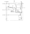
- FIG. 11 is a circuit diagram of a pixel circuit included in a display device according to the fourth embodiment of the present invention.
- a pixel circuit 300 shown in FIG. 11 includes a driving TFT 310, switching TFTs 311 to 315, a capacitor 321, and an organic EL element 330. All of the TFTs included in the pixel circuit 300 are p-channel type.
- the pixel circuit 300 is a modification of the pixel circuit (FIG. 14) described in Patent Document 2 (Japanese Patent Laid-Open No. 2007-133369) so that the gate terminals of all the switching TFTs are connected to different signal lines. It is a thing.
- the pixel circuit 300 is connected to power supply wirings Vp and Vint, a common cathode Vcom, scanning lines G1i, G2i, and G3i, control wirings E1i and E2i, and a data line Sj.
- constant potentials VDD and VSS are applied to the power supply wiring Vp and the common cathode Vcom, respectively, and a constant potential Vpc is applied to the power supply wiring Vint.
- the common cathode Vcom is a cathode common to all the organic EL elements 330 in the display device.
- a driving TFT 310, a switching TFT 313, and an organic EL element 330 are provided in series between the power wiring Vp and the common cathode Vcom in this order from the power wiring Vp side.
- a capacitor 321 and a switching TFT 311 are provided in series in this order from the gate terminal side.
- a switching TFT 312 is provided between the gate terminal and the drain terminal of the driving TFT 310.
- a connection point between the switching TFT 311 and the capacitor 321 is referred to as a connection point A.
- a switching TFT 314 is provided between the connection point A and the power supply wiring Vint
- a switching TFT 315 is provided between the drain terminal of the driving TFT 310 and the power supply wiring Vint.
- the gate terminal of the switching TFT 311 is connected to the scanning line G1i
- the gate terminal of the switching TFT 312 is connected to the scanning line G3i
- the gate terminal of the switching TFT 313 is connected to the control wiring E2i
- the gate terminal of the switching TFT 314 is controlled.
- Connected to the wiring E1i the gate terminal of the switching TFT 315 is connected to the scanning line G2i.
- the scanning lines G1i, G2i, and G3i correspond to the scanning lines Gi in FIG.
- the switching TFT 311 is used as a writing switching element
- the switching TFT 312 is used as a compensation switching element
- the switching TFT 313 is used as a blocking switching element
- the switching TFT 314 is used as a first initialization switching element.
- the switching TFT 315 functions as a second initialization switching element
- the capacitor 321 functions as a compensation capacitor.
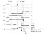
- FIG. 12 is a timing chart showing a driving method of the pixel circuit 300 in the display device according to the present embodiment.
- FIG. 12 shows changes in the potentials of the scanning lines G1i, G2i, G3i, the control wirings E1i, E2i, and the data line Sj, and changes in the gate terminal potential Vg of the driving TFT 310.
- the potentials of the scanning lines G1i, G2i, G3i are controlled to a high level, and the potentials of the control wirings E1i, E2i are controlled to a low level.
- the switching TFTs 313 and 314 change to a non-conduction state.
- the switching TFTs 311, 312, and 315 change to a conductive state.
- the gate terminal and the drain terminal of the driving TFT 310 are short-circuited to have the same potential, and the gate terminal potential Vg of the driving TFT 310 becomes equal to the potential Vpc of the power supply wiring Vint.
- the potential Vdata of the data line Sj is applied to the connection point A.
- the switching TFT 315 changes to a non-conduction state.
- a current flows from the power supply wiring Vp to the gate terminal of the driving TFT 310 via the driving TFT 310 and the switching TFT 312, and the gate terminal potential Vg of the driving TFT 310 increases while the driving TFT 310 is in a conductive state.
- the driving TFT 310 changes to a non-conductive state when the gate-source voltage becomes the threshold voltage Vth (negative value)
- the gate terminal potential Vg of the driving TFT 310 rises to (VDD + Vth).
- the switching TFT 311 changes to a non-conduction state
- the switching TFT 314 changes to a conduction state.
- the potential at the connection point A changes from Vdata to Vpc
- the gate terminal potential Vg of the driving TFT 310 changes by the same amount as the potential at the connection point A.
- the gate terminal potential Vg and the gate-source voltage Vgs of the driving TFT 310 at time t4 are as shown in the following equations (12) and (13), respectively.
- Vg VDD + Vth + (Vpc ⁇ Vdata) (12)
- Vgs Vth + (Vpc ⁇ Vdata) (13)
- the gate-source voltage (Vth + Vpc ⁇ Vdata) of the driving TFT 310 is temporarily held on the driving TFT 310 side of the capacitor 321.
- a current flows from the power supply wiring Vp to the gate terminal of the driving TFT 310 via the driving TFT 310 and the switching TFT 312 and the gate terminal potential Vg of the driving TFT 310 rises.
- the switching TFT 313 changes to a conductive state.
- a current flows from the power supply wiring Vp to the organic EL element 330 via the driving TFT 310 and the switching TFT 313.
- the amount of current flowing through the driving TFT 310 varies according to the gate-source voltage (Vth + Vpc ⁇ Vdata + ⁇ V) of the driving TFT 310.
- the organic EL element 330 emits light with a luminance corresponding to the current flowing through the driving TFT 310.
- the current flowing into the gate terminal of the driving TFT 310 during the mobility compensation period is determined by equations (1) and (13), and increases or decreases according to the mobility ⁇ of the driving TFT 310.
- the mobility ⁇ of the driving TFT 310 is larger than the target value, the current in the mobility compensation period becomes larger than the reference.
- the change amount ⁇ V of the gate terminal potential of the driving TFT 310 during the mobility compensation period becomes larger than the reference, and the absolute value
- the mobility ⁇ of the driving TFT 310 is smaller than the target value, the current in the mobility compensation period becomes smaller than the reference. For this reason, the change amount ⁇ V of the gate terminal potential of the driving TFT 310 during the mobility compensation period becomes smaller than the reference, and the absolute value
- an amount of current corresponding to the data potential Vdata flows through the organic EL element 330, and the organic EL element 330 emits light with a luminance corresponding to the data potential Vdata. Therefore, according to the display device according to this embodiment, it is possible to compensate for variations in mobility of the driving TFT 310 in addition to variations in threshold voltage of the driving TFT 310.
- the pixel circuit 300 shown in FIG. 11 is driven according to the timing chart shown in FIG. Both of these can be compensated for and the organic EL element 330 can emit light with a desired luminance.
- the pixel circuit includes an organic EL element as an electro-optical element.
- the pixel circuit is an electro-optical element other than an organic EL element such as a semiconductor LED (Light Emitting Diode) or a light emitting unit of an FED.
- the current drive type electro-optical element may be included.
- the pixel circuit is a MOS transistor (herein referred to as a MOS transistor including a silicon gate MOS structure) formed on an insulating substrate such as a glass substrate as a driving element for the electro-optical element. TFT was included.
- the pixel circuit is not limited to this, and the pixel circuit has an arbitrary control voltage (threshold voltage) that changes the output current according to the control voltage applied to the current control terminal as the driving element of the electro-optical element and makes the output current zero.
- a voltage-controlled element may be included.
- a general insulated gate field effect transistor including, for example, a MOS transistor formed on a semiconductor substrate can be used as the drive element of the electro-optic element.
- the display device of the present invention has an effect of being able to compensate for both of the threshold voltage variation and the mobility variation of the drive element, various display devices including current-driven display elements such as an organic EL display and FED. Can be used.
Abstract
Description
Ids=(1/2)・(W/L)・μ・Cox(Vgs-Vth)2 …(1)
ただし、式(1)において、Wは駆動用TFT110のチャネル幅、Lは駆動用TFT110のチャネル長、μは駆動用TFT110の移動度、Coxは駆動用TFT110のゲート酸化膜容量、Vthは駆動用TFT110の閾値電圧を表す。
複数の走査線と複数のデータ線の各交差点に対応して配置された複数の画素回路と、
前記走査線を用いて書き込み対象の画素回路を選択し、前記データ線に対して表示データに応じたデータ電位を与える駆動回路とを備え、
前記画素回路は、
第1の電源配線と第2の電源配線との間に設けられた電気光学素子と、
前記第1の電源配線と前記第2の電源配線との間に前記電気光学素子と直列に設けられた駆動素子と、
前記駆動素子の制御端子に第1の電極が接続された補償用コンデンサと、
前記駆動素子の制御端子と一方の電流入出力端子との間に設けられた補償用スイッチング素子とを含み、
前記駆動回路は、書き込み対象の画素回路について、前記補償用スイッチング素子を導通状態に制御して前記駆動素子の制御端子に閾値電圧に応じた電位を与え、その後に、前記補償用スイッチング素子を導通状態に保ったままで前記補償用コンデンサの第2の電極に与える電位を切り替えて、前記駆動素子の制御端子に前記表示データと前記閾値電圧に応じた書き込み電位を与えることを特徴とする。
前記画素回路は、
前記補償用コンデンサの第2の電極と前記データ線との間に設けられた書き込み用スイッチング素子と、
前記駆動素子と前記電気光学素子との間に設けられた遮断用スイッチング素子と、
前記駆動素子の制御端子と他方の電流入出力端子との間に設けられた保持用コンデンサとをさらに含む。
前記駆動回路は、書き込み対象の画素回路について、前記データ線に所定の基準電位を与えながら、前記書き込み用スイッチング素子と前記補償用スイッチング素子を導通状態に、前記遮断用スイッチング素子を非導通状態に制御し、その後に、各スイッチング素子の状態を保ったままで、前記データ線に与える電位を前記データ電位に切り替えることを特徴とする。
前記画素回路は、
前記駆動素子の一方の電流入出力端子と前記第1の電源配線との間に設けられた遮断用スイッチング素子と、
前記駆動素子の他方の電流入出力端子と前記データ線との間に設けられた書き込み用スイッチング素子とをさらに含み、
前記補償用コンデンサの第2の電極は、前記駆動回路が電位を与える制御配線に接続されていることを特徴とする。
前記駆動回路は、書き込み対象の画素回路について、前記データ線に前記データ電位を与えながら、前記書き込み用スイッチング素子と前記補償用スイッチング素子を導通状態に、前記遮断用スイッチング素子を非導通状態に制御し、その後に、各スイッチング素子の状態を保ったままで、前記駆動素子の制御端子に前記書き込み電位が与えられるように前記制御配線に与える電位を切り替えることを特徴とする。
前記駆動回路は、前記駆動素子の制御端子に前記書き込み電位が与えられるように前記制御配線に与える電位を切り替えた後に、前記データ線に与える電位を前記データ電位よりも前記駆動素子の制御端子の電位に近い基準電位に切り替えることを特徴とする。
前記駆動回路は、書き込み対象の画素回路について、前記書き込み用スイッチング素子を導通状態に制御している間、前記データ線に対して、前記表示データと前記制御配線に与える電位の変化量とによって定まる電位を与えることを特徴とする。
前記駆動回路は、書き込み対象の画素回路について、前記書き込み用スイッチング素子を導通状態に制御している間、前記データ線に対して、前記電気光学素子への印加電圧が発光閾値電圧以下となる電位を与えることを特徴とする。
前記画素回路は、
前記補償用コンデンサの第2の電極と前記データ線との間に設けられた書き込み用スイッチング素子と、
前記駆動素子と前記電気光学素子との間に設けられた遮断用スイッチング素子と、
前記補償用コンデンサの第2の電極と第3の電源配線との間に設けられた第1の初期化用スイッチング素子と、
前記駆動素子の一方の電流入出力端子と前記第3の電源配線との間に設けられた第2の初期化用スイッチング素子とをさらに含む。
前記駆動回路は、書き込み対象の画素回路について、前記データ線に対して前記データ電位を与えながら、前記書き込み用スイッチング素子と前記補償用スイッチング素子と前記第2の初期化用スイッチング素子を導通状態に、前記遮断用スイッチング素子と前記第1の初期化用スイッチング素子を非導通状態に制御し、その後に、前記補償用スイッチング素子を導通状態に保ったままで、前記書き込み用スイッチング素子を非導通状態に、前記第1の初期化用スイッチング素子を導通状態に制御することを特徴とする。
前記画素回路が、第1の電源配線と第2の電源配線との間に設けられた電気光学素子と、前記第1の電源配線と前記第2の電源配線との間に前記電気光学素子と直列に設けられた駆動素子と、前記駆動素子の制御端子に第1の電極が接続された補償用コンデンサと、前記駆動素子の制御端子と一方の電流入出力端子との間に設けられた補償用スイッチング素子とを含む場合に、
前記走査線を用いて書き込み対象の画素回路を選択する選択ステップと、
書き込み対象の画素回路について、前記補償用スイッチング素子を導通状態に制御して前記駆動素子の制御端子に閾値電圧に応じた電位を与える閾値状態設定ステップと、
前記閾値状態設定ステップの後に、書き込み対象の画素回路について、前記補償用スイッチング素子を導通状態に保ったままで前記補償用コンデンサの第2の電極に与える電位を切り替えて、前記駆動素子の制御端子に表示データと前記閾値電圧に応じた書き込み電位を与える導通状態設定ステップとを備える。
前記画素回路が、前記補償用コンデンサの第2の電極と前記データ線との間に設けられた書き込み用スイッチング素子と、前記駆動素子と前記電気光学素子との間に設けられた遮断用スイッチング素子と、前記駆動素子の制御端子と他方の電流入出力端子との間に設けられた保持用コンデンサとをさらに含む場合に、
前記閾値状態設定ステップは、書き込み対象の画素回路について、前記データ線に所定の基準電位を与えながら、前記書き込み用スイッチング素子と前記補償用スイッチング素子を導通状態に、前記遮断用スイッチング素子を非導通状態に制御し、
前記導通状態設定ステップは、各スイッチング素子の状態を保ったままで、前記データ線に与える電位を前記表示データに応じたデータ電位に切り替えることを特徴とする。
前記画素回路が、前記駆動素子の一方の電流入出力端子と前記第1の電源配線との間に設けられた遮断用スイッチング素子と、前記駆動素子の他方の電流入出力端子と前記データ線との間に設けられた書き込み用スイッチング素子とをさらに含み、前記補償用コンデンサの第2の電極が制御配線に接続されている場合に、
前記閾値状態設定ステップは、書き込み対象の画素回路について、前記データ線に対して前記表示データに応じたデータ電位を与えながら、前記書き込み用スイッチング素子と前記補償用スイッチング素子を導通状態に、前記遮断用スイッチング素子を非導通状態に制御し、
前記導通状態設定ステップは、各スイッチング素子の状態を保ったままで、前記駆動素子の制御端子に前記書き込み電位が与えられるように前記制御配線に与える電位を切り替えることを特徴とする。
前記画素回路が、前記補償用コンデンサの第2の電極と前記データ線との間に設けられた書き込み用スイッチング素子と、前記駆動素子と前記電気光学素子との間に設けられた遮断用スイッチング素子と、前記補償用コンデンサの第2の電極と第3の電源配線との間に設けられた第1の初期化用スイッチング素子と、前記駆動素子の一方の電流入出力端子と前記第3の電源配線との間に設けられた第2の初期化用スイッチング素子とをさらに含む場合に、
前記閾値状態設定ステップは、書き込み対象の画素回路について、前記データ線に対して前記表示データに応じたデータ電位を与えながら、前記書き込み用スイッチング素子と前記補償用スイッチング素子と前記第2の初期化用スイッチング素子を導通状態に、前記遮断用スイッチング素子と前記第1の初期化用スイッチング素子を非導通状態に制御し、
前記導通状態設定ステップは、前記補償用スイッチング素子を導通状態に保ったままで、前記書き込み用スイッチング素子を非導通状態に、前記第1の初期化用スイッチング素子を導通状態に制御することを特徴とする。
図2は、本発明の第1の実施形態に係る表示装置に含まれる画素回路の回路図である。図2に示す画素回路100は、駆動用TFT110、スイッチ用TFT111~113、コンデンサ121、122、および、有機EL素子130を備えている。画素回路100に含まれるTFTは、いずれもpチャネル型である。画素回路100は、特許文献1(国際公開第98/48403号パンフレット)にも記載されている。
Vg =VDD+Vth+(Vdata-Vpc) …(2)
Vgs=Vth+(Vdata-Vpc) …(3)
Vg =VDD+Vth+(Vdata-Vpc)+ΔV …(4)
Vgs=Vth+(Vdata-Vpc)+ΔV …(5)
図5は、本発明の第2の実施形態に係る表示装置に含まれる画素回路の回路図である。図5に示す画素回路200は、駆動用TFT210、スイッチ用TFT211~213、コンデンサ221、および、有機EL素子230を備えている。画素回路200に含まれるTFTは、いずれもnチャネル型である。画素回路200は、本出願と出願人および発明者が共通する別の出願(日本国特願2008-131568号)にも記載されている。
Vth_oled≧Vdata-VSS …(6)
Vgs=VDD-Vdata …(7)
Vg=Vdata+Vth+V1-V2 …(8)
Vg=Vdata+Vth+V1-V2-ΔV …(9)
Vdata=Vdata’-(V1-V2) …(10)
本発明の第3の実施形態に係る表示装置は、第2の実施形態に係る表示装置と同じく、図5に示す画素回路200を備えている。本実施形態に係る表示装置は、画素回路200を第2の実施形態とは異なるタイミングチャート(図9)に従って駆動する。
Vpc<Vm+Vth+V1-V2 …(11)
図11は、本発明の第4の実施形態に係る表示装置に含まれる画素回路の回路図である。図11に示す画素回路300は、駆動用TFT310、スイッチ用TFT311~315、コンデンサ321、および、有機EL素子330を備えている。画素回路300に含まれるTFTは、いずれもpチャネル型である。画素回路300は、特許文献2(日本国特開2007-133369号公報)に記載された画素回路(図14)を、すべてのスイッチ用TFTのゲート端子を互いに異なる信号線に接続するように変形したものである。
Vg =VDD+Vth+(Vpc-Vdata) …(12)
Vgs=Vth+(Vpc-Vdata) …(13)
Vg =VDD+Vth+(Vpc-Vdata)+ΔV …(14)
Vgs=Vth+(Vpc-Vdata)+ΔV …(15)
11…表示制御回路
12…ゲートドライバ回路
13…ソースドライバ回路
21…シフトレジスタ
22…レジスタ
23…ラッチ回路
24…D/A変換器
100、200、300、Aij…画素回路
110、210、310…駆動用TFT
111~113、211~213、311~315…スイッチ用TFT
121、122、221、321…コンデンサ
130、230、330…有機EL素子
Gi、G1i、G2i、G3i…走査線
Ri、Ui、Wi、E1i、E2i…制御配線
Sj…データ線
Vp…電源配線
Vcom…共通陰極
Claims (14)
- 電流駆動型の表示装置であって、
複数の走査線と複数のデータ線の各交差点に対応して配置された複数の画素回路と、
前記走査線を用いて書き込み対象の画素回路を選択し、前記データ線に対して表示データに応じたデータ電位を与える駆動回路とを備え、
前記画素回路は、
第1の電源配線と第2の電源配線との間に設けられた電気光学素子と、
前記第1の電源配線と前記第2の電源配線との間に前記電気光学素子と直列に設けられた駆動素子と、
前記駆動素子の制御端子に第1の電極が接続された補償用コンデンサと、
前記駆動素子の制御端子と一方の電流入出力端子との間に設けられた補償用スイッチング素子とを含み、
前記駆動回路は、書き込み対象の画素回路について、前記補償用スイッチング素子を導通状態に制御して前記駆動素子の制御端子に閾値電圧に応じた電位を与え、その後に、前記補償用スイッチング素子を導通状態に保ったままで前記補償用コンデンサの第2の電極に与える電位を切り替えて、前記駆動素子の制御端子に前記表示データと前記閾値電圧に応じた書き込み電位を与えることを特徴とする、表示装置。 - 前記画素回路は、
前記補償用コンデンサの第2の電極と前記データ線との間に設けられた書き込み用スイッチング素子と、
前記駆動素子と前記電気光学素子との間に設けられた遮断用スイッチング素子と、
前記駆動素子の制御端子と他方の電流入出力端子との間に設けられた保持用コンデンサとをさらに含む、請求項1に記載の表示装置。 - 前記駆動回路は、書き込み対象の画素回路について、前記データ線に所定の基準電位を与えながら、前記書き込み用スイッチング素子と前記補償用スイッチング素子を導通状態に、前記遮断用スイッチング素子を非導通状態に制御し、その後に、各スイッチング素子の状態を保ったままで、前記データ線に与える電位を前記データ電位に切り替えることを特徴とする、請求項2に記載の表示装置。
- 前記画素回路は、
前記駆動素子の一方の電流入出力端子と前記第1の電源配線との間に設けられた遮断用スイッチング素子と、
前記駆動素子の他方の電流入出力端子と前記データ線との間に設けられた書き込み用スイッチング素子とをさらに含み、
前記補償用コンデンサの第2の電極は、前記駆動回路が電位を与える制御配線に接続されていることを特徴とする、請求項1に記載の表示装置。 - 前記駆動回路は、書き込み対象の画素回路について、前記データ線に前記データ電位を与えながら、前記書き込み用スイッチング素子と前記補償用スイッチング素子を導通状態に、前記遮断用スイッチング素子を非導通状態に制御し、その後に、各スイッチング素子の状態を保ったままで、前記駆動素子の制御端子に前記書き込み電位が与えられるように前記制御配線に与える電位を切り替えることを特徴とする、請求項4に記載の表示装置。
- 前記駆動回路は、前記駆動素子の制御端子に前記書き込み電位が与えられるように前記制御配線に与える電位を切り替えた後に、前記データ線に与える電位を前記データ電位よりも前記駆動素子の制御端子の電位に近い基準電位に切り替えることを特徴とする、請求項5に記載の表示装置。
- 前記駆動回路は、書き込み対象の画素回路について、前記書き込み用スイッチング素子を導通状態に制御している間、前記データ線に対して、前記表示データと前記制御配線に与える電位の変化量とによって定まる電位を与えることを特徴とする、請求項5に記載の表示装置。
- 前記駆動回路は、書き込み対象の画素回路について、前記書き込み用スイッチング素子を導通状態に制御している間、前記データ線に対して、前記電気光学素子への印加電圧が発光閾値電圧以下となる電位を与えることを特徴とする、請求項5に記載の表示装置。
- 前記画素回路は、
前記補償用コンデンサの第2の電極と前記データ線との間に設けられた書き込み用スイッチング素子と、
前記駆動素子と前記電気光学素子との間に設けられた遮断用スイッチング素子と、
前記補償用コンデンサの第2の電極と第3の電源配線との間に設けられた第1の初期化用スイッチング素子と、
前記駆動素子の一方の電流入出力端子と前記第3の電源配線との間に設けられた第2の初期化用スイッチング素子とをさらに含む、請求項1に記載の表示装置。 - 前記駆動回路は、書き込み対象の画素回路について、前記データ線に対して前記データ電位を与えながら、前記書き込み用スイッチング素子と前記補償用スイッチング素子と前記第2の初期化用スイッチング素子を導通状態に、前記遮断用スイッチング素子と前記第1の初期化用スイッチング素子を非導通状態に制御し、その後に、前記補償用スイッチング素子を導通状態に保ったままで、前記書き込み用スイッチング素子を非導通状態に、前記第1の初期化用スイッチング素子を導通状態に制御することを特徴とする、請求項9に記載の表示装置。
- 複数の走査線と複数のデータ線の各交差点に対応して配置された複数の画素回路を備えた電流駆動型の表示装置の駆動方法であって、
前記画素回路が、第1の電源配線と第2の電源配線との間に設けられた電気光学素子と、前記第1の電源配線と前記第2の電源配線との間に前記電気光学素子と直列に設けられた駆動素子と、前記駆動素子の制御端子に第1の電極が接続された補償用コンデンサと、前記駆動素子の制御端子と一方の電流入出力端子との間に設けられた補償用スイッチング素子とを含む場合に、
前記走査線を用いて書き込み対象の画素回路を選択する選択ステップと、
書き込み対象の画素回路について、前記補償用スイッチング素子を導通状態に制御して前記駆動素子の制御端子に閾値電圧に応じた電位を与える閾値状態設定ステップと、
前記閾値状態設定ステップの後に、書き込み対象の画素回路について、前記補償用スイッチング素子を導通状態に保ったままで前記補償用コンデンサの第2の電極に与える電位を切り替えて、前記駆動素子の制御端子に表示データと前記閾値電圧に応じた書き込み電位を与える導通状態設定ステップとを備えた、表示装置の駆動方法。 - 前記画素回路が、前記補償用コンデンサの第2の電極と前記データ線との間に設けられた書き込み用スイッチング素子と、前記駆動素子と前記電気光学素子との間に設けられた遮断用スイッチング素子と、前記駆動素子の制御端子と他方の電流入出力端子との間に設けられた保持用コンデンサとをさらに含む場合に、
前記閾値状態設定ステップは、書き込み対象の画素回路について、前記データ線に所定の基準電位を与えながら、前記書き込み用スイッチング素子と前記補償用スイッチング素子を導通状態に、前記遮断用スイッチング素子を非導通状態に制御し、
前記導通状態設定ステップは、各スイッチング素子の状態を保ったままで、前記データ線に与える電位を前記表示データに応じたデータ電位に切り替えることを特徴とする、請求項11に記載の駆動方法。 - 前記画素回路が、前記駆動素子の一方の電流入出力端子と前記第1の電源配線との間に設けられた遮断用スイッチング素子と、前記駆動素子の他方の電流入出力端子と前記データ線との間に設けられた書き込み用スイッチング素子とをさらに含み、前記補償用コンデンサの第2の電極が制御配線に接続されている場合に、
前記閾値状態設定ステップは、書き込み対象の画素回路について、前記データ線に対して前記表示データに応じたデータ電位を与えながら、前記書き込み用スイッチング素子と前記補償用スイッチング素子を導通状態に、前記遮断用スイッチング素子を非導通状態に制御し、
前記導通状態設定ステップは、各スイッチング素子の状態を保ったままで、前記駆動素子の制御端子に前記書き込み電位が与えられるように前記制御配線に与える電位を切り替えることを特徴とする、請求項11に記載の駆動方法。 - 前記画素回路が、前記補償用コンデンサの第2の電極と前記データ線との間に設けられた書き込み用スイッチング素子と、前記駆動素子と前記電気光学素子との間に設けられた遮断用スイッチング素子と、前記補償用コンデンサの第2の電極と第3の電源配線との間に設けられた第1の初期化用スイッチング素子と、前記駆動素子の一方の電流入出力端子と前記第3の電源配線との間に設けられた第2の初期化用スイッチング素子とをさらに含む場合に、
前記閾値状態設定ステップは、書き込み対象の画素回路について、前記データ線に対して前記表示データに応じたデータ電位を与えながら、前記書き込み用スイッチング素子と前記補償用スイッチング素子と前記第2の初期化用スイッチング素子を導通状態に、前記遮断用スイッチング素子と前記第1の初期化用スイッチング素子を非導通状態に制御し、
前記導通状態設定ステップは、前記補償用スイッチング素子を導通状態に保ったままで、前記書き込み用スイッチング素子を非導通状態に、前記第1の初期化用スイッチング素子を導通状態に制御することを特徴とする、請求項11に記載の駆動方法。
Priority Applications (4)
| Application Number | Priority Date | Filing Date | Title |
|---|---|---|---|
| JP2010523796A JP5199367B2 (ja) | 2008-08-07 | 2009-06-01 | 表示装置およびその駆動方法 |
| US12/737,294 US8674914B2 (en) | 2008-08-07 | 2009-06-01 | Display device and method of driving the same |
| CN200980126608.6A CN102089798B (zh) | 2008-08-07 | 2009-06-01 | 显示装置及其驱动方法 |
| EP09804803.6A EP2309478B1 (en) | 2008-08-07 | 2009-06-01 | Display apparatus and method of driving the same |
Applications Claiming Priority (2)
| Application Number | Priority Date | Filing Date | Title |
|---|---|---|---|
| JP2008203765 | 2008-08-07 | ||
| JP2008-203765 | 2008-08-07 |
Publications (1)
| Publication Number | Publication Date |
|---|---|
| WO2010016316A1 true WO2010016316A1 (ja) | 2010-02-11 |
Family
ID=41663541
Family Applications (1)
| Application Number | Title | Priority Date | Filing Date |
|---|---|---|---|
| PCT/JP2009/059946 WO2010016316A1 (ja) | 2008-08-07 | 2009-06-01 | 表示装置およびその駆動方法 |
Country Status (6)
| Country | Link |
|---|---|
| US (1) | US8674914B2 (ja) |
| EP (1) | EP2309478B1 (ja) |
| JP (3) | JP5199367B2 (ja) |
| CN (2) | CN102089798B (ja) |
| RU (1) | RU2457551C1 (ja) |
| WO (1) | WO2010016316A1 (ja) |
Cited By (8)
| Publication number | Priority date | Publication date | Assignee | Title |
|---|---|---|---|---|
| JP2012003205A (ja) * | 2010-06-21 | 2012-01-05 | Canon Inc | 表示装置およびその駆動方法 |
| JP2012033447A (ja) * | 2010-08-03 | 2012-02-16 | Nec Lighting Ltd | 照明装置およびその制御方法 |
| US20120127150A1 (en) * | 2010-11-18 | 2012-05-24 | Lg Display Co., Ltd. | Organic Light Emitting Diode Display Device and Method for Driving the Same |
| JP2013101265A (ja) * | 2011-11-09 | 2013-05-23 | Samsung Display Co Ltd | 電気光学装置の駆動方法および電気光学装置 |
| WO2013164965A1 (ja) * | 2012-05-01 | 2013-11-07 | 三星ディスプレイ株式会社 | 電気光学装置およびその駆動方法 |
| JP2015152775A (ja) * | 2014-02-14 | 2015-08-24 | セイコーエプソン株式会社 | 電気光学装置および電子機器 |
| US9269297B2 (en) | 2013-08-29 | 2016-02-23 | Samsung Display Co., Ltd. | Electro-optical device |
| CN107665664A (zh) * | 2016-07-29 | 2018-02-06 | 乐金显示有限公司 | 有机发光显示器及其驱动方法 |
Families Citing this family (21)
| Publication number | Priority date | Publication date | Assignee | Title |
|---|---|---|---|---|
| BRPI0912837A2 (pt) * | 2008-05-20 | 2015-10-13 | Sharp Kk | dispositivo de display, circuito de pixel, e método para acionar o mesmo |
| KR101056293B1 (ko) * | 2009-10-26 | 2011-08-11 | 삼성모바일디스플레이주식회사 | 화소 및 이를 이용한 유기전계발광 표시장치 |
| KR20120111675A (ko) * | 2011-04-01 | 2012-10-10 | 삼성디스플레이 주식회사 | 유기발광 표시 장치, 유기발광 표시 장치를 위한 데이터 구동 장치 및 그 구동 방법 |
| WO2014174905A1 (ja) * | 2013-04-23 | 2014-10-30 | シャープ株式会社 | 表示装置およびその駆動電流検出方法 |
| TWI548112B (zh) | 2013-05-14 | 2016-09-01 | 友達光電股份有限公司 | 發光二極體模組 |
| US9057899B2 (en) * | 2013-09-09 | 2015-06-16 | Shenzhen China Star Optoelectronics Technology Co., Ltd | Array substrate and liquid crystal panel |
| CN104167173B (zh) * | 2014-08-01 | 2017-05-17 | 上海和辉光电有限公司 | 主动式有机发光二极管显示器的像素电路 |
| CN104409047B (zh) | 2014-12-18 | 2017-01-18 | 合肥鑫晟光电科技有限公司 | 像素驱动电路、像素驱动方法和显示装置 |
| CN104409051A (zh) * | 2014-12-24 | 2015-03-11 | 京东方科技集团股份有限公司 | 一种像素电路、有机电致发光显示面板及显示装置 |
| CN104409050B (zh) * | 2014-12-24 | 2017-02-15 | 京东方科技集团股份有限公司 | Oled像素电路及其驱动方法、显示面板及显示装置 |
| CN105989796B (zh) * | 2015-02-05 | 2019-08-30 | 群创光电股份有限公司 | 具有临界电压补偿的有机发光二极管显示面板及驱动方法 |
| JP6677383B2 (ja) * | 2015-03-03 | 2020-04-08 | 天馬微電子有限公司 | 電子回路、走査回路及び表示装置並びに電子回路の寿命延長方法 |
| KR102390958B1 (ko) * | 2015-06-22 | 2022-04-27 | 삼성디스플레이 주식회사 | 표시 장치 및 이의 구동 방법 |
| CN111052216B (zh) * | 2017-09-12 | 2022-06-21 | 夏普株式会社 | 显示装置及其驱动方法 |
| CN107591126A (zh) * | 2017-10-26 | 2018-01-16 | 京东方科技集团股份有限公司 | 一种像素电路的控制方法及其控制电路、显示装置 |
| CN109727570A (zh) | 2017-10-31 | 2019-05-07 | 云谷(固安)科技有限公司 | 一种像素电路及其驱动方法、显示装置 |
| CN107909966B (zh) * | 2017-12-08 | 2020-01-21 | 京东方科技集团股份有限公司 | 一种像素驱动电路、其驱动方法及显示装置 |
| CN109936890B (zh) * | 2017-12-18 | 2022-03-15 | 群创光电股份有限公司 | 电子装置 |
| CN111837173B (zh) * | 2018-03-19 | 2022-07-22 | 夏普株式会社 | 显示装置以及其驱动方法 |
| CN108538249B (zh) * | 2018-06-22 | 2021-05-07 | 京东方科技集团股份有限公司 | 像素驱动电路及方法、显示装置 |
| CN111724733B (zh) * | 2020-06-19 | 2021-07-23 | 武汉天马微电子有限公司 | 一种像素驱动电路、其驱动方法及显示装置 |
Citations (9)
| Publication number | Priority date | Publication date | Assignee | Title |
|---|---|---|---|---|
| JP2002514320A (ja) * | 1997-04-23 | 2002-05-14 | サーノフ コーポレイション | アクティブマトリックス発光ダイオードピクセル構造及び方法 |
| JP2006047787A (ja) * | 2004-08-05 | 2006-02-16 | Sharp Corp | 表示装置およびその駆動方法 |
| JP2006215213A (ja) * | 2005-02-02 | 2006-08-17 | Sony Corp | 画素回路及び表示装置とその駆動方法 |
| JP2007133369A (ja) * | 2005-11-09 | 2007-05-31 | Samsung Sdi Co Ltd | 画素及び発光表示装置 |
| JP2008051960A (ja) * | 2006-08-23 | 2008-03-06 | Sony Corp | 画素回路 |
| JP2008216941A (ja) * | 2007-03-08 | 2008-09-18 | Seiko Epson Corp | 画素回路の駆動方法、電気光学装置および電子機器 |
| JP2009031782A (ja) * | 2007-06-29 | 2009-02-12 | Semiconductor Energy Lab Co Ltd | 表示装置及びその駆動方法 |
| JP2009115840A (ja) * | 2007-11-01 | 2009-05-28 | Toshiba Matsushita Display Technology Co Ltd | アクティブマトリクス型表示装置及びアクティブマトリクス型表示装置の駆動方法 |
| JP2009115839A (ja) * | 2007-11-01 | 2009-05-28 | Toshiba Matsushita Display Technology Co Ltd | アクティブマトリクス型表示装置及びアクティブマトリクス型表示装置の駆動方法 |
Family Cites Families (13)
| Publication number | Priority date | Publication date | Assignee | Title |
|---|---|---|---|---|
| US5012274A (en) | 1987-12-31 | 1991-04-30 | Eugene Dolgoff | Active matrix LCD image projection system |
| US6229506B1 (en) * | 1997-04-23 | 2001-05-08 | Sarnoff Corporation | Active matrix light emitting diode pixel structure and concomitant method |
| BR0009298A (pt) * | 1999-03-24 | 2002-02-05 | Avix Inc | Sistema de exibição de led inteiramente a cores |
| RU2249858C2 (ru) | 1999-03-30 | 2005-04-10 | Эвикс Инк. | Система полноцветного светодиодного дисплея |
| JP4425574B2 (ja) * | 2003-05-16 | 2010-03-03 | 株式会社半導体エネルギー研究所 | 素子基板及び発光装置 |
| JP4484451B2 (ja) * | 2003-05-16 | 2010-06-16 | 奇美電子股▲ふん▼有限公司 | 画像表示装置 |
| JP5392963B2 (ja) * | 2005-04-19 | 2014-01-22 | インテレクチュアル キーストーン テクノロジー エルエルシー | 電気光学装置及び電子機器 |
| JP2007025192A (ja) * | 2005-07-15 | 2007-02-01 | Seiko Epson Corp | 電子装置、その駆動方法、電気光学装置および電子機器 |
| KR101322195B1 (ko) | 2005-09-15 | 2013-11-04 | 가부시키가이샤 한도오따이 에네루기 켄큐쇼 | 표시 장치 및 이의 구동 방법 |
| JP5076457B2 (ja) | 2006-11-24 | 2012-11-21 | ソニー株式会社 | 映像信号処理装置、映像信号処理方法 |
| JP2008134509A (ja) * | 2006-11-29 | 2008-06-12 | Sony Corp | 表示装置 |
| JP2008158303A (ja) * | 2006-12-25 | 2008-07-10 | Sony Corp | 表示装置 |
| BRPI0912837A2 (pt) * | 2008-05-20 | 2015-10-13 | Sharp Kk | dispositivo de display, circuito de pixel, e método para acionar o mesmo |
-
2009
- 2009-06-01 RU RU2011108567/07A patent/RU2457551C1/ru active
- 2009-06-01 EP EP09804803.6A patent/EP2309478B1/en not_active Not-in-force
- 2009-06-01 CN CN200980126608.6A patent/CN102089798B/zh active Active
- 2009-06-01 CN CN201410049874.6A patent/CN103762225B/zh active Active
- 2009-06-01 WO PCT/JP2009/059946 patent/WO2010016316A1/ja active Application Filing
- 2009-06-01 US US12/737,294 patent/US8674914B2/en active Active
- 2009-06-01 JP JP2010523796A patent/JP5199367B2/ja active Active
-
2013
- 2013-02-07 JP JP2013021956A patent/JP5512000B2/ja not_active Expired - Fee Related
- 2013-12-18 JP JP2013260906A patent/JP5734403B2/ja not_active Expired - Fee Related
Patent Citations (9)
| Publication number | Priority date | Publication date | Assignee | Title |
|---|---|---|---|---|
| JP2002514320A (ja) * | 1997-04-23 | 2002-05-14 | サーノフ コーポレイション | アクティブマトリックス発光ダイオードピクセル構造及び方法 |
| JP2006047787A (ja) * | 2004-08-05 | 2006-02-16 | Sharp Corp | 表示装置およびその駆動方法 |
| JP2006215213A (ja) * | 2005-02-02 | 2006-08-17 | Sony Corp | 画素回路及び表示装置とその駆動方法 |
| JP2007133369A (ja) * | 2005-11-09 | 2007-05-31 | Samsung Sdi Co Ltd | 画素及び発光表示装置 |
| JP2008051960A (ja) * | 2006-08-23 | 2008-03-06 | Sony Corp | 画素回路 |
| JP2008216941A (ja) * | 2007-03-08 | 2008-09-18 | Seiko Epson Corp | 画素回路の駆動方法、電気光学装置および電子機器 |
| JP2009031782A (ja) * | 2007-06-29 | 2009-02-12 | Semiconductor Energy Lab Co Ltd | 表示装置及びその駆動方法 |
| JP2009115840A (ja) * | 2007-11-01 | 2009-05-28 | Toshiba Matsushita Display Technology Co Ltd | アクティブマトリクス型表示装置及びアクティブマトリクス型表示装置の駆動方法 |
| JP2009115839A (ja) * | 2007-11-01 | 2009-05-28 | Toshiba Matsushita Display Technology Co Ltd | アクティブマトリクス型表示装置及びアクティブマトリクス型表示装置の駆動方法 |
Non-Patent Citations (1)
| Title |
|---|
| See also references of EP2309478A4 * |
Cited By (11)
| Publication number | Priority date | Publication date | Assignee | Title |
|---|---|---|---|---|
| JP2012003205A (ja) * | 2010-06-21 | 2012-01-05 | Canon Inc | 表示装置およびその駆動方法 |
| JP2012033447A (ja) * | 2010-08-03 | 2012-02-16 | Nec Lighting Ltd | 照明装置およびその制御方法 |
| US20120127150A1 (en) * | 2010-11-18 | 2012-05-24 | Lg Display Co., Ltd. | Organic Light Emitting Diode Display Device and Method for Driving the Same |
| US8884853B2 (en) * | 2010-11-18 | 2014-11-11 | Lg Display Co., Ltd. | Organic light emitting diode display device and method for driving the same |
| JP2013101265A (ja) * | 2011-11-09 | 2013-05-23 | Samsung Display Co Ltd | 電気光学装置の駆動方法および電気光学装置 |
| US9236001B2 (en) | 2011-11-09 | 2016-01-12 | Samsung Display Co., Ltd. | Method of driving electro-optic device and electro-optic device in which light emitting elements emit light concurrently in a period during one frame |
| WO2013164965A1 (ja) * | 2012-05-01 | 2013-11-07 | 三星ディスプレイ株式会社 | 電気光学装置およびその駆動方法 |
| CN104620307A (zh) * | 2012-05-01 | 2015-05-13 | 三星显示有限公司 | 电光学设备和驱动电光学设备的方法 |
| US9269297B2 (en) | 2013-08-29 | 2016-02-23 | Samsung Display Co., Ltd. | Electro-optical device |
| JP2015152775A (ja) * | 2014-02-14 | 2015-08-24 | セイコーエプソン株式会社 | 電気光学装置および電子機器 |
| CN107665664A (zh) * | 2016-07-29 | 2018-02-06 | 乐金显示有限公司 | 有机发光显示器及其驱动方法 |
Also Published As
| Publication number | Publication date |
|---|---|
| US20110096059A1 (en) | 2011-04-28 |
| JP5512000B2 (ja) | 2014-06-04 |
| JPWO2010016316A1 (ja) | 2012-01-19 |
| JP5199367B2 (ja) | 2013-05-15 |
| CN103762225B (zh) | 2015-11-18 |
| JP2013140375A (ja) | 2013-07-18 |
| CN102089798B (zh) | 2014-03-19 |
| EP2309478A4 (en) | 2011-07-27 |
| CN103762225A (zh) | 2014-04-30 |
| EP2309478B1 (en) | 2014-08-27 |
| RU2457551C1 (ru) | 2012-07-27 |
| JP5734403B2 (ja) | 2015-06-17 |
| CN102089798A (zh) | 2011-06-08 |
| JP2014089459A (ja) | 2014-05-15 |
| EP2309478A1 (en) | 2011-04-13 |
| US8674914B2 (en) | 2014-03-18 |
Similar Documents
| Publication | Publication Date | Title |
|---|---|---|
| JP5734403B2 (ja) | 表示装置およびその駆動方法 | |
| JP5014338B2 (ja) | 電流駆動型表示装置 | |
| US8289246B2 (en) | Electric current driving type display device and pixel circuit | |
| EP2200010B1 (en) | Current-driven display | |
| US20100073344A1 (en) | Pixel circuit and display device | |
| EP2453432A1 (en) | Display device | |
| JP4327042B2 (ja) | 表示装置およびその駆動方法 | |
| CN109166522B (zh) | 像素电路、其驱动方法及显示装置 | |
| WO2006103802A1 (ja) | 表示装置及びその駆動方法 | |
| JP4685100B2 (ja) | 表示装置およびその駆動方法 | |
| JP5121926B2 (ja) | 表示装置、画素回路およびその駆動方法 | |
| JP5034208B2 (ja) | 表示装置および表示装置の駆動方法 | |
| CN115775524A (zh) | 微型发光二极管像素电路及驱动方法 | |
| WO2007108149A1 (ja) | 表示装置及びその駆動方法 |
Legal Events
| Date | Code | Title | Description |
|---|---|---|---|
| WWE | Wipo information: entry into national phase |
Ref document number: 200980126608.6 Country of ref document: CN |
|
| 121 | Ep: the epo has been informed by wipo that ep was designated in this application |
Ref document number: 09804803 Country of ref document: EP Kind code of ref document: A1 |
|
| WWE | Wipo information: entry into national phase |
Ref document number: 2010523796 Country of ref document: JP |
|
| WWE | Wipo information: entry into national phase |
Ref document number: 2009804803 Country of ref document: EP |
|
| WWE | Wipo information: entry into national phase |
Ref document number: 12737294 Country of ref document: US |
|
| NENP | Non-entry into the national phase |
Ref country code: DE |
|
| WWE | Wipo information: entry into national phase |
Ref document number: 1467/CHENP/2011 Country of ref document: IN |
|
| WWE | Wipo information: entry into national phase |
Ref document number: 2011108567 Country of ref document: RU |
|
| ENP | Entry into the national phase |
Ref document number: PI0917954 Country of ref document: BR Kind code of ref document: A2 Effective date: 20110207 |