WO2010010698A1 - プラズマディスプレイパネル - Google Patents
プラズマディスプレイパネル Download PDFInfo
- Publication number
- WO2010010698A1 WO2010010698A1 PCT/JP2009/003446 JP2009003446W WO2010010698A1 WO 2010010698 A1 WO2010010698 A1 WO 2010010698A1 JP 2009003446 W JP2009003446 W JP 2009003446W WO 2010010698 A1 WO2010010698 A1 WO 2010010698A1
- Authority
- WO
- WIPO (PCT)
- Prior art keywords
- electron emission
- panel
- emission material
- plasma display
- pdp
- Prior art date
- Legal status (The legal status is an assumption and is not a legal conclusion. Google has not performed a legal analysis and makes no representation as to the accuracy of the status listed.)
- Ceased
Links
Images



Classifications
-
- H—ELECTRICITY
- H01—ELECTRIC ELEMENTS
- H01J—ELECTRIC DISCHARGE TUBES OR DISCHARGE LAMPS
- H01J11/00—Gas-filled discharge tubes with alternating current induction of the discharge, e.g. alternating current plasma display panels [AC-PDP]; Gas-filled discharge tubes without any main electrode inside the vessel; Gas-filled discharge tubes with at least one main electrode outside the vessel
- H01J11/20—Constructional details
- H01J11/34—Vessels, containers or parts thereof, e.g. substrates
- H01J11/40—Layers for protecting or enhancing the electron emission, e.g. MgO layers
-
- H—ELECTRICITY
- H01—ELECTRIC ELEMENTS
- H01J—ELECTRIC DISCHARGE TUBES OR DISCHARGE LAMPS
- H01J11/00—Gas-filled discharge tubes with alternating current induction of the discharge, e.g. alternating current plasma display panels [AC-PDP]; Gas-filled discharge tubes without any main electrode inside the vessel; Gas-filled discharge tubes with at least one main electrode outside the vessel
- H01J11/10—AC-PDPs with at least one main electrode being out of contact with the plasma
- H01J11/12—AC-PDPs with at least one main electrode being out of contact with the plasma with main electrodes provided on both sides of the discharge space
Definitions
- the present invention relates to a plasma display panel.
- PDPs Plasma display panels
- a general PDP structure currently in practical use is provided with a pair of regularly arranged electrodes on two opposing glass substrates on the front side and the back side, respectively, and covers these electrodes.
- a dielectric layer such as a low melting point glass is provided.
- a phosphor layer is provided on the dielectric layer of the back substrate.
- an MgO layer is provided on the dielectric layer of the front substrate.
- a gas mainly composed of an inert gas such as Ne or Xe is sealed between the two substrates, and a voltage is applied between the electrodes to generate a discharge, thereby causing the phosphor to emit light and display.
- Patent Documents 1 and 2 it is known that if a material having a high secondary electron emission coefficient is used as the material for the protective layer, it is possible to lower the discharge start voltage and the sustain voltage. It is possible to reduce the cost by using it. For this reason, it has been studied to use CaO, SrO, BaO having a higher secondary electron emission coefficient, or a solid solution of these, although the same alkaline earth metal oxide is used instead of MgO. Patent Documents 1 and 2).
- an object of the present invention is to provide a PDP having a low driving voltage by improving discharge characteristics using an electron emission material having excellent chemical stability and a high secondary electron emission coefficient.
- the present invention is a PDP including a first panel and a second panel, in which a discharge space is formed between the first panel and the second panel, and faces the discharge space.
- the electron emission material is arranged as described above, and the electron emission material contains at least one element selected from the group consisting of Ca, Sr and Ba, Sn, an alkali metal, and O (oxygen). PDP is provided.
- a PDP having a low driving voltage can be provided by using a chemically stabilized electron emission material having a high secondary electron emission coefficient.
- CaO, Sr and CaO, SrO and / or BaO which have a high secondary electron emission coefficient but are chemically unstable, and are obtained by reacting SnO 2 and an alkali metal.
- a material containing at least one element selected from the group consisting of Ba, Sn, an alkali metal, and O is excellent in chemical stability and higher than MgO conventionally used as an electron emission material. It was found that the secondary electron emission coefficient can be realized. Therefore, the present inventors have found that by using such a material as an electron emission material of PDP, the driving voltage of PDP can be lowered as compared with the case of using conventional MgO.
- Chemically unstable CaO, SrO and / or BaO and SnO 2 are compounded to effectively improve the chemical instability of CaO, SrO and BaO, particularly hydroxylation.
- an alkali metal By further adding an alkali metal to a material containing CaO, SrO and / or BaO and SnO 2 , particularly effective suppression of carbonation can be realized.
- the secondary electron emission coefficient is high, and hydroxylation or carbonic acid is used. It is possible to obtain an electron-emitting material with high chemical stability in which the conversion is suppressed.
- Such a material has a high electron emission capability, and further, the electron emission capability is not easily lowered. Therefore, when used as an electron emission material for a PDP, a PDP having a low driving voltage and good stability is realized. it can.
- the electron emission material in the present invention is made of Ca, Sr, and Ba. It is preferable to contain at least one element selected from the group, Sn, an alkali metal, and O as main components.
- the electron-emitting material is mainly composed of at least one element selected from the group consisting of Ca, Sr, and Ba, Sn, an alkali metal, and O” means the characteristics of other elements.
- the total of at least one element selected from the group consisting of Ca, Sr, and Ba, Sn, and an alkali metal is included in the entire cation contained in the electron emission material. On the other hand, it means 60 atomic% or more, preferably 90 atomic% or more.
- the electron emission material in the present invention may be a substance containing at least one element selected from the group consisting of Ca, Sr and Ba, Sn, an alkali metal, and O, its structure is particularly limited. For example, it may have a crystal structure or may be in an amorphous state. Further, Ca, Sr and / or Ba, or Sn may be a compound partially substituted with another element. In this case, the amount of the partially substituted element is preferably such that the total of Ca, Sr and / or Ba, Sn, alkali metal and O satisfies the above range, and further the characteristics as the electron emission material in the present invention. It is only necessary that the (chemically stable and high secondary electron emission efficiency) characteristics are not substantially impaired.
- the electron-emitting material in the present invention substantially includes at least one element selected from the group consisting of Ca, Sr and Ba, It is desirable to consist of Sn, an alkali metal, and O.
- the electron emission material is composed of at least one element selected from the group consisting of Ca, Sr, and Ba, Sn, an alkali metal, and O” does not include other components. Or, even when other components are contained, the content is such that it is mixed as an impurity.
- the electron emission material in the present invention is preferably a material represented by the general formula a (M 1 O) ⁇ SnO 2 ⁇ b (M 2 O 0.5 ).
- the structure of the electron emission material is not particularly limited, but is preferably a crystalline compound because high chemical stability can be obtained.
- M 1 in the formula is at least one element selected from the group consisting of Ca, Sr and Ba
- M 2 is at least one selected from the group consisting of Li, Na, K, Rb and Cs. It is a seed element.
- the value of a is in the range of 1 to 2
- the value of b is in the range of 0.002 to 0.3.
- M 1 , M 2 , a and b are used in the same meaning.
- the secondary electron emission coefficient is higher for materials containing SrO than for CaO, and for materials containing BaO more than for SrO.
- the chemical stability of the material containing SrO is higher than that of BaO, and the material containing CaO is higher than that of SrO.
- the form thereof may be a solid phase method, a liquid phase method, a gas phase method. Law.
- the solid phase method is a method in which raw material powders (metal oxide, metal carbonate, etc.) containing each metal are mixed and heat-treated at a temperature of a certain level or more to react.
- a solution containing each metal is prepared, and a solid phase is precipitated from the solution.
- the solution is applied onto a substrate and then dried, and then subjected to heat treatment at a certain temperature or more to obtain a solid phase. Is the method.
- the vapor phase method is a method for obtaining a film-like solid phase by a method such as vapor deposition, sputtering, or CVD.
- a method such as vapor deposition, sputtering, or CVD.
- Ca, Sr and / or Ba, Sn, and alkali metal in addition to the crystalline oxide in which Ca, Sr and / or Ba, Sn, and alkali metal are in a specific ratio.
- an amorphous compound containing O can also be obtained.
- Such an amorphous compound is also chemically more stable than CaO, SrO, and BaO and has a higher secondary electron emission coefficient than MgO, so that the driving voltage of the PDP can be reduced.
- the electron emission material in this invention is a crystalline compound.
- the electron emission material is disposed so as to face the discharge space.
- the electron emission material can be disposed on at least one panel selected from the first panel and the second panel constituting the PDP so as to face the discharge space.
- these electron emission materials may be formed on a dielectric layer covering the electrodes of the front plate.
- the effect of lowering the drive voltage is recognized even if it is formed at other parts, for example, at the position of the phosphor, the partition wall surface, etc., as long as it is at the position facing the discharge space, compared with the case where it is not formed.
- the electron emitting material can be arranged in at least one form selected from particles and films.
- an MgO film usually formed as a protective layer on the dielectric layer is considered.
- an electron emission material film is formed, an electron emission material powder is dispersed, or an MgO film is further formed thereon, and then an electron emission material film is formed or an electron emission material powder is applied.
- a method such as spraying may be used.
- the particle diameter when used in powder may be selected within the range of about 0.1 ⁇ m to 10 ⁇ m according to the cell size and the like.
- a material represented by a (M 1 O) ⁇ SnO 2 ⁇ b (M 2 O 0.5 ) is given as an example of an electron emission material.
- Sn is an element other than Sn 4+ , part of which is likely to become Sn 2+ , in which case oxygen defects occur. Therefore, more accurately, it should be described as a (M 1 O) ⁇ SnO 2 ⁇ ⁇ ⁇ b (M 2 O 0.5 ), but this ⁇ varies depending on the manufacturing conditions and is not a constant value. .
- a (M 1 O) ⁇ SnO 2 ⁇ b (M 2 O 0.5) this does not deny the presence of oxygen defects.
- a (M 1 O) ⁇ SnO 2 ⁇ b (M 2 O 0.5 ) shown here includes a compound in which an oxygen defect is generated.
- the oxygen defect which arises on manufacture here does not have big influence in particular on the characteristic of the electron emission material in this invention.
- the Sn site can be partially replaced by Ti, Zr, trivalent In, pentavalent Nb, etc., which are the same tetravalent.
- Ca, Sr, and Ba can also be partially replaced with the same divalent Mg, trivalent La, and the like.
- a material containing at least one element selected from the group consisting of Ca, Sr, and Ba, Sn, an alkali metal, and O preferably a material mainly composed of these components. A small amount of substitution of these elements is acceptable.
- FIG. 1 is an exploded perspective view of the PDP 100.
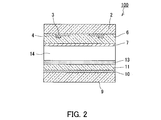
- FIG. 2 is a longitudinal sectional view of the PDP 100 (a sectional view taken along line II in FIG. 1).
- the PDP 100 includes a front plate (first panel) 1 and a back plate (second panel) 8.
- a discharge space 14 is formed between the front panel 1 and the back panel 8.
- This PDP 100 is an AC surface discharge type, and has the same configuration as the PDP according to the conventional example except that the protective layer 7 is formed of the above-described compound.
- the front plate 1 includes a front glass substrate (first substrate) 2 and a display electrode (first electrode) composed of a transparent conductive film 3 and a bus electrode 4 formed on an inner side surface (a surface facing the discharge space 14). 5, a dielectric layer (first dielectric layer) 6 formed to cover the display electrode 5, and a protective layer 7 formed on the dielectric layer 6.
- the display electrode 5 is formed by laminating a bus electrode 4 made of Ag or the like on a transparent conductive film 3 made of ITO or tin oxide in order to ensure good conductivity.
- the back plate 8 includes a back glass substrate (second substrate) 9, an address electrode (second electrode) 10 formed on one surface thereof, and a dielectric layer (second electrode) formed so as to cover the address electrode 10. (Dielectric layer) 11, barrier ribs 12 provided on the upper surface of the dielectric layer 11, and a phosphor layer formed between the barrier ribs 12.
- the phosphor layers are formed so that the red phosphor layer 13 (R), the green phosphor layer 13 (G), and the blue phosphor layer 13 (B) are arranged in this order.
- BaMgAl 10 O 17 : Eu is used as a blue phosphor
- Zn 2 SiO 4 : Mn is used as a green phosphor
- Y 2 O 3 : Eu is used as a red phosphor. it can.
- the front plate 1 and the back plate 8 are arranged so that the longitudinal directions of the display electrodes 5 and the address electrodes 10 are orthogonal to each other and face each other, and are joined using a sealing member (not shown).
- the discharge space 14 is filled with a discharge gas composed of a rare gas component such as He, Xe, or Ne.
- the display electrode 5 and the address electrode 10 are each connected to an external drive circuit (not shown), and a discharge is generated in the discharge space 14 by a voltage applied from the drive circuit, and a short wavelength (wavelength generated by the discharge).
- the phosphor layer 13 is excited by ultraviolet rays of 147 nm and emits visible light.
- the protective layer 7 the electron emission material described above is used.
- FIG. 3 is an exploded perspective view of the PDP 200.
- FIG. 4 is a longitudinal sectional view of the PDP 200 (a sectional view taken along line II in FIG. 3).
- the PDP 200 has the same structure as the PDP 100 except that the protective layer 7 is made of MgO and the above-described electron emission material 20 is arranged on the protective layer 7 in the form of particles. Also in the PDP 200, the electron emission material 20 faces the discharge space 14.
- the front plate 1 is produced.
- a plurality of line-shaped transparent electrodes 3 are formed on one main surface of the flat front glass substrate 2.
- the entire front glass substrate 1 is heated to fire the silver paste to form the bus electrode 4.
- the display electrode 5 is formed.
- the glass paste containing the glass for the dielectric layer 6 in the PDP 200 of the present embodiment is applied to the main surface of the front glass substrate 2 so as to cover the display electrodes 5 by a blade coater method. Thereafter, the entire front glass substrate 2 is held at 90 ° C. for 30 minutes to dry the glass paste, and then baked at a temperature of about 580 ° C. for 10 minutes.
- a magnesium oxide (MgO) film is formed on the dielectric layer 6 by an electron beam evaporation method, and is baked to form the protective layer 7.
- the firing temperature at this time is around 500 ° C.
- a paste-like material obtained by mixing a powdered electron emission material in a vehicle such as ethyl cellulose is applied by a printing method, dried, and fired at a temperature of about 500 ° C.
- a layer in which particles of the electron emission material 20 are dispersed is formed.
- the back plate 8 is produced. After applying a plurality of silver pastes in a line on one main surface of the flat back glass substrate 9, the entire back glass substrate 9 is heated and the silver paste is baked to form the address electrodes 10.
- a partition 12 is formed by applying a glass paste between adjacent address electrodes 10 and heating the entire back glass substrate 9 to fire the glass paste.
- the phosphor layer is formed by removing the resin component (binder) and the like.
- the front plate 1 and the back plate 8 thus obtained are bonded together using sealing glass.
- the temperature at this time is around 500 ° C. Thereafter, after the sealed interior is evacuated to high vacuum, a rare gas is sealed.
- PDP200 is obtained as described above.
- the electron emission material in the present invention described above is formed as a thin film instead of the protective layer 7 made of the MgO film, a normal thin film process such as electron beam evaporation may be used as appropriate, similarly to the MgO film.
- the electron emission material powder is mixed with a vehicle, a solvent, or the like to obtain a paste with a high content of the electron emission material powder, which is thinly spread by a method such as a printing method and then fired to form a thin film.
- it may be a thick film.
- Electrode emission material an electron-emitting material synthesized by reacting SnO 2 and K 2 CO 3 with CaCO 3 by a solid phase method, SnO 2 with SrCO 3 , Li 2 CO 3 , Na 2 CO 3 or K 2 CO
- Each of the electron emission materials synthesized by reacting by the solid-phase powder method shows the effect of reducing carbonate formation.
- CaCO 3 , SrCO 3 , BaCO 3 , SnO 2 , Li 2 CO 3 , Na 2 CO 3 , K 2 CO 3 , Rb 2 CO 3, and Cs 2 CO 3 of a reagent grade or higher were used. These raw materials were weighed so that the molar ratio of each metal ion was as shown in Table 1, wet-mixed using a ball mill, and then dried to obtain a mixed powder.
- the carbonation amount of each sample obtained by XPS is No. containing no alkali metal. 1, no. 5 and no. No. 11 sample, no. The value is smaller than 24 MgO. However, no. 2, no. 6, no. In Nos. 12 to 18, it was recognized that the amount of carbonation was extremely reduced as compared with the comparative examples (No. 1, No. 5, No. 11) in which no alkali metal was added, and remarkable stability due to the inclusion of the alkali metal. The conversion effect was confirmed. No. From the amount of carbonation of the samples 5 to 23, it was confirmed that the desirable value of b was 0.002 or more and 0.3 or less. In addition, it was confirmed that any alkali species of Li, Na, K, Rb, and Cs has an effect of suppressing the formation of carbonate.
- PDP PDP using an electron emission material according to the present invention with improved chemical stability is shown.
- a front glass substrate made of flat soda lime glass having a thickness of about 2.8 mm was prepared.
- an ITO (transparent electrode) material was applied in a predetermined pattern and dried.
- a plurality of silver pastes which are a mixture of silver powder and an organic vehicle, were applied in a line shape, and then the front glass substrate was heated, whereby the silver paste was baked to form display electrodes.
- a glass paste is applied to the front panel on which the display electrode is manufactured by using a blade coater method, and the glass paste is dried by holding at 90 ° C. for 30 minutes, and then baked at a temperature of 585 ° C. for 10 minutes. A 30 ⁇ m dielectric layer was formed.
- the protective layer was formed by firing at 500 ° C.
- partition walls were formed on the dielectric layer using glass paste between adjacent address electrodes.
- the partition was formed by repeating screen printing and baking.
- a phosphor paste of red (R), green (G), and blue (B) is applied to the surface of the dielectric layer exposed between the wall surfaces of the barrier ribs and the barrier ribs, and then dried and fired. Was made.
- the produced front plate and back plate were bonded at 500 ° C. using sealing glass. And after exhausting the inside of discharge space, Xe was enclosed as discharge gas, and PDP was produced.
- the discharge sustaining voltage was No. when the panel without the electron emission material in the present invention was used as a reference. In the panel where MgO powder of 24 was spread, the decrease was 6%. No. 11 in the panel sprayed with No. 11 powder. The panel sprayed with 15 powders had a 20% drop. From this result, like the PDP of the present invention, an electron emission material containing at least one element selected from the group consisting of Ca, Sr and Ba, Sn, an alkali metal, and O faces the discharge space. It was confirmed that the discharge sustaining voltage can be greatly reduced by arranging in this manner.
- the present invention can be suitably applied to a PDP that requires further reduction in power consumption.
Landscapes
- Physics & Mathematics (AREA)
- Engineering & Computer Science (AREA)
- Plasma & Fusion (AREA)
- Gas-Filled Discharge Tubes (AREA)
Abstract
Description
本実施例では、CaCO3にSnO2及びK2CO3を固相法により反応させて合成した電子放出材料と、SrCO3にSnO2と、Li2CO3、Na2CO3又はK2CO3とを固相法により反応させて合成した電子放出材料と、BaCO3にSnO2と、Li2CO3、Na2CO3、K2CO3、Rb2CO3又はCs2CO3とを、固相粉末法により反応させて合成した電子放出材料とについて、それぞれ炭酸化物形成の低減効果を示す。

本実施例では、化学的安定性が改善された本発明における電子放出材料を用いたPDPについて示す。厚さ約2.8mmの平坦なソーダライムガラスからなる前面ガラス基板を用意した。この前面ガラス基板の面上に、ITO(透明電極)の材料を所定のパターンで塗布し、乾燥した。次いで、銀粉末と有機ビヒクルとの混合物である銀ペーストをライン状に複数本塗布した後、上記前面ガラス基板を加熱することにより、上記銀ペーストを焼成して表示電極を形成した。
Claims (8)
- 第1のパネルと第2のパネルとを含み、前記第1のパネルと前記第2のパネルとの間に放電空間が形成されているプラズマディスプレイパネルであって、
前記放電空間に面するように電子放出材料が配置されており、
前記電子放出材料が、Ca、Sr及びBaからなる群より選ばれる少なくとも1種の元素と、Snと、アルカリ金属と、O(酸素)とを含む、プラズマディスプレイパネル。 - 前記電子放出材料は、一般式a(M1O)・SnO2・b(M2O0.5)(式中のM1はCa、Sr及びBaからなる群より選ばれる少なくとも1種の元素であり、M2はLi、Na、K、Rb及びCsからなる群より選ばれる少なくとも1種の元素である。aの値は1以上2以下の範囲であり、bの値は0.002以上0.3以下の範囲である。)で表される、請求項1に記載のプラズマディスプレイパネル。
- 前記第1のパネルは、第1の基板と、前記第1の基板上に形成された第1の電極と、前記第1の電極を覆う第1の誘電体層とを含み、
前記第2のパネルは、第2の基板と、前記第2の基板上に形成された第2の電極と、前記第2の電極を覆う第2の誘電体層と、蛍光体層とを含み、
前記電子放出材料は、前記第1のパネル及び前記第2のパネルから選ばれる少なくとも1つのパネル上に、前記放電空間に面するように配置されている、請求項1に記載のプラズマディスプレイパネル。 - 前記電子放出材料が、粒子及び膜から選ばれる少なくとも1つの形態で配置されている、請求項3に記載のプラズマディスプレイパネル。
- 前記第1の誘電体層上に保護層が形成されている、請求項3に記載のプラズマディスプレイパネル。
- 前記保護層がMgOからなる、請求項5に記載のプラズマディスプレイパネル。
- 前記電子放出材料が粒子及び膜から選ばれる少なくとも1つの形態で、前記保護層上に配置されている、請求項5に記載のプラズマディスプレイパネル。
- 前記保護層が前記電子放出材料を含む、請求項5に記載のプラズマディスプレイパネル。
Priority Applications (2)
| Application Number | Priority Date | Filing Date | Title |
|---|---|---|---|
| US12/678,412 US8169143B2 (en) | 2008-07-25 | 2009-07-22 | Plasma display panel having electron emitting material |
| JP2010521604A JP4607255B2 (ja) | 2008-07-25 | 2009-07-22 | プラズマディスプレイパネル |
Applications Claiming Priority (2)
| Application Number | Priority Date | Filing Date | Title |
|---|---|---|---|
| JP2008192602 | 2008-07-25 | ||
| JP2008-192602 | 2008-07-25 |
Publications (1)
| Publication Number | Publication Date |
|---|---|
| WO2010010698A1 true WO2010010698A1 (ja) | 2010-01-28 |
Family
ID=41570167
Family Applications (1)
| Application Number | Title | Priority Date | Filing Date |
|---|---|---|---|
| PCT/JP2009/003446 Ceased WO2010010698A1 (ja) | 2008-07-25 | 2009-07-22 | プラズマディスプレイパネル |
Country Status (3)
| Country | Link |
|---|---|
| US (1) | US8169143B2 (ja) |
| JP (1) | JP4607255B2 (ja) |
| WO (1) | WO2010010698A1 (ja) |
Cited By (2)
| Publication number | Priority date | Publication date | Assignee | Title |
|---|---|---|---|---|
| EP2703598A1 (en) | 2012-08-27 | 2014-03-05 | S.P.C.M. Sa | Centre for the preparation of additives for hydraulic fracturing operations and hydraulic fracturing process employing the preparation centre |
| EP3159390A1 (en) | 2015-10-21 | 2017-04-26 | S.P.C.M. Sa | Composition in particulate form comprising a polymer and a proppant useful for hydraulic fracturing operation |
Citations (3)
| Publication number | Priority date | Publication date | Assignee | Title |
|---|---|---|---|---|
| JP2003016949A (ja) * | 2001-04-27 | 2003-01-17 | Matsushita Electric Ind Co Ltd | プラズマディスプレイパネル及びその製造方法 |
| JP2004273158A (ja) * | 2003-03-05 | 2004-09-30 | Noritake Co Ltd | 放電表示装置の保護膜材料 |
| JP2007095436A (ja) * | 2005-09-28 | 2007-04-12 | Matsushita Electric Ind Co Ltd | プラズマディスプレイパネル |
Family Cites Families (2)
| Publication number | Priority date | Publication date | Assignee | Title |
|---|---|---|---|---|
| JPS5263663A (en) | 1975-11-19 | 1977-05-26 | Fujitsu Ltd | Gas electric discharge panel |
| JP2007184264A (ja) * | 2006-01-04 | 2007-07-19 | Lg Electronics Inc | プラズマディスプレイパネル及びその製造方法 |
-
2009
- 2009-07-22 WO PCT/JP2009/003446 patent/WO2010010698A1/ja not_active Ceased
- 2009-07-22 US US12/678,412 patent/US8169143B2/en not_active Expired - Fee Related
- 2009-07-22 JP JP2010521604A patent/JP4607255B2/ja not_active Expired - Fee Related
Patent Citations (3)
| Publication number | Priority date | Publication date | Assignee | Title |
|---|---|---|---|---|
| JP2003016949A (ja) * | 2001-04-27 | 2003-01-17 | Matsushita Electric Ind Co Ltd | プラズマディスプレイパネル及びその製造方法 |
| JP2004273158A (ja) * | 2003-03-05 | 2004-09-30 | Noritake Co Ltd | 放電表示装置の保護膜材料 |
| JP2007095436A (ja) * | 2005-09-28 | 2007-04-12 | Matsushita Electric Ind Co Ltd | プラズマディスプレイパネル |
Cited By (3)
| Publication number | Priority date | Publication date | Assignee | Title |
|---|---|---|---|---|
| EP2703598A1 (en) | 2012-08-27 | 2014-03-05 | S.P.C.M. Sa | Centre for the preparation of additives for hydraulic fracturing operations and hydraulic fracturing process employing the preparation centre |
| US9328599B2 (en) | 2012-08-27 | 2016-05-03 | S.P.C.M. Sa | Centre for the preparation of additives for hydraulic fracturing operations and hydraulic fracturing process employing the preparation centre |
| EP3159390A1 (en) | 2015-10-21 | 2017-04-26 | S.P.C.M. Sa | Composition in particulate form comprising a polymer and a proppant useful for hydraulic fracturing operation |
Also Published As
| Publication number | Publication date |
|---|---|
| US8169143B2 (en) | 2012-05-01 |
| JPWO2010010698A1 (ja) | 2012-01-05 |
| US20100259158A1 (en) | 2010-10-14 |
| JP4607255B2 (ja) | 2011-01-05 |
Similar Documents
| Publication | Publication Date | Title |
|---|---|---|
| WO2009081589A1 (ja) | プラズマディスプレイパネル | |
| JP4607255B2 (ja) | プラズマディスプレイパネル | |
| JP4860555B2 (ja) | プラズマディスプレイパネルおよびその製造方法 | |
| JP2012009368A (ja) | プラズマディスプレイパネル | |
| WO2011118162A1 (ja) | プラズマディスプレイパネルの製造方法 | |
| WO2011118152A1 (ja) | プラズマディスプレイパネルの製造方法 | |
| WO2010143345A1 (ja) | プラズマディスプレイパネル | |
| WO2011064959A1 (ja) | プラズマディスプレイパネル | |
| JPWO2011021327A1 (ja) | プラズマディスプレイパネル | |
| JP2004273158A (ja) | 放電表示装置の保護膜材料 | |
| JP2010267402A (ja) | プラズマディスプレイパネル | |
| JP5212553B2 (ja) | プラズマディスプレイパネル | |
| WO2011118164A1 (ja) | プラズマディスプレイパネルの製造方法 | |
| JP2010033813A (ja) | プラズマディスプレイパネル | |
| US20110198985A1 (en) | Crystalline compound, manufacturing method therefor and plasma display panel | |
| JP2010033807A (ja) | プラズマディスプレイパネル | |
| WO2011118165A1 (ja) | プラズマディスプレイパネルの製造方法 | |
| WO2010089953A1 (ja) | プラズマディスプレイパネル | |
| JP2011086426A (ja) | プラズマディスプレイパネル | |
| JP2013037798A (ja) | プラズマディスプレイパネルおよびその製造方法 | |
| JP2011192501A (ja) | プラズマディスプレイパネル | |
| WO2011118154A1 (ja) | プラズマディスプレイパネルの製造方法 | |
| JP2013037797A (ja) | プラズマディスプレイパネルおよびその製造方法 |
Legal Events
| Date | Code | Title | Description |
|---|---|---|---|
| ENP | Entry into the national phase |
Ref document number: 2010521604 Country of ref document: JP Kind code of ref document: A |
|
| WWE | Wipo information: entry into national phase |
Ref document number: 12678412 Country of ref document: US |
|
| 121 | Ep: the epo has been informed by wipo that ep was designated in this application |
Ref document number: 09800214 Country of ref document: EP Kind code of ref document: A1 |
|
| NENP | Non-entry into the national phase |
Ref country code: DE |
|
| 122 | Ep: pct application non-entry in european phase |
Ref document number: 09800214 Country of ref document: EP Kind code of ref document: A1 |