WO2010010609A1 - コンタクトホールの形成方法、及び回路基板 - Google Patents
コンタクトホールの形成方法、及び回路基板 Download PDFInfo
- Publication number
- WO2010010609A1 WO2010010609A1 PCT/JP2008/063138 JP2008063138W WO2010010609A1 WO 2010010609 A1 WO2010010609 A1 WO 2010010609A1 JP 2008063138 W JP2008063138 W JP 2008063138W WO 2010010609 A1 WO2010010609 A1 WO 2010010609A1
- Authority
- WO
- WIPO (PCT)
- Prior art keywords
- contact hole
- conductive
- photosensitive resin
- forming
- insulating film
- Prior art date
- Legal status (The legal status is an assumption and is not a legal conclusion. Google has not performed a legal analysis and makes no representation as to the accuracy of the status listed.)
- Ceased
Links
Images



Classifications
-
- H—ELECTRICITY
- H05—ELECTRIC TECHNIQUES NOT OTHERWISE PROVIDED FOR
- H05K—PRINTED CIRCUITS; CASINGS OR CONSTRUCTIONAL DETAILS OF ELECTRIC APPARATUS; MANUFACTURE OF ASSEMBLAGES OF ELECTRICAL COMPONENTS
- H05K3/00—Apparatus or processes for manufacturing printed circuits
- H05K3/40—Forming printed elements for providing electric connections to or between printed circuits
- H05K3/4038—Through-connections; Vertical interconnect access [VIA] connections
- H05K3/4053—Through-connections; Vertical interconnect access [VIA] connections by thick-film techniques
- H05K3/4069—Through-connections; Vertical interconnect access [VIA] connections by thick-film techniques for via connections in organic insulating substrates
-
- H—ELECTRICITY
- H05—ELECTRIC TECHNIQUES NOT OTHERWISE PROVIDED FOR
- H05K—PRINTED CIRCUITS; CASINGS OR CONSTRUCTIONAL DETAILS OF ELECTRIC APPARATUS; MANUFACTURE OF ASSEMBLAGES OF ELECTRICAL COMPONENTS
- H05K3/00—Apparatus or processes for manufacturing printed circuits
- H05K3/46—Manufacturing multilayer circuits
- H05K3/4644—Manufacturing multilayer circuits by building the multilayer layer by layer, i.e. build-up multilayer circuits
- H05K3/4647—Manufacturing multilayer circuits by building the multilayer layer by layer, i.e. build-up multilayer circuits by applying an insulating layer around previously made via studs
-
- H—ELECTRICITY
- H05—ELECTRIC TECHNIQUES NOT OTHERWISE PROVIDED FOR
- H05K—PRINTED CIRCUITS; CASINGS OR CONSTRUCTIONAL DETAILS OF ELECTRIC APPARATUS; MANUFACTURE OF ASSEMBLAGES OF ELECTRICAL COMPONENTS
- H05K2203/00—Indexing scheme relating to apparatus or processes for manufacturing printed circuits covered by H05K3/00
- H05K2203/05—Patterning and lithography; Masks; Details of resist
- H05K2203/0502—Patterning and lithography
- H05K2203/0514—Photodevelopable thick film, e.g. conductive or insulating paste
-
- H—ELECTRICITY
- H05—ELECTRIC TECHNIQUES NOT OTHERWISE PROVIDED FOR
- H05K—PRINTED CIRCUITS; CASINGS OR CONSTRUCTIONAL DETAILS OF ELECTRIC APPARATUS; MANUFACTURE OF ASSEMBLAGES OF ELECTRICAL COMPONENTS
- H05K2203/00—Indexing scheme relating to apparatus or processes for manufacturing printed circuits covered by H05K3/00
- H05K2203/05—Patterning and lithography; Masks; Details of resist
- H05K2203/0548—Masks
- H05K2203/0551—Exposure mask directly printed on the PCB
-
- H—ELECTRICITY
- H05—ELECTRIC TECHNIQUES NOT OTHERWISE PROVIDED FOR
- H05K—PRINTED CIRCUITS; CASINGS OR CONSTRUCTIONAL DETAILS OF ELECTRIC APPARATUS; MANUFACTURE OF ASSEMBLAGES OF ELECTRICAL COMPONENTS
- H05K2203/00—Indexing scheme relating to apparatus or processes for manufacturing printed circuits covered by H05K3/00
- H05K2203/11—Treatments characterised by their effect, e.g. heating, cooling, roughening
- H05K2203/1173—Differences in wettability, e.g. hydrophilic or hydrophobic areas
Definitions
- the present invention relates to a contact hole forming method and a circuit board.
- a contact hole is one of the wirings connecting elements such as transistors and capacitors formed on a circuit board.
- a conventional typical method for forming a contact hole is a method as disclosed in Patent Document 1. That is, as shown in FIG. 4A, the insulating film 11 is formed on the substrate 1 on which the metal thin film to be the lower electrode 10 is formed, and the resist film 12 is formed on the insulating film 11. Then, as shown in FIG. 4B, an opening for forming a contact hole is formed in the resist film 12 by a photolithography technique, and reactive gas etching, reactive ion etching, or the like is performed using the resist film 12 as a mask. By performing etching or ashing with oxygen plasma, the insulating film 11 is selectively removed to form the holes 13.
- a conductive portion 14 is formed in the hole by a vacuum process such as sputtering, the resist film 12 is removed, and then a metal thin film that becomes the upper electrode 15 is formed on the insulating film 11.
- a contact hole is formed by forming.
- the conductive material is injected into the hole 13 formed by etching or ashing in place of the above-described vacuum process, such as a method of plating after forming a conductive polymer, or a method of pouring the conductive polymer into the hole 13. It can also be formed by a wet process (see, for example, Patent Document 2).
- the conventional method includes an etching process and an ashing process, there is a problem that an expensive apparatus is required and a large number of substrates cannot be processed at a time.
- these devices consume a large amount of power, and it is difficult to say that they are desirable steps in the recent call for CO 2 reduction.
- an organic transistor uses an organic material as a material for an insulating film (gate insulating film) and a semiconductor layer, and thus has an advantage that a circuit can be formed by a simple method such as a wet process. If it is included, the advantages of the organic transistor that can be manufactured only by the wet process are offset.
- a method of forming the hole 13 without performing etching or ashing has been studied. Specifically, this is a method of forming a hole 13 in the insulating film 11 by a photolithography technique using a photosensitive material for the insulating film 11.
- an undesired component such as a photoinitiator or the like as a gate insulating film of the transistor is included, and thus desired insulating characteristics may not be obtained.
- an object of the present invention is to provide a contact hole forming method capable of forming a contact hole structure wiring by a simple wet process, and to provide a circuit board having a contact hole.
- Another object of the present invention is to overcome the conventional common sense of forming a hole in an insulating film and injecting a conductive material, and to form a novel contact hole forming method in which a conductive portion of a contact hole is formed first, and
- An example is to provide a circuit board having contact holes.
- Another object of the present invention is to provide a contact hole forming method suitable for a circuit board having an organic transistor as an element, and a circuit board having a contact hole connected to the organic transistor, as an example. .
- the contact hole forming method is a contact hole forming method for connecting a first conductive member and a second conductive member arranged via an insulating film as described in claim 1.
- Special features including To.
- a circuit board according to the present invention is a circuit board including a contact hole for connecting a first conductive member and a second conductive member arranged via an insulating film as described in claim 12.
- the conductive portion of the contact hole is formed of a liquid repellent photosensitive resin containing a conductive material or a photosensitive resin mixed with a liquid repellent component.
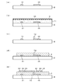
- FIG. 6 is a process diagram in which contact holes are formed according to a preferred embodiment of the present invention. It is a figure which shows the formation method of the contact hole by a conventional method.
- FIG. 1 and FIG. 2 show a circuit board 2 for an organic EL display device.
- FIG. 1 shows a plan view and a side view (portion of an organic transistor) of the circuit board 2
- FIG. 2 shows a circuit diagram.
- the circuit board 2 includes two organic transistors (Tr1) 3 and (Tr2) 4 (for example, organic TFT) and an organic EL (electroluminescence) element 5 (light emitting element) (for example, an OLED or the like) and a charge holding capacitor (Cap) 6 (for example, a storage capacitor or the like) are formed to form a dot of the display device.
- a display area is configured by arranging a large number of dots in a matrix.
- the organic transistor 3 is a switching transistor
- the organic transistor 4 is a driving transistor.
- These elements formed on the circuit board 2 form a circuit as shown in FIG. 2 and are configured to actively drive the organic EL element 5. Note that the arrangement of each element shown in FIG. 1 is described as an example, and is not limited to this arrangement.
- the gate electrode 31 of the switching organic transistor 3 is connected to the scan line (Vscan), and the source electrode 32 is connected to the data line (Vdata). Further, the drain electrode 33 is connected to the gate electrode 41 of the driving organic transistor 4 and to one terminal of the capacitor 6 of the capacitance line (Vcap).
- the source electrode 42 of the driving organic transistor 4 is connected to the low potential side power supply line (Vss). Furthermore, the anode terminal of the organic EL element 5 is connected to the drain electrode 43 of the organic transistor 4 for driving.
- reference numerals 34 and 44 in FIG. 1 denote organic semiconductor layers.
- a contact hole 7 as shown in FIG. 1B is formed in the insulating film (gate insulating film) 8.
- a liquid repellent photosensitive resin containing a conductive material or a mixture of a liquid repellent component mixed with a photosensitive resin containing a conductive material is used as a material for forming the conductive portion of the contact hole 7.
- the said photosensitive resin is apply
- the insulating film 8 is also formed by the wet process, thereby realizing the formation of the contact hole structure in the reverse order. .
- any one of a conductive nanotube, metal fine particles, and a conductive polymer, or a mixture of two or more types can be used.
- the conductive nanotube only needs to have conductivity, and the size and type thereof are not particularly limited.
- a carbon nanotube is preferable.
- the structure may be either a single layer structure or a multilayer structure, and may be either a structure with a closed tip or an open structure.
- a conductor or a semiconductor may be used.
- a preferable blending ratio of the conductive nanotubes is 1 to 50% by mass, preferably 1 to 25% by mass. Since the nanotubes have an elongated shape, there is an advantage that the contact rate between the nanotubes in the photosensitive resin is increased and it is easy to ensure conduction.
- the type of metal fine particles is not particularly limited as long as it is conductive metal fine particles.
- Preferable examples include fine particles of any one of Ag, Au, Cu, Cr, Fe, Zn, Al, Pt, ZuO, SnO, IZO, and ITO, or a mixture of two or more fine particles.
- the size of the metal fine particles is not particularly limited, but is preferably fine to ensure conduction, and it is preferable to use nanoparticles or microparticles. More preferred are fine particles having a particle size of 1 to 100 nm.
- a preferable blending ratio of metal fine particles that can provide sufficient conduction and can be patterned can be 50 to 90% by mass.
- the type of the conductive polymer is not particularly limited as long as it is a conductive polymer.
- Preferred conductive polymers include conjugated polymer compounds such as PEDOT / PSS, polyacetylene, polyparaphenylene, polyaniline, polythiophene, and polyparaphenylene vinylene. Further, a preferable blending ratio of the conductive polymer can be 50 to 90% by mass.
- a photoresist As the photosensitive resin containing (dispersing) the above-described conductive material, a photoresist can be cited as an example.
- the photosensitive property may be either positive or negative, and a chemically amplified resist can also be used.
- the resin is not particularly limited as long as it can form a pattern by being exposed to light.
- Preferable examples include acrylic resin, epoxy resin, polyimide resin and the like.
- the photosensitive resin used for this embodiment has a liquid-repellent property.
- liquid repellent photosensitive resin having a liquid repellent molecule such as a fluorine component in the molecular structure of the photosensitive resin, or a photosensitive resin mixed with a liquid repellent component such as a fluorine component.
- a liquid repellent photosensitive material containing a conductive material is mixed by mixing a large number of conductive materials in a solvent in which a liquid repellent photosensitive resin or a photosensitive resin mixed with a liquid repellent component is dissolved. You may make it prepare the mixture which mixed the liquid repellent component with resin or the photosensitive resin containing an electroconductive material. Of course, it may be prepared by other methods.
- the type of the solvent is not particularly limited, and an example is propylene glycol monomethyl ether acetate (PGMEA).
- PMEA propylene glycol monomethyl ether acetate
- the conductive material and the photosensitive resin, and in the case of further addition, the liquid repellent component may be used as a main component, and the addition of other components is not limited.
- a dispersant for suppressing aggregation of the fine particles can be added.
- One example thereof is modifying the surface of the fine particles with a thiol compound or a silane coupling agent.
- the material of the insulating film used in this embodiment may be formed by a wet process such as a coating method, and any insulating material can be used as long as this condition is satisfied.
- a wet process such as a coating method
- any insulating material can be used as long as this condition is satisfied.
- preferred examples include an aqueous solution containing polyvinyl alcohol (PVA), a PGMEA solution of polyvinyl phenol, and the like.
- FIG. 3 schematically shows a cross section of the substrate in the main process.
- a lower electrode is formed as a first conductive member on the substrate 2.
- the gate electrodes (31, 41) of the organic transistors 3 and 4 are formed.
- the lower electrode, the scan line, and the capacitance line of the capacitor 6 can be formed in this step.
- the electrode forming method include a sputtering method and an electroless plating method. However, it is not limited to this, and any film forming method may be used.
- the electrode material is not particularly limited, but as an example, Pt, Au, W, Ru, Ir, Al, Sc, Ti, V, Mn, Fe, Co, Ni, Zn, Ga, Y, Zr Nb, Mo, Tc, Rh, Pd, Ag, Cd, Ln, Sn, Ta, Re, Os, Tl, Pb, La, Ce, Pr, Nd, Pm, Sm, Eu, Gd, Tb, Dy, Ho , Er, Tm, Yb, Lu and other metal or combinations thereof, organic conductive materials including conjugated polymer compounds such as metal oxides such as ITO and IZO, polyanilines, polythiophenes and polypyrroles be able to.
- the substrate 2 include a glass substrate and a plastic substrate.
- a liquid-repellent photosensitive material containing a conductive material on the substrate 2 on which the gate electrodes (31, 41) are formed that is, a base surface on which a conductive portion is formed.
- a mixture of a resin or a photosensitive resin containing a conductive material mixed with a liquid repellent component is applied and dried to form a coating film 71.
- a known resist is applied on the coating film 71 and dried to form a resist film 9.
- An example of the coating method is a spin coating method. However, it is not limited to this, and any coating method may be used.
- an opening 91 of the resist film 9 is formed at a position where a conductive portion of the contact hole is to be formed.
- a known photolithography method such as electron beam drawing can be employed.
- the resist film 9 in which the opening 91 is formed is used as a mask to irradiate light to the lower layer film 71 and develop the conductive film at a position corresponding to the opening 91.
- a conductive portion 72 made of a liquid repellent photosensitive resin containing a conductive material or a mixture of a liquid repellent component mixed with a photosensitive resin containing a conductive material is formed.
- a baking process is performed by heating at a temperature corresponding to the type of resin, and the resin of the conductive portion 72 is cured.
- the film 71 can be irradiated with light by using a light source such as ultra-high pressure mercury as an example.
- the substrate 2 on which the conductive portion 71 and the gate electrodes (31, 41) are formed that is, the ground surface on which the conductive portion and the first conductive member are formed.
- an insulating material for example, 10% aqueous solution of PVA
- the insulating film 8 can be a dielectric of the capacitor 6 as well as the gate insulating films of the transistors 3 and 4.
- the insulating material is not limited to PVA, and other polymers having insulating properties can also be used.
- the coating method include spin coating and the like. However, it is not limited to this, and any coating method may be used.
- an upper electrode as a second conductive member is formed on the insulating film 8.
- the source electrodes (32, 42) and drain electrodes (42, 43) of the organic transistors 3 and 4; the upper electrode of the capacitor 6 (not shown); the data line and the power line; Wires to be connected are formed in a lump.
- the electrode forming method include a sputtering method and an electroless plating method. However, it is not limited to this, and any film forming method may be used. Further, the electrode material is not particularly limited, and the same material as the above-described gate electrode can be used. In the example of FIG. 3, the electrodes and wirings are formed in a lump in order to simplify the process, but each electrode or wiring may be formed in a separate process.
- the channel portions of the source electrode (32, 42) and the drain electrode (33, 43) for example, poly-3-hexylthiophene (P3HT), poly [9,9-dioctylfluorene-co-bithiophene]
- An organic semiconductor material such as (F8T2) is applied and dried to form the organic semiconductor layers (34, 44).
- the organic semiconductor material may be applied by an inkjet method.
- the bank may be formed so as to surround a region where the organic semiconductor material is applied.
- the lower electrode, the organic EL layer, and the upper electrode of the organic EL element 5 are sequentially formed at predetermined positions and sealed with an inorganic material. Through such steps, the circuit board 2 for the organic EL display device having the organic transistors 3 and 4 is formed.
- the liquid repellent photosensitive resin containing a fine conductive material or the photosensitive resin containing a fine conductive material as a material for forming the conductive portion 72 of the contact hole 7 is liquid repellent.
- the mixture in which the components are mixed to form a coating film 71 on the substrate 2 and patterning by irradiating light it is possible to form a conductive portion 72 having a desired size at a desired position.
- the insulating film 8 is similarly formed by the wet process. Wiring can be formed.
- power consumption can be reduced by the amount corresponding to the elimination of the etching and ashing steps, which can contribute to the reduction of CO 2 emissions.
- the upper surface and the periphery of the conductive portion 72 can be prevented from being covered with an insulating material. If the upper surface of the conductive portion 72 is covered with an insulating material, an insulating material is interposed between the upper electrode and the conductive material 72, and sufficient conduction may not be obtained. Therefore, in the present embodiment, by using a photosensitive resin having liquid repellency, the upper surface of the conductive portion 72 is prevented from being covered with an insulating material.
- the conductive portion 72 of the contact hole 7 is formed first, and then the insulating film 8 is formed, thereby preventing problems due to thermal contraction of the conductive portion 72 formed by the wet process. It becomes possible. That is, when a hole is formed in the insulating film in accordance with the conventional method and a conductive material is injected into the hole by a wet process to form the conductive portion 72, the conductive portion 72 is thermally shrunk by drying or baking, and the hole is formed in the hole. In some cases, a cavity is formed, or the upper surface of the conductive portion 72 is lower than the surface of the insulating film.
- the wiring of the contact hole structure can be formed by a series of wet processes. Therefore, this method is applied to the formation of a circuit substrate having an organic transistor, and can be manufactured by a simple method such as a wet process. It is possible to take advantage of the organic transistor fabrication aspect that it is possible. That is, the contact hole forming method according to the present embodiment is suitable for forming a circuit board having an organic transistor.
- the conductive portion 72 is formed by the process shown in FIG. 3C, and then a sintering process is performed to remove the metal fine particles in the conductive portion 72.
- a sintering process is performed to remove the metal fine particles in the conductive portion 72.
- the temperature for sintering varies depending on the type of metal, but it is usually an example that the temperature is about 80% of the melting temperature of the metal. For example, in the case of Ag, the temperature is 200 to 250 ° C. Except for performing the sintering treatment, the other steps can be performed in the same manner as in the above-described embodiment. Thus, by performing the sintering process, it becomes possible to ensure conduction more reliably.
- UV treatment or a combination of UV treatment and ozone treatment is performed, so that all or one of the organic substances contained in the conductive portion 72 is obtained.
- the part may be disassembled and removed.
- the circuit board 2 for an organic EL display device as shown in FIG. 1 is taken as an example.
- the circuit board 2 is not limited to this, and a liquid crystal display or electronic paper is used.
- a circuit board having an organic transistor such as a general circuit board as shown in FIG. That is, the contact hole forming method according to the present embodiment can be applied to all substrates having contact holes.
- a contact hole structure wiring is formed.
- a liquid repellent photosensitive resin containing a conductive material, or a liquid repellent component in a photosensitive resin containing a conductive material can also be used as a wiring material other than contact holes. In this case, it does not necessarily have liquid repellency.
- a top contact type organic transistor is described, but the structure is not limited to this structure.
- a bottom contact type or top gate type organic transistor may be used.
- it is not necessarily an organic transistor and may be an inorganic transistor.
- a mixture of Ag particles in a fluorine-containing acrylic photoresist was applied by spin coating on a glass substrate on which a transistor electrode and a capacitor electrode pattern were formed.
- the unexposed portion was removed and baked at 220 ° C. to form a conductive portion.
- a polyvinyl alcohol (PVA) 10% aqueous solution was applied to the glass substrate by spin coating as an insulating film material. Since the conducting portion was water-repellent, no PVA remained on the upper surface of the conducting portion.
- an electrode was produced by sputtering to ensure conduction between the transistors and form a circuit.
Landscapes
- Engineering & Computer Science (AREA)
- Manufacturing & Machinery (AREA)
- Microelectronics & Electronic Packaging (AREA)
- Thin Film Transistor (AREA)
- Internal Circuitry In Semiconductor Integrated Circuit Devices (AREA)
Abstract
【課題】コンタクトホール構造の配線を簡易なウエットプロセスによって形成する 【解決手段】第1の導電性部材(31,41)が形成された下地面(2)に、導電性材料を含有する撥液性感光樹脂又は撥液性成分を混合した感光樹脂を塗布して塗膜(71)を形成し、フォトリソグラフィ法によって塗膜(71)をパターニングして、コンタクトホールの導通部分(72)を形成する。その後、コンタクトホールの導通部分(72)及び第1の導電性部材(31,41)が形成された下地面に、絶縁性材料を塗布して絶縁膜(8)を形成し、最後に絶縁膜(8)上に第2の導電性部材(32,33,42,43)を形成する。
Description
本発明は、コンタクトホールの形成方法、及び回路基板に関する。
回路基板上に形成されるトランジスタやコンデンサなどの素子間を接続する配線の一つにコンタクトホールがある。従来の典型的なコンタクトホールの形成方法は、特許文献1に開示されているような方法である。すなわち、図4(a)に示すように、下部電極10となる金属薄膜が形成された基板1に絶縁膜11を形成し、絶縁膜11上にレジスト膜12を形成する。そして、図4(b)に示すように、フォトリソグラフィ技術によりコンタクトホール形成用の開口部をレジスト膜12に形成し、このレジスト膜12をマスクにして反応性ガスエッチングや反応性イオンエッチングなどのエッチング或いは酸素プラズマによるアッシングを行うことにより、絶縁膜11を選択的に除去してホール13を形成する。続いて、図4(c)に示すように、スパッタなどの真空プロセスによりホール内に導通部分14を形成し、レジスト膜12を除去した後、絶縁膜11上に上部電極15となる金属薄膜を形成することによってコンタクトホールを形成する。
また、エッチングやアッシングにより形成したホール13への導電性材料の注入は、前述の真空プロセスに代えて、導電性ポリマーを形成した後にメッキをする方法や、導電性ポリマーをホール13に流し込む方法など、ウエットプロセスにより形成することもできる(例えば、特許文献2参照)。
しかしながら、従来の方法は、エッチングプロセスやアッシングプロセスを含むため、高価な装置を必要とし、また一度に大量の基板を処理することができないという問題があった。また、これらの装置は消費電力が大きく、さらに近年のCO2削減が叫ばれている中においては、望ましい工程であるとは言い難い。
さらに、前述のエッチングやアッシングなどのドライプロセスを含む従来の方法では、近年注目されている有機トランジスタを用いて回路基板を形成する場合に、有機トランジスタの製作面における利点を相殺してしまう問題がある。すなわち、有機トランジスタは、絶縁膜(ゲート絶縁膜)及び半導体層の材料に有機物を使用するので、ウエットプロセスといった簡易な方法で回路を形成可能という利点があるが、従来方法のようにドライプロセスが含まれていると、ウエットプロセスだけで製作可能な有機トランジスタの利点が相殺されてしまう。
なお、従来においても、エッチングやアッシングを行わずにホール13を形成する方法が検討されている。具体的には、絶縁膜11に感光性材料を用いて、フォトリソグラフィ技術によって絶縁膜11にホール13を形成する方法である。しかしながら、この場合、光開始剤など、トランジスタのゲート絶縁膜として好ましくない成分が含まれることとなり、そのため所望の絶縁特性が得られない場合がある。
本発明が解決しようとする課題には、上述した問題が一例として挙げられる。そこで、本発明の目的としては、コンタクトホール構造の配線を簡易なウエットプロセスによって形成することのできるコンタクトホールの形成方法、及びコンタクトホールを有する回路基板を提供することが一例として挙げられる。
また本発明の他の目的は、絶縁膜にホールを形成して導電性材料を注入するという従来の常識を覆し、コンタクトホールの導通部分を先に形成するという新規なコンタクトホールの形成方法、及びコンタクトホールを有する回路基板を提供することが一例として挙げられる。
さらに本発明の他の目的は、特に、有機トランジスタを素子として有する回路基板に好適なコンタクトホールの形成方法、及び有機トランジスタに接続されるコンタクトホールを有する回路基板を提供することが一例として挙げられる。
本発明のコンタクトホールの形成方法は、請求項1に記載のように、絶縁膜を介して配置される第1の導電性部材と第2の導電性部材とを接続するコンタクトホールの形成方法であって、前記第1の導電性部材が形成された下地面に、導電性材料を含有する撥液性感光樹脂又は撥液性成分を混合した感光樹脂を塗布して塗膜を形成する工程と、フォトリソグラフィ法によって前記塗膜をパターニングして、前記導電性材料を含有する撥液性感光樹脂又は撥液性成分を混合した感光樹脂からなるコンタクトホールの導通部分を形成する工程と、前記コンタクトホールの導通部分及び第1の導電性部材が形成された下地面に、絶縁性材料を塗布して絶縁膜を形成する工程と、前記絶縁膜上に第2の導電性部材を形成する工程と、を含むことを特徴とする。
本発明の回路基板は、請求項12に記載のように、絶縁膜を介して配置される第1の導電性部材と第2の導電性部材とを接続するコンタクトホールを含む回路基板であって、前記コンタクトホールの導通部分が、導電性材料を含有する撥液性感光樹脂又は撥液性成分を混合した感光樹脂で形成されていることを特徴とする。
3 有機トランジスタ(Tr1)
31 ゲート電極
32 ソース電極
33 ドレイン電極
4 有機トランジスタ(Tr2)
41 ゲート電極
42 ソース電極
43 ドレイン電極
5 有機EL素子
6 キャパシタ
7 コンタクトホール
72 導通部分
8 絶縁膜
31 ゲート電極
32 ソース電極
33 ドレイン電極
4 有機トランジスタ(Tr2)
41 ゲート電極
42 ソース電極
43 ドレイン電極
5 有機EL素子
6 キャパシタ
7 コンタクトホール
72 導通部分
8 絶縁膜
本発明のコンタクトホールの形成方法及び回路基板による好ましい実施形態について、添付図面を参照しながら詳しく説明する。但し、本発明の技術的範囲は、以下に説明する実施形態によって何ら限定解釈されることはない。
本実施形態による回路基板の一例として、図1及び図2に有機EL表示装置用の回路基板2を示す。図1は、回路基板2の平面図及び側面図(有機トランジスタの部分)を示し、図2は、回路図を示す。
図1に示すように、本実施形態による回路基板2には、二つの有機トランジスタ(Tr1)3及び(Tr2)4(例えば有機TFT等)、発光素子である有機EL(エレクトロルミネッセンス)素子5(例えば、OLED等)、及び電荷保持用のキャパシタ(Cap)6(例えば、ストレージ・キャパシタ等)が形成されており、表示装置のドットを構成している。なお、実際の装置では多数のドットをマトリックス状に配列して表示領域を構成する。有機トランジスタ3は、スイッチング用のトランジスタであり、有機トランジスタ4は、ドライビング用のトランジスタである。回路基板2に形成されたこれらの素子は、図2に示すような回路を形成し、有機EL素子5をアクティブ駆動させるように構成されている。なお、図1に示す各素子の配列は一例として記載したものであり、この配列に限定されることはない。
図2に示されるように、スイッチング用の有機トランジスタ3のゲート電極31は、スキャンライン(Vscan)に接続され、ソース電極32はデータライン(Vdata)に接続されている。さらにドレイン電極33は、ドライビング用の有機トランジスタ4のゲート電極41に接続されると共に、キャパシタンスライン(Vcap)のコンデンサ6の一方の端子に接続されている。
ドライビング用の有機トランジスタ4のソース電極42は、低電位側電源ライン(Vss)に接続されている。さらにドライビング用の有機トランジスタ4のドレイン電極43には、有機EL素子5のアノード端子が接続されている。なお、図1の符号34及び44は、有機半導体層である。
上記のように、2つの有機トランジスタ3及び4を用いて、有機EL素子5をアクティブ駆動させる回路を形成する場合、有機トランジスタ3及び4とキャパシタ6の導通を確保する必要がある。そのため、図1(b)に示すようなコンタクトホール7が絶縁膜(ゲート絶縁膜)8に形成される。
本実施形態では、コンタクトホール7の導通部分を形成する材料として、導電性材料を含有する撥液性感光樹脂、又は導電性材料を含有する感光樹脂に撥液性成分を混合した混合物を用いる。そして、基板2上に前記感光樹脂を塗布して塗膜を形成し、フォトリソグラフィ法によりパターニングすることによって所望の位置に所望の大きさの導通部分を形成する。このようにウエットプロセスによって導通部分を形成した後、同じくウエットプロセスによって絶縁膜8を形成することにより、従来とは逆の順序で、コンタクトホール構造の配線を形成することを実現しているのである。
前記導電性材料としては、導電性ナノチューブ,金属微粒子,導電性高分子のいずれか一種、又は二種以上の混合物を用いることができる。
導電性ナノチューブは、導電性を有していればよく、その大きさ及び種類は特に制限されない。導電性ナノチューブとしては、カーボンナノチューブが好ましい。但し、カーボンナノチューブに制限されることはなく、金ナノチューブや白金ナノチューブのような貴金属ナノチューブを使用することができる。さらに、その構造は単層構造又は多層構造のいずれであってもよく、先端が閉じた構造又は開いた構造のいずれであってもよい。さらに導体又は半導体のいずれであってもよい。但し、導通を確保するため、直径0.5~100nmで長さが0.05~1μmのものを用いるのが好ましい。なお、感光樹脂に対して導電性ナノチューブの量が少な過ぎると充分な導通が得られない場合がある。反対に導電性ナノチューブの量が多過ぎるとフォトリソグラフィ技術によりパターニングできない場合がある。従って、導電性ナノチューブの好ましい配合比として、1~50質量%、好ましくは1~25質量%を挙げることができる。ナノチューブは細長い形状であるため、感光樹脂内でのナノチューブ同士の接触率が高められ、導通を確保し易いという利点がある。
また、金属微粒子としては、導電性を有する金属の微粒子であれば特に種類は制限されない。好ましい一例としては、Ag,Au,Cu,Cr,Fe,Zn,Al,Pt,ZuO,SnO,IZO,ITOのいずれか一種の微粒子、又は二種以上の微粒子の混合物が挙げられる。金属微粒子の大きさについても特に制限されないが、導通を確保するためには微細であることが好ましく、ナノ粒子又はマイクロ粒子を用いることが好ましい。より好ましくは粒径が1~100nmの微粒子である。なお、導電性ナノチューブと同様の理由により、充分な導通が得られ、且つ、パターニング可能な好ましい金属微粒子の配合比として、50~90質量%を挙げることができる。
また、導電性高分子としては、導電性を有する高分子であれば特に種類は制限されない。好ましい導電性高分子としては、PEDOT/PSS,ポリアセチレン,ポリパラフェニレン,ポリアニリン,ポリチオフェン,ポリパラフェニレンビニレンなどの共役性高分子化合物を挙げることができる。さらに、導電性高分子の好ましい配合比としては、50~90質量%を挙げることができる。
上記した導電性材料を含有(分散)する感光樹脂としては、フォトレジストを一例として挙げることができる。感光特性はポジ型又はネガ型のいずれであってもよく、さらに化学増幅型のレジストも使用可能である。樹脂は、光により感光してパターンを形成できるものであればよく、その種類は特に制限されない。好ましい一例として、アクリル樹脂,エポキシ樹脂,ポリイミド樹脂などを挙げることができる。さらに、詳しい理由については後述するが、本実施形態に用いる感光樹脂は、撥液特性を有しているのが好ましい。この場合、フッ素成分等の撥液性分子を感光樹脂の分子構造に有する撥液性感光樹脂、又はフッ素成分等の撥液性成分を混合した感光樹脂を用いることが好ましい。
導電性材料及び感光樹脂並びに撥液性物質は、それぞれ市販のものを使用してもよく、公知の製造方法を利用して製造するようにしてもよい。本実施形態においては、撥液性感光樹脂又は撥液性成分を混合した感光樹脂を溶解した溶媒に対して、導電性材料の多数を混合することにより、導電性材料を含有する撥液性感光樹脂、又は導電性材料を含有する感光樹脂に撥液性成分を混合した混合物を調製するようにしてもよい。勿論、他の方法で調製してもよい。
前記溶媒の種類は特に制限されないが、一例としてプロピレングリコールモノメチルエーテルアセート(PGMEA)を挙げることができる。なお、本実施形態においては、導電性材料と感光樹脂、さらに添加する場合は撥液性成分を主成分として組成されていればよく、その他の成分を添加することが制限されることはない。その他の添加成分としては、特に金属微粒子を用いた場合に、微粒子同士が凝集するのを抑制するための分散剤などを添加することができる。その一例として、チオール化合物またはシランカップリング剤等により微粒子表面を修飾することが挙げられる。
また、本実施形態に用いられる絶縁膜の材料は、塗布法などのウエットプロセスによって形成可能であればよく、この条件を満たせばいずれの絶縁性材料をも用いることができる。有機トランジスタのゲート絶縁膜を形成する場合、好ましい一例として、ポリビニルアルコール(PVA)を含有する水溶液,ポリビニルフェノールのPGMEA溶液などが挙げられる。
続いて、本実施形態に従いコンタクトホールを形成する工程を、図3を参照しながら説明する。図3には、主要な工程における基板の断面を模式的に示している。
先ず、基板2上に第1の導電性部材として下部電極を形成する。図3(a)に示す例では、有機トランジスタ3及び4のゲート電極(31,41)を形成している。さらに、図示は省略するが、キャパシタ6の下部電極、スキャンライン及びキャパシタンスラインもこの工程で形成することができる。電極の形成方法としては、スパッタリング法及び無電解メッキ法などが一例として挙げられる。但し、これに限定されることなく、いずれの成膜方法であってもよい。また、電極材料も特に制限されることはないが、一例として、Pt、Au、W、Ru、Ir、Al、Sc、Ti、V、Mn、Fe、Co、Ni、Zn、Ga、Y、Zr、Nb、Mo、Tc、Rh、Pd、Ag、Cd、Ln、Sn、Ta、Re、Os、Tl、Pb、La、Ce、Pr、Nd、Pm、Sm、Eu、Gd、Tb、Dy、Ho、Er、Tm、Yb、Lu等の金属もしくはその化合物の組み合わせ、ITO、IZOのような金属酸化物類、ポリアニリン類、ポリチオフェン類、ポリピロール類などの共役性高分子化合物を含む有機導電材料を挙げることができる。また、基板2としては、ガラス基板やプラスチック基板が一例として挙げられる。
続いて、図3(b)に示すように、ゲート電極(31,41)が形成された基板2上(すなわち、導通部分を形成する下地面)に、導電性材料を含有する撥液性感光樹脂、又は導電性材料を含有する感光樹脂に撥液性成分を混合した混合物を塗布し、乾燥させて塗膜71を形成する。次いで、塗膜71上に公知のレジストを塗布し、乾燥させてレジスト膜9を形成する。塗布方法としては、スピンコート法が一例として挙げられる。但し、これに限定されることなく、いずれの塗布方法であってもよい。さらに、図示しないフォトマスクを介して露光し、現像することにより、コンタクトホールの導通部分を形成しようとする位置に、レジスト膜9の開口部91を形成する。フォトマスクを介した露光以外にも、例えば電子線描画など、公知のフォトリソグラフィ法を採用することができる。
続いて、図3(c)に示すように、開口部91を形成したレジスト膜9をマスクにして下層の膜71に光を照射し、現像することにより、開口部91に対応する位置に導電性材料を含有する撥液性感光樹脂、又は導電性材料を含有する感光樹脂に撥液性成分を混合した混合物からなる導通部分72が形成される。こうして導通部分72が形成されると、例えば樹脂の種類に応じた温度で加熱するベーク処理を行って導通部分72の樹脂を硬化させる。膜71への光の照射は、一例として超高圧水銀などの光源を用いて行うことができる。
続いて、図3(d)に示すように、導通部分71とゲート電極(31,41)が形成された基板2上(すなわち、導通部分と第1の導電性部材が形成された下地面)に、絶縁材料(例えば、PVAの10%水溶液)を塗布し、乾燥させて絶縁膜8を形成する。この絶縁膜8は、トランジスタ3及び4のゲート絶縁膜のみならず、キャパシタ6の誘電体とすることもできる。なお、絶縁材料はPVAに限定されることはなく、絶縁性を有する他のポリマーも使用可能である。本実施形態では撥液性を有する導通部分を形成しているので、水に溶解するポリマーだけでなく、殆どのポリマーを使用することが可能である。塗布方法としては、スピンコート法などが一例として挙げられる。但し、これに限定されることなく、いずれの塗布方法であってもよい。
続いて、絶縁膜8上に、第2の導電性部材としての上部電極を形成する。図3(e)に示す例では、有機トランジスタ3及び4のソース電極(32,42)とドレイン電極(42,43)、図示しないキャパシタ6の上部電極、データライン及び電源ライン、トランジスタとキャパシタを接続する配線等を一括で形成する。電極の形成方法としては、スパッタリング法及び無電解メッキ法などが一例として挙げられる。但し、これに限定されることなく、いずれの成膜方法であってもよい。また、電極材料も特に制限されることはなく、上述したゲート電極と同様の材料を用いることができる。なお、図3の例では、工程の簡略化を図るために電極や配線を一括で形成しているが、各電極又は配線を別々の工程で形成するようにしてもよい。
最後に、ソース電極(32,42)とドレイン電極(33,43)のチャンネル部分に対して、一例としてポリ-3-ヘキシルチオフェン(P3HT),ポリ[9,9-ジオクチルフルオレン-co-ビチオフェン](F8T2)などの有機半導体材料を塗布し、乾燥させて有機半導体層(34,44)を形成する。有機半導体材料は、インクジェット法によって塗布することが一例として挙げられる。このとき、有機半導体材料を塗布する領域を囲むようにバンクを形成してもよい。また、詳しい説明は省略するが、有機EL素子5の下部電極、有機EL層、上部電極を所定の位置に順次形成し、無機材料で封止する。このような工程を通じて、有機トランジスタ3及び4を有する有機EL表示装置用の回路基板2が形成される。
上述の実施形態によれば、コンタクトホール7の導通部分72を形成する材料として、微細な導電性材料を含有する撥液性感光樹脂、又は微細な導電性材料を含有する感光樹脂に撥液性成分を混合した混合物を用い、基板2上に塗膜71を形成し、光を照射してパターニングすることにより、所望の位置に所望の大きさの導通部分72を形成することが可能となる。さらに、前述のようにウエットプロセスで導通部分72を形成した後、同じくウエットプロセスによって絶縁膜8を形成することにより、一連のウエットプロセスのみで、且つ、従来よりも工程を減らしてコンタクトホール構造の配線を形成することが可能となる。また、エッチングやアッシング工程がなくなった分だけ消費電力を低減することができ、CO2排出量削減に貢献することができる。
さらに上述の実施形態によれば、撥液特性を有する感光樹脂を用いたことにより、導通部分72を形成した基板2にPVA水溶液等の絶縁材料を塗布しても、導通部分72の上面及び周辺が絶縁材料で覆われるのを防ぐことができる。導通部分72の上面が絶縁材料で覆われてしまうと、上部電極との間に絶縁材料が介在することとなり充分な導通が得られない場合がある。そこで、本実施形態においては、撥液特性を有する感光樹脂を用いることによって、導通部分72の上面が絶縁材料で覆われてしまうことを防止している。その結果、より確実に導通を確保したコンタクトホールを形成することができる。このことは、絶縁材料で覆われていないことを確認する工程、さらに、覆われているときに除去する工程を省略することができ、簡易なプロセス工程を可能にする。
さらに上述の実施形態によれば、コンタクトホール7の導通部分72のみを先に形成し、次いで絶縁膜8を形成することによって、ウエットプロセスによって形成される導通部分72の熱収縮による不具合を防止することが可能となる。すなわち、従来方法に従って絶縁膜にホールを形成し、このホールにウエットプロセスによって導電性材料を注入して導通部分72を形成した場合、乾燥やベーク処理によって導通部分72が熱収縮し、ホール内に空洞が生じたり、導通部分72の上面が絶縁膜の表面よりも低くなったりする場合がある。しかしながら、本実施形態の場合、コンタクトホールの導通部分72のみを先に形成し、乾燥及びベーク処理した後に絶縁膜8を形成しているので、導通部分72が熱収縮することがないか、あっても収縮量は僅かである。その結果、より確実に上部電極との導通を確保することが可能となる。
さらに上述の実施形態によれば、一連のウエットプロセスによってコンタクトホール構造の配線を形成できるので、この方法を、有機トランジスタを有する回路基板の形成に適用することにより、ウエットプロセスといった簡易な方法で製作可能であるという有機トランジスタの製作面における利点を活かすことが可能となる。すなわち、本実施形態に従うコンタクトホールの形成方法は、有機トランジスタを有する回路基板の形成に好適である。
他の実施形態として、導電性材料として金属ナノ粒子を用いた場合、図3(c)に示す工程によって導通部分72を形成した後、さらに焼結処理を行って導通部分72内の金属微粒子を焼結させるようにしてもよい。焼結させるための温度は、金属の種類によって異なるが、通常、その金属の溶解温度の80%程度の温度とすることが一例として挙げられる。例えばAgの場合、200~250℃である。焼結処理を行うことを除けば、その他の工程は上述の実施形態と同様に行うことができる。このように、焼結処理を行うことで、より確実に導通を確保することが可能となる。
さらに他の実施形態として、図3(c)に示す工程によって導通部分72を形成した後、UV処理,又はUV処理とオゾン処理の組合せなどを行って導通部分72に含まれる有機物の全部又は一部を分解・除去するようにしてもよい。このように有機物の分解・除去処理を行うことによって導電性材料同士の接触率を高め、より確実に導通を確保することが可能となる。この有機物分解・除去処理は、上記した焼結処理と共に行うのがより効果的である。
なお、上述の実施形態の説明では、図1に示すような有機EL表示装置用の回路基板2を一例に挙げているが、この回路基板2に限定されることはなく、液晶ディスプレイや電子ペーパなどの有機トランジスタを有する回路基板のみならず、図4に示したような一般的な回路基板などであってもよい。すなわち、本実施形態に従うコンタクトホールの形成方法は、コンタクトホールを有するすべての基板に対して適用することが可能である。
さらに、上述の実施形態では、コンタクトホール構造の配線を形成した例を記載しているが、導電性材料を含有する撥液性感光樹脂、又は導電性材料を含有する感光樹脂に撥液性成分を混合した混合物は、コンタクトホール以外の配線の材料としても適用可能である。この場合、必ずしも撥液特性を有していなくともよい。
さらに、図1に示す例では、トップコンタクト型の有機トランジスタを記載してあるが、この構造に限定されることはなく、例えばボトムコンタクト型やトップゲート型の有機トランジスタであってもよい。さらに、必ずしも有機トランジスタでなくともよく、無機トランジスタであってもよい。
以上、本発明の一実施形態について例示をしたが、本発明の精神及び範囲を逸脱しない範囲で多くの修正および変形が可能であることは当業者にとって明らかであり、それらはいずれも本発明の技術的範囲に含まれる。
トランジスタの電極とキャパシタ用の電極のパターンが形成されたガラス基板に、フッ素含有アクリル系のフォトレジストにAg粒子を混合した混合物をスピンコートにより塗布した。次いで、UV露光した後、未露光部分を除去し、220℃でベークすることにより、導通部分を形成した。その後、絶縁膜材料として、ポリビニルアルコール(PVA)10%水溶液をスピンコートによりガラス基板に塗布した。導通部分は撥水性のため、導通部分の上面にはPVAが残らなかった。最後に電極をスパッタにより作製して、トランジスタ間の導通を確保し、回路を形成した。
Claims (16)
- 絶縁膜を介して配置される第1の導電性部材と第2の導電性部材とを接続するコンタクトホールの形成方法であって、
前記第1の導電性部材が形成された下地面に、導電性材料を含有する撥液性感光樹脂又は撥液性成分を混合した感光樹脂を塗布して塗膜を形成する工程と、
フォトリソグラフィ法によって前記塗膜をパターニングして、前記導電性材料を含有する撥液性感光樹脂又は撥液性成分を混合した感光樹脂からなるコンタクトホールの導通部分を形成する工程と、
前記コンタクトホールの導通部分及び第1の導電性部材が形成された下地面に、絶縁性材料を塗布して絶縁膜を形成する工程と、
前記絶縁膜上に第2の導電性部材を形成する工程と、を含むことを特徴とするコンタクトホールの形成方法。 - 前記導電性材料は、導電性ナノチューブを含むことを特徴とする請求項1に記載のコンタクトホールの形成方法。
- 前記導電性材料は、金属微粒子を含むことを特徴とする請求項1に記載のコンタクトホールの形成方法。
- 前記導電性材料は、導電性高分子を含むことを特徴とする請求項1に記載のコンタクトホールの形成方法。
- 前記撥液性感光樹脂又は撥液性成分を混合した感光樹脂に対する前記導電性ナノチューブの配合比は、1~50質量%であることを特徴とする請求項2に記載のコンタクトホールの形成方法。
- 前記撥液性感光樹脂又は撥液性成分を混合した感光樹脂に対する前記金属微粒子の配合比は、50~90質量%であることを特徴とする請求項3に記載のコンタクトホールの形成方法。
- 前記撥液性感光樹脂又は撥液性成分を混合した感光樹脂に対する前記導電性高分子の配合比は、50~90質量%であることを特徴とする請求項4に記載のコンタクトホールの形成方法。
- 前記第1の導電性部材及び/又は第2の導電性部材はトランジスタの下部電極及び/又は上部電極であり、前記絶縁膜はトランジスタのゲート絶縁膜であることを特徴とする請求項1~7のいずれか1項に記載のコンタクトホールの形成方法。
- 前記トランジスタは有機トランジスタであり、少なくとも前記ゲート絶縁膜及び有機半導体をウエット法で作成することを特徴とする請求項8に記載のコンタクトホールの形成方法。
- 前記導電性材料は金属微粒子を含み、前記コンタクトホールの導通部分を加熱して金属微粒子を焼結させる工程をさらに含むことを特徴とする請求項1に記載のコンタクトホールの形成方法。
- 前記焼結工程は、UV処理、又はUV処理とオゾン処理の組み合わせにより前記導通部分に含まれる有機物の全部又は一部を分解・除去すると共に、加熱により金属微粒子を焼結させる工程であることを特徴とする請求項10に記載のコンタクトホールの形成方法。
- 絶縁膜を介して配置される第1の導電性部材と第2の導電性部材とを接続するコンタクトホールを含む回路基板であって、
前記コンタクトホールの導通部分が、導電性材料を含有する撥液性感光樹脂又は撥液性成分を混合した感光樹脂で形成されていることを特徴とする回路基板。 - 前記導電性材料は、導電性ナノチューブを含むことを特徴とする請求項12に記載の回路基板。
- 前記導電性材料は、金属微粒子を含むことを特徴とする請求項12に記載の回路基板。
- 前記導電性材料は、導電性高分子を含むことを特徴とする請求項12に記載の回路基板。
- 前記回路基板は、少なくとも一つ以上のトランジスタが形成された回路基板であり、前記第1の導電性部材及び/又は第2の導電性部材はトランジスタの下部電極及び/又は上部電極であり、前記絶縁膜はトランジスタのゲート絶縁膜であることを特徴とする請求項12~15のいずれか1項に記載の回路基板。
Priority Applications (1)
| Application Number | Priority Date | Filing Date | Title |
|---|---|---|---|
| PCT/JP2008/063138 WO2010010609A1 (ja) | 2008-07-22 | 2008-07-22 | コンタクトホールの形成方法、及び回路基板 |
Applications Claiming Priority (1)
| Application Number | Priority Date | Filing Date | Title |
|---|---|---|---|
| PCT/JP2008/063138 WO2010010609A1 (ja) | 2008-07-22 | 2008-07-22 | コンタクトホールの形成方法、及び回路基板 |
Publications (1)
| Publication Number | Publication Date |
|---|---|
| WO2010010609A1 true WO2010010609A1 (ja) | 2010-01-28 |
Family
ID=41570087
Family Applications (1)
| Application Number | Title | Priority Date | Filing Date |
|---|---|---|---|
| PCT/JP2008/063138 Ceased WO2010010609A1 (ja) | 2008-07-22 | 2008-07-22 | コンタクトホールの形成方法、及び回路基板 |
Country Status (1)
| Country | Link |
|---|---|
| WO (1) | WO2010010609A1 (ja) |
Cited By (3)
| Publication number | Priority date | Publication date | Assignee | Title |
|---|---|---|---|---|
| WO2015199120A1 (ja) * | 2014-06-24 | 2015-12-30 | 大日本印刷株式会社 | 積層配線部材の製造方法、半導体素子の製造方法、積層配線部材および半導体素子 |
| WO2016098860A1 (ja) * | 2014-12-19 | 2016-06-23 | 出光興産株式会社 | 導体組成物インク、積層配線部材、半導体素子および電子機器、並びに、積層配線部材の製造方法 |
| US12229928B2 (en) | 2011-09-27 | 2025-02-18 | Koninklijke Philips N.V. | Apparatus and method for dynamic range transforming of images |
Citations (8)
| Publication number | Priority date | Publication date | Assignee | Title |
|---|---|---|---|---|
| JPH1070369A (ja) * | 1996-08-26 | 1998-03-10 | Matsushita Electric Works Ltd | 多層プリント配線板の製造方法 |
| JP2000305260A (ja) * | 1999-04-26 | 2000-11-02 | Toray Ind Inc | 感光性導体ペースト |
| JP2002093314A (ja) * | 2000-09-11 | 2002-03-29 | Matsushita Electric Ind Co Ltd | 厚膜形成方法および厚膜形成装置 |
| JP2005051106A (ja) * | 2003-07-30 | 2005-02-24 | Seiko Epson Corp | 多層配線の形成方法、多層配線基板の製造方法 |
| JP2007148386A (ja) * | 2005-10-25 | 2007-06-14 | Toray Ind Inc | 配線パターン印刷用水なし平版印刷版原版およびそれを用いた配線パターン |
| JP2007533117A (ja) * | 2004-04-30 | 2007-11-15 | シャープ株式会社 | 素子配置基板及びその製造方法 |
| JP2007324201A (ja) * | 2006-05-30 | 2007-12-13 | Hitachi Ltd | 有機薄膜トランジスタを有する半導体装置の製造方法 |
| JP2007335773A (ja) * | 2006-06-19 | 2007-12-27 | Sony Corp | 半導体装置の製造方法 |
-
2008
- 2008-07-22 WO PCT/JP2008/063138 patent/WO2010010609A1/ja not_active Ceased
Patent Citations (8)
| Publication number | Priority date | Publication date | Assignee | Title |
|---|---|---|---|---|
| JPH1070369A (ja) * | 1996-08-26 | 1998-03-10 | Matsushita Electric Works Ltd | 多層プリント配線板の製造方法 |
| JP2000305260A (ja) * | 1999-04-26 | 2000-11-02 | Toray Ind Inc | 感光性導体ペースト |
| JP2002093314A (ja) * | 2000-09-11 | 2002-03-29 | Matsushita Electric Ind Co Ltd | 厚膜形成方法および厚膜形成装置 |
| JP2005051106A (ja) * | 2003-07-30 | 2005-02-24 | Seiko Epson Corp | 多層配線の形成方法、多層配線基板の製造方法 |
| JP2007533117A (ja) * | 2004-04-30 | 2007-11-15 | シャープ株式会社 | 素子配置基板及びその製造方法 |
| JP2007148386A (ja) * | 2005-10-25 | 2007-06-14 | Toray Ind Inc | 配線パターン印刷用水なし平版印刷版原版およびそれを用いた配線パターン |
| JP2007324201A (ja) * | 2006-05-30 | 2007-12-13 | Hitachi Ltd | 有機薄膜トランジスタを有する半導体装置の製造方法 |
| JP2007335773A (ja) * | 2006-06-19 | 2007-12-27 | Sony Corp | 半導体装置の製造方法 |
Cited By (8)
| Publication number | Priority date | Publication date | Assignee | Title |
|---|---|---|---|---|
| US12229928B2 (en) | 2011-09-27 | 2025-02-18 | Koninklijke Philips N.V. | Apparatus and method for dynamic range transforming of images |
| WO2015199120A1 (ja) * | 2014-06-24 | 2015-12-30 | 大日本印刷株式会社 | 積層配線部材の製造方法、半導体素子の製造方法、積層配線部材および半導体素子 |
| JP2016027631A (ja) * | 2014-06-24 | 2016-02-18 | 大日本印刷株式会社 | 積層配線部材の製造方法、半導体素子の製造方法、積層配線部材および半導体素子 |
| WO2016098860A1 (ja) * | 2014-12-19 | 2016-06-23 | 出光興産株式会社 | 導体組成物インク、積層配線部材、半導体素子および電子機器、並びに、積層配線部材の製造方法 |
| JP2016119474A (ja) * | 2014-12-19 | 2016-06-30 | 出光興産株式会社 | 導体組成物インク、積層配線部材、半導体素子および電子機器、並びに、積層配線部材の製造方法 |
| CN107004637A (zh) * | 2014-12-19 | 2017-08-01 | 出光兴产株式会社 | 导体组合物油墨、层叠布线构件、半导体元件和电子设备以及层叠布线构件的制造方法 |
| US10026624B2 (en) | 2014-12-19 | 2018-07-17 | Idemitsu Kosan Co., Ltd. | Conductor composition ink, laminated wiring member, semiconductor element and electronic device, and method for producing laminated wiring member |
| CN107004637B (zh) * | 2014-12-19 | 2018-12-25 | 出光兴产株式会社 | 层叠布线构件及制造方法、油墨、半导体元件和电子设备 |
Similar Documents
| Publication | Publication Date | Title |
|---|---|---|
| JP4100351B2 (ja) | 薄膜トランジスタの製造方法 | |
| US8188465B2 (en) | Method of manufacturing semiconductor device, semiconductor device, display device, and electronic instrument | |
| US8227294B2 (en) | Manufacturing method of semiconductor device | |
| CN101223645B (zh) | 有机薄膜晶体管和有源矩阵显示器 | |
| CN101627464B (zh) | 层叠结构体及其制造方法 | |
| JP5256676B2 (ja) | 有機半導体素子、有機半導体素子の製造方法、有機トランジスタアレイ、およびディスプレイ | |
| JP5025110B2 (ja) | 半導体装置の作製方法 | |
| JP5168845B2 (ja) | 積層構造体、積層構造体を用いた電子素子、これらの製造方法、電子素子アレイ及び表示装置 | |
| JP2009087996A (ja) | 有機半導体素子、有機半導体素子の製造方法、有機トランジスタアレイ、およびディスプレイ | |
| WO2010010609A1 (ja) | コンタクトホールの形成方法、及び回路基板 | |
| JP5250981B2 (ja) | 有機デバイスの製造方法並びに電子機器 | |
| JP5870502B2 (ja) | 有機半導体素子およびその製造方法 | |
| JP2005251809A (ja) | 薄膜トランジスタの製造方法、薄膜トランジスタ、薄膜トランジスタ回路、電子デバイスおよび電子機器 | |
| JP5729540B2 (ja) | 電界効果型トランジスタ及びその製造方法 | |
| JP6160361B2 (ja) | 有機半導体素子およびその製造方法 | |
| JP5181586B2 (ja) | 有機半導体素子、有機半導体素子の製造方法、有機トランジスタアレイ、およびディスプレイ | |
| JP6277625B2 (ja) | 有機半導体素子およびその製造方法 | |
| JP2016001689A (ja) | 有機半導体素子 | |
| JP2007227595A (ja) | 有機薄膜トランジスタの製造方法 | |
| JP5205894B2 (ja) | 有機半導体素子、有機半導体素子の製造方法、有機トランジスタアレイ、およびディスプレイ | |
| JP6435651B2 (ja) | 有機半導体素子 | |
| JP2008109116A (ja) | 有機半導体素子、有機半導体素子の製造方法、有機トランジスタアレイ、およびディスプレイ |
Legal Events
| Date | Code | Title | Description |
|---|---|---|---|
| 121 | Ep: the epo has been informed by wipo that ep was designated in this application |
Ref document number: 08791419 Country of ref document: EP Kind code of ref document: A1 |
|
| NENP | Non-entry into the national phase |
Ref country code: DE |
|
| 122 | Ep: pct application non-entry in european phase |
Ref document number: 08791419 Country of ref document: EP Kind code of ref document: A1 |
|
| NENP | Non-entry into the national phase |
Ref country code: JP |