WO2009154002A1 - Appareil de traitement à vide, procédé de traitement à vide, et procédé de fabrication d’un dispositif électronique - Google Patents
Appareil de traitement à vide, procédé de traitement à vide, et procédé de fabrication d’un dispositif électronique Download PDFInfo
- Publication number
- WO2009154002A1 WO2009154002A1 PCT/JP2009/002802 JP2009002802W WO2009154002A1 WO 2009154002 A1 WO2009154002 A1 WO 2009154002A1 JP 2009002802 W JP2009002802 W JP 2009002802W WO 2009154002 A1 WO2009154002 A1 WO 2009154002A1
- Authority
- WO
- WIPO (PCT)
- Prior art keywords
- substrate
- support member
- holder
- vacuum processing
- processing apparatus
- Prior art date
Links
Images


Classifications
-
- C—CHEMISTRY; METALLURGY
- C23—COATING METALLIC MATERIAL; COATING MATERIAL WITH METALLIC MATERIAL; CHEMICAL SURFACE TREATMENT; DIFFUSION TREATMENT OF METALLIC MATERIAL; COATING BY VACUUM EVAPORATION, BY SPUTTERING, BY ION IMPLANTATION OR BY CHEMICAL VAPOUR DEPOSITION, IN GENERAL; INHIBITING CORROSION OF METALLIC MATERIAL OR INCRUSTATION IN GENERAL
- C23C—COATING METALLIC MATERIAL; COATING MATERIAL WITH METALLIC MATERIAL; SURFACE TREATMENT OF METALLIC MATERIAL BY DIFFUSION INTO THE SURFACE, BY CHEMICAL CONVERSION OR SUBSTITUTION; COATING BY VACUUM EVAPORATION, BY SPUTTERING, BY ION IMPLANTATION OR BY CHEMICAL VAPOUR DEPOSITION, IN GENERAL
- C23C14/00—Coating by vacuum evaporation, by sputtering or by ion implantation of the coating forming material
- C23C14/22—Coating by vacuum evaporation, by sputtering or by ion implantation of the coating forming material characterised by the process of coating
- C23C14/50—Substrate holders
-
- C—CHEMISTRY; METALLURGY
- C23—COATING METALLIC MATERIAL; COATING MATERIAL WITH METALLIC MATERIAL; CHEMICAL SURFACE TREATMENT; DIFFUSION TREATMENT OF METALLIC MATERIAL; COATING BY VACUUM EVAPORATION, BY SPUTTERING, BY ION IMPLANTATION OR BY CHEMICAL VAPOUR DEPOSITION, IN GENERAL; INHIBITING CORROSION OF METALLIC MATERIAL OR INCRUSTATION IN GENERAL
- C23C—COATING METALLIC MATERIAL; COATING MATERIAL WITH METALLIC MATERIAL; SURFACE TREATMENT OF METALLIC MATERIAL BY DIFFUSION INTO THE SURFACE, BY CHEMICAL CONVERSION OR SUBSTITUTION; COATING BY VACUUM EVAPORATION, BY SPUTTERING, BY ION IMPLANTATION OR BY CHEMICAL VAPOUR DEPOSITION, IN GENERAL
- C23C14/00—Coating by vacuum evaporation, by sputtering or by ion implantation of the coating forming material
- C23C14/22—Coating by vacuum evaporation, by sputtering or by ion implantation of the coating forming material characterised by the process of coating
- C23C14/56—Apparatus specially adapted for continuous coating; Arrangements for maintaining the vacuum, e.g. vacuum locks
- C23C14/564—Means for minimising impurities in the coating chamber such as dust, moisture, residual gases
- C23C14/566—Means for minimising impurities in the coating chamber such as dust, moisture, residual gases using a load-lock chamber
-
- C—CHEMISTRY; METALLURGY
- C23—COATING METALLIC MATERIAL; COATING MATERIAL WITH METALLIC MATERIAL; CHEMICAL SURFACE TREATMENT; DIFFUSION TREATMENT OF METALLIC MATERIAL; COATING BY VACUUM EVAPORATION, BY SPUTTERING, BY ION IMPLANTATION OR BY CHEMICAL VAPOUR DEPOSITION, IN GENERAL; INHIBITING CORROSION OF METALLIC MATERIAL OR INCRUSTATION IN GENERAL
- C23C—COATING METALLIC MATERIAL; COATING MATERIAL WITH METALLIC MATERIAL; SURFACE TREATMENT OF METALLIC MATERIAL BY DIFFUSION INTO THE SURFACE, BY CHEMICAL CONVERSION OR SUBSTITUTION; COATING BY VACUUM EVAPORATION, BY SPUTTERING, BY ION IMPLANTATION OR BY CHEMICAL VAPOUR DEPOSITION, IN GENERAL
- C23C14/00—Coating by vacuum evaporation, by sputtering or by ion implantation of the coating forming material
- C23C14/22—Coating by vacuum evaporation, by sputtering or by ion implantation of the coating forming material characterised by the process of coating
- C23C14/56—Apparatus specially adapted for continuous coating; Arrangements for maintaining the vacuum, e.g. vacuum locks
- C23C14/568—Transferring the substrates through a series of coating stations
-
- C—CHEMISTRY; METALLURGY
- C23—COATING METALLIC MATERIAL; COATING MATERIAL WITH METALLIC MATERIAL; CHEMICAL SURFACE TREATMENT; DIFFUSION TREATMENT OF METALLIC MATERIAL; COATING BY VACUUM EVAPORATION, BY SPUTTERING, BY ION IMPLANTATION OR BY CHEMICAL VAPOUR DEPOSITION, IN GENERAL; INHIBITING CORROSION OF METALLIC MATERIAL OR INCRUSTATION IN GENERAL
- C23C—COATING METALLIC MATERIAL; COATING MATERIAL WITH METALLIC MATERIAL; SURFACE TREATMENT OF METALLIC MATERIAL BY DIFFUSION INTO THE SURFACE, BY CHEMICAL CONVERSION OR SUBSTITUTION; COATING BY VACUUM EVAPORATION, BY SPUTTERING, BY ION IMPLANTATION OR BY CHEMICAL VAPOUR DEPOSITION, IN GENERAL
- C23C16/00—Chemical coating by decomposition of gaseous compounds, without leaving reaction products of surface material in the coating, i.e. chemical vapour deposition [CVD] processes
- C23C16/44—Chemical coating by decomposition of gaseous compounds, without leaving reaction products of surface material in the coating, i.e. chemical vapour deposition [CVD] processes characterised by the method of coating
- C23C16/458—Chemical coating by decomposition of gaseous compounds, without leaving reaction products of surface material in the coating, i.e. chemical vapour deposition [CVD] processes characterised by the method of coating characterised by the method used for supporting substrates in the reaction chamber
-
- H—ELECTRICITY
- H01—ELECTRIC ELEMENTS
- H01J—ELECTRIC DISCHARGE TUBES OR DISCHARGE LAMPS
- H01J37/00—Discharge tubes with provision for introducing objects or material to be exposed to the discharge, e.g. for the purpose of examination or processing thereof
- H01J37/32—Gas-filled discharge tubes
- H01J37/34—Gas-filled discharge tubes operating with cathodic sputtering
- H01J37/3411—Constructional aspects of the reactor
- H01J37/3438—Electrodes other than cathode
-
- H—ELECTRICITY
- H01—ELECTRIC ELEMENTS
- H01L—SEMICONDUCTOR DEVICES NOT COVERED BY CLASS H10
- H01L21/00—Processes or apparatus adapted for the manufacture or treatment of semiconductor or solid state devices or of parts thereof
- H01L21/67—Apparatus specially adapted for handling semiconductor or electric solid state devices during manufacture or treatment thereof; Apparatus specially adapted for handling wafers during manufacture or treatment of semiconductor or electric solid state devices or components ; Apparatus not specifically provided for elsewhere
- H01L21/683—Apparatus specially adapted for handling semiconductor or electric solid state devices during manufacture or treatment thereof; Apparatus specially adapted for handling wafers during manufacture or treatment of semiconductor or electric solid state devices or components ; Apparatus not specifically provided for elsewhere for supporting or gripping
- H01L21/6831—Apparatus specially adapted for handling semiconductor or electric solid state devices during manufacture or treatment thereof; Apparatus specially adapted for handling wafers during manufacture or treatment of semiconductor or electric solid state devices or components ; Apparatus not specifically provided for elsewhere for supporting or gripping using electrostatic chucks
-
- H—ELECTRICITY
- H01—ELECTRIC ELEMENTS
- H01L—SEMICONDUCTOR DEVICES NOT COVERED BY CLASS H10
- H01L21/00—Processes or apparatus adapted for the manufacture or treatment of semiconductor or solid state devices or of parts thereof
- H01L21/67—Apparatus specially adapted for handling semiconductor or electric solid state devices during manufacture or treatment thereof; Apparatus specially adapted for handling wafers during manufacture or treatment of semiconductor or electric solid state devices or components ; Apparatus not specifically provided for elsewhere
- H01L21/683—Apparatus specially adapted for handling semiconductor or electric solid state devices during manufacture or treatment thereof; Apparatus specially adapted for handling wafers during manufacture or treatment of semiconductor or electric solid state devices or components ; Apparatus not specifically provided for elsewhere for supporting or gripping
- H01L21/687—Apparatus specially adapted for handling semiconductor or electric solid state devices during manufacture or treatment thereof; Apparatus specially adapted for handling wafers during manufacture or treatment of semiconductor or electric solid state devices or components ; Apparatus not specifically provided for elsewhere for supporting or gripping using mechanical means, e.g. chucks, clamps or pinches
- H01L21/68707—Apparatus specially adapted for handling semiconductor or electric solid state devices during manufacture or treatment thereof; Apparatus specially adapted for handling wafers during manufacture or treatment of semiconductor or electric solid state devices or components ; Apparatus not specifically provided for elsewhere for supporting or gripping using mechanical means, e.g. chucks, clamps or pinches the wafers being placed on a robot blade, or gripped by a gripper for conveyance
-
- H—ELECTRICITY
- H01—ELECTRIC ELEMENTS
- H01L—SEMICONDUCTOR DEVICES NOT COVERED BY CLASS H10
- H01L21/00—Processes or apparatus adapted for the manufacture or treatment of semiconductor or solid state devices or of parts thereof
- H01L21/67—Apparatus specially adapted for handling semiconductor or electric solid state devices during manufacture or treatment thereof; Apparatus specially adapted for handling wafers during manufacture or treatment of semiconductor or electric solid state devices or components ; Apparatus not specifically provided for elsewhere
- H01L21/683—Apparatus specially adapted for handling semiconductor or electric solid state devices during manufacture or treatment thereof; Apparatus specially adapted for handling wafers during manufacture or treatment of semiconductor or electric solid state devices or components ; Apparatus not specifically provided for elsewhere for supporting or gripping
- H01L21/687—Apparatus specially adapted for handling semiconductor or electric solid state devices during manufacture or treatment thereof; Apparatus specially adapted for handling wafers during manufacture or treatment of semiconductor or electric solid state devices or components ; Apparatus not specifically provided for elsewhere for supporting or gripping using mechanical means, e.g. chucks, clamps or pinches
- H01L21/68714—Apparatus specially adapted for handling semiconductor or electric solid state devices during manufacture or treatment thereof; Apparatus specially adapted for handling wafers during manufacture or treatment of semiconductor or electric solid state devices or components ; Apparatus not specifically provided for elsewhere for supporting or gripping using mechanical means, e.g. chucks, clamps or pinches the wafers being placed on a susceptor, stage or support
- H01L21/68728—Apparatus specially adapted for handling semiconductor or electric solid state devices during manufacture or treatment thereof; Apparatus specially adapted for handling wafers during manufacture or treatment of semiconductor or electric solid state devices or components ; Apparatus not specifically provided for elsewhere for supporting or gripping using mechanical means, e.g. chucks, clamps or pinches the wafers being placed on a susceptor, stage or support characterised by a plurality of separate clamping members, e.g. clamping fingers
-
- C—CHEMISTRY; METALLURGY
- C23—COATING METALLIC MATERIAL; COATING MATERIAL WITH METALLIC MATERIAL; CHEMICAL SURFACE TREATMENT; DIFFUSION TREATMENT OF METALLIC MATERIAL; COATING BY VACUUM EVAPORATION, BY SPUTTERING, BY ION IMPLANTATION OR BY CHEMICAL VAPOUR DEPOSITION, IN GENERAL; INHIBITING CORROSION OF METALLIC MATERIAL OR INCRUSTATION IN GENERAL
- C23C—COATING METALLIC MATERIAL; COATING MATERIAL WITH METALLIC MATERIAL; SURFACE TREATMENT OF METALLIC MATERIAL BY DIFFUSION INTO THE SURFACE, BY CHEMICAL CONVERSION OR SUBSTITUTION; COATING BY VACUUM EVAPORATION, BY SPUTTERING, BY ION IMPLANTATION OR BY CHEMICAL VAPOUR DEPOSITION, IN GENERAL
- C23C14/00—Coating by vacuum evaporation, by sputtering or by ion implantation of the coating forming material
- C23C14/22—Coating by vacuum evaporation, by sputtering or by ion implantation of the coating forming material characterised by the process of coating
- C23C14/56—Apparatus specially adapted for continuous coating; Arrangements for maintaining the vacuum, e.g. vacuum locks
- C23C14/564—Means for minimising impurities in the coating chamber such as dust, moisture, residual gases
Definitions
- the present invention relates to a vacuum processing apparatus for improving the quality of a deposited film in a vacuum processing apparatus that uses electrostatic attraction to adsorb a processing object, and a vacuum processing method and an electronic device using the vacuum processing apparatus. It relates to a manufacturing method.
- a face-down type vacuum processing apparatus an apparatus for performing substrate processing by placing a substrate surface to be processed on a substrate holder with the substrate surface facing vertically downward is called a face-down type vacuum processing apparatus.
- the face-down type vacuum processing apparatus has advantages such as fewer foreign particles (particles) falling on the substrate surface.
- a method of fixing the substrate there is a method of clamping around the substrate.
- a method in which an electrode is provided in a substrate holder, and a substrate is electrostatically adsorbed (ESC) onto the substrate installation surface by applying a DC voltage to the electrode for example, Patent Documents). 1 to 3).
- the electrostatic adsorption method has better temperature controllability of the substrate than the clamping method, and there is no shadow of the parts that hold the periphery of the substrate for clamping. There is an advantage that it can be processed more uniformly.
- the transfer arm when the transfer arm is extended, the horizontal relationship is not maintained due to the inertial moment acting in the direction of gravity due to its own weight, and the positional relationship between the substrate placed on the transfer arm and the electrostatic chuck holder is not horizontal.
- the substrate when the substrate is attracted to the electrostatic chuck holder, if the power is supplied when the substrate and the electrostatic chuck holder are not in horizontal contact (point contact), the electrostatic chucking force does not act on the entire surface of the substrate, causing a suction error. Will happen. Therefore, in order to prevent this adsorption error, a spring structure is used for the substrate mounting portion at the tip of the transfer arm.
- the complicated spring structure used for the substrate mounting portion at the tip of the transfer arm has become a source of particles.
- the vacuum processing apparatus is a sputtering film forming apparatus
- foreign matter generated from the spring structure adheres to the target surface of the cathode located below, causing abnormal discharge. This abnormal discharge affects the quality of the film formed by vacuum processing.
- a vacuum processing apparatus and method capable of suppressing generation of particles and securely processing a substrate.
- the purpose is to provide.
- a substrate support member that supports the substrate in parallel with the substrate suction surface is provided in the vacuum vessel so that the parallel posture can be reliably maintained.
- a vacuum processing apparatus includes a vacuum vessel that can be evacuated, A substrate holder provided in the vacuum vessel, having a substrate adsorption surface facing vertically downward, and having an electrostatic adsorption mechanism for electrostatically adsorbing the substrate; A substrate support member provided in the vacuum vessel, maintaining the substrate and the substrate adsorption surface in parallel, and supporting the substrate in a posture capable of adsorbing to the substrate adsorption surface; A moving mechanism that moves at least one of the substrate and the substrate holder supported by the substrate support member and attracts the substrate to the substrate holder by contacting the substrate and the substrate holder; It is characterized by providing.
- FIG. 1 illustrates the structure of the vacuum processing apparatus of 1st Embodiment. It is a figure which shows the structural example centering on the substrate processing chamber 21 with which the vacuum processing apparatus of 1st Embodiment is provided. It is the plane schematic which illustrates the shape of the board
- FIG. 1st Embodiment illustrates the structure of the vacuum processing apparatus of 1st Embodiment. It is a figure which shows the structural example centering on the substrate processing chamber 21 with which the vacuum processing apparatus of 1st Embodiment is provided. It is the plane schematic which illustrates the shape of the board
- FIG. It is a figure explaining the carrying-in method of the board
- FIG. It is a figure explaining the carrying-in method of the board
- FIG. It is a figure explaining the carrying-in method of the board
- FIG. It is a figure explaining the carrying-in method of the board
- FIG. It is a figure explaining the carrying-in method of the board
- FIG. It is the figure which showed the effect by the case where the vacuum processing apparatus which concerns on 1st Embodiment is used, and the case where the conventional apparatus is used. It is a flowchart which shows operation
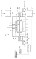
- the vacuum processing apparatus 1 includes a vacuum vessel 2, a substrate holder 3, a substrate support member 10a, and a moving mechanism that attracts the substrate 15 to the substrate holder 3.
- the vacuum vessel 2 is a vessel that can be evacuated.
- the substrate holder 3 is provided in the vacuum vessel 2, has a substrate suction surface 5 a that faces vertically downward, and has an electrostatic suction mechanism that electrostatically attracts the substrate 15. I have.
- the substrate support member 10a is provided in the vacuum vessel 2 and keeps the substrate 15 and the substrate suction surface 5a of the substrate holder 3 parallel to each other. It is a member that supports the substrate 15 in an adsorbable posture.
- the moving mechanism moves at least one of the substrate 15 and the substrate holder 3 supported by the substrate support member 10a, and brings the substrate 15 into the substrate holder 3 by bringing them into contact with each other. It functions as a means for adsorption.
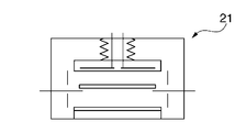
- FIG. 1 is a schematic diagram showing the configuration of the first embodiment in the vacuum processing apparatus 1 of the present invention.
- a plurality of chambers vacuum containers that are connected to an evacuation system (not shown) and can be evacuated are provided as a transfer chamber 22 that can be evacuated. It is configured to be connected through a gate valve 23.
- the chamber connected to the transfer chamber 22 includes, for example, a load lock chamber 24 that introduces the substrate 15 into the vacuum processing apparatus 1, a substrate processing chamber 21 that vacuum-processes the substrate 15, and an unloader that collects the processed substrate 15.
- the vacuum processing apparatus 1 of FIG. 1 includes four substrate processing chambers 21, one load lock chamber 24, and one unload lock chamber 25, but the embodiment of the present invention is limited to this. It is not a thing.
- the transfer chamber 22 is provided with a transfer robot 14 which is a substrate transfer mechanism, and can transfer the substrate 15 to each chamber.
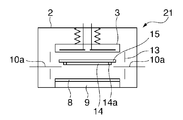
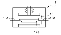
- FIG. 2 is a schematic view showing a configuration centering on the substrate processing chamber 21 provided in the vacuum processing apparatus 1 of FIG.
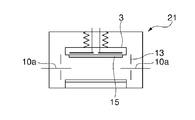
- the substrate holder 3 has an electrostatic chuck holder 5.
- the vertically lower surface (substrate suction surface 5 a) of the electrostatic chuck holder 5 is parallel to the surface of the substrate 15.
- the electrostatic chuck holder 5 is made of a dielectric material, and a plurality of (two in this embodiment) electrostatic chuck electrodes 6 and 7 are provided inside.
- each electrostatic adsorption electrode 6 and 7 is connected to an electrostatic adsorption DC power supply (ESC DC power supply) 12, and a voltage is applied to each electrostatic adsorption electrode 6 and 7 so as to produce a voltage difference.
- ESC DC power supply electrostatic adsorption DC power supply
- a controller for controlling the DC power supply 12 for ESC is provided.
- the substrate holder 3 is connected to a moving mechanism (not shown) that is driven up and down and is movable up and down.
- the target 8 is located in the lower part inside the vacuum vessel 2 and is arranged in a state facing the electrostatic chuck holder 5 of the upper substrate holder 3 in a parallel position.
- a DC power supply 11 is connected to the target 8, and a predetermined voltage is applied from the DC power supply 11 to the target 8. That is, the target 8 forms a cathode part.
- the power source connected to the target 8 is not limited to the DC power source, and may be an RF power source having a frequency of 13.56 MHz, for example.
- a magnet unit 9 is arranged on the back of the target 8.
- a specific magnetic field distribution is formed on the surface of the target 8 by the magnet unit 9.
- the magnet used for the magnet unit 9 is an electromagnet, a permanent magnet, or the like. A combination of a plurality of these magnets may be used.
- the necessary target 8 is held at a predetermined voltage by the DC power source 12 and the magnet unit 9, and a predetermined magnetic field distribution is formed on the surface of the target 8. Thereby, it can discharge by low pressure and can perform sputtering.
- a shield 13 is provided inside the substrate processing chamber 21.
- the shield 13 is provided to prevent the film from adhering to the inner wall of the substrate processing chamber 21 during film formation by sputtering on the substrate 15 placed on the substrate holder 3.
- the shield 13 has a shape (for example, a substantially cylindrical shape) surrounding the discharge space between the substrate holder 3 and the target 8. (Shown) is formed.
- the substrate support mechanism 10 includes a substrate support member 10a on which a substrate 15 can be placed, and has a structure in which the substrate 15 is supported in a posture capable of adsorbing to the substrate adsorption surface 5a. Specifically, as shown in FIG. 2, the substrate 15 can be supported in parallel to the substrate suction surface 5a. In the present embodiment, the substrate 15 is horizontal when the substrate 15 is placed.
- the substrate support mechanism 10 includes a drive unit 10b such as an air cylinder (not shown) provided outside the substrate processing chamber 21, and the drive unit 10b can move the substrate support member 10a to the outside of the shield 13. It has a configuration.
- a guide member 10e is fixed to the substrate processing chamber 21 and guides the substrate support member 10a so as to move horizontally.
- the bellows 10 d maintains the vacuum state of the substrate processing chamber 21.
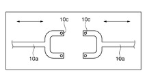
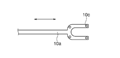
- 3A to 3C are plan views showing the shape of the substrate support member 10a.
- the substrate support member 10a of each substrate support mechanism 10 has a shape capable of contacting the substrate 15 at at least two points apart, and the support height at each contact position.
- a convex contact portion 10c is provided so that the two are aligned.
- the substrate support member 10a is made of a material such as SUS or an aluminum alloy, and is designed to have such rigidity that the tip does not bend due to its own weight.
- the contact part 10c may be formed with SUS, you may use ceramics, such as quartz and an alumina, for example. When quartz or alumina is used, the influence of contamination on the substrate 15 can be suppressed.
- the substrate support member may be only on one side, that is, one, and the contact portion 10c is provided so that the substrate can be supported at least at three points separated by one substrate support member 10a. Is preferred. Further, three or more substrate support members 10a may be arranged. For example, three substrate support members 10a may be arranged as shown in FIG. 3C. In this case, at least one contact portion 10c is provided on each substrate support member 10a.
- the substrate support member 10a is long, even if a design with rigidity is performed, the weight is considerably reduced.
- FIG. 3A and FIG. 3C when the plurality of substrate support members are arranged symmetrically with respect to the center of the substrate, the same amount of the substrate support members 10a is obtained and the substrate 15 is supported horizontally. Can do.
- FIG. 4A to 4G are diagrams for explaining a method for carrying in the substrate 15.
- FIG. The substrate support mechanism 10 shown in FIG. 4A, the movement mechanism (not shown) of the substrate holder 3, and the ESC DC power supply 12 and the power supply 11 shown in FIG. 2 are controlled based on signals from the controller.
- the loading of the substrate 15 is controlled by executing a program in the controller.
- the controller includes a general computer or the like.
- the substrate 15 is placed on the end effector 14 a of the transfer robot 14 and moved vertically below the substrate holder 3.
- the end effector 14a is lowered, and the substrate 15 is placed on the substrate support member 10a as shown in FIG. 4B.
- the substrate holder 3 is vertically lowered from above the substrate 15 and moved to a position immediately before the electrostatic chuck holder 5 provided in the substrate holder 3 and the substrate 15 come into contact with each other as shown in FIG. 4D.
- the substrate holder 3 is further vertically lowered from above the substrate 15 and moved to a position where the electrostatic chuck holder 5 comes into contact with the substrate 15 as shown in FIG. 4E.
- the substrate holder 3 is raised and moved to a predetermined processing position as shown in FIG. 4F.
- the substrate support member 10 a inside the substrate processing chamber 21 is moved outside the shield 13. At this time, as shown in FIG. 4G, the substrate support member 10a is moved to a position where the sputtering material from the target 8 does not adhere to the substrate support member 10a shown in FIG. Evacuation position).
- a predetermined magnetic field distribution is formed on the surface of the target 8 by the magnet unit 9, and a DC negative voltage is supplied from the DC power source 11 to the target 8.
- the discharge is performed at a low pressure, and positive ions in the discharge plasma are drawn into the surface of the target 8 to eject sputtered particles from the target 8.
- the sputtered particles adhere to the substrate 15 and a sputtering film forming process is performed.
- the sputtered particles are scattered in directions other than the substrate 15, but are blocked by the shield 13 and hardly scattered outside the shield 13. Accordingly, almost no sputtered particles are deposited inside the substrate processing chamber 21.
- the discharge pressure may be appropriately adjusted while introducing a gas from a gas introduction system (not shown) during the film formation process from the start of discharge.
- the substrate 15 is unloaded in the reverse order to the introduction of the substrate 15.
- the substrate support member 10a that has been moved to the outside of the shield 13 is moved to the inside of the shield 13 and is stopped vertically below the substrate 15 that is attracted to the electrostatic chuck holder 5 provided in the substrate holder 3 (FIG. 4F). ).
- the substrate holder 3 is vertically lowered, and the substrate 15 adsorbed by the electrostatic adsorption holder 5 is moved to a position where it contacts the substrate support member 10a (FIG. 4E).
- the substrate 15 is moved out of the substrate processing chamber 21 by the end effector 14a (FIG. 4B, A).
- FIG. 5 is a graph showing the effects when the vacuum processing apparatus 1 according to the first embodiment of the present invention is used and when the conventional apparatus is used.
- the horizontal axis indicates the number of substrates processed continuously
- the vertical axis indicates the number of abnormal discharges per substrate observed during the processing of the substrates. It is already known that the number of abnormal discharges has a proportional relationship with the number of foreign substances (particles) that fall on and adhere to the target from above the target.
- abnormal discharge is determined by monitoring voltage and current in a DC power source for discharge.
- the substrate holder 3 may include a temperature adjusting mechanism.
- the temperature adjustment mechanism adjusts the temperature of the substrate suction surface 5a shown in FIG.
- the temperature adjusting mechanism is, for example, a mechanism that circulates a liquid heat transfer medium through a heater built in the substrate holder 3 or the substrate holder 3.
- the heater and the heat transfer medium circulation mechanism may be used in combination in order to increase the temperature controllability of the substrate holder 3.
- the temperature adjustment mechanism when it is necessary to increase the substrate processing temperature, it is preferable to increase the temperature of the substrate holder 3 by the temperature adjustment mechanism and to increase the temperature of the substrate 15 to be processed by the radiant heat from the substrate holder 3.
- the substrate 15 transported from the outside of the substrate processing chamber 21 is at a lower temperature than the temperature of the substrate holder 3.
- the substrate 15 When the substrate 15 is placed on the substrate holder 3 while the temperature of the substrate 15 is lower than the temperature of the substrate holder 3 that has been raised in advance and electrostatic adsorption is performed, the substrate 15 expands as the temperature of the substrate 15 rises. However, since an adsorption force is acting between the substrate holder 3 and the substrate 15 at this time, the surface of the substrate holder 3 and the surface of the substrate 15 are rubbed, and the surface of the substrate holder 3 or the surface of the substrate 15, Or a foreign material (particle) may generate
- the positional relationship between the substrate 15 and the substrate holder 3 is maintained while the substrate 15 is close to the substrate holder 3, and the radiant heat from the substrate holder 3 is maintained. Therefore, it is desirable to raise the temperature of the substrate 15 in advance until it reaches the same temperature as the substrate holder 3.
- FIG. 6 is a flowchart showing the control of the controller in the second embodiment.
- the positional relationship between the substrate holder 3 and the substrate support mechanism 10 is the same as that shown in FIGS. 4A to 4G.
- step S101 the controller operates the temperature adjustment mechanism of the substrate holder 3 to adjust the suction surface with the substrate 15 to a desired temperature.
- step S102 the substrate 15 is placed on the end effector 14a of the transfer robot 14 and moved vertically below the substrate holder 3 (FIG. 4A).
- step S103 the end effector 14a is lowered and the substrate 15 is placed on the substrate support member 10a (FIG. 4B).
- step S104 the end effector 14a is retracted from the substrate processing chamber 21 (FIG. 4C).
- step S105 the substrate holder 3 is vertically lowered from above the substrate 15 and moved to a position just before the electrostatic chuck holder 5 of the substrate holder 3 contacts the substrate 15 as shown in FIG. 4D.
- the substrate 15 is heated using radiant heat from the surface of the electrostatic chuck holder 5. Although the substrate 15 expands as the temperature rises due to this heating, the expansion of the substrate 15 converges as the rise in substrate temperature saturates.
- the predetermined time is, for example, a time until the substrate temperature is saturated after the suction surface 5a is heated to a predetermined temperature by the temperature adjustment mechanism of the substrate holder 3 and the substrate holder 3 is brought close to the substrate 15. Obtained in advance and set this time as a predetermined time.
- step S107 the substrate holder 3 is further lowered vertically from above the substrate 15 to a position where it contacts the substrate 15 where thermal expansion has converged. .
- step S108 a voltage is applied to the electrostatic adsorption electrodes 6 and 7 so as to generate a voltage difference. Thereby, the substrate 15 is attracted to the electrostatic attraction holder 5 provided in the substrate holder 3.
- a temperature sensor such as a thermistor may be provided inside the substrate holder 3 or at the interface between the electrostatic chuck holder 5 and the substrate holder 3.
- the data detected with this temperature sensor may be input into a controller, and the timing which makes the board
- a determination criterion for determining the timing for example, it may be determined whether the temperature change between the electrostatic chuck holder 5 and the substrate 15 has been saturated, or whether the substrate 15 has reached a predetermined saturation temperature. Also good. Further, it may be determined whether the substrate 15 has reached a predetermined temperature, or may be determined based on whether a plurality of temperature sensors are provided and the temperature difference at each location is saturated.
- step S109 the substrate holder 3 is raised and moved to a predetermined processing position as shown in FIG. 4F.
- step 110 the substrate support member 10a is moved to the outside of the shield 13 outside the substrate processing chamber 21, and the substrate support member 10a is moved to a position where the sputtering material from the target 8 does not adhere as shown in FIG. 4G.
- FIG. 4G Retreat and start the film forming process.
- the end effector 14a is also heated. End up.
- the heat is conducted to the robot, and the drive system of the robot is heated. If that happens, the robot will not work or may malfunction. Therefore, when the vacuum processing apparatus 1 according to the embodiment of the present invention is used, the time during which the end effector 14a is positioned under the substrate holder 3 can be shortened, and the end effector 14a can be prevented from being heated. For this reason, the malfunction etc. of the robot mentioned above can be suppressed.
- the substrate 15 is heated with the substrate 15 placed on the end effector 14a, the substrate 15 cannot be transported during that time, resulting in a decrease in throughput in the case of a vacuum processing apparatus having a plurality of chambers. Therefore, when the vacuum processing is performed using the substrate support member 10a as in the vacuum processing apparatus 1 of the present invention, the problem of throughput is solved.
- the application of the present invention is not limited to this. That is, if the processing surface of the substrate is directed vertically downward and the processing is performed with the substrate 15 fixed to the substrate holder by electrostatic adsorption, a physical vapor deposition (PVD) device other than sputtering, a CVD device, an ALD device, a dry device is used. It is suitably applied to an etching apparatus or the like.
- PVD physical vapor deposition
- the present invention is applicable, for example, to the manufacture of the following electronic device.
- powdery deposits are likely to occur on members other than the substrate, and these powdery deposits tend to become particles due to their weak adhesion. Examples include ITO (indium tin oxide) used in LCDs, PZT (lead zirconate titanate) used in piezoelectric elements and ferroelectric memories, etc.
- the face-down type is effective in suppressing the mixing of particles into the surface.
- a face-down type because the melting point of Ga metal is as low as 29.8 ° C.
- the basis of the present invention is a face-down type vacuum processing apparatus that suppresses mixing of particles on a substrate. Therefore, it can be suitably applied to any processing apparatus and electronic device manufacturing having the problem of mixing particles on the same substrate.
- the substrate support mechanism 10 is not limited to horizontally moving the substrate support member 10a.
- the substrate support member 10a moves the substrate support member 10a upward during suction, and retracts the substrate support member 10a downward during vacuum processing.
- the substrate support member 10a may be moved in the horizontal direction and the vertical direction.
- the base portion of the substrate support member 10a may extend to the outside of the vacuum vessel 2.
- the substrate suction surface 5a facing vertically downward has been described, but the gist of the present invention is not limited to this example.
- the substrate 15 is configured to be supported in parallel to the substrate suction surface 5a by the substrate support member 10a, the substrate suction surface 5a may be inclined.
- the substrate holding force force for holding the substrate
- the force (substrate load) required for holding the substrate during the process for example, In the case of a power failure
- the substrate support member 10a is arranged below the substrate holder 3.
- an urging member 30 that continues to urge the substrate support member 10a to the transfer position below the substrate holder 3 when the substrate support member 10a is in the retracted position is provided.
- the urging force of the urging member 30 is configured to move the substrate support member 10a to the transfer position when the operation of the drive unit 10b is stopped due to a power failure or the like.
- the urging member 30 is, for example, a cylinder that moves the substrate support member 10a in the translational direction (from the retracted position to the transfer position or from the transfer position to the retracted position) by the elastic force of an elastic body (spring or fluid). Composed.
- the driving unit 10b of the substrate support member 10a can use this urging force as it is when the substrate support member 10a is driven in the transfer position direction. Further, the driving unit 10b can generate an additional driving force to drive the substrate support member 10b to drive the substrate support member 10a in the direction of the transfer position.
- the substrate support member 10a may be driven by generating a driving force in the opposite direction equal to or greater than the urging force in the retracted position direction.
- the drive unit 10b when configured by an air cylinder or a hydraulic cylinder, it may be a single-action cylinder that generates only a driving force in the retracted position direction, and is driven in both the retracted position direction and the transfer position direction. You may comprise as a double acting cylinder which can generate force.
- the urging member 30 and the drive unit 10b are configured separately, but the urging member 30 and the drive unit 10b may be configured integrally, for example, transfer It can also be configured as a single acting cylinder whose position is a normal position (normal position).
- the moving mechanism 33 of the substrate holder 3 includes a single-acting cylinder whose transfer position is a normal position, and moves the substrate holder 3 up and down based on a command from the controller.
- FIG. 8a of FIG. 8 has shown the state of the vacuum processing apparatus 1 in process.
- this state it is assumed that power supply to the electrostatic adsorption electrodes 6 and 7 is stopped due to, for example, a power failure.
- the substrate 15 is held by the substrate holder 3 for a while due to the residual charge, but eventually loses its holding force and falls due to its own weight.
- the supply of the driving force from the driving source is also stopped, and the substrate support member 10a is driven to the transfer position by the urging force of the urging member 30.
- the driving mechanism 33 of the substrate holder 3 stops supplying driving force, and the substrate holder 3 is lowered to the transfer position by the load of the substrate holder 3.
- the substrate support member 10a can receive it, and the substrate 15 and the target can be prevented from being damaged.
- the substrate holder 3 is also lowered at the same time, the drop distance can be shortened and the substrate can be more reliably prevented from falling.
- the substrate supporting member 10a is moved into the substrate processing chamber 21 when the substrate holding force is lower than the force (substrate load) required to hold the substrate during the process, thereby allowing the substrate to be moved. It can be made to function as a mechanism for preventing the fall of the substrate, and the problem of the fall of the substrate peculiar to the face down can be solved.
- the substrate falls, it is necessary to stop the line and to expose the inside of the substrate processing chamber 21 to the atmosphere in order to replace the target that receives the dropped substrate and to remove fragments of the substrate. And the damage required for recovery will increase.
- the vacuum processing apparatus according to the third embodiment may be further provided with a fall prevention sensor for detecting a substrate adsorption failure to detect that the substrate holding force is lower than the substrate load.
- a fall prevention sensor for detecting a substrate adsorption failure to detect that the substrate holding force is lower than the substrate load.
- the fall prevention operation of the vacuum processing apparatus according to the fourth embodiment provided with the fall prevention sensor will be described.
- the biasing member 30 of the third embodiment causes the substrate support member 10a to be placed at the fall prevention position (transfer position).
- the controller of the apparatus executes the following processing. First, when a power failure occurs, the output of the working fluid is automatically stopped (S901).
- the substrate support member 10a is driven by the urging member 30, and the substrate support member 10a is moved below the substrate holder 3 (S902).
- the substrate holder 3 is lowered by its own weight, and the substrate support member 10a receives the substrate 15 (S903).
- the controller of the vacuum processing apparatus performs the following processing. First, the controller detects that a suction failure has occurred based on the current value (S904). Then, the controller drives the substrate support member (S905), arranges it below the substrate holder 3, and receives the substrate 15 (S906). Thereby, the fall of the board
- the fall prevention sensor for example, when a gas for heat transfer is caused to flow on the back side of the substrate 15 adsorbed to the electrostatic chuck holder 5, a pressure sensor for measuring the pressure in the space on the back side of the substrate 15. And a sensor that detects that the pressure is equal to or lower than a predetermined value. That is, when the substrate 15 is not attracted to the electrostatic attraction holder 5, gas leaks from the space on the back surface side, and the predetermined pressure cannot be maintained. Therefore, the suction failure of the substrate 15 can be detected by detecting that the pressure sensor does not reach the predetermined pressure.
- the controller of the fourth embodiment determines that the pressure falls below a predetermined threshold (predetermined pressure) based on the output from the pressure sensor, the pressure sensor normally attracts the substrate 15 to the electrostatic chuck holder 5. It judges that it is not carried out, and the command which arrange
- a predetermined threshold predetermined pressure
Abstract
Priority Applications (5)
| Application Number | Priority Date | Filing Date | Title |
|---|---|---|---|
| JP2010517738A JP4603099B2 (ja) | 2008-06-20 | 2009-06-19 | 真空処理装置、真空処理方法及び電子デバイスの製造方法 |
| EP09766450A EP2290678A1 (fr) | 2008-06-20 | 2009-06-19 | Appareil de traitement a vide, procede de traitement a vide, et procede de fabrication d' un dispositif electronique |
| CN200980119910.9A CN102047406B (zh) | 2008-06-20 | 2009-06-19 | 真空处理设备、真空处理方法和电子装置制造方法 |
| US12/952,814 US20110064880A1 (en) | 2008-06-20 | 2010-11-23 | Vacuum processing apparatus, vacuum processing method, and electronic device manufacturing method |
| US13/648,669 US8709218B2 (en) | 2008-06-20 | 2012-10-10 | Vacuum processing apparatus, vacuum processing method, and electronic device manufacturing method |
Applications Claiming Priority (2)
| Application Number | Priority Date | Filing Date | Title |
|---|---|---|---|
| JP2008161477 | 2008-06-20 | ||
| JP2008-161477 | 2008-06-20 |
Related Child Applications (1)
| Application Number | Title | Priority Date | Filing Date |
|---|---|---|---|
| US12/952,814 Continuation US20110064880A1 (en) | 2008-06-20 | 2010-11-23 | Vacuum processing apparatus, vacuum processing method, and electronic device manufacturing method |
Publications (1)
| Publication Number | Publication Date |
|---|---|
| WO2009154002A1 true WO2009154002A1 (fr) | 2009-12-23 |
Family
ID=41433920
Family Applications (1)
| Application Number | Title | Priority Date | Filing Date |
|---|---|---|---|
| PCT/JP2009/002802 WO2009154002A1 (fr) | 2008-06-20 | 2009-06-19 | Appareil de traitement à vide, procédé de traitement à vide, et procédé de fabrication d’un dispositif électronique |
Country Status (5)
| Country | Link |
|---|---|
| US (2) | US20110064880A1 (fr) |
| EP (1) | EP2290678A1 (fr) |
| JP (1) | JP4603099B2 (fr) |
| CN (1) | CN102047406B (fr) |
| WO (1) | WO2009154002A1 (fr) |
Cited By (2)
| Publication number | Priority date | Publication date | Assignee | Title |
|---|---|---|---|---|
| WO2012090422A1 (fr) * | 2010-12-27 | 2012-07-05 | キヤノンアネルバ株式会社 | Procédé de formation de couches épitaxiales, appareil de pulvérisation cathodique, procédé de fabrication d'un élément électroluminescent à semi-conducteur et dispositif d'éclairage |
| WO2014002465A1 (fr) * | 2012-06-26 | 2014-01-03 | キヤノンアネルバ株式会社 | Procédé de formation d'un film épitaxial, dispositif de pulvérisation, procédé permettant de fabriquer un élément électroluminescent semi-conducteur, élément électroluminescent semi-conducteur et dispositif d'éclairage |
Families Citing this family (1)
| Publication number | Priority date | Publication date | Assignee | Title |
|---|---|---|---|---|
| US9929121B2 (en) * | 2015-08-31 | 2018-03-27 | Kulicke And Soffa Industries, Inc. | Bonding machines for bonding semiconductor elements, methods of operating bonding machines, and techniques for improving UPH on such bonding machines |
Citations (11)
| Publication number | Priority date | Publication date | Assignee | Title |
|---|---|---|---|---|
| JPH0354845A (ja) | 1989-07-24 | 1991-03-08 | Fuji Electric Co Ltd | 静電チヤツクからの被処理物の離脱方法 |
| JPH04282848A (ja) * | 1991-03-12 | 1992-10-07 | Fujitsu Ltd | 半導体装置の製造装置 |
| JPH05343507A (ja) | 1992-06-10 | 1993-12-24 | Fujitsu Ltd | 静電吸着方法 |
| JPH07122398A (ja) * | 1993-10-20 | 1995-05-12 | Tokyo Electron Ltd | プラズマ処理装置 |
| JP2001298072A (ja) | 2000-04-14 | 2001-10-26 | Ulvac Japan Ltd | 静電吸着装置及びこれを用いた真空処理装置 |
| JP2003241202A (ja) * | 2002-02-20 | 2003-08-27 | Lg Phillips Lcd Co Ltd | 液晶表示素子用貼り合わせ装置 |
| JP2003255297A (ja) * | 2002-02-22 | 2003-09-10 | Lg Phillips Lcd Co Ltd | 液晶表示素子用真空貼り合わせ装置及びその駆動方法 |
| JP2003255356A (ja) * | 2002-03-05 | 2003-09-10 | Lg Phillips Lcd Co Ltd | 液晶表示素子用貼り合わせ装置 |
| JP2004102215A (ja) * | 2002-07-19 | 2004-04-02 | Hitachi Industries Co Ltd | 基板組立装置 |
| JP2006156905A (ja) * | 2004-12-01 | 2006-06-15 | Nikon Corp | 基板脱落防止装置および露光装置 |
| JP2008161477A (ja) | 2006-12-28 | 2008-07-17 | Sophia Co Ltd | 遊技機 |
Family Cites Families (6)
| Publication number | Priority date | Publication date | Assignee | Title |
|---|---|---|---|---|
| JPS6132504A (ja) | 1984-07-25 | 1986-02-15 | Sumitomo Metal Mining Co Ltd | 垂直磁化磁性薄膜 |
| JPH0688221A (ja) * | 1992-09-07 | 1994-03-29 | Fuji Electric Co Ltd | スパッタリング装置 |
| US5571366A (en) * | 1993-10-20 | 1996-11-05 | Tokyo Electron Limited | Plasma processing apparatus |
| JPH0860355A (ja) * | 1994-08-23 | 1996-03-05 | Tel Varian Ltd | 処理装置 |
| US5820329A (en) * | 1997-04-10 | 1998-10-13 | Tokyo Electron Limited | Vacuum processing apparatus with low particle generating wafer clamp |
| JP4282848B2 (ja) * | 1999-06-04 | 2009-06-24 | 旭化成ケミカルズ株式会社 | 無機粒子分散組成物 |
-
2009
- 2009-06-19 EP EP09766450A patent/EP2290678A1/fr not_active Withdrawn
- 2009-06-19 CN CN200980119910.9A patent/CN102047406B/zh active Active
- 2009-06-19 WO PCT/JP2009/002802 patent/WO2009154002A1/fr active Application Filing
- 2009-06-19 JP JP2010517738A patent/JP4603099B2/ja active Active
-
2010
- 2010-11-23 US US12/952,814 patent/US20110064880A1/en not_active Abandoned
-
2012
- 2012-10-10 US US13/648,669 patent/US8709218B2/en active Active
Patent Citations (11)
| Publication number | Priority date | Publication date | Assignee | Title |
|---|---|---|---|---|
| JPH0354845A (ja) | 1989-07-24 | 1991-03-08 | Fuji Electric Co Ltd | 静電チヤツクからの被処理物の離脱方法 |
| JPH04282848A (ja) * | 1991-03-12 | 1992-10-07 | Fujitsu Ltd | 半導体装置の製造装置 |
| JPH05343507A (ja) | 1992-06-10 | 1993-12-24 | Fujitsu Ltd | 静電吸着方法 |
| JPH07122398A (ja) * | 1993-10-20 | 1995-05-12 | Tokyo Electron Ltd | プラズマ処理装置 |
| JP2001298072A (ja) | 2000-04-14 | 2001-10-26 | Ulvac Japan Ltd | 静電吸着装置及びこれを用いた真空処理装置 |
| JP2003241202A (ja) * | 2002-02-20 | 2003-08-27 | Lg Phillips Lcd Co Ltd | 液晶表示素子用貼り合わせ装置 |
| JP2003255297A (ja) * | 2002-02-22 | 2003-09-10 | Lg Phillips Lcd Co Ltd | 液晶表示素子用真空貼り合わせ装置及びその駆動方法 |
| JP2003255356A (ja) * | 2002-03-05 | 2003-09-10 | Lg Phillips Lcd Co Ltd | 液晶表示素子用貼り合わせ装置 |
| JP2004102215A (ja) * | 2002-07-19 | 2004-04-02 | Hitachi Industries Co Ltd | 基板組立装置 |
| JP2006156905A (ja) * | 2004-12-01 | 2006-06-15 | Nikon Corp | 基板脱落防止装置および露光装置 |
| JP2008161477A (ja) | 2006-12-28 | 2008-07-17 | Sophia Co Ltd | 遊技機 |
Cited By (7)
| Publication number | Priority date | Publication date | Assignee | Title |
|---|---|---|---|---|
| WO2012090422A1 (fr) * | 2010-12-27 | 2012-07-05 | キヤノンアネルバ株式会社 | Procédé de formation de couches épitaxiales, appareil de pulvérisation cathodique, procédé de fabrication d'un élément électroluminescent à semi-conducteur et dispositif d'éclairage |
| CN103329248A (zh) * | 2010-12-27 | 2013-09-25 | 佳能安内华股份有限公司 | 外延膜形成方法、溅射设备、半导体发光元件的制造方法、半导体发光元件和照明装置 |
| JP5576507B2 (ja) * | 2010-12-27 | 2014-08-20 | キヤノンアネルバ株式会社 | エピタキシャル膜形成方法、スパッタリング装置、半導体発光素子の製造方法、半導体発光素子、および照明装置 |
| US10844470B2 (en) | 2010-12-27 | 2020-11-24 | Canon Anelva Corporation | Epitaxial film forming method, sputtering apparatus, manufacturing method of semiconductor light-emitting element, semiconductor light-emitting element, and illumination device |
| WO2014002465A1 (fr) * | 2012-06-26 | 2014-01-03 | キヤノンアネルバ株式会社 | Procédé de formation d'un film épitaxial, dispositif de pulvérisation, procédé permettant de fabriquer un élément électroluminescent semi-conducteur, élément électroluminescent semi-conducteur et dispositif d'éclairage |
| JP5886426B2 (ja) * | 2012-06-26 | 2016-03-16 | キヤノンアネルバ株式会社 | エピタキシャル膜形成方法、スパッタリング装置、半導体発光素子の製造方法、半導体発光素子、および照明装置 |
| US9379279B2 (en) | 2012-06-26 | 2016-06-28 | Canon Anelva Corporation | Epitaxial film forming method, sputtering apparatus, manufacturing method of semiconductor light-emitting element, semiconductor light-emitting element, and illumination device |
Also Published As
| Publication number | Publication date |
|---|---|
| EP2290678A1 (fr) | 2011-03-02 |
| US20110064880A1 (en) | 2011-03-17 |
| JPWO2009154002A1 (ja) | 2011-11-24 |
| US8709218B2 (en) | 2014-04-29 |
| US20130032468A1 (en) | 2013-02-07 |
| JP4603099B2 (ja) | 2010-12-22 |
| CN102047406B (zh) | 2013-06-05 |
| CN102047406A (zh) | 2011-05-04 |
Similar Documents
| Publication | Publication Date | Title |
|---|---|---|
| KR101731003B1 (ko) | 플라즈마 처리 장치 | |
| JP4133333B2 (ja) | 被処理体の処理方法及びその処理装置 | |
| JP5975755B2 (ja) | プラズマ処理装置およびプラズマ処理方法 | |
| WO2010026955A1 (fr) | Elément de support de substrat, appareil de traitement de substrat et procédé de traitement de substrat | |
| US20070227033A1 (en) | Substrate transferring apparatus, substrate processing apparatus, and substrate processing method | |
| JP2019176031A (ja) | プラズマ処理装置、及び被処理体の搬送方法 | |
| JP7134039B2 (ja) | 基板載置機構、成膜装置、および成膜方法 | |
| JP5031186B2 (ja) | 基板処理方法、基板処理システム及び基板処理プログラム | |
| JP2015076458A (ja) | 真空処理装置 | |
| KR102366901B1 (ko) | 기판 처리 장치 및 탑재대의 제전 방법 | |
| JP4603099B2 (ja) | 真空処理装置、真空処理方法及び電子デバイスの製造方法 | |
| JP4783094B2 (ja) | プラズマ処理用環状部品、プラズマ処理装置、及び外側環状部材 | |
| JP2006269556A (ja) | プラズマ処理装置、及び半導体装置の製造方法 | |
| JP2011202190A (ja) | スパッタリング装置及びスパッタリング方法 | |
| JP2014195009A (ja) | プラズマ処理装置およびプラズマ処理方法 | |
| KR102299883B1 (ko) | 기판 처리 장치 및 방법 | |
| JP5497091B2 (ja) | 基板処理方法 | |
| US10014145B2 (en) | Vacuum exhaust method | |
| JP4039645B2 (ja) | 真空処理装置 | |
| KR20210071840A (ko) | 기판 처리 방법 및 기판 처리 장치 | |
| KR102600534B1 (ko) | 기판 처리 장치 및 기판 처리 방법 | |
| JP5531123B1 (ja) | 接合装置及び接合システム | |
| JP2023130880A (ja) | 基板処理室内に配置される部材を搬送する装置、基板処理システム及び前記部材を搬送する方法 | |
| JPH1116995A (ja) | 静電チャックによる半導体ウエハの吸着・保持方法 | |
| JP2017005177A (ja) | プラズマ処理装置およびプラズマ処理方法 |
Legal Events
| Date | Code | Title | Description |
|---|---|---|---|
| WWE | Wipo information: entry into national phase |
Ref document number: 200980119910.9 Country of ref document: CN |
|
| 121 | Ep: the epo has been informed by wipo that ep was designated in this application |
Ref document number: 09766450 Country of ref document: EP Kind code of ref document: A1 |
|
| DPE1 | Request for preliminary examination filed after expiration of 19th month from priority date (pct application filed from 20040101) | ||
| ENP | Entry into the national phase |
Ref document number: 2010517738 Country of ref document: JP Kind code of ref document: A |
|
| WWE | Wipo information: entry into national phase |
Ref document number: 2009766450 Country of ref document: EP |
|
| NENP | Non-entry into the national phase |
Ref country code: DE |