WO2009151045A1 - 電子機器、携帯電話機、フレキシブルケーブル、光導波路形成体の製造方法 - Google Patents
電子機器、携帯電話機、フレキシブルケーブル、光導波路形成体の製造方法 Download PDFInfo
- Publication number
- WO2009151045A1 WO2009151045A1 PCT/JP2009/060512 JP2009060512W WO2009151045A1 WO 2009151045 A1 WO2009151045 A1 WO 2009151045A1 JP 2009060512 W JP2009060512 W JP 2009060512W WO 2009151045 A1 WO2009151045 A1 WO 2009151045A1
- Authority
- WO
- WIPO (PCT)
- Prior art keywords
- optical waveguide
- core
- layer
- forming body
- waveguide forming
- Prior art date
Links
- 230000003287 optical effect Effects 0.000 title claims abstract description 351
- 238000004519 manufacturing process Methods 0.000 title claims description 45
- 238000000034 method Methods 0.000 title claims description 20
- 230000001413 cellular effect Effects 0.000 title abstract description 8
- 239000010410 layer Substances 0.000 claims description 244
- 239000000463 material Substances 0.000 claims description 168
- 239000012792 core layer Substances 0.000 claims description 126
- 238000005452 bending Methods 0.000 claims description 121
- 238000005253 cladding Methods 0.000 claims description 80
- 229920000642 polymer Polymers 0.000 claims description 71
- JFNLZVQOOSMTJK-KNVOCYPGSA-N norbornene Chemical compound C1[C@@H]2CC[C@H]1C=C2 JFNLZVQOOSMTJK-KNVOCYPGSA-N 0.000 claims description 51
- 239000004020 conductor Substances 0.000 claims description 49
- 230000002093 peripheral effect Effects 0.000 claims description 39
- 238000010521 absorption reaction Methods 0.000 claims description 35
- 230000015572 biosynthetic process Effects 0.000 claims description 35
- 230000008054 signal transmission Effects 0.000 claims description 19
- 239000002966 varnish Substances 0.000 claims description 16
- 239000002253 acid Substances 0.000 claims description 10
- 125000004122 cyclic group Chemical group 0.000 claims description 8
- 230000001678 irradiating effect Effects 0.000 claims description 7
- 229920005672 polyolefin resin Polymers 0.000 claims description 7
- 230000008569 process Effects 0.000 claims description 7
- 239000011342 resin composition Substances 0.000 claims description 7
- 238000010894 electron beam technology Methods 0.000 claims description 6
- 125000003518 norbornenyl group Chemical group C12(C=CC(CC1)C2)* 0.000 claims description 3
- 238000002788 crimping Methods 0.000 claims 1
- 230000005540 biological transmission Effects 0.000 abstract description 21
- 238000012360 testing method Methods 0.000 description 69
- 229920001577 copolymer Polymers 0.000 description 44
- 229920005989 resin Polymers 0.000 description 42
- 239000011347 resin Substances 0.000 description 42
- 239000000178 monomer Substances 0.000 description 35
- 239000011248 coating agent Substances 0.000 description 23
- 238000000576 coating method Methods 0.000 description 23
- 229910052751 metal Inorganic materials 0.000 description 22
- 239000002184 metal Substances 0.000 description 22
- 238000010438 heat treatment Methods 0.000 description 16
- 238000007142 ring opening reaction Methods 0.000 description 13
- 150000001993 dienes Chemical class 0.000 description 12
- 238000005259 measurement Methods 0.000 description 11
- 230000000052 comparative effect Effects 0.000 description 10
- 238000003780 insertion Methods 0.000 description 10
- 230000037431 insertion Effects 0.000 description 10
- 239000000758 substrate Substances 0.000 description 10
- 239000007787 solid Substances 0.000 description 9
- 230000009477 glass transition Effects 0.000 description 8
- 238000006243 chemical reaction Methods 0.000 description 7
- 230000006870 function Effects 0.000 description 7
- QSHDDOUJBYECFT-UHFFFAOYSA-N mercury Chemical compound [Hg] QSHDDOUJBYECFT-UHFFFAOYSA-N 0.000 description 7
- 229910052753 mercury Inorganic materials 0.000 description 7
- 229910001507 metal halide Inorganic materials 0.000 description 7
- 150000005309 metal halides Chemical class 0.000 description 7
- 229920001721 polyimide Polymers 0.000 description 7
- 238000003825 pressing Methods 0.000 description 7
- RYGMFSIKBFXOCR-UHFFFAOYSA-N Copper Chemical compound [Cu] RYGMFSIKBFXOCR-UHFFFAOYSA-N 0.000 description 6
- YMWUJEATGCHHMB-UHFFFAOYSA-N Dichloromethane Chemical compound ClCCl YMWUJEATGCHHMB-UHFFFAOYSA-N 0.000 description 6
- VGGSQFUCUMXWEO-UHFFFAOYSA-N Ethene Chemical compound C=C VGGSQFUCUMXWEO-UHFFFAOYSA-N 0.000 description 6
- 239000005977 Ethylene Substances 0.000 description 6
- UMIVXZPTRXBADB-UHFFFAOYSA-N benzocyclobutene Chemical compound C1=CC=C2CCC2=C1 UMIVXZPTRXBADB-UHFFFAOYSA-N 0.000 description 6
- 239000000835 fiber Substances 0.000 description 6
- -1 hexafluoroantimonate Chemical compound 0.000 description 6
- NFHFRUOZVGFOOS-UHFFFAOYSA-N palladium;triphenylphosphane Chemical compound [Pd].C1=CC=CC=C1P(C=1C=CC=CC=1)C1=CC=CC=C1.C1=CC=CC=C1P(C=1C=CC=CC=1)C1=CC=CC=C1.C1=CC=CC=C1P(C=1C=CC=CC=1)C1=CC=CC=C1.C1=CC=CC=C1P(C=1C=CC=CC=1)C1=CC=CC=C1 NFHFRUOZVGFOOS-UHFFFAOYSA-N 0.000 description 6
- 239000000243 solution Substances 0.000 description 6
- 239000004711 α-olefin Substances 0.000 description 6
- 239000002131 composite material Substances 0.000 description 5
- 239000000470 constituent Substances 0.000 description 5
- 239000011889 copper foil Substances 0.000 description 5
- 238000012545 processing Methods 0.000 description 5
- LWHOMMCIJIJIGV-UHFFFAOYSA-N (1,3-dioxobenzo[de]isoquinolin-2-yl) trifluoromethanesulfonate Chemical compound C1=CC(C(N(OS(=O)(=O)C(F)(F)F)C2=O)=O)=C3C2=CC=CC3=C1 LWHOMMCIJIJIGV-UHFFFAOYSA-N 0.000 description 4
- KMRASZKMNHTING-UHFFFAOYSA-N 4-hexylbicyclo[2.2.1]hept-2-ene Chemical compound C1CC2C=CC1(CCCCCC)C2 KMRASZKMNHTING-UHFFFAOYSA-N 0.000 description 4
- 239000004793 Polystyrene Substances 0.000 description 4
- 239000003963 antioxidant agent Substances 0.000 description 4
- 210000000078 claw Anatomy 0.000 description 4
- 238000004132 cross linking Methods 0.000 description 4
- 230000000694 effects Effects 0.000 description 4
- 239000003822 epoxy resin Substances 0.000 description 4
- 229920000647 polyepoxide Polymers 0.000 description 4
- 229920000139 polyethylene terephthalate Polymers 0.000 description 4
- 239000005020 polyethylene terephthalate Substances 0.000 description 4
- 229920002223 polystyrene Polymers 0.000 description 4
- 239000002904 solvent Substances 0.000 description 4
- LWNGJAHMBMVCJR-UHFFFAOYSA-N (2,3,4,5,6-pentafluorophenoxy)boronic acid Chemical compound OB(O)OC1=C(F)C(F)=C(F)C(F)=C1F LWNGJAHMBMVCJR-UHFFFAOYSA-N 0.000 description 3
- 229920000178 Acrylic resin Polymers 0.000 description 3
- 239000004925 Acrylic resin Substances 0.000 description 3
- 102100033806 Alpha-protein kinase 3 Human genes 0.000 description 3
- 101710082399 Alpha-protein kinase 3 Proteins 0.000 description 3
- 229920002799 BoPET Polymers 0.000 description 3
- 239000004642 Polyimide Substances 0.000 description 3
- 230000009471 action Effects 0.000 description 3
- 230000008859 change Effects 0.000 description 3
- 238000006073 displacement reaction Methods 0.000 description 3
- 238000005227 gel permeation chromatography Methods 0.000 description 3
- 238000005984 hydrogenation reaction Methods 0.000 description 3
- 230000013011 mating Effects 0.000 description 3
- 229920002577 polybenzoxazole Polymers 0.000 description 3
- 238000006116 polymerization reaction Methods 0.000 description 3
- 230000009466 transformation Effects 0.000 description 3
- JZEPSDIWGBJOEH-UHFFFAOYSA-N 4-decylbicyclo[2.2.1]hept-2-ene Chemical compound C1CC2C=CC1(CCCCCCCCCC)C2 JZEPSDIWGBJOEH-UHFFFAOYSA-N 0.000 description 2
- 239000004952 Polyamide Substances 0.000 description 2
- VYPSYNLAJGMNEJ-UHFFFAOYSA-N Silicium dioxide Chemical compound O=[Si]=O VYPSYNLAJGMNEJ-UHFFFAOYSA-N 0.000 description 2
- 239000000956 alloy Substances 0.000 description 2
- 229910045601 alloy Inorganic materials 0.000 description 2
- 229920005603 alternating copolymer Polymers 0.000 description 2
- 150000004645 aluminates Chemical class 0.000 description 2
- 230000003078 antioxidant effect Effects 0.000 description 2
- 229920001400 block copolymer Polymers 0.000 description 2
- 150000001642 boronic acid derivatives Chemical class 0.000 description 2
- 238000004891 communication Methods 0.000 description 2
- 239000003431 cross linking reagent Substances 0.000 description 2
- 230000032798 delamination Effects 0.000 description 2
- LNTHITQWFMADLM-UHFFFAOYSA-N gallic acid Chemical compound OC(=O)C1=CC(O)=C(O)C(O)=C1 LNTHITQWFMADLM-UHFFFAOYSA-N 0.000 description 2
- LNEPOXFFQSENCJ-UHFFFAOYSA-N haloperidol Chemical compound C1CC(O)(C=2C=CC(Cl)=CC=2)CCN1CCCC(=O)C1=CC=C(F)C=C1 LNEPOXFFQSENCJ-UHFFFAOYSA-N 0.000 description 2
- 229920001519 homopolymer Polymers 0.000 description 2
- 238000009413 insulation Methods 0.000 description 2
- AUHZEENZYGFFBQ-UHFFFAOYSA-N mesitylene Substances CC1=CC(C)=CC(C)=C1 AUHZEENZYGFFBQ-UHFFFAOYSA-N 0.000 description 2
- 125000001827 mesitylenyl group Chemical group [H]C1=C(C(*)=C(C([H])=C1C([H])([H])[H])C([H])([H])[H])C([H])([H])[H] 0.000 description 2
- 125000005395 methacrylic acid group Chemical group 0.000 description 2
- 239000000203 mixture Substances 0.000 description 2
- 150000002848 norbornenes Chemical class 0.000 description 2
- JRZJOMJEPLMPRA-UHFFFAOYSA-N olefin Natural products CCCCCCCC=C JRZJOMJEPLMPRA-UHFFFAOYSA-N 0.000 description 2
- 230000005693 optoelectronics Effects 0.000 description 2
- 125000000538 pentafluorophenyl group Chemical group FC1=C(F)C(F)=C(*)C(F)=C1F 0.000 description 2
- 229920002647 polyamide Polymers 0.000 description 2
- 229920000515 polycarbonate Polymers 0.000 description 2
- 239000004417 polycarbonate Substances 0.000 description 2
- 229920002959 polymer blend Polymers 0.000 description 2
- 108010001843 pregnancy-associated glycoprotein 2 Proteins 0.000 description 2
- 238000002360 preparation method Methods 0.000 description 2
- 239000000047 product Substances 0.000 description 2
- 229920005604 random copolymer Polymers 0.000 description 2
- 239000000126 substance Substances 0.000 description 2
- 125000001424 substituent group Chemical group 0.000 description 2
- 150000003613 toluenes Chemical class 0.000 description 2
- XLYOFNOQVPJJNP-UHFFFAOYSA-N water Substances O XLYOFNOQVPJJNP-UHFFFAOYSA-N 0.000 description 2
- OVSKIKFHRZPJSS-UHFFFAOYSA-N 2,4-D Chemical compound OC(=O)COC1=CC=C(Cl)C=C1Cl OVSKIKFHRZPJSS-UHFFFAOYSA-N 0.000 description 1
- LKMJVFRMDSNFRT-UHFFFAOYSA-N 2-(methoxymethyl)oxirane Chemical compound COCC1CO1 LKMJVFRMDSNFRT-UHFFFAOYSA-N 0.000 description 1
- BTBUEUYNUDRHOZ-UHFFFAOYSA-N Borate Chemical compound [O-]B([O-])[O-] BTBUEUYNUDRHOZ-UHFFFAOYSA-N 0.000 description 1
- JJKDFBNRRXFUNI-UHFFFAOYSA-N CO[SiH3].C1(=CC=CC=C1)C(C1=CC=CC=C1)C12C=CC(CC1)C2 Chemical compound CO[SiH3].C1(=CC=CC=C1)C(C1=CC=CC=C1)C12C=CC(CC1)C2 JJKDFBNRRXFUNI-UHFFFAOYSA-N 0.000 description 1
- JKIJEFPNVSHHEI-UHFFFAOYSA-N Phenol, 2,4-bis(1,1-dimethylethyl)-, phosphite (3:1) Chemical compound CC(C)(C)C1=CC(C(C)(C)C)=CC=C1OP(OC=1C(=CC(=CC=1)C(C)(C)C)C(C)(C)C)OC1=CC=C(C(C)(C)C)C=C1C(C)(C)C JKIJEFPNVSHHEI-UHFFFAOYSA-N 0.000 description 1
- 235000012545 Vaccinium macrocarpon Nutrition 0.000 description 1
- 235000002118 Vaccinium oxycoccus Nutrition 0.000 description 1
- 244000291414 Vaccinium oxycoccus Species 0.000 description 1
- 230000005856 abnormality Effects 0.000 description 1
- 238000002835 absorbance Methods 0.000 description 1
- 150000001336 alkenes Chemical class 0.000 description 1
- 125000005370 alkoxysilyl group Chemical group 0.000 description 1
- 238000010923 batch production Methods 0.000 description 1
- 230000008901 benefit Effects 0.000 description 1
- QHIWVLPBUQWDMQ-UHFFFAOYSA-N butyl prop-2-enoate;methyl 2-methylprop-2-enoate;prop-2-enoic acid Chemical compound OC(=O)C=C.COC(=O)C(C)=C.CCCCOC(=O)C=C QHIWVLPBUQWDMQ-UHFFFAOYSA-N 0.000 description 1
- 238000010538 cationic polymerization reaction Methods 0.000 description 1
- 150000001768 cations Chemical class 0.000 description 1
- 239000013065 commercial product Substances 0.000 description 1
- 229910052802 copper Inorganic materials 0.000 description 1
- 239000010949 copper Substances 0.000 description 1
- 235000004634 cranberry Nutrition 0.000 description 1
- 238000005520 cutting process Methods 0.000 description 1
- 238000010586 diagram Methods 0.000 description 1
- QPCWAKFDFPYSSW-UHFFFAOYSA-N dimethyl-(2-naphthalen-2-yl-2-oxoethyl)sulfanium Chemical compound C1=CC=CC2=CC(C(=O)C[S+](C)C)=CC=C21 QPCWAKFDFPYSSW-UHFFFAOYSA-N 0.000 description 1
- 238000009826 distribution Methods 0.000 description 1
- 238000005516 engineering process Methods 0.000 description 1
- 125000003700 epoxy group Chemical group 0.000 description 1
- 238000005530 etching Methods 0.000 description 1
- 239000011521 glass Substances 0.000 description 1
- 230000001771 impaired effect Effects 0.000 description 1
- 230000006872 improvement Effects 0.000 description 1
- 239000002648 laminated material Substances 0.000 description 1
- 230000031700 light absorption Effects 0.000 description 1
- 238000003754 machining Methods 0.000 description 1
- 230000007246 mechanism Effects 0.000 description 1
- SSDSCDGVMJFTEQ-UHFFFAOYSA-N octadecyl 3-(3,5-ditert-butyl-4-hydroxyphenyl)propanoate Chemical compound CCCCCCCCCCCCCCCCCCOC(=O)CCC1=CC(C(C)(C)C)=C(O)C(C(C)(C)C)=C1 SSDSCDGVMJFTEQ-UHFFFAOYSA-N 0.000 description 1
- 238000000059 patterning Methods 0.000 description 1
- 239000009719 polyimide resin Substances 0.000 description 1
- 108010001861 pregnancy-associated glycoprotein 1 Proteins 0.000 description 1
- 230000005855 radiation Effects 0.000 description 1
- 239000002994 raw material Substances 0.000 description 1
- 230000009467 reduction Effects 0.000 description 1
- 230000003252 repetitive effect Effects 0.000 description 1
- 239000000377 silicon dioxide Substances 0.000 description 1
- 239000002356 single layer Substances 0.000 description 1
- 239000011343 solid material Substances 0.000 description 1
- 230000003595 spectral effect Effects 0.000 description 1
- 239000010935 stainless steel Substances 0.000 description 1
- 229910001220 stainless steel Inorganic materials 0.000 description 1
- 238000005728 strengthening Methods 0.000 description 1
- 230000001629 suppression Effects 0.000 description 1
- 229920003002 synthetic resin Polymers 0.000 description 1
- 239000000057 synthetic resin Substances 0.000 description 1
- ZMOJTPABCOWEOS-UHFFFAOYSA-N tris(4-tert-butylphenyl)sulfanium Chemical compound C1=CC(C(C)(C)C)=CC=C1[S+](C=1C=CC(=CC=1)C(C)(C)C)C1=CC=C(C(C)(C)C)C=C1 ZMOJTPABCOWEOS-UHFFFAOYSA-N 0.000 description 1
- 238000004804 winding Methods 0.000 description 1
Images


Classifications
-
- G—PHYSICS
- G02—OPTICS
- G02B—OPTICAL ELEMENTS, SYSTEMS OR APPARATUS
- G02B6/00—Light guides; Structural details of arrangements comprising light guides and other optical elements, e.g. couplings
- G02B6/24—Coupling light guides
- G02B6/42—Coupling light guides with opto-electronic elements
- G02B6/43—Arrangements comprising a plurality of opto-electronic elements and associated optical interconnections
-
- H—ELECTRICITY
- H05—ELECTRIC TECHNIQUES NOT OTHERWISE PROVIDED FOR
- H05K—PRINTED CIRCUITS; CASINGS OR CONSTRUCTIONAL DETAILS OF ELECTRIC APPARATUS; MANUFACTURE OF ASSEMBLAGES OF ELECTRICAL COMPONENTS
- H05K1/00—Printed circuits
- H05K1/02—Details
- H05K1/0274—Optical details, e.g. printed circuits comprising integral optical means
-
- G—PHYSICS
- G02—OPTICS
- G02B—OPTICAL ELEMENTS, SYSTEMS OR APPARATUS
- G02B6/00—Light guides; Structural details of arrangements comprising light guides and other optical elements, e.g. couplings
- G02B6/10—Light guides; Structural details of arrangements comprising light guides and other optical elements, e.g. couplings of the optical waveguide type
- G02B6/14—Mode converters
-
- G—PHYSICS
- G02—OPTICS
- G02B—OPTICAL ELEMENTS, SYSTEMS OR APPARATUS
- G02B6/00—Light guides; Structural details of arrangements comprising light guides and other optical elements, e.g. couplings
- G02B6/24—Coupling light guides
- G02B6/42—Coupling light guides with opto-electronic elements
- G02B6/4201—Packages, e.g. shape, construction, internal or external details
- G02B6/4204—Packages, e.g. shape, construction, internal or external details the coupling comprising intermediate optical elements, e.g. lenses, holograms
- G02B6/4214—Packages, e.g. shape, construction, internal or external details the coupling comprising intermediate optical elements, e.g. lenses, holograms the intermediate optical element having redirecting reflective means, e.g. mirrors, prisms for deflecting the radiation from horizontal to down- or upward direction toward a device
-
- G—PHYSICS
- G02—OPTICS
- G02B—OPTICAL ELEMENTS, SYSTEMS OR APPARATUS
- G02B6/00—Light guides; Structural details of arrangements comprising light guides and other optical elements, e.g. couplings
- G02B6/24—Coupling light guides
- G02B6/42—Coupling light guides with opto-electronic elements
- G02B6/4201—Packages, e.g. shape, construction, internal or external details
- G02B6/4246—Bidirectionally operating package structures
-
- H—ELECTRICITY
- H01—ELECTRIC ELEMENTS
- H01R—ELECTRICALLY-CONDUCTIVE CONNECTIONS; STRUCTURAL ASSOCIATIONS OF A PLURALITY OF MUTUALLY-INSULATED ELECTRICAL CONNECTING ELEMENTS; COUPLING DEVICES; CURRENT COLLECTORS
- H01R2201/00—Connectors or connections adapted for particular applications
- H01R2201/16—Connectors or connections adapted for particular applications for telephony
-
- H—ELECTRICITY
- H01—ELECTRIC ELEMENTS
- H01R—ELECTRICALLY-CONDUCTIVE CONNECTIONS; STRUCTURAL ASSOCIATIONS OF A PLURALITY OF MUTUALLY-INSULATED ELECTRICAL CONNECTING ELEMENTS; COUPLING DEVICES; CURRENT COLLECTORS
- H01R35/00—Flexible or turnable line connectors, i.e. the rotation angle being limited
- H01R35/02—Flexible line connectors without frictional contact members
-
- H—ELECTRICITY
- H05—ELECTRIC TECHNIQUES NOT OTHERWISE PROVIDED FOR
- H05K—PRINTED CIRCUITS; CASINGS OR CONSTRUCTIONAL DETAILS OF ELECTRIC APPARATUS; MANUFACTURE OF ASSEMBLAGES OF ELECTRICAL COMPONENTS
- H05K1/00—Printed circuits
- H05K1/02—Details
- H05K1/0277—Bendability or stretchability details
- H05K1/028—Bending or folding regions of flexible printed circuits
-
- H—ELECTRICITY
- H05—ELECTRIC TECHNIQUES NOT OTHERWISE PROVIDED FOR
- H05K—PRINTED CIRCUITS; CASINGS OR CONSTRUCTIONAL DETAILS OF ELECTRIC APPARATUS; MANUFACTURE OF ASSEMBLAGES OF ELECTRICAL COMPONENTS
- H05K1/00—Printed circuits
- H05K1/02—Details
- H05K1/14—Structural association of two or more printed circuits
- H05K1/148—Arrangements of two or more hingeably connected rigid printed circuit boards, i.e. connected by flexible means
-
- H—ELECTRICITY
- H05—ELECTRIC TECHNIQUES NOT OTHERWISE PROVIDED FOR
- H05K—PRINTED CIRCUITS; CASINGS OR CONSTRUCTIONAL DETAILS OF ELECTRIC APPARATUS; MANUFACTURE OF ASSEMBLAGES OF ELECTRICAL COMPONENTS
- H05K2201/00—Indexing scheme relating to printed circuits covered by H05K1/00
- H05K2201/05—Flexible printed circuits [FPCs]
- H05K2201/051—Rolled
Definitions
- the present invention provides a first airframe on which electronic parts are mounted, a second airframe that rotates or slides relative to the first airframe, and a flexible cable that functions as a signal line that connects the first airframe and the second airframe.
- the present invention relates to a method for manufacturing an electronic device, a mobile phone, a flexible cable, and an optical waveguide forming body.
- a cellular phone generally includes a main body provided with operation buttons and a movable side body that rotates or slides relative to the main body, and includes a circuit board and a movable side body provided on the main body.
- the provided circuit board is connected with a flexible signal line (hereinafter also referred to as a flexible cable).
- a flexible signal line hereinafter also referred to as a flexible cable.
- the flexible cable a metal thin wire stored in a flexible resin tube or a flexible wiring board is used.
- the movable side body is rotatably connected to the main body via a hinge part, and the flexible cable passes through the vicinity of the rotation center by the hinge part of the movable side body. In this way, wiring is performed in the machine (for example, Patent Documents 1 and 2).
- optical waveguide substrates hereinafter also referred to simply as optical waveguides
- opto-electric composite substrates in which sheet-shaped optical waveguides are integrated on a circuit board to signal transmission in equipment It is becoming popular.
- the optical waveguide there is a polymer optical waveguide that is easy to manufacture (patterning) and is versatile, in addition to the conventional silica-based optical waveguide, and the latter has been actively developed in recent years.
- the optical waveguide is usually used alone or laminated on a circuit board like the above-described optoelectric composite substrate and handled as a single board-shaped member, and is formed rigid.
- the air brought into contact with the core is overfilled by holes or grooves formed in the cladding.
- Optical waveguides that function as a clad and improve the optical confinement effect are also known (for example, Patent Documents 1, 2, and 3). JP 2005-091469 A JP-A-2005-070324 JP 2003-207661 A
- optical waveguides have not been used for flexible cables, and the introduction of optical waveguides into equipment has not progressed.
- a conventional optical waveguide is usually formed to be rigid for use as a single substrate-shaped member.
- the core portion and the clad portion of the optical waveguide are formed of a solid material. That is, the conventional optical waveguide does not consider use in places where flexibility is required. For this reason, it cannot be used as a flexible cable.
- the flexible cable for signal transmission between the main body and the movable side body that rotates or slides relative to the main body is subjected to bending deformation as the movable side body moves relative to the main body.
- the optical waveguide is formed into a thin sheet (for example, 200 ⁇ m or less), it is possible to make the bending radius very small. However, it is difficult to ensure the bending resistance of the optical waveguide simply by reducing the thickness. Become. Note that the folding resistance refers to mechanical durability for making it difficult to cause bending or the like (for example, bending or breakage of the core portion) that causes an increase in optical loss. The above-mentioned problem has become a large practical impediment when an optical waveguide is used for the flexible cable.
- This invention is made
- the present invention employs the following means in order to solve the above problems.
- a first airframe on which electronic components are mounted a second airframe provided so as to be movable relative to the first airframe, and signal transmission between the first airframe and the second airframe.
- the flexible cable includes a resinous optical waveguide forming body that is flexible and formed in a strip shape or a linear shape, and the second body with respect to the first airframe. A deformed portion that is subjected to bending deformation with relative movement of the airframe, and the optical waveguide forming body is refracted more than the core portion extending along the longitudinal direction of the optical waveguide forming body.
- the clad is inside One or side and a plurality of the core portions are provided, and the air clad built-in portion has the air layer on the outer peripheral side through the core portion when the deformation portion is subjected to bending deformation.
- An electronic device provided with According to a second aspect of the present invention the second aircraft is rotatably connected to the first aircraft via a hinge portion, and the flexible cable extends and is arranged via the hinge portion,
- An electronic apparatus according to a first aspect of the present invention has the deformation portion in the vicinity of the hinge portion between one body and the second body.
- the second body is provided so as to slide with respect to the first body along a guide rail provided in the first body, and the first body and the second body.
- the electronic device according to the first aspect of the present invention has the deformation portion to which bending deformation is given as the second airframe slides relative to the first airframe.
- the air clad built-in portion of the optical waveguide forming body has a position on the inner peripheral side and a position on the outer peripheral side via the core portion when the deformation portion is subjected to bending deformation.
- the electronic device according to the first aspect of the present invention is provided with the air layer.
- the flexible cable includes the optical waveguide forming body, and a strip-shaped flexible wiring board that extends along the optical waveguide forming body and is joined to the optical waveguide forming body.
- the electronic device according to the first aspect of the present invention, wherein the optical waveguide forming body is bent and deformed in a direction toward the inner peripheral side of the flexible wiring board.
- the flexible wiring board includes an electrically insulating base film and a conductor layer provided on one surface of the base film, and the conductor layer is interposed between the optical waveguide and the optical waveguide.
- An electronic device according to a fifth aspect of the present invention is provided that is bonded to the optical waveguide forming body in a direction opposite to the forming body.
- the first body and the second body are respectively a light emitting element or a light receiving element that is optically connected to the optical waveguide forming body of the flexible cable, and the flexible wiring board of the flexible cable.
- a cable connecting portion including an electrode portion electrically connected to a conductor circuit formed by the conductor layer, and the flexible cable has an optical connection between the optical waveguide forming body and the optical element at both ends; and
- An electronic apparatus includes a connector for realizing electrical connection between a conductor circuit formed by the conductor layer of the flexible wiring board and the electrode portion.
- the optical waveguide forming body includes a core layer in which one or a plurality of the core portions are formed between a pair of cladding layers having a refractive index lower than that of the core portion, The portion other than the core portion of the core layer and the cladding layer are the cladding portion having a refractive index lower than that of the core portion, and the optical waveguide forming body is disposed on both sides of the cladding layer via the core layer.
- the air clad built-in portion in which the air layer is secured by a groove formed along the longitudinal direction of the core portion at a position facing one or both of the core portions of the first invention. Provide electronic equipment.
- the core layer of the optical waveguide forming body is composed of a resin composition whose main index is a cyclic olefin resin, and whose refractive index changes when irradiated or heated with an active energy ray or an electron beam.
- An electronic apparatus according to a ninth aspect of the present invention is provided in which the core portion is formed by partially irradiating the layered body for a core layer with the active energy ray or the electron beam.
- An eleventh invention provides a mobile phone which is an electronic device according to any one of the first to tenth inventions.
- an electronic apparatus including a first airframe on which electronic components are mounted and a second airframe that rotates or slides relative to the first airframe.
- the first airframe and the second airframe A flexible cable provided as a signal line for connecting a resin, comprising a resinous optical waveguide forming body having flexibility and formed in a strip shape or a linear shape, and the optical waveguide forming body includes a pair of cladding layers
- the core layer of the optical waveguide forming body between which the core part is formed or a plurality of the core parts are formed, the part other than the core part of the core layer, and the cladding layer have a refractive index lower than that of the core part.
- the thirteenth invention further provides a flexible cable according to the twelfth invention, further comprising a strip-shaped flexible wiring board extending along the optical waveguide forming body and joined to the optical waveguide forming body.
- the flexible wiring board includes an electrically insulating base film and a conductor layer provided on one surface of the base film, and the conductor layer is interposed between the optical waveguide and the optical waveguide.
- a flexible cable according to a thirteenth aspect of the present invention is provided that is joined to the optical waveguide forming body in a direction opposite to the forming body.
- an optical connection between the optical element provided in the electronic device and the optical waveguide forming body, and an electronic circuit provided in the electronic device and the conductive layer of the flexible wiring board are formed.
- a flexible cable according to a thirteenth aspect of the present invention is provided which has connectors for realizing electrical connection with a conductor circuit to be provided at both ends.
- an optical connection between an optical element provided in the electronic device and the optical waveguide forming body, and an electronic circuit provided in the electronic device and the conductive layer of the flexible wiring board are formed.
- a flexible cable according to a fourteenth aspect of the present invention which includes connectors for realizing electrical connection with a conductor circuit to be provided at both ends.
- a seventeenth aspect of the invention is a method for producing a resinous optical waveguide forming body having flexibility and formed in a strip shape or a linear shape, and a core layer having one or more core portions between a pair of clad layers And a portion of the core layer other than the core portion and a clad portion having a refractive index lower than that of the core portion, and a portion facing the core portion of the pair of clad layers in the longitudinal center portion thereof
- the core layer forming film material is heated to produce a difference in refractive index between the irradiation region of the ultraviolet light and the non-irradiation region not irradiated with the ultraviolet light in the core layer forming material.
- a film material for forming a clad layer which is formed into a film by a material containing a second photoacid generator that is activated by irradiation with ultraviolet light to generate an acid, and the groove is formed on one surface thereof; of Thermocompression bonding to a surface to obtain a material laminate comprising the core layer and the clad layer forming film material, and the material laminate includes an absorption maximum wavelength of the second photoacid generator; Clading step of obtaining the clad layer by irradiating ultraviolet light having a wavelength not including the absorption maximum wavelength of the first photoacid generator, and then heating the material laminate to cure the clad layer forming film material.
- the manufacturing method of the optical waveguide formation body which comprises this is provided.
- thermocompression bonding step in the thermocompression bonding step, a varnish containing a cladding layer forming material is applied to a flexible wiring substrate to form a cladding layer forming film material, and the cladding layer prepared separately from the cladding layer forming film material
- a manufacturing method of an optical waveguide forming body according to a seventeenth aspect of the present invention is provided, wherein a forming film material and the core layer are superposed and thermocompression bonded to each other.
- the nineteenth invention provides the method for producing an optical waveguide forming body of the seventeenth invention, wherein the polymer of the core layer forming film material and / or the polymer of the cladding layer forming film material is a norbornene-based polymer.
- the polymer for the core layer forming film material and / or the polymer for the cladding layer forming film material is a norbornene-based polymer.
- a twenty-first aspect of the invention provides a flexible cable according to the twelfth aspect of the invention, wherein the flexible cable includes the optical waveguide forming body manufactured by the optical waveguide forming body manufacturing method of the seventeenth aspect of the invention.
- a twenty-second invention provides an electronic device according to the first invention, wherein the flexible cable is the flexible cable of the twenty-first invention.
- a twenty-third invention is a resin-made optical waveguide forming body having flexibility and formed in a strip shape or a linear shape, and a core portion extending along a longitudinal direction of the optical waveguide forming body, and the core A clad part having a lower refractive index than the part, and an air clad built-in part that incorporates an air layer that is in contact with the core part and extends along the longitudinal direction of the core part.
- An optical waveguide provided with a plurality of the core portions, or a plurality of the core portions, and the air clad built-in portion provided with the air layer on the outer peripheral side through the core portion when bending deformation is applied. Formed body.
- the optical waveguide forming body of the flexible cable is bent and deformed at the deforming portion to which the bending deformation is given by the movement (rotation or sliding movement) of the second body relative to the first body. Since the air layer is sometimes provided at a position on the outer peripheral side of the core, sufficient flexibility can be secured and the folding resistance of the core portion can be improved. Therefore, by improving the bending resistance of the optical waveguide forming body against repeated bending, the optical waveguide forming body can be secured with sufficient durability for practical use.
- the flexible cable according to the present invention has a simple configuration. Moreover, if it is the manufacturing method of the optical waveguide formation body which concerns on this invention, the optical waveguide formation body of the said flexible cable can be obtained easily at low cost.
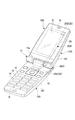
- FIG. 1 is a perspective view showing a mobile phone according to a first embodiment of the present invention. It is a figure which shows the relationship between the circuit board in the 1st body of the mobile phone of FIG. 1, the circuit board in the 2nd body, and the flexible cable (cable with a connector) for signal transmission. It is a figure which shows the relationship between the circuit board in the 1st body in the mobile phone of FIG. 1, the circuit board in the 2nd body, and the flexible cable (cable with a connector) for signal transmission. It is sectional drawing which shows the structure (structure of the cross section along the longitudinal direction of an optical waveguide formation body) of the optical waveguide formation body of the flexible cable of the mobile telephone of FIG.
- FIG. 8 is a diagram illustrating an example of light absorption characteristics of a first photoacid generator and a second photoacid generator used in the production method illustrated in FIG. 7, and the absorption maximum wavelength of the first photoacid generator is in a range of 150 nm to 300 nm. It is a figure which illustrates the case where the thing in this is selected and what has absorption maximum wavelength near 365 nm (I line
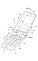
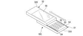
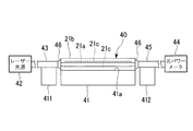
- FIG. 1 is a perspective view showing a mobile phone 10 as an electronic apparatus according to the present invention
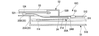
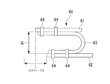
- FIGS. 2A and 2B are circuit boards 111 in a first body 11 and circuit boards 121 in a second body 12 and signals of the mobile phone 10.
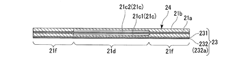
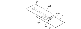
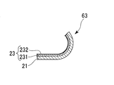
- FIG. 4 is a cross-sectional perspective view showing the structure of the optical waveguide forming body 21
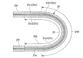
- FIG. 5 is a cross-sectional view showing a state where the deformation portion 21 a of the optical waveguide forming body 21 is bent.
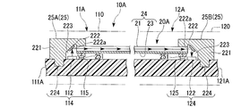
- the mobile phone 10 is a foldable mobile phone, and includes a first body 11 and a first body 11 that is rotatably connected to the first body 11 via a hinge part 13 (pivot part). 2 bodies 12 are provided. Further, the mobile phone 10 includes a flexible strip-shaped optical waveguide formed body 21 made of a synthetic resin, as a flexible cable for signal transmission between the first body 11 and the second body 12, The flexible cable 20 which consists of the connector 22 attached to the longitudinal direction both ends is provided.
- reference numeral 13 a is a pivot that constitutes the hinge portion 13.
- Reference numeral 14 denotes an input operation button, which is provided on the first body 11.
- the first body 11 is also provided with a microphone 15 for transmission, an antenna 16, and a transmission / reception circuit (not shown) connected to the antenna 16.
- the transmission / reception circuit is electrically connected to a circuit of a circuit board 111 (see FIGS. 2A and 2B) housed in the outer case 110 of the first body 11.
- the circuit board 111 is also connected to a switch circuit that is switched by pressing the input operation button 14.
- the second airframe 12 is openable and closable with respect to the first airframe 11 by rotation about the pivot 13a of the hinge portion 13, and is rotated from about 150 to 180 degrees from the closed state with the first airframe 11.
- Reference numeral 17 denotes a display provided in the second machine body 12, and has a display surface exposed on a surface of the second machine body 12 that is closed with respect to the first machine body 11.
- the display 17 is electrically connected to the circuit of the circuit board 121 (see FIGS. 2A and 2B) housed in the exterior case 120 of the second machine body 12.
- the second body 12 is also provided with an audio output unit 18 (speaker). *
- the flexible cable 20 extends from the first body 11 to the second body 12 so that the central portion in the longitudinal direction of the optical waveguide forming body 21 passes through the vicinity of the hinge portion 13. ing.
- One end of the flexible cable 20 in the longitudinal direction is drawn into the exterior case 110 of the first body 11, and the other end in the longitudinal direction is drawn into the exterior case 120 of the second body 12.
- the first body 11 and the second body 21 extend from the hinge portion 13 in parallel with each other.
- the end portion of the first airframe 11 opposite to the hinge portion 13 is hereinafter referred to as a first airframe extension end portion 11a
- the end portion of the second airframe 12 opposite to the hinge portion 13 is referred to as the first airframe extension end portion 11a.
- the optical waveguide forming body 21 of the flexible cable 20 extends the first body extension end portion 11a and the second body extension via the pivot 13a of the hinge portion 13 in a state where the second body 12 is closed to the first body 11.
- the optical waveguide forming body 21 of the flexible cable 20 has openings (not shown) formed in the vicinity of the hinge portion 13 of the outer case 110 of the first body 11 and in the vicinity of the hinge portion 13 of the outer case 120 of the second body 12. ).
- the wiring form of the optical waveguide forming body 21 of the flexible cable 20 in the vicinity of the hinge portion 13 is not limited to the above-described configuration, and for example, the light of the flexible cable 20 is provided between a pair of hinge portions provided apart from each other. A configuration in which the waveguide forming body 21 is passed can also be adopted.
- a feeder line is also disposed between the first body 11 and the second body 12 in addition to the flexible cable 20 for optical signal transmission. Further, a signal line for electric signal transmission may be provided.
- the optical waveguide forming body 21 has a plurality of core portions 21a extending along the longitudinal direction in a clad portion 21b having a refractive index lower than that of the core portion 21a. 3 in FIG. 4).
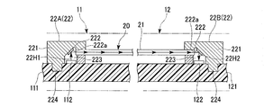
- the optical waveguide forming body 21 is an optical element (light emitting element 112) mounted on the circuit board 111 in the exterior case 110 of the first body 11 by the connectors 22 at both ends in the longitudinal direction.
- the optical element (light receiving element 122) mounted on the circuit board 121 in the exterior case 120 of the second body 12 is optically connected.
- the light signal output from the light emitting element 112 provided in the first machine body 11 receives the light receiving element 122 provided in the second machine body 12 through the optical waveguide forming body 21 of the flexible cable 20.
- one of the connectors 22 at both ends in the longitudinal direction of the flexible cable 20 (longitudinal direction of the optical waveguide forming body 21) is denoted by reference numeral 22A, and the other is denoted by reference numeral 22B.
- the connector 22A is a connector 22 for optically connecting the optical waveguide forming body 21 to the optical element (light emitting element 112) provided on the circuit board 111 of the first body 11, and the connector 22B.
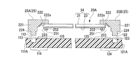
- the connectors 22A and 22B are connected to the optical axis of the optical waveguide corresponding to each core portion 21a of the optical waveguide forming body 21 in the housing 221 attached to the end (longitudinal end) of the optical waveguide forming body 21.
- the mirror 222 which forms the reflective surface 222a inclined by 45 degrees is built in.
- the mirror 222 is disposed in the recess 223 opened on the side surface of the housing 221 and near the end surface of the optical waveguide forming body 21 on the extension of the optical axis at the end surface.
- the formed body 21 is inclined at 45 degrees with respect to the optical axis at the end face.
- a light emitting element 112 is mounted on the circuit board 111 of the first airframe 11, and a connector 22 ⁇ / b> A is provided near the light emitting element 112 as a positioning portion for determining the position of the connector 22 ⁇ / b> A with respect to the light emitting element 112.
- the fitting recess 113 into which the fitting protrusion 224 protruding from the housing 221 is pushed is formed.
- the circuit board 111 is provided with a connector connecting portion including an optical element (light emitting element 112) and a fitting recess 113. As shown in FIG.
- the connector 22A pushes the fitting protrusion 224 protruding from the housing 221 into the fitting recess 113 formed in the circuit board 111 of the first body 11, so that the mirror 222 is
- the optical path 22H1 is installed on the optical axis of the light output from the light emitting element 112 on the circuit board 111 and optically couples the light emitting element 112 and the optical waveguide forming body 21 via the mirror 222. Thereby, the output light from the light emitting element 112 can be incident on the optical waveguide forming body 21 through the mirror 222.
- the light receiving element 122 is mounted on the circuit board 121 of the second machine body 12, and further, in the vicinity of the light emitting element 122, as a positioning portion for determining the position of the connector 22 ⁇ / b> B with respect to the light emitting element 122, A fitting recess 123 into which the fitting protrusion 224 protruding from the housing 221 of the connector 22B is pushed is formed.
- the circuit board 121 is provided with a connector connecting portion including an optical element (light receiving element 122) and a fitting recess 123. As shown in FIG.
- the connector 22B has the same structure as that of the connector 22A, and the fitting protrusion 224 protruding from the housing 221 is formed on the circuit board 121 of the second body 12.
- the mirror 222 is installed on the optical axis of the light received by the light receiving element 122 mounted on the circuit board 121 in the vicinity of the fitting recess 123 by being pushed into the fitting recess 123.
- an optical waveguide forming body 21 are optically coupled to each other through a mirror 222. Thereby, the light transmitted by the optical waveguide forming body 21 can be received by the light receiving element 122.
- the fitting protrusions 224 of the connectors 22A and 22B can be inserted into and removed from the fitting recesses 113 and 123 of the circuit boards 111 and 121.
- This connector is attached to the circuit boards 111 and 121 (connected state) by a pull-out resistance generated when the inner surfaces of the fitting recesses 113 and 123 are pressed against the fitting protrusions 224 press-fitted into the fitting recesses 113 and 123. ), And the mating protrusions 224 fitted in the mating recesses 113 and 123 are pulled out from the mating recesses 113 and 123 by a force exceeding the pull-out resistance, thereby being detached from the circuit boards 111 and 121.
- the structure which enabled it may be sufficient.
- the connector includes the elastic claw and a lever (disengagement lever) that disengages the circuit board by displacing the elastic claw engaged with the circuit board,
- the detachability of the connector can be improved.
- the positioning portion provided on the circuit board is not limited to the fitting recess, and for example, a positioning frame for housing the connector housing, a positioning projection, or the like can be employed.
- the shape of the connector can be changed according to the positioning part on the circuit board side, and the connector can be configured not to have a fitting protrusion.
- one end side of the flexible cable 20 in the longitudinal direction of the optical waveguide forming body 21 is optically connected to the light emitting element 112 of the circuit board 111 of the first machine body 11 by the connector 22 ⁇ / b> A.
- the other end in the direction is optically connected to the light receiving element 122 of the circuit board 121 of the second machine body 12 by the connector 22B. That is, the mobile phone 10 is configured such that the light emitting element 112 of the first machine body 11 and the light receiving element 122 of the second machine body 12 are optically connected via the flexible cable 20.
- the optical waveguide forming body 21 of the flexible cable 20 extends from the first body 11 to the second body 12 through the vicinity of the hinge portion 13 (see FIG. 1), In the vicinity of the hinge portion 13, there is a deformed portion 21 ⁇ / b> H to which a bending deformation is given in accordance with the rotation of the second airframe 12 around the hinge portion 13.
- the optical waveguide forming body 21 has an air clad built-in portion 21d in which an air layer 21c in contact with the core portion 21a is secured at a portion corresponding to the deformed portion 21H.
- the optical waveguide forming body 21 is formed with respect to repeated bending of the deformed portion 21H accompanying the rotation around the hinge portion 13 of the second airframe 12.
- the folding resistance of the body 21 can be improved.
- the optical waveguide forming body 21 is formed in a strip shape having a flat cross section, and a core portion 21 a is linearly formed over the entire length in the longitudinal direction of the optical waveguide forming body 21 at the center in the thickness direction. Further, the core portion 21a is arranged in a row at a plurality of locations (three locations in FIG. 4) in the width direction of the optical waveguide forming body 21.
- the number of core portions 21a is not limited to the three illustrated in FIG. 4, and may be one, two, four, or more (see, for example, FIG. 7F).
- the deformed portion 21H of the optical waveguide forming body 21 is located at the central portion in the longitudinal direction of the optical waveguide forming body 21, and the air clad built-in portion 21d of the optical waveguide forming body 21 is also at the central portion in the longitudinal direction of the optical waveguide forming body 21.
- the air clad built-in portion 21 d of the optical waveguide forming body 21 has the air layer 21 c secured on both sides through the core portion 21 a in the thickness direction of the optical waveguide forming body 21.
- the air layer 21c extends along the longitudinal direction of the core portion 21a.
- grooves 21e extending along the longitudinal direction of the core portion 21a are formed on both sides of the core portion 21a of the cladding portion 21b in the thickness direction of the optical waveguide forming body 21. Is formed.
- the groove 21e is formed so as to be recessed from the core portion 21a side to the clad portion 21b, and an air layer 21c in contact with the core portion 21a is secured in the optical waveguide forming body 21 by the groove 21e. That is, the inside of the groove 21e is an air layer 21c.
- the optical waveguide forming body 21 has a laminated structure including three resin layers 211, 212, and 213.
- the plurality of core portions 21 a of the optical waveguide forming body 21 are formed side by side in the width direction of the optical waveguide forming body 21 on three central resin layers 211 (hereinafter also referred to as core layers).
- the plurality of core portions 21 a are formed at a plurality of locations of the core layer 211 with a space between each other.
- portions of the core layer 211 other than the core portion 21a and resin layers 212 and 213 (hereinafter also referred to as clad layers) provided in a laminated state on both sides of the core layer 211 are refracted more than the core portion 21a.
- the cladding portion 21b having a low rate is configured.
- the groove 21e of the clad portion 21b is formed along the longitudinal direction of the core portion 21a at a location facing the core portion 21a of the clad layers 212 and 213 on both sides via the core layer 211. Therefore, in the air clad built-in portion 21d, the air layer 21c is secured between the clad layers 212 and 213 and the core portion 21a by the groove 21e.
- the manufacturing method of the optical waveguide formation body which consists of three resin layers, and the example of a material are demonstrated later.
- the existence range of the air clad built-in portion 21d in the longitudinal direction of the optical waveguide forming body 21 is wider than the range of the deformed portion 21H.
- the range in which the air clad built-in portion 21 d exists in the longitudinal direction of the optical waveguide forming body 21 is changed to the deformation of the flexible cable 20.
- a range wider than the deformed portion 21H is included so as to include a portion corresponding to the portion 21H and extending on both sides of the range corresponding to the deformed portion 21H in the longitudinal direction of the optical waveguide forming body 21.
- both sides of the air clad built-in portion 21d in the longitudinal direction of the optical waveguide forming body 21 are solid portions 21f (see FIGS. 3 and 5) where the air layer 21c is not formed.
- the optical waveguide forming body 21 of the flexible cable 20 is formed in a straight line shape, and when the second body 12 of the mobile phone 10 is opened about 180 degrees with respect to the first body 11, the deformed portion 21H is almost (or alternatively) At all) no bending deformation is applied.
- the second airframe 12 is closed with respect to the first airframe 11, bending deformation is given to a portion located near the hinge portion 13, that is, the deformation portion 21H. That is, as shown in FIG. 5, in the mobile phone 10, the optical waveguide forming body 21 in the thickness direction is formed on the deformed portion 21 ⁇ / b> H of the optical waveguide forming body 21 with the rotation of the second body 12 with respect to the first body 11.
- a bending deformation (hereinafter also referred to as vertical bending) is applied such that one side is the inner peripheral side and the other side is the outer peripheral side.
- the air layer 21c secured on both sides of the air clad built-in portion 21d of the optical waveguide forming body 21 via the core portion 21a is bent and deformed to the deforming portion 21H of the optical waveguide forming body 21 as shown in FIG.
- One of them hereinafter also referred to as a first air layer.
- Reference numeral 21c1 in FIGS. 3, 4, and 5 is the outer peripheral side of the core portion 21a and the other (hereinafter also referred to as a second air layer). 3, 4, and 5, the reference numeral 21 c 2 is attached to the inner peripheral side of the core portion 21 a.
- the optical waveguide forming body 21 of the flexible cable 20 when the deformation portion 21H is subjected to bending deformation in the air layers 21c1 and 21c2 secured on both sides via the core portion 21a of the optical waveguide forming body 21.
- the first air layer 21c1 located on the outer peripheral side of the core portion 21a effectively contributes to maintaining the optical transmission characteristics of the core portion 21a and improving the folding resistance of the optical waveguide forming body 21.
- the core portion 21a of the cladding portion 21b is applied when bending deformation (vertical bending) is applied.
- the core portion 21a is pressed by the displacement force that the portion located on the outer peripheral side of the bending tends to move toward the inner peripheral side of the bending.
- the first air layer 21c1 causes the first air in the cladding portion 21b.
- a portion located on the opposite side of the core portion 21a via the layer 21c1 (hereinafter also referred to as an outer peripheral side thin portion; reference numeral 21b1) relieves the pressing force applied to the core portion 21a by the displacement force toward the inner peripheral side of the bending or It can be lost.
- the outer peripheral side thin portion 21b1 of the cladding portion 21b does not contact the core portion 21a, and it is possible to prevent the pressing force from being applied to the core portion 21a. Moreover, even if the outer peripheral thin-walled portion 21b1 of the clad portion 21b contacts the core portion 21a, the pressing force applied to the core portion 21a can be suppressed smaller than when a solid structure without the air layer 21c is used. it can. For this reason, even if bending deformation is repeatedly given to the deforming portion 21H, the core portion 21a is unlikely to have a large distortion or breakage that causes an increase in optical loss of the optical waveguide forming body 21.
- the optical waveguide forming body 21 is locally localized. Stress concentration is less likely to occur, and the bending resistance of the optical waveguide forming body 21 is improved.
- the air clad built-in portion 21d having the air layer 21c in contact with both sides of the core portion 21a the inner peripheral side and the outer peripheral side when bending deformation is applied to the deformable portion 21H
- one side of the core portion 21a (deformation)
- the local stress concentration of the body 21 can be made more difficult to occur. Therefore, the above configuration effectively contributes to the improvement of the bending resistance of the optical waveguide forming body 21.
- the clad portion 21b in the thickness direction of the optical waveguide forming body 21 due to the presence of the air layers 21c1 and 21c2 on both sides via the core portion 21a. Since the degree of freedom of deformation of the portions located on both sides can be ensured through the core portion 21a, the cladding portion 21b is hardly damaged by bending deformation. As a result, high mechanical durability can be secured in the air clad built-in portion 21d. This also contributes effectively to improving the bending resistance of the optical waveguide forming body 21 and the core portion 21a.
- the thickness of the clad portion 21b on both sides is reduced via the core portion 21a due to the presence of the air layers 21c1 and 21c2 on both sides via the core portion 21a.
- the air clad built-in portion 21d is more easily bent and deformed than the solid portion 21f, and the bending radius can be reduced.
- the bending radius can be made smaller than that of the solid portion 21f.
- the first air layer 21c1 contributes more effectively than the second air layer 21c2. Therefore, even if the second air layer 21c2 is omitted, the first air layer 21c1 Folding resistance can be easily improved.
- the air layer 21c itself can function as a clad portion (air clad), so that a high light confinement effect can be secured in the optical waveguide forming body 21. Even when bending deformation is given to the deforming portion 21H of the optical waveguide forming body 21, the air layer 21c contributes to the optical confinement effect, and an increase in bending loss can be suppressed.
- FIG. 7A to 7F are views for explaining an example of a method for manufacturing the optical waveguide forming body.
- the optical waveguide forming body 21 ′ shown in FIG. 7F is different from the optical waveguide forming body 21 illustrated in FIG. 4 in that the number of core portions 21a is large.
- the manufacturing method of the optical waveguide forming body described here is applied to the manufacturing of an optical waveguide forming body composed of three resin layers having a structure in which a core layer is provided between two cladding layers.
- the present invention can be similarly applied to the production of the optical waveguide forming body 21 including the three resin layers 211, 212, and 213 exemplified in FIG. The same applies to the materials described later.
- reference numeral 211 ′ denotes a core layer
- 212 ′ and 213 ′ denote cladding layers.
- a core layer forming film material 31 (core layer layered body; a layered body for core layer; see FIG. 7A) obtained by forming a material (core layer forming material) for forming the core layer 211 ′ into a film shape.
- the core layer forming material is mainly composed of a polymer having a main chain and a leaving group branched from the main chain, and further activated by irradiation with ultraviolet light to generate an acid. It contains one photoacid generator.
- Examples of the core layer forming film material 31 include a varnish obtained by dissolving a core layer forming material such as the polymer and the first photoacid generator in a solvent (for example, mesitylene), and a member such as a resin film (for varnish application). A dry coating film applied to a member and dried can be used. This dried coating film is used after being detached from the varnish coating member.
- a solvent for example, mesitylene
- a member for varnish application
- a dry coating film applied to a member and dried can be used. This dried coating film is used after being detached from the varnish coating member.
- the first photoacid generator has an absorption maximum wavelength in the ultraviolet region.
- the polymer of the film material 31 for forming the core layer is separated (cleaved) from the main chain by the action of an acid (preferably proton) released by the activated first photoacid generator upon irradiation with ultraviolet light.
- an acid preferably proton
- the removal of the polymer leaving group proceeds by irradiation with ultraviolet light and subsequent heating.
- the core layer forming film material 31 is cured by heating.
- this optical waveguide forming body manufacturing method an example will be described in which the core layer forming film material 31 employs a material whose refractive index in the irradiated region is lowered by ultraviolet light irradiation and subsequent heating.
- the core layer forming step for example, using a photomask 32 (see FIG. 7A), ultraviolet light having a wavelength that includes the absorption maximum wavelength of the first photoacid generator in a part of the film material 31 for forming the core layer (see FIG. 7A).
- first ultraviolet light having a wavelength that includes the absorption maximum wavelength of the first photoacid generator in a part of the film material 31 for forming the core layer.
- first ultraviolet light After irradiation with the reference numeral 33A) (FIG. 7A), the core layer forming film material 31 is heated to obtain a core layer 211 ′ as shown in FIG. Since the core layer 211 ′ obtained here is in the form of a film, it is also referred to as a core film hereinafter.
- the photomask 32 one having an opening 32a corresponding to the cladding part 21b region of the core layer 211 ′ to be obtained is employed.
- the refractive index of the irradiated region irradiated with the first ultraviolet light 33A is lower than the refractive index of the non-irradiated region not irradiated with the first ultraviolet light 33A.
- a core film 211 ′ which is a single-layer optical waveguide having the irradiation region as the core portion 21a, is obtained. That is, the core part can be patterned by irradiating the film material 31 for forming the core layer with the first ultraviolet light 33 ⁇ / b> A through the photomask 32.
- the film material 31 for forming the core layer a material whose refractive index in the irradiated region is increased by irradiation with the first ultraviolet light 33A may be adopted.
- a photomask having an opening corresponding to the core portion 21a region of the core layer 211 'to be obtained is employed.
- the irradiation region irradiated with ultraviolet light becomes the core portion 21a.
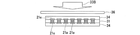
- the clad layer forming film material 34 prepared in advance is thermocompression bonded to both surfaces of the core film 211 ′, and the core film 211 ′ and the clad layer forming film material 34 are A material laminate 35 (FIG. 7D) is obtained (thermocompression bonding step).
- the clad layer forming film material 34 is formed by forming a material for forming the clad layers 212 ′ and 213 ′ (cladding layer forming material) into a film shape, and further, an air layer of the optical waveguide forming body 21 on one side thereof.
- a groove 21e for securing 21c (air clad) is formed.
- the groove 21e has a depth that is 1/3 to 1/2 of the thickness of the clad forming film material 34, and a width (groove width) that is the width of the core portion 21a (the width of the core portion 21a when the core layer is viewed in plan view). In the case of the core portion 21a having a square cross section, it is preferably 2 to 3 times the dimension of one side of the cross section.
- the manufactured optical waveguide is formed. Also in the body, it is preferable that the depth of the groove 21e is 1/3 to 1/2 of the thickness of the cladding layer, and the width is 2 to 3 times the width of the core portion 21a.
- the groove 21e is preferably formed by irradiating a laser (for example, using an excimer laser) on a film obtained by forming a clad layer forming material into a film shape. is there.
- a laser for example, using an excimer laser
- the method for forming the clad layer forming film material 34 having the grooves is not limited to this.
- the clad layer forming material formed into a film shape is subjected to machining such as cutting to form the groove. It is also possible to form a groove or a groove at a desired position by a pattern etching method.
- a clad layer having a groove is formed using a mold member having a protrusion for forming the groove.
- a technique of obtaining the forming film material 34 can also be employed. Further, it is also possible to adopt a technique in which a clad layer forming film material 34 having a groove is obtained by pressing a hot plate having a protrusion for forming a groove on a film formed of the clad layer forming material. is there.
- the cladding layer forming material is mainly composed of a polymer having a polymerizable group, and has an absorption maximum wavelength different from that of the first photoacid generator and is activated by irradiation with ultraviolet light. And a second photoacid generator that generates acid.
- a varnish obtained by dissolving a core layer forming material such as the polymer or the second photoacid generator in a solvent (for example, dehydrated toluene) is used as a member (varnish coating) such as a resin film.
- a dried coating film applied to a member for use and dried can be used. This dried coating film can be used after being detached from the varnish coating member.
- the second photoacid generator also has an absorption maximum wavelength in the ultraviolet region.
- the polymerizable group undergoes a crosslinking reaction by the action of an acid (preferably proton) released by the activated second photoacid generator upon irradiation with ultraviolet light.
- the acid released from the second photoacid generator upon irradiation with ultraviolet rays is for causing a crosslinking reaction in the polymerizable group of the polymer of the film material 34 for forming the cladding layer.
- thermocompression bonding is performed by heating the core film 211 ′ and the clad layer forming film material 34 in a state where the clad layer forming film material 34 is in contact with the core film 211 ′.
- the heating temperature is set to the lower glass transition temperature Tg or higher, whereby the core film 211 ′ and The clad layer forming film material 34 is heated to a temperature equal to or higher than the glass transition temperature, melted, and pressurized to realize thermocompression bonding.
- the entire surface of the material laminate 35 includes the absorption maximum wavelength of the second photoacid generator and absorbs the first photoacid generator.
- the material laminate 35 is heated to cure the clad layer forming film material 34 (cladding step). ).
- the cured clad layer forming film material 34 becomes clad layers 212 ′ and 213 ′ having a refractive index lower than that of the core portion 21 a of the core film 211 ′.
- the crosslinking reaction (cationic polymerization) of the polymerizable group proceeds by ultraviolet light irradiation and subsequent heating (in other words, curing and conversion into the clad layer proceed). Cured) to become a clad layer (clad).
- the adhesion between the core layer 211 ′ and the clad layer forming film material 34 is also improved.
- the heating after the irradiation with the second ultraviolet light ensures a heating time so that the clad layer forming film material 34 is sufficiently clad (crosslinking reaction) and stopped.
- an optical waveguide forming body 21 ′ which is a three-layer optical waveguide having clad layers 212 ′ and 213 ′ on both sides of the core layer 211 ′ is obtained (FIG. 7F).
- the second photoacid generator of the film material for forming a clad layer is activated by irradiation with ultraviolet light having an absorption maximum wavelength different from that of the first photoacid generator to generate an acid.
- the material laminate 35 is irradiated with the second ultraviolet light 33B having a wavelength that includes the absorption maximum wavelength of the second photoacid generator and does not include the absorption maximum wavelength of the first photoacid generator.
- the first photogenerator of the core film 211 ′ is substantially insensitive to the second ultraviolet light 33B, and only the second photoacid generator is substantially sensitive.
- the wavelength cut filter 36 used in the cladding process blocks light with a specified wavelength and a wavelength shorter than the specified wavelength, and transmits only light with a wavelength longer than the specified wavelength.
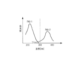
- the absorption maximum wavelength of the first photoacid generator is inevitably shorter than the absorption maximum wavelength of the second photoacid generator.
- the first photoacid generator in FIG. 8, PAG- As 1
- the second photoacid generator PAG-2 in FIG.
- the first photoacid generator having an absorption maximum wavelength of 300 nm or less for example, one having an absorption maximum wavelength in the range of 150 nm to 300 nm
- the second photoacid generator having an absorption maximum wavelength It is preferable to use a film having a wavelength around 365 nm (I line).
- the “absorption maximum wavelength” is, for example, the wavelength (maximum absorption wavelength) when the peak value of absorbance is obtained in the PAG-1 curve and the PAG-2 curve in FIG.
- the entire surface of the material stack 35 of the second ultraviolet light in the cladding step Since the first photogenerator is not substantially sensitive upon irradiation, an acid is generated from the first photoacid generator remaining in the core portion 21a of the core layer 211 ′, and the refractive index generated when the core layer 211 ′ is formed. The difference does not shrink or disappear. That is, the optical waveguide structure of the core layer is not impaired by the entire irradiation of the material layered body with the second ultraviolet light.
- thermocompression bonding can be performed at a temperature near the glass transition temperature Tg of the film material for forming a clad.
- thermocompression bonding process in the subsequent cladding process, even if the heating after the irradiation with the second ultraviolet light is performed by batch processing such as oven heating without applying pressure, the core layer 211 ′ and the cladding layer forming film Adhesion between the material 34 can be sufficiently increased. Since the heating in the cladding process is a batch process, it is possible to process a plurality of material laminates at the same time, which is preferable in terms of improving productivity.
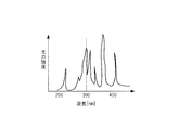
- the irradiation device for the first ultraviolet light and the second ultraviolet light for example, a high-pressure mercury lamp, a metal halide lamp, or the like can be suitably used.
- Irradiation devices such as high-pressure mercury lamps and metal halide lamps have a wide wavelength range of output light, and as shown in FIG. In order to secure sufficient output light intensity, there are provided.
- the material laminate 35 is irradiated with ultraviolet light output from the irradiation device via a wavelength cut filter, the absorption maximum wavelength of the first photoacid generator is determined from the output light of the irradiation device such as a high-pressure mercury lamp or a metal halide lamp. Light can be removed easily and reliably.
- this invention is not limited to the aspect using a wavelength cut filter. There may be a case where the absorption maximum wavelength of the first photoacid generator is longer than the absorption maximum wavelength of the second photoacid generator.
- the molecular structure includes —O— structure, —Si—aryl structure and —O—Si— structure. Those having at least one of the following are preferred. These leaving groups are released relatively easily by the action of cations. Among these, as the leaving group that causes a decrease in the refractive index of the polymer upon leaving, at least one of the —Si-diphenyl structure and —O—Si-diphenyl structure is preferable.
- polymers examples include cyclic olefin resins such as norbornene resins and benzocyclobutene resins, acrylic resins, methacrylic resins, polycarbonates, polystyrenes, epoxy resins, polyamides, polyimides, polybenzoxazoles, and the like.
- cyclic olefin resins such as norbornene resins and benzocyclobutene resins
- One of these or a combination of two or more thereof can be used (for example, polymer alloy, polymer blend (mixture), copolymer, etc.).
- those containing a norbornene-based resin (norbornene-based polymer) as a main component are preferable.
- a norbornene-based polymer as the polymer, a core layer excellent in optical transmission performance
- the norbornene polymer may be either one having a single repeating unit (homopolymer) or one having two or more norbornene repeating units (copolymer).
- Examples of such norbornene-based polymers include (1) addition (co) polymers of norbornene monomers obtained by addition (co) polymerization of norbornene monomers, and (2) norbornene monomers and ethylene or ⁇ -olefins.
- Addition copolymers such as (3) addition copolymers of norbornene type monomers and non-conjugated dienes, and addition copolymers of norbornene type monomers, non-conjugated dienes and other monomers, ( 4) a ring-opening (co) polymer of a norbornene-type monomer, and a resin obtained by hydrogenating the (co) polymer, (5) a ring-opening copolymer of a norbornene-type monomer and ethylene or ⁇ -olefins, and (Co) polymer hydrogenated resin, (6) norbornene-type monomer and non-conjugated diene, or norbornene-type monomer and non-conjugated diene Ring-opening copolymers, and other monomers, and ring-opening polymers such as polymers obtained by hydrogenation of these (co) polymers.
- the polymer examples include a random copolymer, a block copolymer, and an alternating copolymer.
- a norbornene polymer addition polymer in terms of obtaining a core layer having excellent transparency, insulation, flexibility and heat resistance.
- an addition polymer of a norbornene polymer there is an advantage that the refractive index can be adjusted depending on the type of side chain of the addition polymer of the norbornene polymer.
- a homopolymer of diphenylmethylnorbornenemethoxysilane or a copolymer of hexylnorbornene and diphenylmethylnorbornenemethoxysilane can be suitably used.
- Examples of the first photoacid generator include tetrakis (pentafluorophenyl) borate and hexafluoroantimonate, tetrakis (pentafluorophenyl) gallate, aluminate, antimonate, and other borates. , Gallates, carboranes, halocarboranes and the like.
- PHOTOINITIATOR 2074 CAS No.
- TTBPS-TPFPB tris (4-tert-butylphenyl) sulfonium tetrakis (pentapentafluorophenyl) borate
- Examples of the constituent material of the film material 34 for forming the clad layer include cyclic resins such as acrylic resins, methacrylic resins, polycarbonate, polystyrene, epoxy resins, polyamides, polyimides, polybenzoxazoles, benzocyclobutene resins, and norbornene resins.
- cyclic resins such as acrylic resins, methacrylic resins, polycarbonate, polystyrene, epoxy resins, polyamides, polyimides, polybenzoxazoles, benzocyclobutene resins, and norbornene resins.
- olefin-based resins examples include olefin-based resins, and one or more of these can be used in combination (for example, polymer alloy, polymer blend (mixture), copolymer, composite (laminate), etc.).
- an epoxy resin it is preferable to use an epoxy resin, a polyimide, a polybenzoxazole, a cyclic olefin resin such as a benzocyclobutene resin or a norbornene resin, or a resin mainly containing them, because it is particularly excellent in heat resistance.
- Particularly preferred are those mainly composed of norbornene resins (norbornene polymers).
- norbornene-based polymer as a constituent material for the cladding layers 212 ′ and 213 ′ is advantageous in that the cladding layers 212 ′ and 213 ′ having excellent transparency, insulating properties, flexibility, and heat resistance are obtained.
- a clad layer that is less likely to change in dimensions due to water absorption due to the hydrophobicity of the norbornene-based polymer can be obtained.
- Norbornene-based polymers or norbornene-based monomers that are raw materials thereof are also preferable because they are relatively inexpensive and easily available.
- the cladding layers 212 ′ and 213 ′ having excellent resistance to deformation such as bending can be obtained.
- delamination between the clad layers 212 ′ and 213 ′ and the core layer 211 ′ is difficult to occur, and microcracks are prevented from occurring inside the clad layers 212 ′ and 213 ′. .
- the material is the same, and therefore the adhesiveness with the core layer 211 ′ is further increased. As a result, delamination between the cladding layers 212 ′ and 213 ′ and the core layer 211 ′ can be prevented. Therefore, from this, the optical transmission performance of the optical waveguide forming body can be maintained, and an optical waveguide forming body excellent in durability can be obtained.
- norbornene polymers examples include (1) addition (co) polymers of norbornene monomers obtained by addition (co) polymerization of norbornene monomers, and (2) norbornene monomers and ethylene or ⁇ -olefins.
- An addition copolymer such as (3) an addition copolymer of a norbornene type monomer and a non-conjugated diene, and an addition copolymer of a norbornene type monomer, a non-conjugated diene and another monomer, (4) a ring-opening (co) polymer of a norbornene-type monomer, and a resin obtained by hydrogenating this (co) polymer, (5) a ring-opening copolymer of a norbornene-type monomer and ethylene or ⁇ -olefins, and This (co) polymer hydrogenated resin, (6) a ring-opening copolymer of a norbornene-type monomer and a non-conju
- polymer examples include a random copolymer, a block copolymer, and an alternating copolymer.
- addition (co) polymers are advantageous and particularly preferable in terms of obtaining clad layers 212 ′ and 213 ′ that are excellent in transparency, insulation, flexibility, and heat resistance.
- Examples of the polymerizable group of the constituent polymer of the clad layer forming film material 34 include a (meth) acryl group, an epoxy group, and an alkoxysilyl group.
- a norbornene-based polymer containing a norbornene repeating unit having a substituent containing a polymerizable group as described above is preferred.
- the polymerizable groups of at least a part of the norbornene-based polymer are crosslinked directly or via a crosslinking agent. Can be made.
- the type of crosslinking agent, the type of polymer used for the core layer 211 ′, the norbornene-based polymer and the polymer used for the core layer 211 ′ can be cross-linked.
- Examples of the second photoacid generator include tetrakis (pentafluorophenyl) borate and hexafluoroantimonate, tetrakis (pentafluorophenyl) gallate, aluminate, antimonate, and other borates. , Gallates, carboranes, halocarboranes and the like. Examples of such commercially available promoters include “TAG-382” available from Toyo Ink Manufacturing Co., Ltd. in Tokyo, Japan, and “NAI-105 (CAS) available from Midori Chemical Co., Ltd., Tokyo, Japan. No. 8542-62-7) ”and the like.
- the optical waveguide forming body according to the present invention is not limited to the one manufactured by the manufacturing method described above. There is no particular limitation on the method of manufacturing the optical waveguide forming body.
- a photoacid generator (the first) included in the core layer forming material and the cladding layer forming material It is essential that the absorption maximum wavelengths of the first photoacid generator and the second photoacid generator are different from each other.
- an optical waveguide is formed by thermocompression bonding of a clad film-like material (however, the groove has been processed) formed into a film shape using a clad layer-forming material that does not contain a photoacid generator It is also possible to get a body.
- the core layer forming material is a resin composition containing a cyclic olefin-based resin as a main material, and the refractive index changes by heating in addition to irradiation with an active energy ray or an electron beam.
- Materials can be used. That is, it is not limited to the one whose refractive index changes by irradiation with ultraviolet light.
- electron beam irradiation for example, irradiation can be performed with an irradiation dose of about 50 to 2000 KGy.
- a resin composition mainly containing a cyclic olefin resin such as a benzocyclobutene resin or a norbornene resin is suitable, and an addition polymer of a norbornene resin is used as a main material.
- a resin composition particularly preferred is a resin composition.
- Norbornene resins include (1) addition (co) polymers of norbornene monomers obtained by addition (co) polymerization of norbornene monomers, and (2) addition copolymers of norbornene monomers with ethylene and ⁇ -olefins.
- An addition polymer such as (3) an addition copolymer of a norbornene-type monomer and a non-conjugated diene, and an addition copolymer of a norbornene-type monomer, a non-conjugated diene and another monomer, (4) norbornene Ring-opening (co) polymers of type monomers, and resins obtained by hydrogenation of these (co) polymers, (5) ring-opening copolymers of norbornene type monomers with ethylene or ⁇ -olefins, and the co) A resin hydrogenated to a polymer, (6) a ring-opening copolymer of a norbornene-type monomer and a non-conjugated diene, or a norbornene-type monomer and a non-conjugated diene Further, various norbornene resins such as ring-opening copolymers with other monomers and polymers obtained by hydrogenation of these (co) polymers can be mentioned
- a cladding portion having a refractive index lower than that of the core portion and excellent in flexibility is obtained.
- An acrylic resin, an epoxy resin, a polyimide resin, a benzocyclobutene resin examples thereof include those mainly made of a resin material such as a cyclic olefin resin such as a norbornene resin.
- a resin composition mainly containing a cyclic olefin resin such as a benzocyclobutene resin or a norbornene resin is preferable, and a resin composition mainly containing an addition polymer of a norbornene resin is particularly preferable.
- FIGS. 10A and 10B in the embodiment described here, the optical waveguide forming body 21 and the flexible wiring board 23 are joined to each other.
- a flexible cable 20A in which connectors 25 are attached to both ends in the longitudinal direction of a flexible strip-shaped cable body 24 that is an optoelectronic composite device is employed.
- One end of the connector 25 at both ends in the longitudinal direction of the cable body 24 is denoted by reference numeral 25A and the other end by reference numeral 25B.
- the circuit board 111A provided with the connector connecting portion 114 (cable connecting portion) to which one connector 25 of the flexible cable 20A is connected is accommodated in the outer case 110 of the first airframe
- the second A circuit board 121A provided with a connector connecting portion 124 (cable connecting portion) to which the other connector 25B of the flexible cable 20A is connected is housed in an exterior case 120 of the machine body.
- reference numeral 11A is assigned to the first aircraft
- reference numeral 12A is assigned to the second aircraft.
- reference numeral 10A denotes a mobile phone.
- This embodiment is different from the first embodiment in that the flexible cable 20A and the circuit boards 111A and 121A provided with the connector connection portions are employed, and other configurations are the same as those of the first embodiment.
- the same components as those in the first embodiment will be described with common reference numerals.
- the flexible wiring board 23 of the cable body 24 of the flexible cable 20 ⁇ / b> A is flexible and formed in a strip shape, and one side of the optical waveguide forming body 21 (one side in the thickness direction). Are provided over the entire length of the optical waveguide forming body 21 in the longitudinal direction.
- the wiring position of the flexible cable 20A on the mobile phone of the cable body 24 is the same as the wiring position of the optical waveguide forming body 21 of the flexible cable 20 of the first embodiment (see FIGS. 1 and 6).
- the cable body 24 of the flexible cable 20 ⁇ / b> A is installed so that the central portion in the longitudinal direction is wired near the hinge portion 13 of the mobile phone, and rotates around the hinge portion 13.
- the second airframe 12A is repeatedly opened and closed with respect to the first airframe 11A, thereby having a deformation portion 24H that is a portion to which repeated bending deformation is given.
- the range in which the optical waveguide forming body 21 and the cable body 24 are formed in the longitudinal direction includes the deformation portion 24H and further extends from the deformation portion 24H to both sides. It has become.
- the cable body 24 of the flexible cable 20A is formed in a straight line shape, and when the second body 12A of the mobile phone 10A is opened about 180 degrees with respect to the first body 11A, almost (or not) the deformed portion 24H. Bending deformation is not applied. On the other hand, when the second machine body 12A is closed with respect to the first machine body 11A, bending deformation is given to the portion located near the hinge portion 13, that is, the deformation portion 24H. As shown in FIG. 13, when the flexible cable 20A is subjected to bending deformation in the deformable portion 24H of the cable body 24 in the mobile phone (for example, when the second body is closed to the first body), The optical waveguide forming body 21 is provided on the inner peripheral side of the flexible wiring board 23.
- the flexible wiring board 23 includes an electrically insulating base film 231 and a conductor layer 232 provided on one surface of the base film 231, and the conductor layer of the base film 231.
- the surface opposite to 232 is joined to the optical waveguide forming body 21. That is, in the cable main body 24 of the flexible cable 20A, the conductor layer 232 and the optical waveguide forming body 21 are laminated via the base film 231, and the flexible wiring board 23 and the optical waveguide forming body 21 are mutually connected. It is in a joined state.
- the thickness of the base film 231 of the flexible wiring board 23 is 12.5 to 25 ⁇ m, and the thickness of the conductor layer 232 is 5 to 10 ⁇ m.
- the flexible wiring board 23 is formed in a strip shape and is provided over the entire length of the optical waveguide forming body 21.
- the width dimension of the flexible wiring board 23 may be constant over the entire length in the longitudinal direction, but is not necessarily constant over the entire length in the longitudinal direction.
- the width dimension is, for example, 3 to 10 mm. However, it can be appropriately made smaller than 3 mm or larger than 10 mm as necessary.
- the base film 23 for example, a polyimide film can be suitably used.
- the conductor layer 232 is a conductive metal layer such as copper, for example.
- a flexible wiring board 23 what formed the wiring pattern (conductor circuit 232a) in the copper foil adhere
- the material of the base film 231 and the conductor layer 232 is not limited to this, and a known material used for a flexible wiring board can be adopted.
- the following method is employable, for example.
- the varnish containing the cladding layer forming material of the optical waveguide forming body 21 is applied to the surface of the flexible wiring substrate 23 opposite to the conductor layer 232 of the base film 231 and dried to form a dry coating film.
- the groove 21e is formed on the dried coating film by laser processing or the like to obtain a film material for forming a clad layer.
- This film material for forming a clad layer is attached to the base film 231 of the flexible wiring board 23.
- a core layer 211 and a clad layer forming film material are produced, and these are clad layers that are dry coating films formed on the base film 231 of the flexible wiring board 23.
- a material laminate is obtained by superimposing on the forming film material and thermocompression bonding.
- the clad layer forming film material and the core layer 211 to be overlaid on the clad layer forming film material can be produced by the method described in the first embodiment.
- the material laminate is heated to a temperature equal to or higher than the glass transition temperature Tg of the core layer 211 and / or the film material for forming the cladding layer while applying pressure. This can be achieved.
- the material layered product is irradiated with the second ultraviolet light to cure the clad layer forming film material on both surfaces of the core layer 211 to obtain the clad layers 212 and 213.
- the optical waveguide forming body 21 is formed on one side of the flexible wiring board 23 (the surface opposite to the conductor layer 232 of the base film 231), and the flexible wiring board 23 and the optical waveguide forming body 21 are joined together.
- a cable body 24 is obtained.
- a core layer 211 and a film material for forming a clad layer are produced, and one core layer 211 and two film materials for forming a clad layer are formed on the flexible wiring board 23.
- the base film 231 is laminated on the surface opposite to the conductor layer 232 to form a laminate.
- this laminated body is heated and pressurized to a temperature equal to or higher than the glass transition temperature Tg of the core layer 211 and / or the clad layer forming film material, and the core layer 211 and the two clad layer forming film materials are obtained.
- the base film 231 of the flexible wiring board 23 and the clad layer forming film material superposed on the base film 231 are thermocompression bonded.
- the laminate material obtained by thermocompression bonding one core layer 211 and two clad layer forming film materials is irradiated with the second ultraviolet light, and the clad layer forming film material on both surfaces of the core layer 211 is irradiated. Is cured to obtain the cladding layers 212 and 213.
- connection terminals 251 are provided on the housing 221 of the connector 22A at both ends of the flexible cable 20 described in the first embodiment.
- connection terminal 251 With this connection terminal 251, the conductor circuit 232a (see FIG. 11) formed by the conductor layer 232 of the flexible wiring board 23 and the electrode part 115 provided on the connector connection part 114 of the circuit board 111A on the first machine body 11A side. And are electrically connected.
- connection terminal 251 is provided on the outer surface of the housing 221 in an exposed state, and is electrically connected to the conductor circuit 232a of the flexible wiring board 23 via a current-carrying connection member 252 such as a wire.
- the connector 25A is positioned with respect to the circuit board 111A by pushing the fitting protrusion 224 protruding from the housing 221 into the fitting recess 113 formed in the circuit board 111A of the first airframe 11A. ing. Therefore, the connector 25A can be accurately attached (connected) to the connector connecting portion 114 of the circuit board 111A at an appropriate position.
- the connector connecting portion 114 of the circuit board 111A includes an optical element (here, the light emitting element 112) mounted on the circuit board 111A, and the fitting recess 113 and the fitting recess 113 formed in the vicinity of the optical element.
- the electrode part 115 provided on the circuit board 111A is provided in the vicinity.
- the electrode 115 is electrically connected to circuit wiring (not shown) formed on the circuit board 111A.
- this connector connection part 114 is the structure which added the electrode part 115 to the connector connection part of the circuit board 111 provided in the 1st body 11 demonstrated in 1st Embodiment.
- the mirror 222 is aligned on the optical axis of the light output from the light emitting element 112 of the connector connecting portion 114, and the light emitting element 112 outputs
- the incident light can enter the optical waveguide forming body 21 through the mirror 222.
- the connection terminal 251 provided at a position opposite to the fitting protrusion 224 of the housing 221 and the recess 223 (apart from the fitting protrusion 224 of the housing 221). It can be brought into contact with the electrode part 115 of the connector connecting part 114 and electrically connected to the electrode part 115.
- the conductor circuit 232a (refer FIG. 11) of the flexible wiring board 23 of the flexible cable 20A and the circuit of the circuit board 111A can be electrically connected.
- the connector 25B has the same structure as the connector 25A, and the fitting protrusion 224 protruding from the housing 221 is inserted into the fitting recess 123 formed on the circuit board 121A of the second machine body 12A. Push in. Accordingly, the connector 25B can be positioned with respect to the circuit board 121A and can be attached (connected) to the connector connecting portion 124 of the circuit board 121A.
- the connector connecting portion 124 of the circuit board 121A includes the fitting recess 123, an optical element (here, the light receiving element 122) mounted on the circuit board 121A in the vicinity of the fitting recess 123, and the fitting recess.
- the connector connecting portion 124 has a configuration in which an electrode portion 125 is added to the connector connecting portion described next to the circuit board 121 provided in the second machine body 12 in the first embodiment.
- the mirror 222 is aligned on the optical axis of the light received by the light receiving element 122 of the connector connecting portion 124, and the optical waveguide forming body 21 is aligned.
- the transmitted light can be received by the light receiving element 122.
- the connection terminal 251 provided at a position opposite to the fitting protrusion 224 of the housing 221 and the recess 223 (apart from the fitting protrusion 224 of the housing 221).
- the connector part 124 can be brought into contact with the electrode part 125 and electrically connected to the electrode part 125.
- the conductor circuit 232a of the flexible wiring board 23 of the flexible cable 20A and the circuit of the circuit board 121A can be electrically connected.
- one connector 25A of the flexible cable 20A is connected to the connector connecting portion 114 of the circuit board 111A of the first machine body 11A, and the other connector 25B is connected to the second machine body 12A. It connects with the connector connection part 124 of the circuit board 121A.
- the electronic circuit on the circuit board 111A side of the first machine body 11A and the electronic circuit on the circuit board 121A side of the second machine body 12A are electrically connected via the flexible wiring board 23 of the flexible cable 20A.
- the optical signal can be transmitted from the first machine body 11A side to the second machine body 12A via the optical waveguide forming body 21 of the flexible cable 20A.
- the optical waveguide forming body 21 can ensure excellent folding resistance due to the presence of the air clad built-in portion 21d.
- the connector 25 may be provided with an elastic claw for engaging and disengaging the circuit board, as in the first embodiment.
- the positioning portion for positioning the connector of the flexible cable is not limited to the fitting recesses 113 and 123, and the frame body, the positioning protrusion, etc., as in the first embodiment. Can also be adopted.
- the shape of the connector 25 can also be changed according to the positioning part on the circuit board side, and the connector 25 may be configured not to have a fitting protrusion.
- FIG. 14 is an overall perspective view showing the mobile phone 10B according to this embodiment
- FIG. 15 is a view showing the vicinity of the pivot 13a of the hinge portion 13 (see FIG. 14).
- the central portion in the longitudinal direction of the cable body 24 of the flexible cable 20 ⁇ / b> A is made to circulate at least one turn around the outer periphery of the pivot 13 a of the hinge portion 13. It is provided in a wound state (hereinafter also referred to as ⁇ winding).
- the entire portion of the hinge portion 13 that is wound around the outer periphery of the pivot 13a is a deformed portion 24H1 that is repeatedly bent and deformed as the second airframe 12A rotates with respect to the first airframe 11A.
- the air clad built-in portion (not shown) of the optical waveguide forming body 21 has a range that coincides with the deformation portion 24H1 of the cable body 24 in the longitudinal direction of the optical waveguide formation body 21, or includes the deformation portion 24H1. It should be provided in a wider range than the deformation portion 24H1.
- the positions of both ends in the longitudinal direction of the cable body 24 are shifted along the axial direction of the pivot 13a of the hinge portion 13, and one end side in the longitudinal direction of the cable body 24 is the first body. 11A and the other end side are provided in the second airframe 12A.
- the bending deformation given to the deformation part 24H1 of the cable body 24 is vertical bending. Further, the cable body 24 is provided in an orientation in which the optical waveguide forming body 21 is on the inner peripheral side of the flexible wiring board 23 in the deformed portion 24H1 wound ⁇ .
- the present invention provides, as a fourth embodiment of an electronic device and a mobile phone, the one in which the flexible cable 20 described in the first embodiment is adopted instead of the flexible cable 20A in the third embodiment described above. . That is, the central portion of the flexible cable 20 in the longitudinal direction of the optical waveguide forming body 21 is ⁇ wound around the outer periphery of the pivot 13 a of the hinge portion 13. Also in this case, with respect to the optical waveguide forming body 21, an air clad built-in part (not shown) is a deformed part that is ⁇ -wrapped around the outer periphery of the pivot 13 a of the hinge part 13 in the longitudinal direction of the optical waveguide forming body 21. It is provided in a range that coincides, or includes a deformed portion and is provided in a wider range than the deformed portion.
- FIGS. 16A, 16B, and 16C a so-called slide type mobile phone 10C is illustrated as an electronic apparatus and a mobile phone according to the present invention.
- symbol is attached
- the mobile phone 10C is provided along a first body 51 provided with an input operation button 53, a microphone (not shown), an antenna (not shown), and a transmission / reception circuit, and a guide rail 54 provided on the first body 51. And a second machine body 52 that slides relative to the first machine body 51.
- the second body 52 is provided with a display 55 and an audio output unit (not shown).
- a circuit board 511 and a key sheet 512 to which an input operation button 53 is attached are accommodated in the outer case 510 of the first machine body 51.
- the key sheet 512 is provided with a switching circuit.
- the switching circuit and the transmission / reception circuit of the key sheet 512 are electrically connected to a circuit provided on the circuit board 511.
- the display 55 of the second machine body 52 is electrically connected to a circuit provided on the circuit board 521 housed in the exterior case 520 of the second machine body 52.
- the mobile phone 10C employs the flexible cable 20A described in the second embodiment as a flexible cable for signal transmission between the first machine body 51 and the second machine body 52.
- the circuit board 511 of the first machine body 51 and the circuit board 521 of the second machine body 52 are provided with connector connection portions in the same manner as the circuit board of the first machine body and the circuit board of the second machine body described in the second embodiment. It has been.
- the flexible cable 20A has one of the connectors 25 (connector 25A) provided at both ends thereof connected to the connector connecting portion 114 provided on the circuit board 511 of the first machine body 51, and the other connector 25B is connected to the second machine body 52. It is connected to the connector connecting portion 124 provided on the circuit board 521.
- the electronic circuit on the circuit board 511 side of the first machine body 51 and the electronic circuit on the circuit board 521 side of the second machine body 52 connect the conductor wiring 232a (see FIG. 12) of the flexible wiring board 23 of the flexible cable 20A. Is electrically connected.
- the optical element here, the light emitting element 112 provided on the circuit board 511 of the first machine body 51 and the optical element (here, the light receiving element 122) provided on the circuit board 521 of the second machine body 52 are flexible. The optical connection is made via the optical waveguide forming body 21 of the cable 20A.
- the cable main body 24 of the flexible cable 20 ⁇ / b> A is provided between the circuit board 511 of the first machine body 51 and the circuit board 521 of the second machine body 52 in a U-shaped curved state.
- the cable body 24 is formed with a curved portion 24W bent and deformed in a C shape in a part of the longitudinal direction thereof.
- the position of the bending portion 24 ⁇ / b> W moves in the longitudinal direction of the cable body 24 as the second body 52 slides (moves along the guide rail 54) with respect to the first body 51. Therefore, in this cable main body 24, as the second body 52 slides with respect to the first body 51, the entire portion where the bending portion 24W is formed functions as a portion to which bending deformation is given, that is, a deformation portion.
- the entire portion (full length) of the flexible cable 20A located between the connectors 25A and 25B attached to both ends of the cable main body 24 functions as a deformed portion.
- the entire length of the portion corresponding to the deformed portion of the cable body 24 in the longitudinal direction is an air clad built-in portion 21d, and further, both sides (longitudinal)
- the solid part which does not incorporate the air layer 21c is secured at both ends in the direction.
- the air clad built-in portion 21d is more preferably provided in a longer range than the deformed portion including a portion corresponding to the deformed portion of the cable body 24 in the longitudinal direction of the optical waveguide forming body 21.
- the cable body 24 of the flexible cable 20A is provided in a direction in which vertical bending is applied.
- the cable main body 24 is provided in the curved portion 24W so that the optical waveguide forming body 21 is on the inner peripheral side of the flexible wiring board 23.
- the present invention provides, as a sixth embodiment of an electronic device and a mobile phone, the one in which the flexible cable 20 described in the first embodiment is adopted instead of the flexible cable 20A in the fifth embodiment described above. .
- optical waveguide forming body Specific example of optical waveguide forming body
- Specific examples of the optical waveguide forming body applicable to the electronic device, the mobile phone, and the flexible cable according to the present invention and the manufacturing method thereof will be described.
- the monomer antioxidant solution contains HxNB (42.03 g, 0.24 mol) and bis-norbornenemethoxydimethylsilane (SiX, CAS No. 376609-87-9) (7.97 g, 0.026 mol).
- antioxidants (Irganox (registered trademark) manufactured by Ciba Specialty Chemicals, Inc., Tarrytown, NY) 1076 (0.5 g), and Irgafos (registered trademark; the same applies below) 168 (0.125 g, manufactured by Ciba Specialty Chemicals, Inc.) )].
- the above-mentioned core varnish is applied onto a polyethylene terephthalate (PET) film using a doctor blade to form a coating film.
- PET polyethylene terephthalate
- This coating film is placed on a hot plate together with the PET film and dried, and the thickness is 50 ⁇ m.
- a dried coating film (core layer forming film material) was obtained.
- the obtained dried coating film is irradiated (irradiated) from a high-pressure mercury lamp or a metal halide lamp with a first ultraviolet light having a wavelength of less than 300 nm (or 365 nm or less) through a photomask having an opening pattern corresponding to the cladding part.
- the coating film was cured by heating in an oven to obtain a core layer.
- the core layer had a thickness of 50 ⁇ m, and the core portion was formed in a linear shape extending over the entire length in the longitudinal direction of the three-layer optical waveguide with a square cross-sectional shape having a side of 50 ⁇ m.
- this norbornene-based polymer was dissolved in dehydrated toluene to prepare a 20 wt% copolymer solution.
- antioxidants [Irganox 1076 (0.01 g) and Irgafos 168 (0.0025 g) manufactured by Ciba) and a second photoacid generator (Toyo Ink Manufacturing Co., Ltd.) having an absorption maximum wavelength of 335 nm were added to 50 g of this copolymer solution.
- Clad varnish was prepared by dissolving TAG-382 (0.2 g) manufactured by company.
- Mw mass average molecular weight
- Mn number average molecular weight
- this clad varnish is applied onto a polyethylene terephthalate (PET) film using a doctor blade to form a coating film, and this coating film is dried together with the PET film in a dryer, and a dried coating film having a thickness of 20 ⁇ m.
- This dried coating film was irradiated with an excimer laser to form grooves having a depth of 7 ⁇ m and a width of 100 ⁇ m, thereby obtaining a film material for forming a clad layer (groove processing step).
- the groove formation position is adjusted to correspond to the position of the core portion in the core layer to which the clad layer forming film material is bonded, and when the clad layer forming film material is bonded to the core layer, the core portion The entire part exposed on both surfaces of the core layer was in contact with the air layer secured to the optical waveguide forming body by the grooves.
- the material layered product was irradiated with the second ultraviolet light from a high-pressure mercury lamp or a metal halide lamp through a wavelength cut filter that shields a wavelength of 300 nm or less at a room temperature and normal pressure (irradiation amount: 100 mJ / cm 2 ).
- the film was heated at 150 ° C. for 30 minutes in a dryer to complete the curing (cladding) of the film material for forming the cladding layer and the enhancement of the adhesion between the core layer and the cladding layer.
- the thickness of the core layer is 50 ⁇ m
- the thickness of the clad layer is 20 ⁇ m
- the total thickness is 90 ⁇ m (the sum of the thickness of one core layer and the thickness of the two clad layers)
- the width is 0.5 cm
- the length is 10 cm.
- a linear three-layer optical waveguide (optical waveguide forming body) was obtained.
- the air clad built-in portion has a range excluding 2 cm from both ends in the longitudinal direction of the optical waveguide forming body by the grooves formed in the film material for forming the clad layer (3 cm on both sides from the longitudinal center of the optical waveguide forming body). Range).
- the obtained optical waveguide forming body has an air clad built-in part having a length of 4 cm at the center in the longitudinal direction and a solid part having a length of 3 cm on both sides in the longitudinal direction through the air clad built-in part. It was a configuration.
- the air layer of the obtained optical waveguide forming body had a dimension in the width direction of the optical waveguide forming body of 100 ⁇ m and a dimension in the thickness direction of the optical waveguide forming body of 7 ⁇ m.
- Comparative Example 1 The three-layer light guide is the same as in Example 1, except that the groove processing step described in Example 1 is omitted, and the film material for forming a cladding layer without grooves is thermocompression bonded to the core layer. A waveguide was produced. This is referred to as Comparative Example 1. This three-layer optical waveguide is solid over its entire length in the longitudinal direction.
- the test piece of Example 1 and the test piece of Comparative Example 1 were prepared, and the increase loss value measurement described below (see FIGS. 17A and 17B) was performed.
- the test piece 40 was mounted in the state extended (not bent) on the stage (fine movement stage 41) which can be finely moved.
- the end of the incident-side multimode fiber 43 connected to a laser light source 42 (laser diode) having a wavelength of 830 nm is abutted against one end of the core portion 21a to end the core portion.
- the tip of the emission-side multimode fiber 45 connected to the optical power meter 44 (the end opposite to the optical power meter 44) was abutted against the other end of 21a.
- the gap between the core portion 21a and the multimode fibers 43 and 45 was filled with the matching oil 46.
- the laser light source 42 is operated to output laser light having a wavelength of 830 nm, and the fine movement stage 41 is operated and aligned so that the output value (in other words, the amount of received light) of the optical power meter 44 is maximized.
- the light intensity was measured with the optical power meter 44.
- the light intensity at this time is P 0.
- a fine movement stage 411 for fine movement of the incident-side multimode fiber 43 and a fine movement stage 412 for fine movement of the output-side multimode fiber 45 were also used.
- the central portion in the longitudinal direction of the test piece 40 is bent at 90 degrees along the outer periphery of the stainless steel rod 47 having a diameter X, and the multimode fibers 43 and 45 are attached to both ends of the test piece 40.
- alignment was performed in the same manner as described above, and the light intensity was measured with the optical power meter 44.
- Bending applied to the test piece 40 using the stainless bar 37 is vertical bending.
- the light intensity at this time is P X.
- P X in order to efficiently perform the work of bending the test piece 40 to 90 degrees using the stainless bar 37 and to keep the test piece 40 bent at 90 degrees stably, as shown in FIG.
- a support plate 48 is fixed on the stage 41 so as to be perpendicular to the upper surface 41 a of the fine movement stage 41.
- the support plate 48 was pressed down. Thereby, one end side in the longitudinal direction of the test piece 40 bent at 90 degrees along the outer periphery of the stainless bar 47 is placed along the upper surface 41a of the fine movement stage 41, and the other end side in the longitudinal direction of the test piece 40 is supported.
- the board 48 was pressed down.
- the diameter X of the stainless bar 47 was changed and the insertion loss at the time of vertical bending was measured three times.
- the results are shown in FIG.
- half of the diameter X of the stainless rod 47 is the bending radius R given to the test piece 40.
- the bending radius of the test piece 40 which gives bending deformation when measuring the insertion loss at the time of longitudinal bending is 5 mm, 2.5 mm and 1 mm corresponding to the diameter X of the stainless rod 47 of 10 mm, 5 mm and 2 mm.
- the bending radii are displayed as “R5 mm”, “R2.5 mm”, and “R1 mm” correspondingly.
- the horizontal axis is a number (test piece number) given to the test piece.
- the test pieces with the numbers 1, 5, 7, and 11 are the four test pieces of Example 1, and the other are the comparative examples. 15 test pieces.
- the test piece of Example 1 tended to have a smaller excess loss ⁇ P than the test piece of Comparative Example 1.
- Example 2 (Specific example of cable body of flexible cable) (Example 2) A cable body (optoelectronic composite device) in which a copper-clad substrate with a copper foil coated on one side of a polyimide film was joined to one side in the thickness direction of the optical waveguide forming body of Example 1 (Example 2) .
- a 17.5 ⁇ m thick copper-clad substrate with a 5 ⁇ m thick copper foil coated on one side of a 12.5 ⁇ m thick polyimide film is prepared, and the clad of the optical waveguide forming body is prepared.
- the varnish containing the layer forming material (cladding varnish used in Example 1) was applied to the surface of the flexible wiring board opposite to the conductor layer of the base film using a doctor blade.
- this copper-clad substrate functions as a flexible wiring substrate in which the entire copper foil is a wiring.
- a core layer and a film material for forming a clad layer were produced.
- the method for producing the core layer and clad layer forming film material and the materials used are the same as in Example 1. Moreover, the thickness of the produced core layer was 50 ⁇ m, and the thickness of the clad layer forming film material was 20 ⁇ m.
- the film material for forming the clad layer which is a dry coating film formed on the base film of the flexible wiring board
- the above-described core layer and the clad layer prepared separately on the film material for forming the clad layer
- the forming film material (grooved) was overlaid so that the core layer was between the two clad layer forming film materials.
- a total of 4 layers including the flexible wiring board (hereinafter referred to as 4 layers) were put into a laminator set at 120 ° C., and pressure-bonded under a pressure of 0.2 MPa for 5 minutes to be thermocompression bonded. .
- the second ultraviolet light was irradiated from a high pressure mercury lamp or a metal halide lamp to the four-layer laminate through a wavelength cut filter that shields a wavelength of 300 nm or less at room temperature and normal pressure. (Irradiation amount: 100 mJ / cm 2 )
- the film material for clad layer formation was cured (cladding) and heated between the core layer and the clad layer immediately after heating at 150 ° C. for 30 minutes. Completed strengthening of adhesion.
- the thickness of the core layer is 50 ⁇ m
- the thickness of the cladding layer is 20 ⁇ m
- the total thickness is 90 ⁇ m (the sum of the thickness of one core layer and the thickness of two cladding layers)
- the width is 0.5 cm
- the length is 10 cm.
- a flexible strip-shaped cable body is obtained in which a linear three-layer optical waveguide (optical waveguide forming body) and a flexible wiring board having a total thickness of 17.5 ⁇ m, a width of 3 mm, and a length of 10 cm are joined to each other.
- the optical waveguide forming body was aligned with the center of the width of the belt-like flexible wiring board and formed in a state where it was joined over the entire length in the longitudinal direction of the flexible wiring board.
- the formation range of the air clad built-in portion in the longitudinal direction of the optical waveguide forming body was made the same as that of Example 1 by the groove formed in the film material for forming the clad layer.
- the dimension in the width direction of the optical waveguide formation body of the air layer of the obtained optical waveguide formation body and the dimension in the thickness direction of the optical waveguide formation body were the same as Example 1.
- the repeated bending test which gives a vertical bending repeatedly was done using the repeated bending apparatus 60 shown to FIG.
- the two metal plates 61 and 62 are arranged in parallel with each other while securing the gap G, and fixed to a desired metal plate 61 (fixed metal plate).
- the other metal plate 62 can be reciprocated in the horizontal direction (left and right direction in FIGS. 19A and 19B) while maintaining the gap G.
- the metal plate 62 is also referred to as a movable metal plate.
- the test piece 63 is arranged in a U-shape between the metal plates 61 and 62, and both ends in the longitudinal direction are fixed to the metal plates 61 and 62 by using a fixture 64, and a stroke of 1.5 cm is provided. Then, the movable metal plate 62 was reciprocated, the test piece 63 was repeatedly bent and deformed, and the state of the test piece 63 was visually observed.
- the test piece 63 was attached by being bent so that a half of the gap G between the two metal plates 61 and 62 had a bending radius. Further, the test piece 63 is a portion (fixing tool 64) in which both ends in the longitudinal direction are fixed to the metal plates 61 and 62 so that the bending radius is kept constant even when the movable metal plate 62 moves at the stroke S. A sufficient length was secured during the period. The test piece 63 is attached in a direction in which vertical bending is applied.
- the test is performed in the direction in which the optical waveguide forming body 21 is on the inner peripheral side of the flexible wiring board 23 in the curved portion of the test piece 63 (see FIG. 20A. Hereinafter, the first direction). And the direction in which the optical waveguide forming body 21 is on the outer peripheral side of the flexible wiring board 23 in the curved portion of the test piece 63 (see FIG. 20B, hereinafter referred to as the second direction). .
- the gap G between the two metal plates 61 and 62 was 3.1 mm (bending radius 1.5 mm).
- the insertion loss at the time of straight line and the insertion loss at the time of vertical bending are the same as those of the test pieces not subjected to repeated bending tests (for example, the test pieces having numbers (test piece numbers) of 1, 5, 7, and 11 in FIG. 18).
- the excess loss was also about the same as that of the test pieces of Nos. 1, 5, 7, and 11 in FIG.
- the formation range of the optical waveguide forming body and the air clad built-in portion in the longitudinal direction of the cable body preferably includes a wider (longer) range including the deformation portion of the optical waveguide forming body and the cable body.
- the present invention is not limited to this, and can be changed as appropriate. For example, it is possible to make the range coincide with the deformed portion of the optical waveguide forming body and the cable body, or within the range of the deformed portion, the range may be narrower (shorter) than the deformed portion.
- the present invention can employ a configuration in which the entire length in the longitudinal direction of the optical waveguide forming body is an air clad built-in portion.
- a mobile phone having a configuration in which a microphone for transmission, an antenna, a transmission / reception circuit are provided in the first aircraft, and a display is provided in the second aircraft is illustrated.
- the present invention is not limited to this.
- the mobile phone may be provided only on the first body without the display on the second body.
- the structure etc. which provided the camera in the 1st body or the 2nd body may be sufficient.
- the camera, the display, the antenna, and the transmission / reception circuit may be installed in either the first body or the second body.
- the mobile phone provided with the light emitting element on the first body side and the light receiving element on the second body side is illustrated, but the light receiving element is provided on the first body and the light emitting element is provided on the second body.
- the provided structure may be sufficient.
- a light emitting element and a light receiving element are provided in both the first body and the second body, and the light receiving element and the light emitting element are connected using the flexible cable according to the present invention so that optical signals can be communicated bidirectionally. Also good.
- the electronic device and the mobile phone according to the present invention are not limited to the configuration using the flexible cable with the connector, but also include the configuration using the flexible cable not having the connector. That is, it is also possible to employ a flexible cable composed of only the above described optical waveguide forming body or only the above described cable body. In this case, for example, one end in the longitudinal direction of the optical waveguide forming body of the flexible cable is fixed at a position where it is optically coupled to the optical element provided in the first body, and the other end is provided in the second body. Fix to the position where it is optically coupled to (E)
- the electronic device according to the present invention is not limited to a mobile phone.
- an electronic device to which the present invention is applied there are a first machine body on which electronic parts are mounted, a second machine body provided so as to be movable relative to the first machine body, the first machine body, and the second machine body.
- an electronic device including a flexible cable for signal transmission to and from the device For example, various electronic devices having a movable display panel (described above, such as personal computers (notebook type, desktop type), video cameras, digital cameras, game devices, electronic dictionaries, PDA (Personal Digital Assistant), measuring devices such as testers, etc. In addition to mobile phones, this includes various devices having electronic control mechanisms such as various NC control machine tools.
- the electronic device according to the present invention can freely move the second aircraft relative to the first aircraft within a preset range (various electronic devices having the above-mentioned movable display panel fall under this category). It is preferable that the relative movement of the second aircraft relative to the first aircraft is performed within a preset range by a driving device for moving the second aircraft relative to the first aircraft. .
- the electronic device according to the present invention has a configuration in which the flexible cable has a deformation portion to which bending deformation is given in accordance with the relative movement of the second body relative to the first body.
- the air layer is provided at a position on the outer peripheral side through the core portion, in other words, the bending applied to the deformation portion of the flexible cable. It is assumed that the deformation is a curved deformation in a direction in which the air layer exists at a position on the outer peripheral side through the core portion.
- the optical waveguide forming body of the flexible cable is applied to the deformation portion to which the bending deformation is given by the movement (rotation or sliding movement) of the second body relative to the first body. Since the air layer is provided at the position on the outer peripheral side of the core, sufficient flexibility can be ensured, and the folding resistance of the core portion can be improved. Therefore, by improving the bending resistance of the optical waveguide forming body against repeated bending, the optical waveguide forming body can be secured with sufficient durability for practical use.
- the structure of the flexible cable of the present invention is simple with the method for manufacturing an optical waveguide forming body of the present invention, the optical waveguide forming body of the flexible cable can be easily obtained at low cost.
Landscapes
- Physics & Mathematics (AREA)
- General Physics & Mathematics (AREA)
- Optics & Photonics (AREA)
- Engineering & Computer Science (AREA)
- Microelectronics & Electronic Packaging (AREA)
- Optical Integrated Circuits (AREA)
- Optical Couplings Of Light Guides (AREA)
- Telephone Set Structure (AREA)
Abstract
Description
本願は、2008年6月10日に日本に出願された特願2008-151713号に基づき優先権を主張し、その内容をここに援用する。
例えば、折り畳み式の携帯電話機の場合は、主機体に対して可動側機体がヒンジ部を介して回転可能に連結されており、フレキシブルケーブルは可動側機体のヒンジ部による回転中心の付近を経由するようにして機内に配線される(例えば特許文献1、2)。
前記光導波路としては、従来の石英系光導波路の他に、製造(パターニング)が容易で汎用性に富むポリマー系の光導波路があり、近年では後者の開発が盛んに行われている。この光導波路は、これ単独あるいは上述の光電気複合基板のように回路基板に積層して、ひとつの基板形部材として扱われることが通常であり、硬質に形成される。
また、上述の硬質の光導波路については、伝送光の伝送損失(ここでは特に放射損失を指す)を低減させるために、クラッド部に形成した穴や溝等によってコア部に接触させた空気をオーバークラッドとして機能させ、光閉じ込め効果を向上させた光導波路も知られている(例えば特許文献1、2、3)。
上述のように、従来の光導波路は1つの基板形部材として使用するために硬質に形成されることが通常である。この光導波路のコア部及びクラッド部は、固体材料で形成されることが一般的である。つまり、従来の光導波路は、可撓性を要求される箇所への使用を考慮していない。このため、フレキシブルケーブルとしては使用できない。
すなわち、電子機器の第1機体とこの第1機体に対して移動する第2機体とを接続する信号伝送用のフレキシブルケーブルの光導波路形成体に充分な可撓性と高い耐折性とを確保でき、さらに、第1機体に対する第2機体の相対的な移動によって曲げ変形が与えられても光の損失を抑えて高速大容量伝送を可能にする電子機器、携帯電話機、フレキシブルケーブル、光導波路形成体の製造方法を提供する。
第1の発明は、電子部品を搭載した第1機体と、この第1機体に対して相対移動可能に設けられた第2機体と、前記第1機体と前記第2機体との間の信号伝送用のフレキシブルケーブルとを具備する電子機器であって、前記フレキシブルケーブルは、可撓性を有し帯状又は線状に形成された樹脂製の光導波路形成体と、前記第1機体に対する前記第2機体の相対移動に伴い曲げ変形が与えられる変形部と、を有し、前記光導波路形成体は、この光導波路形成体の長手方向に沿って延在するコア部と、前記コア部よりも屈折率が低いクラッド部と、前記フレキシブルケーブルの前記変形部に対応する部位に、前記コア部に接しこのコア部の長手方向に沿って延在する空気層を内蔵する空気クラッド内蔵部と、を有し、前記クラッド部はその内部に1本又は横並びに複数本の前記コア部を設けており、さらに、前記空気クラッド内蔵部には、前記変形部に曲げ変形が与えられたときの前記コア部を介して外周側に前記空気層が設けられている電子機器を提供する。
第2の発明は、前記第2機体は前記第1機体に対してヒンジ部を介して回転可能に連結されており、前記フレキシブルケーブルは、前記ヒンジ部を経由して延在配置され、前記第1機体と前記第2機体との間の前記ヒンジ部の付近に前記変形部を有している第1の発明の電子機器を提供する。
第3の発明は、前記第2機体は前記第1機体に設けられた案内レールに沿って前記第1機体に対してスライド移動するように設けられており、前記第1機体と前記第2機体との間において、前記第2機体の前記第1機体に対するスライド移動に伴い曲げ変形が与えられる前記変形部を有している第1の発明の電子機器を提供する。
第4の発明は、前記光導波路形成体の前記空気クラッド内蔵部は、前記変形部に曲げ変形が与えられたときに、前記コア部を介して内周側となる位置と外周側となる位置とに前記空気層が設けられている第1の発明の電子機器を提供する。
第5の発明は、前記フレキシブルケーブルは、前記光導波路形成体と、この光導波路形成体に沿って延在し前記光導波路形成体と接合された帯状のフレキシブル配線基板とを具備し、前記変形部には、前記光導波路形成体が前記フレキシブル配線基板の内周側となる向きで曲げ変形が与えられる第1の発明の電子機器を提供する。
第6の発明は、前記フレキシブル配線基板は、電気絶縁性のベースフィルムと、このベースフィルムの片面に設けられた導体層と、を具備し、前記導体層が前記ベースフィルムを介して前記光導波路形成体とは反対の側となる向きで前記光導波路形成体に接合されている第5の発明の電子機器を提供する。
第7の発明は、前記第1機体及び前記第2機体は、それぞれ、前記フレキシブルケーブルの前記光導波路形成体と光接続される発光素子あるいは受光素子と、前記フレキシブルケーブルの前記フレキシブル配線基板の前記導体層が形成する導体回路と電気的に接続される電極部とを具備するケーブル接続部を備え、前記フレキシブルケーブルは、その両端に、前記光導波路形成体と前記光素子との光接続、及び、前記フレキシブル配線基板の前記導体層が形成する導体回路と前記電極部との電気的接続を実現するためのコネクタを具備する第5の発明の電子機器を提供する。
第8の発明は、前記第1機体及び前記第2機体は、それぞれ、前記フレキシブルケーブルの前記光導波路形成体と光接続される発光素子あるいは受光素子と、前記フレキシブルケーブルの前記フレキシブル配線基板の前記導体層が形成する導体回路と電気的に接続される電極部とを具備するケーブル接続部を備え、前記フレキシブルケーブルは、その両端に、前記光導波路形成体と前記光素子との光接続、及び、前記フレキシブル配線基板の前記導体層が形成する導体回路と前記電極部との電気的接続を実現するためのコネクタを具備する第6の発明の電子機器を提供する。
第9の発明は、前記光導波路形成体は、前記コア部が1本あるいは横並びに複数本形成されたコア層を前記コア部よりも屈折率が低い一対のクラッド層の間に具備し、前記コア層の前記コア部以外の部分及び前記クラッド層が前記コア部よりも屈折率が低い前記クラッド部とされており、しかも前記光導波路形成体は、前記コア層を介して両側の前記クラッド層の一方又は両方の前記コア部に臨む箇所に前記コア部の長手方向に沿って形成された溝条によって前記空気層が確保された前記空気クラッド内蔵部を有することを特徴とする第1の発明の電子機器を提供する。
第10の発明は、前記光導波路形成体の前記コア層は、環状オレフィン系樹脂を主材料とし、活性エネルギー光線または電子線の照射あるいは加熱することにより屈折率が変化する樹脂組成物で構成されたコア層用層状体に対し、前記活性エネルギー光線または電子線を部分的に照射して前記コア部を形成する第9の発明の電子機器を提供する。
第11の発明は、第1~10の発明のいずれかの電子機器である携帯電話機を提供する。
第12の発明は、電子部品を搭載した第1機体と、この第1機体に対して回転あるいはスライド移動する第2機体と、を具備する電子機器に、前記第1機体と前記第2機体とを接続する信号線として設けられるフレキシブルケーブルであって、可撓性を有し帯状又は線状に形成された樹脂製の光導波路形成体を具備し、前記光導波路形成体は、一対のクラッド層の間にこの光導波路形成体のコア部が1本あるいは横並びに複数本形成されたコア層と、前記コア層の前記コア部以外の部分及び前記クラッド層が前記コア部よりも屈折率が低い前記クラッド部と、前記光導波路形成体の長手方向の中央部に、前記クラッド層の前記コア部に臨む部分に前記コア部の長手方向に沿って形成された溝条によって前記コア部に接する空気層が確保された空気クラッド内蔵部と、を有するフレキシブルケーブルを提供する。
第13の発明は、さらに、前記光導波路形成体に沿って延在し前記光導波路形成体と接合された帯状のフレキシブル配線基板を具備する第12の発明のフレキシブルケーブルを提供する。
第14の発明は、前記フレキシブル配線基板は、電気絶縁性のベースフィルムと、このベースフィルムの片面に設けられた導体層と、を具備し、前記導体層が前記ベースフィルムを介して前記光導波路形成体とは反対の側となる向きで前記光導波路形成体に接合されている第13の発明のフレキシブルケーブルを提供する。
第15の発明は、前記電子機器に設けられている光素子と前記光導波路形成体との光接続、及び、前記電子機器に設けられている電子回路と前記フレキシブル配線基板の前記導体層が形成する導体回路との電気的接続を実現するためのコネクタを両端に具備する第13の発明のフレキシブルケーブルを提供する。
第16の発明は、前記電子機器に設けられている光素子と前記光導波路形成体との光接続、及び、前記電子機器に設けられている電子回路と前記フレキシブル配線基板の前記導体層が形成する導体回路との電気的接続を実現するためのコネクタを両端に具備する第14の発明のフレキシブルケーブルを提供する。
第17の発明は、可撓性を有し帯状あるいは線状に形成された樹脂製の光導波路形成体の製造方法であり、一対のクラッド層の間に1又は複数のコア部を有するコア層と、前記コア層の前記コア部以外の部分及び前記クラッド層の屈折率が前記コア部よりも低いクラッド部と、その長手方向の中央部において前記一対のクラッド層の前記コア部に臨む部分に形成された溝条と、によって、前記コア部に接する空気層が確保された空気クラッド内蔵部を有する光導波路形成体の製造方法であって、
主鎖及びこの主鎖から分岐する離脱基を有するポリマー中に紫外光の照射により活性化して酸を発生する第1光酸発生剤を含有するコア層形成用フィルム材料に紫外光を部分的に照射した後、前記コア層形成用フィルム材料を加熱することで、前記コア層形成材料における前記紫外光の照射領域と前記紫外光が照射されていない非照射領域との間に屈折率差を生じさせるとともに、前記コア層形成材料を硬化させ前記光導波路形成体の前記コア層を得るコア層形成工程と、重合性基を有するポリマー中に前記第1光酸発生剤とは異なる吸収極大波長を有し紫外光の照射により活性化して酸を発生する第2光酸発生剤を含有する材料によってフィルム状に形成されその片面に前記溝条が形成されたクラッド層形成用フィルム材料を前記コア層の両面に熱圧着して、前記コア層と前記クラッド層形成用フィルム材料とからなる材料積層体を得る熱圧着工程と、前記材料積層体に前記第2光酸発生剤の吸収極大波長を含みかつ前記第1光酸発生剤の吸収極大波長を含まない波長の紫外光を照射した後、前記材料積層体を加熱してクラッド層形成用フィルム材料を硬化させることによって前記クラッド層を得るクラッド化工程と、
を具備する光導波路形成体の製造方法を提供する。
第18の発明は、前記熱圧着工程では、フレキシブル配線基板にクラッド層形成材料を含むワニスを塗布してクラッド層形成用フィルム材料を形成し、このクラッド層形成用フィルム材料と別に作製したクラッド層形成用フィルム材料と前記コア層とを重ね合わせて互いに熱圧着させる第17の発明の光導波路形成体の製造方法を提供する。
第19の発明は、前記コア層形成用フィルム材料のポリマー及び/又は前記クラッド層形成用フィルム材料のポリマーが、ノルボルネン系ポリマーである第17の発明の光導波路形成体の製造方法を提供する。
第20の発明は、前記コア層形成用フィルム材料のポリマー及び/又は前記クラッド層形成用フィルム材料のポリマーが、ノルボルネン系ポリマーであることを特徴とする第18の発明の光導波路形成体の製造方法を提供する。
第21の発明は、第12の発明のフレキシブルケーブルであって、第17の発明の光導波路形成体の製造方法によって製造された光導波路形成体を具備するフレキシブルケーブルを提供する。
第22の発明は、第1の発明の電子機器であって、前記フレキシブルケーブルが第21の発明のフレキシブルケーブルである電子機器を提供する。
第23の発明は、可撓性を有し帯状又は線状に形成された樹脂製の光導波路形成体であり、前記光導波路形成体の長手方向に沿って延在するコア部と、前記コア部よりも屈折率が低いクラッド部と、前記コア部に接しこのコア部の長手方向に沿って延在する空気層を内蔵する空気クラッド内蔵部と、を備え、前記クラッド部はその内部に1本又は横並びに複数本の前記コア部を設けており、さらに、前記空気クラッド内蔵部は、曲げ変形が与えられたときの前記コア部を介して外周側に前記空気層を設けている光導波路形成体。
まず、本発明の第1実施形態を説明する。
図1は本発明に係る電子機器としての携帯電話機10を示す斜視図、図2A、Bは前記携帯電話機10の第1機体11内の回路基板111及び第2機体12内の回路基板121と信号伝送用のフレキシブルケーブル20(コネクタ付きケーブル)との関係を示す図、図3はフレキシブルケーブル20の光導波路形成体21の構造(光導波路形成体21の長手方向に沿う断面構造)を示す断面図、図4は前記光導波路形成体21の構造を示す断面斜視図、図5は前記光導波路形成体21の変形部21aに曲げ変形を与えた状態を示す断面図である。
なお、ヒンジ部13付近におけるフレキシブルケーブル20の光導波路形成体21の配線形態としては、上述の構成に限定されず、例えば、互いに離れて設けられた一対のヒンジ部の間にフレキシブルケーブル20の光導波路形成体21を通す構成等も採用可能である。
図3、図4に示すように、光導波路形成体21は、その長手方向に沿って延在するコア部21aをこのコア部21aよりも屈折率が低いクラッド部21b内に横並びに複数本(図4では3本)有している。
図2A、Bに示すように、光導波路形成体21は、その長手方向両端のコネクタ22によって、第1機体11の外装ケース110内の回路基板111に実装された光素子(発光素子112)、第2機体12の外装ケース120内の回路基板121に実装された光素子(受光素子122)に光接続されている。
したがって、光導波路形成体21は、いわば各コア部21aに対応する複数本の光導波路を内蔵する構成であり、個々の光導波路を第1機体11から第2機体12へ光信号を伝送するための伝送路として用いることができる。
このミラー222は、ハウジング221の側面に開口する凹所223内にて、光導波路形成体21の端面付近にてこの端面における光軸の延長上に配置されており、その反射面222aは光導波路形成体21の端面における光軸に対して45度に傾斜されている。
図2Bに示すように、コネクタ22Aは、ハウジング221に突設されている嵌合突起224を、第1機体11の回路基板111に形成された嵌合凹所113に押し込むことで、ミラー222が、回路基板111上の前記発光素子112の出力する光の光軸上に設置され、発光素子112と光導波路形成体21とをミラー222を介して光結合させる光路22H1を形成する。これにより、発光素子112からの出力光を、ミラー222を介して、光導波路形成体21に入射させることができる。
図2Bに示すように、符号22Bのコネクタもコネクタ22Aと同様の構造になっており、ハウジング221に突設されている嵌合突起224を、第2機体12の回路基板121に形成された嵌合凹所123に押し込むことで、ミラー222が、前記嵌合凹所123の近傍にて回路基板121上に実装されている受光素子122の受光する光の光軸上に設置され、受光素子122と光導波路形成体21とをミラー222を介して光結合させる光路22H2を形成する。これにより、光導波路形成体21の伝送光を受光素子122にて受光可能とする。
このコネクタは、嵌合凹所113、123に圧入した嵌合突起224に嵌合凹所113、123の内面が圧接することにより発生する引き抜き抵抗により、回路基板111、121に対する装着状態(接続状態)を維持し、前記引き抜き抵抗を上回る力により嵌合凹所113、123に嵌合されている嵌合突起224を嵌合凹所113、123から抜き出すことによって、回路基板111、121から離脱させることを可能にした構成であっても良い。しかしながら、回路基板に対する装着状態の安定維持の点で、回路基板に対して係脱可能な弾性爪等の係合部材を具備する構成を採用することがより好ましい。例えば、コネクタを、前記弾性爪と、回路基板に係合した弾性爪を変位させて回路基板に対する係合を解除させるレバー(係合解除用レバー)とを具備する構成とすれば、回路基板に対するコネクタの脱着作業性を向上できる。
また、回路基板に設けられる位置決め部は前記嵌合凹所に限定されず、例えば、コネクタのハウジングを収容する位置決め用の枠体や、位置決め用の突起等も採用可能である。回路基板側の位置決め部に応じて、コネクタの形状も変更可能であり、コネクタとしては嵌合突起を具備していない構成とすることも可能である。
前記光導波路形成体21は、その内部の前記変形部21Hに対応する部位において、前記コア部21aに接する空気層21cが確保された空気クラッド内蔵部21dを有している。光導波路形成体21は、この構成(空気クラッド内蔵部21dを有する構成)により、第2機体12の前記ヒンジ部13を中心とする回転に伴う変形部21Hの繰り返し曲げに対し、この光導波路形成体21の耐折性を向上させることができる。
光導波路形成体21の前記変形部21Hは光導波路形成体21の長手方向における中央部に位置し、光導波路形成体21の空気クラッド内蔵部21dも光導波路形成体21の長手方向における中央部に位置している(図3参照)。
図3、図4に示すように、光導波路形成体21の空気クラッド内蔵部21dは、光導波路形成体21の厚み方向においてコア部21aを介して両側に前記空気層21cが確保されている。また、この空気層21cは前記コア部21aの長手方向に沿って延在している。
光導波路形成体21の複数のコア部21aは、3層の中央の樹脂層211(以下、コア層とも言う)にこの光導波路形成体21の幅方向に横並びに形成されている。これら複数のコア部21aは、互いの間隔を開けてコア層211の複数箇所に形成されている。また、コア層211のコア部21a以外の部分と、コア層211の両側に積層状態に設けられている樹脂層212、213(以下、クラッド層とも言う)とが、前記コア部21aよりも屈折率が低いクラッド部21bを構成している。
なお、3層の樹脂層からなる光導波路形成体の製造方法、材質の例について後に説明する。
すなわち、図5に示すように、前記携帯電話機10においては、第1機体11に対する第2機体12の回転に伴い、光導波路形成体21の変形部21Hに、厚み方向における光導波路形成体21の一方の側が内周側、他方の側が外周側となるように湾曲される曲げ変形(以下、縦曲げとも言う)が与えられる。
光導波路形成体21の空気クラッド内蔵部21dにてコア部21aを介して両側に確保された空気層21cは、図5に示すように光導波路形成体21の変形部21Hに曲げ変形が与えられたときに、その一方(以下、第1空気層とも言う。図3、図4、図5中、符号21c1を付す)がコア部21aの外周側、他方(以下、第2空気層とも言う。図3、図4、図5中、符号21c2を付す)がコア部21aの内周側、となる。
仮に、空気クラッド内蔵部21dの空気層21cを省略して中実部21fと同様の中実構造とした場合は、曲げ変形(縦曲げ)が与えられたときに、クラッド部21bのコア部21aよりも曲げの外周側に位置する部分が曲げの内周側へ移動しようとする変位力によってコア部21aが押圧される。
さらに、空気クラッド内蔵部21dでは、変形部21Hに曲げ変形を与えたときに、コア部21aを介して両側の空気層21c1、21c2の存在によって、光導波路形成体21の厚み方向においてクラッド部21bのコア部21aを介して両側に位置する部分の変形自由度を大きく確保できるため、曲げ変形によるクラッド部21bの損傷が生じにくくなる。その結果、空気クラッド内蔵部21dに高い機械的耐久性を確保できる。このことも、光導波路形成体21、コア部21aの耐折性の向上に有効に寄与する。
第2空気層21c2の形成を省略して、第1空気層21c1のみを形成した場合でも、中実部21fに比べて曲げ半径を小さくすることができる。また、耐折性を向上させる為には、第2空気層21c2よりも第1空気層21c1がより有効に寄与するため、第2空気層21c2を省略した構成としても、第1空気層21c1によって耐折性の向上を容易に実現できる。
次に、3層の樹脂層からなる光導波路形成体の製造方法の例を説明する。
図7A~図7Fは、前記光導波路形成体の製造方法の一例を説明する図である。ここでは、図7Fに示す光導波路形成体21’を製造する場合について説明する。図7Fに示す光導波路形成体21’は、図4に例示した光導波路形成体21に比べてコア部21aの数が多い点が異なる。
ここで説明する光導波路形成体の製造方法は、2つのクラッド層の間にコア層が設けられた構造の3層の樹脂層からなる光導波路形成体の製造に適用されるものであり、図4に例示した3層の樹脂層211、212、213からなる光導波路形成体21の製造にも同様に適用できる。また、後述の材質についても同様に適用できる。
ここで説明する光導波路形成体21’の製造方法では、まず、図7A、Bに示すように、光導波路形成体21’の前記コア層211’を得る(コア層形成工程)。
ここで説明する製造方法においては、コア層形成用材料は、主鎖及びこの主鎖から分岐する離脱性基を有するポリマーを主材料とし、さらに紫外光の照射により活性化して酸を発生する第1光酸発生剤を含有するものである。
コア層形成用フィルム材料31としては、例えば、前記ポリマー、第1光酸発生剤といったコア層形成用材料を溶媒(例えばメシチレン等)に溶解させたワニスを、樹脂フィルム等の部材(ワニス塗布用部材)に塗布し乾燥させた乾燥塗膜を用いることができる。この乾燥塗膜は、ワニス塗布用部材から離脱させて使用する。
なお、この光導波路形成体の製造方法では、コア層形成用フィルム材料31として、紫外光の照射とその後の加熱とによってその照射領域の屈折率が低下するものを採用した一例について説明する。
フォトマスク32としては、得ようとするコア層211’のクラッド部21b領域に対応する開口32aを持つものを採用する。これにより、コア層形成用フィルム材料31において、第1紫外光33Aを照射した照射領域の屈折率が、第1紫外光33Aを照射していない非照射領域の屈折率に比べて低くなり、非照射領域をコア部21aとする単層の光導波路であるコアフィルム211’が得られる。つまり、コア層形成用フィルム材料31に、フォトマスク32を介して第1紫外光33Aを照射することで、コア部をパターニングすることができる。
溝条21eは、深さをクラッド形成用フィルム材料34の厚みの1/3~1/2、幅(溝幅)をコア部21aの幅(コア層を平面視したときのコア部21aの幅。断面正方形のコア部21aの場合はその断面の1辺の寸法)の2~3倍にすることが好ましい。さらに、可撓性、耐折性、および曲げ変形が与えられたときの損失増大の抑制(低損失の維持)といった光導波路形成体の所望の作用効果を得る為には、製造した光導波路形成体についても、溝条21eの深さがクラッド層の厚みの1/3~1/2、幅がコア部21aの幅の2~3倍であることが好ましい。
クラッド層形成用フィルム材料34としては、例えば、前記ポリマー、第2光酸発生剤といったコア層形成用材料を溶媒(例えば脱水トルエン等)に溶解させたワニスを、樹脂フィルム等の部材(ワニス塗布用部材)に塗布し乾燥させた乾燥塗膜を用いることができる。この乾燥塗膜は、ワニス塗布用部材から離脱させて使用することができる。
クラッド層形成用フィルム材料34のポリマーは、紫外光の照射により、活性化された第2光酸発生剤が放出した酸(好ましくはプロトン)の作用で重合性基が架橋反応する。
第2光酸発生剤が紫外線の照射によって放出する酸は、クラッド層形成用フィルム材料34のポリマーの重合性基に架橋反応を生じさせる為のものである。
この工程により、コア層211’の両側にクラッド層212’、213’を有する3層光導波路である光導波路形成体21’が得られる(図7F)。
例えば、波長が300nm以下の光を遮蔽し300nmよりも長い波長の光のみを透過させる波長カットフィルター36を用いる場合、図8に示すように、第1光酸発生剤(図8中、PAG-1)として吸収極大波長が300nm以下のものを選択し、第2光酸発生剤(図8中、PAG-2)として吸収極大波長が300nmより長いものを選択すれば良い。この場合、例えば、第1光酸発生剤として、吸収極大波長が300nm以下(例えば、吸収極大波長が150nm~300nmの範囲にあるもの)のものを、第2光酸発生剤として吸収極大波長が365nm(I線)付近であるものを用いることが好適である。
なお、「吸収極大波長」は、例えば、図8のPAG-1曲線、PAG-2曲線において、吸光度のピーク値が得られるときの波長(最大吸収波長)である。
また、この熱圧着工程により、その後のクラッド化工程では、第2紫外光の照射後の加熱を加圧無しにオーブン加熱等のバッチ処理で行っても、コア層211’とクラッド層形成用フィルム材料34との間の密着性を充分に高めることが可能である。クラッド化工程での加熱がバッチ処理となることで、複数の材料積層体を同時に処理することが可能となり、生産性の向上の点で好ましい。
なお、本発明は、波長カットフィルターを用いる態様に限定されるものではない。第1光酸発生剤の吸収極大波長が第2光酸発生剤の吸収極大波長よりも長い場合もあり得る。
これらの中でも、特に、ノルボルネン系樹脂(ノルボルネン系ポリマー)を主成分とするものが好ましい。ポリマーとしてノルボルネン系ポリマーを用いることにより、光伝送性能、可撓性、耐熱性に優れるコア層を得ることができる。また、ノルボルネン系ポリマーは、高い疎水性を有するため、吸水による寸法変化等を生じ難いコア層を得ることができる。
以上の重合体としては、ランダム共重合体、ブロック共重合体、交互共重合体等が挙げられる。
これらの中でも、特に、ノルボルネン系ポリマーの付加重合体を採用することが、透明性、絶縁性、柔軟性及び耐熱性に優れるコア層を得る点で有利である。また、ノルボルネン系ポリマーの付加重合体の場合、ノルボルネン系ポリマーの付加重合体の側鎖の種類等によって、屈折率を調整することができる利点がある。
このような助触媒の市販品としては、例えば、ニュージャージ州クランベリーのRhodia USA社から入手可能な「RHODORSIL(登録商標、以下同様である。)PHOTOINITIATOR 2074(CAS番号第178233-72-2番)」、日本国東京の東洋インキ製造株式会社から入手可能な「TAG-372R((ジメチル(2-(2-ナフチル)-2-オキソエチル)スルフォニウムテトラキス(ペンタフルオロフェニル)ボレート:CAS番号第193957-54-9番))、日本国東京のみどり化学株式会社から入手可能な「MPI-103(CAS番号第87709-41-9番)」、日本国東京の東洋インキ製造株式会社から入手可能な「TAG-371(CAS番号第193957-53-8番)」、日本国東京の東洋合成工業株式会社から入手可能な「TTBPS-TPFPB(トリス(4-tert-ブチルフェニル)スルフォニウムテトラキス(ペンタペンタフルオロフェニル)ボレート)」、日本国東京のみどり化学株式会社より入手可能な「NAI-105(CAS番号第85342-62-7番)」等が挙げられる。
これらのうち、特に耐熱性に優れるという点で、エポキシ樹脂、ポリイミド、ポリベンゾオキサゾール、ベンゾシクロブテン系樹脂やノルボルネン系樹脂等の環状オレフィン系樹脂、またはそれらを主として含むものを用いるのが好ましく、特に、ノルボルネン系樹脂(ノルボルネン系ポリマー)を主とするものが好ましい。
コア層211’の構成材料としてもノルボルネン系ポリマーを主とするものを用いた場合は、材料が同種となるため、コア層211’との密着性がさらに高いものとなる。その結果、クラッド層212’、213’とコア層211’との間での層間剥離を防止することができる。したがって、このようなことから、光導波路形成体の光伝送性能が維持され、耐久性に優れた光導波路形成体が得られる。
以上の重合体としては、ランダム共重合体、ブロック共重合体、交互共重合体等が挙げられる。
これらの中でも、付加(共)重合体は、透明性、絶縁性、柔軟性、耐熱性に優れるクラッド層212’、213’を得る点で有利であり、特に好ましい。
また、重合性基の種類、架橋剤の種類、コア層211’に用いるポリマーの種類等によっては、このノルボルネン系ポリマーとコア層211’に用いるポリマーとを架橋させることもできる。換言すれば、これらノルボルネン系ポリマーは、その少なくとも一部が重合性基において架橋しているのが好ましい。その結果、クラッド層212’、213’自体の強度や、クラッド層212’、213’とコア層211’との密着性の更なる向上を図ることができる。
このような助触媒の市販品としては、例えば、日本国東京の東洋インキ製造株式会社から入手可能な「TAG-382」、日本国東京のみどり化学株式会社より入手可能な「NAI-105(CAS番号第8542-62-7番)」等が挙げられる。
コア層形成工程、熱圧着工程、クラッド化工程を具備する上述の製造方法(以下、後照射法とも言う)では、コア層形成用材料及びクラッド層形成用材料に含まれる光酸発生剤(第1光酸発生剤、第2光酸発生剤)の吸収極大波長が互いに異なることを必須とする。しかしながら、例えば、光酸発生剤を含有していないクラッド層形成用材料を用いてフィルム状に形成したクラッド用フィルム状材料(但し、溝条を加工済みのもの)を熱圧着して光導波路形成体を得ることも可能である。
このようなコア層形成用材料としては、ベンゾシクロブテン系樹脂、ノルボルネン系樹脂等の環状オレフィン系樹脂を主材料とする樹脂組成物が好適であり、ノルボルネン系樹脂の付加重合体を主材料とする樹脂組成物が特に好ましい。ノルボルネン系樹脂としては、(1)ノルボルネン型モノマーを付加(共)重合して得られるノルボルネン型モノマーの付加(共)重合体、(2)ノルボルネン型モノマーとエチレンやα-オレフィン類との付加共重合体、(3)ノルボルネン型モノマーと非共役ジエンとの付加共重合体、およびノルボルネン型モノマーと非共役ジエンとさらに他のモノマーとの付加共重合体のような付加重合体、(4)ノルボルネン型モノマーの開環(共)重合体、およびこの(共)重合体に水素添加した樹脂、(5)ノルボルネン型モノマーとエチレンやα-オレフィン類との開環共重合体、および該この共)重合体に水素添加した樹脂、(6)ノルボルネン型モノマーと非共役ジエンとの開環共重合体、またはノルボルネン型モノマーと非共役ジエンとさらに他のモノマーとの開環共重合体、およびこれらの(共)重合体に水素添加したポリマー等の各種ノルボルネン樹脂が挙げられる。
次に、本発明に係る電子機器、携帯電話機、フレキシブルケーブルの第2実施形態を説明する。
図10A、Bに示すように、ここで説明する実施形態では、上述の第1実施形態のフレキシブルケーブル20に代えて、上述の光導波路形成体21とフレキシブル配線基板23とが互いに接合された構成の光電子複合デバイスである可撓性を有する帯状のケーブル本体24の長手方向における両端にコネクタ25を取り付けたフレキシブルケーブル20Aを採用している。ケーブル本体24の長手方向における両端のコネクタ25の一方に符号25A、他方に符号25Bを付す。
この実施形態では、フレキシブルケーブル20Aと、コネクタ接続部が設けられた回路基板111A、121Aとを採用した点が第1実施形態と異なり、他の構成は第1実施形態と同様である。以下、第1実施形態と同様の構成部分については、共通の符号を付して説明する。
図11、図13に示すように、フレキシブルケーブル20Aのケーブル本体24は、その長手方向における中央部が携帯電話機のヒンジ部13付近に配線されるように設置され、ヒンジ部13を中心とする回転によって第2機体12Aを第1機体11Aに対して繰り返し開閉することに伴い、繰り返し曲げ変形が与えられる部分である変形部24Hを有している。
光導波路形成体21の空気クラッド内蔵部21dにおいて、光導波路形成体21及びケーブル本体24が長手方向において形成されている範囲は、変形部24Hを含みさらに変形部24Hから両側に延出する範囲となっている。
図13に示すように、前記フレキシブルケーブル20Aは、携帯電話機において、ケーブル本体24の変形部24Hに曲げ変形が与えられたとき(例えば、第2機体を第1機体に閉じ合わせたとき)に、前記光導波路形成体21が前記フレキシブル配線基板23の内周側に設けられる。これにより、変形部24Hに曲げ変形が与えられたときには、光導波路形成体21に縦曲げが与えられる。
なお、ケーブル本体24についても、光導波路形成体21に縦曲げが与えられる曲げ変形を、以下、縦曲げと称して説明する。
つまり、フレキシブルケーブル20Aのケーブル本体24は、前記導体層232と前記光導波路形成体21が前記ベースフィルム231を介して積層されており、前記フレキシブル配線基板23と前記光導波路形成体21とが互いに接合された状態になっている。
まず、光導波路形成体21のクラッド層形成用材料を含むワニスをフレキシブル配線基板23のベースフィルム231の導体層232とは反対側の面に塗布して乾燥させて乾燥塗膜を形成し、この乾燥塗膜にレーザー加工等によって溝条21eを形成してクラッド層形成用フィルム材料を得る。このクラッド層形成用フィルム材料はフレキシブル配線基板23のベースフィルム231に被着されている。これとは別に、コア層211と、クラッド層形成用フィルム材料(溝条を加工済みのもの)とを作製し、これらをフレキシブル配線基板23のベースフィルム231に形成した乾燥塗膜であるクラッド層形成用フィルム材料に重ね合わせて熱圧着して材料積層体を得る。このクラッド層形成用フィルム材料およびクラッド層形成用フィルム材料に重ね合わせるコア層211は、第1実施形態にて説明した手法にて作製することができる。前記熱圧着は、第1実施形態にて説明した熱圧着工程と同様に、加圧しながら、材料積層体をコア層211及び/又はクラッド層形成用フィルム材料のガラス転移温度Tg以上の温度に加熱することで実現できる。
次いで、この材料積層体に第2紫外光を照射してコア層211の両面のクラッド層形成用フィルム材料を硬化させ、クラッド層212、213を得る。これにより、フレキシブル配線基板23の片面(ベースフィルム231の導体層232とは反対側の面)に光導波路形成体21が形成され、フレキシブル配線基板23と光導波路形成体21とが互いに接合され一体化されたケーブル本体24が得られる。
例えば、コア層211と、クラッド層形成用フィルム材料(溝条を加工済みのもの)とを作製し、1枚のコア層211と2枚のクラッド層形成用フィルム材料とを、フレキシブル配線基板23のベースフィルム231の導体層232とは反対側の面に重ね合わせ、積層体を形成する。さらに、この積層体を、コア層211及び/又はクラッド層形成用フィルム材料のガラス転移温度Tg以上の温度に加熱するとともに加圧して、コア層211と2枚のクラッド層形成用フィルム材料とを熱圧着し、さらにフレキシブル配線基板23のベースフィルム231とそれに重ね合わせたクラッド層形成用フィルム材料とを熱圧着する。次いで、1枚のコア層211と2枚のクラッド層形成用フィルム材料とを互いに熱圧着してなる積層体に、第2紫外光を照射してコア層211の両面のクラッド層形成用フィルム材料を硬化させ、クラッド層212、213を得る。
コネクタ25Aは、第1実施形態にて説明したフレキシブルケーブル20の両端のコネクタ22Aのハウジング221に、接続端子251を設けた構成になっている。この接続端子251によって、フレキシブル配線基板23の導体層232が形成する導体回路232a(図11を参照)と、第1機体11A側の回路基板111Aのコネクタ接続部114に設けられている電極部115とが電気的に接続されている。さらに、前記接続端子251は、ハウジング221の外面に露出状態に設けられており、ワイヤ等の通電用連絡部材252を介して、フレキシブル配線基板23の導体回路232aと電気的に接続されている。
回路基板111Aのコネクタ接続部114は、回路基板111Aに実装された光素子(ここでは発光素子112)と、この光素子の近傍に形成された前記嵌合凹所113と前記嵌合凹所113の近傍にて回路基板111Aに設けられた電極部115とを具備している。また、前記電極部115は、回路基板111A上に形成されている回路配線(図示略)と電気的に接続されている。
なお、このコネクタ接続部114は、第1実施形態にて説明した第1機体11に設けられている回路基板111のコネクタ接続部に、電極部115を追加した構成になっている。
回路基板121Aのコネクタ接続部124は、前記嵌合凹所123と、この嵌合凹所123の近傍にて回路基板121Aに実装された光素子(ここでは受光素子122)と、前記嵌合凹所123の近傍にて回路基板121Aに設けられた電極部125とを具備している。前記電極部125は、回路基板121A上に形成されている回路配線(図示略)と電気的に接続されている。
このコネクタ接続部124は、第1実施形態にて第2機体12に設けられている回路基板121に次いで説明したコネクタ接続部に、電極部125を追加した構成になっている。
また、回路基板に設けるコネクタ接続部において、フレキシブルケーブルのコネクタを位置決めするための位置決め部は前記嵌合凹所113、123に限定されず、第1実施形態と同様に、枠体や位置決め突起等も採用可能である。回路基板側の位置決め部に応じて、コネクタ25の形状も変更可能であり、コネクタ25としては嵌合突起を具備していない構成でもよい。
次に、本発明に係る電子機器、携帯電話機の第3実施形態を説明する。
図14はこの実施形態に係る携帯電話機10Bを示す全体斜視図、図15はヒンジ部13の枢軸13a付近(図14を参照)を示す図である。図14、図15に示すように、この実施形態は、第2実施形態において、フレキシブルケーブル20Aのケーブル本体24の長手方向における中央部を、ヒンジ部13の枢軸13aの外周に1周以上周回させて巻いた状態(以下、α巻きともいう)で設けたものである。
本発明は、電子機器、携帯電話機の第4実施形態として、既述の第3実施形態において、フレキシブルケーブル20Aにかえて、第1実施形態にて説明したフレキシブルケーブル20を採用したものを提供する。
つまり、フレキシブルケーブル20の光導波路形成体21の長手方向における中央部を、ヒンジ部13の枢軸13aの外周にα巻きした構成とする。この場合も、光導波路形成体21については、空気クラッド内蔵部(図示略)を、光導波路形成体21の長手方向において、ヒンジ部13の枢軸13aの外周にα巻きした部分である変形部と一致する範囲に設けるか、あるいは、変形部を含んでこの変形部よりも広い範囲に設けるようにする。
次に、本発明に係る電子機器、携帯電話機の第5実施形態を説明する。
図16A、B、Cに示すように、ここで説明する実施形態では、本発明に係る電子機器、携帯電話機として、いわゆるスライド型の携帯電話機10Cを例示する。
なお、第1、第2実施形態と同様の構成部分には同様の符号を付して説明する。
第1機体51の回路基板511と第2機体52の回路基板521とには、第2実施形態にて説明した第1機体の回路基板及び第2機体の回路基板と同様にコネクタ接続部が設けられている。
前記フレキシブルケーブル20Aは、その両端に設けられたコネクタ25の一方(コネクタ25A)を第1機体51の回路基板511に設けられたコネクタ接続部114に接続し、他方のコネクタ25Bを第2機体52の回路基板521に設けられたコネクタ接続部124に接続している。これにより、第1機体51の回路基板511側の電子回路と、第2機体52の回路基板521側の電子回路とが、フレキシブルケーブル20Aのフレキシブル配線基板23の導体配線232a(図12参照)を介して電気的に接続されている。しかも、第1機体51の回路基板511に設けられた光素子(ここでは発光素子112)と、第2機体52の回路基板521に設けられた光素子(ここでは受光素子122)とが、フレキシブルケーブル20Aの光導波路形成体21を介して光接続されている。
したがって、このケーブル本体24においては、第1機体51に対する第2機体52のスライド移動に伴い、湾曲部24Wが形成される部分全体が曲げ変形が与えられる部分、つまり変形部として機能する。図示例の携帯電話機10Cにおいては、フレキシブルケーブル20Aのケーブル本体24において、その両端に取り付けられているコネクタ25A、25Bの間に位置する部分の全体(全長)が変形部として機能する。
本発明は、電子機器、携帯電話機の第6実施形態として、既述の第5実施形態において、フレキシブルケーブル20Aにかえて、第1実施形態にて説明したフレキシブルケーブル20を採用したものを提供する。
本発明に係る電子機器、携帯電話機、フレキシブルケーブルに適用できる光導波路形成体、及び、その製造方法について、具体例を説明する。
<コア層形成用フィルム材料の作製>
下記構造式(化1)で表されるヘキシルノルボルネン(HxNB)/ジフェニルメチルノルボルネンメトキシシラン(diPhNB)系コポリマー(x=0.32、y=0.68、n=5)を合成した。次に、このノルボルネン系ポリマーをメシチレンに溶解して10wt%のコポリマー溶液を調製した。さらに、このコポリマー溶液30.0gに、吸収極大波長220nmの第1光酸発生剤として既述のRHODORSIL PHOTOINITIATOR 2074(CAS番号第178233-72-2番)(2.55×10⁻³g、2.51×10⁻⁶モル、メチレンクロライド0.1mL中)と、モノマー酸化防止剤溶液(後述)3.0gと、Pd(PCy3)2(OAc)2(Pd785)(4.95×10⁻⁴g、6.29×10⁻⁷モル、メチレンクロライド0.1mL中)と、を加えて均一に溶解させてコア用ワニスを調製した。
なお、合成したコポリマーの分子量は、ゲル浸透クロマトグラフィー(GPC:THF溶媒、ポリスチレン換算)で測定したところ、質量平均分子量(Mw)が118000、数平均分子量(Mn)が60000であった。
前記モノマー酸化防止剤溶液は、HxNB(42.03g、0.24モル)、及び、ビス-ノルボルネンメトキシジメチルシラン(SiX、CAS番号第376609-87-9番)(7.97g、0.026モル)に、2種類の酸化防止剤[ニューヨーク州タリータウンのCiba Specialty Chemicals社製Irganox(登録商標。以下同じ)1076(0.5g)及び同社製Irgafos(登録商標。以下同じ)168(0.125g)]を加えたものである。

次いで、得られた乾燥塗膜に、高圧水銀ランプ又はメタルハライドランプから、クラッド部に対応する開口パターンを有するフォトマスクを介して、波長300nm未満(又は365nm以下)の第1紫外光を照射(照射量500mJ/cm2)してコア部をパターニングした後、塗膜をオーブンにて加熱して硬化させ、コア層を得た。
なお、コア層は厚さ50μmであり、コア部は1辺50μmの正方形の断面形状で3層光導波路の長手方向の全長にわたって延在する直線状に形成した。
まず、下記構造式(化2)で表されるデシルノルボルネン(DeNB)/メチルグリシジルエーテルノルボルネン(AGENB)系コポリマー(x=0.77、y=0.23、n=10)を合成した。次に、このノルボルネン系ポリマーを脱水トルエンに溶解して20wt%のコポリマー溶液を調製した。さらに、このコポリマー溶液50gに、2種類の酸化防止剤[Ciba社製Irganox1076(0.01g)及びIrgafos168(0.0025g)]と、吸収極大波長335nmの第2光酸発生剤(東洋インキ製造株式会社製TAG-382、0.2g)とを溶解させてクラッド用ワニスを調製した。
なお、合成したコポリマーの分子量は、GPC(THF溶媒、ポリスチレン換算)で測定したところ、質量平均分子量(Mw)が75000、数平均分子量(Mn)が30000であった。
そして、このクラッド用ワニスをポリエチレンテレフタレート(PET)フィルム上にドクターブレードを用いて塗布して塗膜を形成し、この塗膜をPETフィルムとともに乾燥機にて乾燥させ、厚さ20μmの乾燥塗膜を得た。この乾燥塗膜にエキシマレーザーを照射して深さ7μm、幅100μmの溝条を形成し、クラッド層形成用フィルム材料を得た(溝条加工工程)。溝条の形成位置は、クラッド層形成用フィルム材料を接合させるコア層におけるコア部の位置に対応するように調整し、クラッド層形成用フィルム材料をコア層と接合させたときに、前記コア部のコア層の両面に露出する部分全体が、溝条によって光導波路形成体に確保される空気層に接するようにした。

次いで、クラッド層形成用フィルム材料をPETフィルムから剥離させて、コア層の両面に1枚ずつ積層して3層構造の材料積層体を形成した。次に、この材料積層体を120℃に設定されたラミネータに投入して、0.2MPaの圧力下で5分間圧接し、熱圧着させた。
その後、室温・常圧下で、高圧水銀ランプ又はメタルハライドランプから、材料積層体に、300nm以下の波長を遮蔽する波長カットフィルターを介して第2紫外光を照射した(照射量100mJ/cm2)。この紫外光の照射後、直ちに乾燥機にて150℃で30分加熱し、クラッド層形成用フィルム材料の硬化(クラッド化)及びコア層とクラッド層との間の密着力の強化を完了させた。これにより、コア層の厚さ50μm、クラッド層の厚さ20μm、総厚90μm(1枚のコア層の厚みと2枚のクラッド層の厚みとの合計)、幅0.5cm、長さ10cmの直線状の3層光導波路(光導波路形成体)を得た。
実施例1にて説明した溝条加工工程を省略し、溝条を形成していないクラッド層形成用フィルム材料をコア層に熱圧着する作業以外は実施例1と同じ作業をして3層光導波路を作製した。これを比較例1とする。この3層光導波路は、長手方向に、その全長にわたり中実となっている。
実施例1の試験片と比較例1の試験片とを用意し、以下に説明する増加損失値測定(図17A、Bを参照)を行った。
まず、図17Aに示すように、試験片40を、微動可能なステージ(微動ステージ41)上に伸ばした(曲げていない)状態で載置した。次に、そのコア部21aの一端に、波長830nmのレーザー光源42(レーザダイオード)に接続した入射側マルチモードファイバ43の先端(レーザー光源42とは反対側の端部)を突き当て、コア部21aの他端に、光パワーメータ44に接続した出射側マルチモードファイバ45の先端(光パワーメータ44とは反対側の端部)を突き当てた。また、マッチングオイル46を用いて前記コア部21aとマルチモードファイバ43、45との間隙を埋めた。
次に、レーザー光源42を作動して波長830nmのレーザー光を出力し、光パワーメータ44の出力値(換言すれば受光量)が最大となるように微動ステージ41を作動させて調芯し、光パワーメータ44にて光強度を測定した。このときの光強度をP0とする。
なお、調芯を効率良く行うため、入射側マルチモードファイバ43の微動用の微動ステージ411、出射側マルチモードファイバ45の微動用の微動ステージ412も使用した。
なお、ステンレス棒37を使用して試験片40を90度に曲げる作業を効率良く行い、さらに、90度に曲げた状態の試験片40を安定に保つために、図17Bに示すように、微動ステージ41上に、この微動ステージ41の上面41aに垂直となるように支持板48を固定し、ステンレス棒47によってこのステンレス棒47の外周に沿わせた試験片40を微動ステージ41の上面41aと支持板48によって押さえ込んだ。これにより、ステンレス棒47の外周に沿わせて90度に曲げた試験片40の長手方向の一端側を微動ステージ41の上面41aに沿わせ、前記試験片40の長手方向の他端側を支持板48に沿わせた。
縦曲げ時挿入損失は、各試験片について、ステンレス棒47の直径Xを10mmとした場合、5mmとした場合、2mmとした場合について、この順で測定を行った。つまり、1本の試験片について、ステンレス棒47の直径Xを変更して、縦曲げ時挿入損失の測定を3回行った。結果を、図18に合わせて示す。
なお、縦曲げ時挿入損失の測定では、ステンレス棒47の直径Xの半分が試験片40に与える曲げ半径Rとなる。縦曲げ時挿入損失の測定の際に曲げ変形を与える試験片40の曲げ半径は、ステンレス棒47の直径Xの10mm、5mm、2mmに対応して、5mm、2.5mm、1mmである。図18中では、これに対応して曲げ半径を「R5mm」「R2.5mm」、「R1mm」と表示している。
図18を参照して判るように、増加損失値測定の結果、曲げ半径が「R5mm」のときは実施例1の試験片と比較例1の試験片とで過剰損失ΔPの違い(傾向)は見られないが、「R2.5mm」の場合は、実施例1の試験片の方が比較例1の試験片に比べて過剰損失ΔPが小さい傾向が見られた。さらに「R1mm」の場合は、実施例1の試験片の方が比較例1の試験片に比べて過剰損失ΔPが非常に小さいことが明らかとなった。
この結果、空気クラッド内蔵部を有する実施例1の試験片(光導波路形成体)であれば、1~2.5mm程度の曲げ半径において耐折性を著しく改善できることを確認できた。
(実施例2)
実施例1の光導波路形成体の厚み方向の片面に、ポリイミドフィルムの片面に銅箔が被着されている銅張り基板が接合されたケーブル本体(光電子複合デバイス)を作製した(実施例2)。
まず、厚さが12.5μmのポリイミドフィルムであるベースフィルムの片面に、厚さが5μmの銅箔が被着された総厚17.5μmの銅張り基板を用意し、光導波路形成体のクラッド層形成用材料を含むワニス(実施例1にて使用したクラッド用ワニス)をドクターブレードでフレキシブル配線基板のベースフィルムの導体層とは反対側の面に塗布した。その後、オーブンにて乾燥させ、厚さ20μmの乾燥塗膜を得た。この乾燥塗膜にエキシマレーザーを用いたレーザー加工によって、深さ7μm、幅100μmの溝条を形成した。
前記銅張り基板は銅箔に配線を形成することなく、そのまま使用した。いわば、この銅張り基板は、銅箔全体が配線となっているフレキシブル配線基板として機能する。
コア層、クラッド層形成用フィルム材料の作製方法及び使用材料は実施例1と同じである。また、作製したコア層の厚みは50μm、クラッド層形成用フィルム材料の厚みは20μmであった。
そして、フレキシブル配線基板のベースフィルムに形成した乾燥塗膜であるクラッド層形成用フィルム材料の完成後、このクラッド層形成用フィルム材料に、それとは別に作製しておいた上述のコア層とクラッド層形成用フィルム材料(溝条加工済み)とを、コア層が2枚のクラッド層形成用フィルム材料の間となるように重ね合わせた。次いで、フレキシブル配線基板を含む計4層の積層体(以下、4層積層体)を120℃に設定されたラミネータに投入して、0.2MPaの圧力下で5分間圧接し、熱圧着させた。
なお、光導波路形成体の長手方向における空気クラッド内蔵部の形成範囲は、クラッド層形成用フィルム材料に形成した溝条によって、実施例1と同じにした。また、得られた光導波路形成体の空気層の光導波路形成体の幅方向における寸法、及び光導波路形成体の厚み方向における寸法は実施例1と同じであった。
実施例2の試験片について、図19A、Bに示す繰り返し曲げ装置60を使用して、縦曲げを繰り返し与える繰り返し曲げ試験を行った。
前記繰り返し曲げ装置60は、2枚の金属板61、62を、ギャップGを確保して、互いに平行に配置し、所望の位置に固定しておいた一方の金属板61(固定金属板)に対して、他方の金属板62を、前記ギャップGを保ったまま、横方向(図19A、Bの左右方向)に往復移動できるようにしたものである。以下、符号62の金属板を可動金属板とも言う。
なお、2枚の金属板61、62間のギャップGは、3.1mm(曲げ半径1.5mm)とした。
これに対して、図20Aに示す第1の向きの場合は、可動金属板62の往復移動を8万回行っても試験片63の光導波路形成体21に異常が全く見られなかった。この結果、第1の向きの場合は第2の向きの場合に比べて光導波路形成体21の耐折性が著しく改善することが判明した。
図20Aに示す第1の向きで可動金属板62の往復移動を8万回行った試験片63について、図17A、Bを参照して説明した増加損失値測定を行った。その結果、直線時の挿入損失及び縦曲げ時の挿入損失は繰り返し曲げ試験を行っていない試験片(例えば図18の番号(試験片番号)が1、5、7、11の試験片)と同程度であり、過剰損失も図18の番号(試験片番号)が1、5、7、11の試験片と同程度であった。
(a)光導波路形成体、ケーブル本体の長手方向における空気クラッド内蔵部の形成範囲は、光導波路形成体、ケーブル本体の変形部を含んでそれよりも広い(長い)範囲とすることが好ましいが、これに限定されず、適宜変更が可能である。例えば、光導波路形成体、ケーブル本体の変形部と一致する範囲にしたり、前記変形部の範囲内で変形部よりも狭い(短い)範囲とすることも可能である。さらに、本発明は、光導波路形成体の長手方向の全長を空気クラッド内蔵部とした構成も採用可能である。
(b)上述の実施形態では、本発明に係る携帯電話機として、第1機体に、送話用のマイク、アンテナ、送受信用回路を設け、第2機体にディスプレイを設けた構成の携帯電話機を例示したが、本発明はこれに限定されない。例えば、ディスプレイが第2機体に無く、第1機体のみに設けられた携帯電話機であっても良い。また、第1機体又は第2機体にカメラを設けた構成等であっても良い。さらに、カメラ、ディスプレイ、アンテナ、送受信用回路は、第1機体、第2機体のどちらに設置されていても良い。
(c)上述の実施形態では、第1機体側に発光素子、第2機体側に受光素子を設けた携帯電話機を例示したが、第1機体に受光素子を設け、第2機体に発光素子を設けた構成であっても良い。また、第1機体及び第2機体の両方に発光素子と受光素子を設け、本発明に係るフレキシブルケーブルを用いて受光素子と発光素子とを接続し、光信号を双方向に通信できるようにしても良い。
(d)本発明に係る電子機器、携帯電話機では、コネクタ付きのフレキシブルケーブルを用いる構成に限定されず、コネクタを具備していないフレキシブルケーブルを用いた構成も含む。つまり、既述の光導波路形成体のみ、あるいは、既述のケーブル本体のみで構成されたフレキシブルケーブルも採用可能である。
この場合、例えば、フレキシブルケーブルの光導波路形成体の長手方向の一端を、第1機体に設けられた光素子と光結合する位置に固定し、他端を、第2機体に設けられた光素子に光結合する位置に固定する。
(e)本発明に係る電子機器は、携帯電話機に限定されない。
本発明の適用対象となる電子機器としては、電子部品を搭載した第1機体と、この第1機体に対して相対移動可能に設けられた第2機体と、前記第1機体と前記第2機体との間の信号伝送用のフレキシブルケーブルとを具備する電子機器であり、これに該当するものを全て含む。例えば、パソコン(ノート型、ディスクトップ型)、ビデオカメラ、デジタルカメラ、ゲーム機器、電子辞書、PDA(Personal Digital Assistant)、テスタ等の計測機器といった、可動型ディスプレイパネルを持つ各種電子機器(上述の携帯電話機もこれに該当)の他、各種のNC制御工作機械等の電子制御機構を持つ各種機器も含む。
また、本発明に係る電子機器は、第1機体に対する第2機体の相対移動を、予め設定された範囲内で自由に行えるもの(上述の可動型ディプレイパネルを持つ各種電子機器はこれに該当する)、あるいは、第1機体に対して第2機体を移動するための駆動装置によって、第1機体に対する第2機体の相対移動が予め設定された範囲内で行われるもの、であることが好ましい。また、本発明に係る電子機器は、フレキシブルケーブルが、第1機体に対する第2機体の相対移動に伴い曲げ変形が与えられる変形部を有する構成とする。さらに、この変形部に曲げ変形が与えられたときにコア部を介して外周側となる位置に前記空気層が設けられている構成、換言すれば、前記フレキシブルケーブルの前記変形部に与えられる曲げ変形が、コア部を介して外周側となる位置に前記空気層が存在する向きの湾曲変形である構成、とする。
Claims (23)
- 電子部品を搭載した第1機体と、この第1機体に対して相対移動可能に設けられた第2機体と、前記第1機体と前記第2機体との間の信号伝送用のフレキシブルケーブルとを具備する電子機器であって、
前記フレキシブルケーブルは、可撓性を有し帯状又は線状に形成された樹脂製の光導波路形成体と、前記第1機体に対する前記第2機体の相対移動に伴い曲げ変形が与えられる変形部と、を有し、
前記光導波路形成体は、この光導波路形成体の長手方向に沿って延在するコア部と、前記コア部よりも屈折率が低いクラッド部と、前記フレキシブルケーブルの前記変形部に対応する部位に、前記コア部に接しこのコア部の長手方向に沿って延在する空気層を内蔵する空気クラッド内蔵部と、を有し、
前記クラッド部はその内部に1本又は横並びに複数本の前記コア部を設けており、さらに、前記空気クラッド内蔵部に、前記変形部に曲げ変形が与えられたときの前記コア部を介して外周側に前記空気層が設けられている電子機器。 - 前記第2機体は前記第1機体に対してヒンジ部を介して回転可能に連結されており、
前記フレキシブルケーブルは、前記ヒンジ部を経由して延在配置され、前記第1機体と前記第2機体との間の前記ヒンジ部の付近に前記変形部を有している請求項1記載の電子機器。 - 前記第2機体は前記第1機体に設けられた案内レールに沿って前記第1機体に対してスライド移動するように設けられており、前記第1機体と前記第2機体との間において、前記第2機体の前記第1機体に対するスライド移動に伴い曲げ変形が与えられる前記変形部を有している請求項1記載の電子機器。
- 前記光導波路形成体の前記空気クラッド内蔵部には、前記変形部に曲げ変形が与えられたときに、前記コア部を介して内周側となる位置と外周側となる位置とに前記空気層が設けられている請求項1に記載の電子機器。
- 前記フレキシブルケーブルは、前記光導波路形成体と、この光導波路形成体に沿って延在し前記光導波路形成体と接合された帯状のフレキシブル配線基板とを具備し、
前記変形部には、前記光導波路形成体が前記フレキシブル配線基板の内周側となる向きで曲げ変形が与えられる請求項1に記載の電子機器。 - 前記フレキシブル配線基板は、電気絶縁性のベースフィルムと、このベースフィルムの片面に設けられた導体層と、を具備し、
前記導体層が前記ベースフィルムを介して前記光導波路形成体とは反対の側となる向きで前記光導波路形成体に接合されている請求項5記載の電子機器。 - 前記第1機体及び前記第2機体は、それぞれ、前記フレキシブルケーブルの前記光導波路形成体と光接続される発光素子あるいは受光素子と、前記フレキシブルケーブルの前記フレキシブル配線基板の前記導体層が形成する導体回路と電気的に接続される電極部とを具備するケーブル接続部を備え、
前記フレキシブルケーブルは、その両端に、前記光導波路形成体と前記光素子との光接続、及び、前記フレキシブル配線基板の前記導体層が形成する導体回路と前記電極部との電気的接続を実現するためのコネクタを具備する請求項5記載の電子機器。 - 前記第1機体及び前記第2機体は、それぞれ、前記フレキシブルケーブルの前記光導波路形成体と光接続される発光素子あるいは受光素子と、前記フレキシブルケーブルの前記フレキシブル配線基板の前記導体層が形成する導体回路と電気的に接続される電極部とを具備するケーブル接続部を備え、
前記フレキシブルケーブルは、その両端に、前記光導波路形成体と前記光素子との光接続、及び、前記フレキシブル配線基板の前記導体層が形成する導体回路と前記電極部との電気的接続を実現するためのコネクタを具備する請求項6記載の電子機器。 - 前記光導波路形成体は、前記コア部が1本あるいは横並びに複数本形成されたコア層を前記コア部よりも屈折率が低い一対のクラッド層の間に具備し、前記コア層の前記コア部以外の部分及び前記クラッド層が前記コア部よりも屈折率が低い前記クラッド部とされており、しかも前記光導波路形成体は、前記コア層を介して両側の前記クラッド層の一方又は両方の前記コア部に臨む箇所に前記コア部の長手方向に沿って形成された溝条によって前記空気層が確保された前記空気クラッド内蔵部を有することを特徴とする請求項1のいずれかに記載の電子機器。
- 前記光導波路形成体の前記コア層は、環状オレフィン系樹脂を主材料とし、活性エネルギー光線または電子線の照射あるいは加熱することにより屈折率が変化する樹脂組成物で構成されたコア層用層状体に対し、前記活性エネルギー光線または電子線を部分的に照射して前記コア部を形成する請求項9記載の電子機器。
- 請求項1~10のいずれかに記載の電子機器である携帯電話機。
- 電子部品を搭載した第1機体と、この第1機体に対して回転あるいはスライド移動する第2機体と、を具備する電子機器に、前記第1機体と前記第2機体とを接続する信号線として設けられるフレキシブルケーブルであって、
可撓性を有し帯状又は線状に形成された樹脂製の光導波路形成体を具備し、
前記光導波路形成体は、一対のクラッド層の間にこの光導波路形成体のコア部が1本あるいは横並びに複数本形成されたコア層と、前記コア層の前記コア部以外の部分及び前記クラッド層が前記コア部よりも屈折率が低い前記クラッド部と、前記光導波路形成体の長手方向の中央部に、前記クラッド層の前記コア部に臨む部分に前記コア部の長手方向に沿って形成された溝条によって前記コア部に接する空気層が確保された空気クラッド内蔵部と、を有するフレキシブルケーブル。 - さらに、前記光導波路形成体に沿って延在し前記光導波路形成体と接合された帯状のフレキシブル配線基板を具備する請求項12記載のフレキシブルケーブル。
- 前記フレキシブル配線基板は、電気絶縁性のベースフィルムと、このベースフィルムの片面に設けられた導体層と、を具備し、
前記導体層が前記ベースフィルムを介して前記光導波路形成体とは反対の側となる向きで前記光導波路形成体に接合されている請求項13記載のフレキシブルケーブル。 - 前記電子機器に設けられている光素子と前記光導波路形成体との光接続、及び、前記電子機器に設けられている電子回路と前記フレキシブル配線基板の前記導体層が形成する導体回路との電気的接続を実現するためのコネクタを両端に具備する請求項13記載のフレキシブルケーブル。
- 前記電子機器に設けられている光素子と前記光導波路形成体との光接続、及び、前記電子機器に設けられている電子回路と前記フレキシブル配線基板の前記導体層が形成する導体回路との電気的接続を実現するためのコネクタを両端に具備する請求項14記載のフレキシブルケーブル。
- 可撓性を有し帯状あるいは線状に形成された樹脂製の光導波路形成体の製造方法であり、一対のクラッド層の間に1又は複数のコア部を有するコア層と、前記コア層の前記コア部以外の部分及び前記クラッド層の屈折率が前記コア部よりも低いクラッド部と、その長手方向の中央部において前記一対のクラッド層の前記コア部に臨む部分に形成された溝条と、によって、前記コア部に接する空気層が確保された空気クラッド内蔵部を有する光導波路形成体の製造方法であって、
主鎖及びこの主鎖から分岐する離脱性基を有するポリマー中に紫外光の照射により活性化して酸を発生する第1光酸発生剤を含有するコア層形成用フィルム材料に紫外光を部分的に照射した後、前記コア層形成用フィルム材料を加熱することで、前記コア層形成材料における前記紫外光の照射領域と前記紫外光が照射されていない非照射領域との間に屈折率差を生じさせるとともに、前記コア層形成材料を硬化させ前記光導波路形成体の前記コア層を得るコア層形成工程と、
重合性基を有するポリマー中に前記第1光酸発生剤とは異なる吸収極大波長を有し紫外光の照射により活性化して酸を発生する第2光酸発生剤を含有する材料によってフィルム状に形成されその片面に前記溝条が形成されたクラッド層形成用フィルム材料を前記コア層の両面に熱圧着して、前記コア層と前記クラッド層形成用フィルム材料とからなる材料積層体を得る熱圧着工程と、
前記材料積層体に前記第2光酸発生剤の吸収極大波長を含みかつ前記第1光酸発生剤の吸収極大波長を含まない波長の紫外光を照射した後、前記材料積層体を加熱してクラッド層形成用フィルム材料を硬化させることによって前記クラッド層を得るクラッド化工程と、
を具備することを特徴とする光導波路形成体の製造方法。 - 前記熱圧着工程では、フレキシブル配線基板にクラッド層形成材料を含むワニスを塗布してクラッド層形成用フィルム材料を形成し、このクラッド層形成用フィルム材料と別に作製したクラッド層形成用フィルム材料と前記コア層とを重ね合わせて互いに熱圧着させる請求項17記載の光導波路形成体の製造方法。
- 前記コア層形成用フィルム材料のポリマー及び/又は前記クラッド層形成用フィルム材料のポリマーが、ノルボルネン系ポリマーである請求項17記載の光導波路形成体の製造方法。
- 前記コア層形成用フィルム材料のポリマー及び/又は前記クラッド層形成用フィルム材料のポリマーが、ノルボルネン系ポリマーである請求項18記載の光導波路形成体の製造方法。
- 請求項12に記載のフレキシブルケーブルであって、請求項17に記載の光導波路形成体の製造方法によって製造された光導波路形成体を具備するフレキシブルケーブル。
- 請求項1に記載の電子機器であって、前記フレキシブルケーブルが請求項21記載のフレキシブルケーブルである電子機器。
- 可撓性を有し帯状又は線状に形成された樹脂製の光導波路形成体であり、
前記光導波路形成体の長手方向に沿って延在するコア部と、
前記コア部よりも屈折率が低いクラッド部と、
前記コア部に接しこのコア部の長手方向に沿って延在する空気層を内蔵する空気クラッド内蔵部と、を備え、
前記クラッド部はその内部に1本又は横並びに複数本の前記コア部を設けており、さらに、前記空気クラッド内蔵部は、曲げ変形が与えられたときの前記コア部を介して外周側に前記空気層を設けている光導波路形成体。
Priority Applications (4)
| Application Number | Priority Date | Filing Date | Title |
|---|---|---|---|
| EP09762475.3A EP2290415A4 (en) | 2008-06-10 | 2009-06-09 | ELECTRONIC DEVICE, MOBILE PHONE, FLEXIBLE CABLE AND METHOD FOR PRODUCING AN OPTICAL WAVE-LEADING BODY |
| CN200980121465XA CN102057306A (zh) | 2008-06-10 | 2009-06-09 | 电子设备、便携电话机、挠性电缆、光波导形成体的制造方法 |
| US12/997,136 US8588566B2 (en) | 2008-06-10 | 2009-06-09 | Electronic apparatus, cellular phone, flexible cable and method for manufacturing optical waveguide forming body |
| JP2009540525A JP4683152B2 (ja) | 2008-06-10 | 2009-06-09 | フレキシブルケーブル、光導波路形成体の製造方法、光導波路形成体 |
Applications Claiming Priority (2)
| Application Number | Priority Date | Filing Date | Title |
|---|---|---|---|
| JP2008151713 | 2008-06-10 | ||
| JP2008-151713 | 2008-06-10 |
Publications (1)
| Publication Number | Publication Date |
|---|---|
| WO2009151045A1 true WO2009151045A1 (ja) | 2009-12-17 |
Family
ID=41416752
Family Applications (1)
| Application Number | Title | Priority Date | Filing Date |
|---|---|---|---|
| PCT/JP2009/060512 WO2009151045A1 (ja) | 2008-06-10 | 2009-06-09 | 電子機器、携帯電話機、フレキシブルケーブル、光導波路形成体の製造方法 |
Country Status (7)
| Country | Link |
|---|---|
| US (1) | US8588566B2 (ja) |
| EP (1) | EP2290415A4 (ja) |
| JP (2) | JP4683152B2 (ja) |
| KR (1) | KR20110025640A (ja) |
| CN (1) | CN102057306A (ja) |
| TW (1) | TWI451141B (ja) |
| WO (1) | WO2009151045A1 (ja) |
Cited By (6)
| Publication number | Priority date | Publication date | Assignee | Title |
|---|---|---|---|---|
| WO2011125799A1 (ja) * | 2010-04-08 | 2011-10-13 | 住友ベークライト株式会社 | 光導波路構造体および電子機器 |
| WO2011125939A1 (ja) * | 2010-04-06 | 2011-10-13 | 住友ベークライト株式会社 | 光導波路構造体および電子機器 |
| WO2011125658A1 (ja) * | 2010-04-06 | 2011-10-13 | 住友ベークライト株式会社 | 光導波路構造体および電子機器 |
| JP2012244403A (ja) * | 2011-05-19 | 2012-12-10 | Kyocera Corp | スライド式電子機器 |
| WO2017130584A1 (ja) * | 2016-01-29 | 2017-08-03 | ソニー株式会社 | 光導波シート、光伝送モジュール及び光導波シートの製造方法 |
| WO2020246110A1 (ja) * | 2019-06-06 | 2020-12-10 | 株式会社ジャパンディスプレイ | フレキシブル基板 |
Families Citing this family (35)
| Publication number | Priority date | Publication date | Assignee | Title |
|---|---|---|---|---|
| US8905610B2 (en) | 2009-01-26 | 2014-12-09 | Flex Lighting Ii, Llc | Light emitting device comprising a lightguide film |
| KR20100133767A (ko) * | 2009-06-12 | 2010-12-22 | 삼성전기주식회사 | 광도파로용 인쇄회로기판 및 그 제조방법 |
| US9651729B2 (en) | 2010-04-16 | 2017-05-16 | Flex Lighting Ii, Llc | Reflective display comprising a frontlight with extraction features and a light redirecting optical element |
| US9028123B2 (en) | 2010-04-16 | 2015-05-12 | Flex Lighting Ii, Llc | Display illumination device with a film-based lightguide having stacked incident surfaces |
| WO2012122511A1 (en) | 2011-03-09 | 2012-09-13 | Flex Lighting Ii, Llc | Light emitting device with adjustable light output profile |
| US9229172B2 (en) | 2011-09-12 | 2016-01-05 | Commscope Technologies Llc | Bend-limited flexible optical interconnect device for signal distribution |
| US9417418B2 (en) | 2011-09-12 | 2016-08-16 | Commscope Technologies Llc | Flexible lensed optical interconnect device for signal distribution |
| ES2855523T3 (es) | 2011-10-07 | 2021-09-23 | Commscope Technologies Llc | Casete de fibra óptica, sistema y método |
| KR101330770B1 (ko) * | 2011-11-16 | 2013-11-18 | 엘지이노텍 주식회사 | 백라이트 유닛용 절곡 인쇄회로기판 |
| US9720171B2 (en) * | 2012-06-19 | 2017-08-01 | Sumitomo Bakelite Co., Ltd. | Optical waveguide, optical interconnection component, optical module, opto-electric hybrid board, and electronic device |
| US9146374B2 (en) | 2012-09-28 | 2015-09-29 | Adc Telecommunications, Inc. | Rapid deployment packaging for optical fiber |
| WO2014052441A1 (en) | 2012-09-28 | 2014-04-03 | Tyco Electronic Uk Ltd. | Fiber optic cassette |
| CN104854494B (zh) | 2012-09-28 | 2017-10-03 | 泰科电子英国有限公司 | 光纤盒的制造和测试 |
| US9223094B2 (en) | 2012-10-05 | 2015-12-29 | Tyco Electronics Nederland Bv | Flexible optical circuit, cassettes, and methods |
| US9002167B2 (en) * | 2012-10-05 | 2015-04-07 | Google Technology Holdings LLC | Optical fiber management bridge |
| US20140119703A1 (en) * | 2012-10-26 | 2014-05-01 | Cisco Technology, Inc. | Printed Circuit Board Comprising Both Conductive Metal and Optical Elements |
| US9690032B1 (en) * | 2013-03-12 | 2017-06-27 | Flex Lighting Ii Llc | Lightguide including a film with one or more bends |
| US11009646B2 (en) | 2013-03-12 | 2021-05-18 | Azumo, Inc. | Film-based lightguide with interior light directing edges in a light mixing region |
| US9566751B1 (en) | 2013-03-12 | 2017-02-14 | Flex Lighting Ii, Llc | Methods of forming film-based lightguides |
| US9435975B2 (en) | 2013-03-15 | 2016-09-06 | Commscope Technologies Llc | Modular high density telecommunications frame and chassis system |
| JP6394018B2 (ja) * | 2013-03-29 | 2018-09-26 | 住友ベークライト株式会社 | 光導波路および電子機器 |
| TW201520624A (zh) * | 2013-11-29 | 2015-06-01 | Hon Hai Prec Ind Co Ltd | 光纖耦合連接器組件 |
| JP2016197178A (ja) * | 2015-04-03 | 2016-11-24 | 株式会社ジャパンディスプレイ | 表示装置 |
| US11473942B2 (en) * | 2016-02-25 | 2022-10-18 | Cornell University | Waveguides for use in sensors or displays |
| WO2018046677A1 (en) | 2016-09-08 | 2018-03-15 | CommScope Connectivity Belgium BVBA | Telecommunications distribution elements |
| US10386577B2 (en) * | 2017-05-25 | 2019-08-20 | Molex, Llc | Optical coupling assembly |
| US20190056659A1 (en) * | 2017-08-21 | 2019-02-21 | Funai Electric Co., Ltd. | Method for manufacturing mems devices using multiple photoacid generators in a composite photoimageable dry film |
| CN111164479B (zh) | 2017-10-02 | 2021-11-19 | 康普技术有限责任公司 | 光纤光学电路和制备方法 |
| KR101934676B1 (ko) * | 2018-07-24 | 2019-01-03 | 주식회사 기가레인 | 벤딩 내구성이 향상된 전송선로 |
| WO2020047340A1 (en) | 2018-08-30 | 2020-03-05 | Flex Lighting Ii, Llc | Film-based frontlight with angularly varying diffusion film |
| CN113678035A (zh) | 2019-01-03 | 2021-11-19 | 阿祖莫公司 | 包括产生多个照明峰值的光导和光转向膜的反射型显示器 |
| TWI734145B (zh) * | 2019-07-22 | 2021-07-21 | 和碩聯合科技股份有限公司 | 應用軟性電路板的電子裝置 |
| WO2021022307A1 (en) | 2019-08-01 | 2021-02-04 | Flex Lighting Ii, Llc | Lightguide with a light input edge between lateral edges of a folded strip |
| TWI760906B (zh) * | 2020-10-28 | 2022-04-11 | 肇昇精密科技有限公司 | 預浸料製造設備及其加熱件 |
| CN114449693A (zh) * | 2020-10-30 | 2022-05-06 | 肇昇精密科技有限公司 | 预浸料制造设备及其加热件 |
Citations (16)
| Publication number | Priority date | Publication date | Assignee | Title |
|---|---|---|---|---|
| JPS509442A (ja) * | 1973-05-23 | 1975-01-30 | ||
| JPH06308519A (ja) * | 1993-04-20 | 1994-11-04 | Nippon Telegr & Teleph Corp <Ntt> | フレキシブル電気光混載配線板 |
| US5737458A (en) * | 1993-03-29 | 1998-04-07 | Martin Marietta Corporation | Optical light pipe and microwave waveguide interconnects in multichip modules formed using adaptive lithography |
| WO2002033457A2 (en) * | 2000-10-13 | 2002-04-25 | Massachusetts Institute Of Technology | Optical waveguides with trench structures |
| JP2002182049A (ja) * | 2000-12-12 | 2002-06-26 | Dainippon Printing Co Ltd | 実装用基板及びそれの製造方法並びにその実装用基板を用いたデバイスの搭載構造 |
| US20020122648A1 (en) * | 2001-02-11 | 2002-09-05 | Georgia Tech Research Corporation | Optical waveguides with embedded air-gap cladding layer and methods of fabrication thereof |
| JP2003207661A (ja) | 2002-01-11 | 2003-07-25 | Omron Corp | 光導波路装置 |
| JP2004053827A (ja) * | 2002-07-18 | 2004-02-19 | Fujikura Ltd | リッジ型光導波路素子 |
| JP2005070324A (ja) | 2003-08-22 | 2005-03-17 | Hitachi Cable Ltd | 超々高デルタ導波路及びその製造方法 |
| JP2005091469A (ja) | 2003-09-12 | 2005-04-07 | Hitachi Cable Ltd | 回折格子型分波器 |
| JP2006010888A (ja) * | 2004-06-24 | 2006-01-12 | Bridgestone Corp | 光導波路およびその製造方法 |
| JP2006113333A (ja) * | 2004-10-15 | 2006-04-27 | Matsushita Electric Ind Co Ltd | 光伝送部品と光伝送モジュールおよびそれらを用いた光伝送装置とそれらを搭載した電子機器 |
| JP2006323318A (ja) * | 2005-05-20 | 2006-11-30 | Sumitomo Bakelite Co Ltd | 光導波路構造体および光導波路基板 |
| JP2007212899A (ja) * | 2006-02-10 | 2007-08-23 | Omron Corp | 光伝送路、光伝送モジュール、および電子機器 |
| JP2008151713A (ja) | 2006-12-19 | 2008-07-03 | Matsushita Electric Works Ltd | 車輌検知システム |
| JP2008286919A (ja) * | 2007-05-16 | 2008-11-27 | Sumitomo Bakelite Co Ltd | 光導波路の製造方法および光導波路 |
Family Cites Families (6)
| Publication number | Priority date | Publication date | Assignee | Title |
|---|---|---|---|---|
| GB9824756D0 (en) * | 1998-11-11 | 1999-01-06 | Europ Economic Community | A strain sensor and strain sensing apparatus |
| US6785458B2 (en) * | 2001-02-11 | 2004-08-31 | Georgia Tech Research Corporation | Guided-wave optical interconnections embedded within a microelectronic wafer-level batch package |
| US20040184704A1 (en) * | 2003-03-17 | 2004-09-23 | Bakir Muhannad S. | Curved metal-polymer dual-mode/function optical and electrical interconnects, methods of fabrication thereof, and uses thereof |
| AT503027B1 (de) * | 2006-05-08 | 2007-07-15 | Austria Tech & System Tech | Leiterplattenelement mit optoelektronischem bauelement und licht-wellenleiter |
| EP2019327A4 (en) * | 2006-05-12 | 2012-09-05 | Mitsui Chemicals Inc | HYBRID OPTOELECTRIC FILM AND ELECTRONIC APPARATUS INCLUDING THE SAME |
| US8218917B2 (en) * | 2007-03-09 | 2012-07-10 | Omron Corporation | Package manufacturing method, package, optical module and die for integral molding |
-
2009
- 2009-06-09 WO PCT/JP2009/060512 patent/WO2009151045A1/ja active Application Filing
- 2009-06-09 CN CN200980121465XA patent/CN102057306A/zh active Pending
- 2009-06-09 KR KR1020107023557A patent/KR20110025640A/ko not_active Application Discontinuation
- 2009-06-09 US US12/997,136 patent/US8588566B2/en not_active Expired - Fee Related
- 2009-06-09 EP EP09762475.3A patent/EP2290415A4/en not_active Withdrawn
- 2009-06-09 JP JP2009540525A patent/JP4683152B2/ja not_active Expired - Fee Related
- 2009-06-10 TW TW098119333A patent/TWI451141B/zh not_active IP Right Cessation
-
2010
- 2010-09-27 JP JP2010215537A patent/JP5408089B2/ja not_active Expired - Fee Related
Patent Citations (16)
| Publication number | Priority date | Publication date | Assignee | Title |
|---|---|---|---|---|
| JPS509442A (ja) * | 1973-05-23 | 1975-01-30 | ||
| US5737458A (en) * | 1993-03-29 | 1998-04-07 | Martin Marietta Corporation | Optical light pipe and microwave waveguide interconnects in multichip modules formed using adaptive lithography |
| JPH06308519A (ja) * | 1993-04-20 | 1994-11-04 | Nippon Telegr & Teleph Corp <Ntt> | フレキシブル電気光混載配線板 |
| WO2002033457A2 (en) * | 2000-10-13 | 2002-04-25 | Massachusetts Institute Of Technology | Optical waveguides with trench structures |
| JP2002182049A (ja) * | 2000-12-12 | 2002-06-26 | Dainippon Printing Co Ltd | 実装用基板及びそれの製造方法並びにその実装用基板を用いたデバイスの搭載構造 |
| US20020122648A1 (en) * | 2001-02-11 | 2002-09-05 | Georgia Tech Research Corporation | Optical waveguides with embedded air-gap cladding layer and methods of fabrication thereof |
| JP2003207661A (ja) | 2002-01-11 | 2003-07-25 | Omron Corp | 光導波路装置 |
| JP2004053827A (ja) * | 2002-07-18 | 2004-02-19 | Fujikura Ltd | リッジ型光導波路素子 |
| JP2005070324A (ja) | 2003-08-22 | 2005-03-17 | Hitachi Cable Ltd | 超々高デルタ導波路及びその製造方法 |
| JP2005091469A (ja) | 2003-09-12 | 2005-04-07 | Hitachi Cable Ltd | 回折格子型分波器 |
| JP2006010888A (ja) * | 2004-06-24 | 2006-01-12 | Bridgestone Corp | 光導波路およびその製造方法 |
| JP2006113333A (ja) * | 2004-10-15 | 2006-04-27 | Matsushita Electric Ind Co Ltd | 光伝送部品と光伝送モジュールおよびそれらを用いた光伝送装置とそれらを搭載した電子機器 |
| JP2006323318A (ja) * | 2005-05-20 | 2006-11-30 | Sumitomo Bakelite Co Ltd | 光導波路構造体および光導波路基板 |
| JP2007212899A (ja) * | 2006-02-10 | 2007-08-23 | Omron Corp | 光伝送路、光伝送モジュール、および電子機器 |
| JP2008151713A (ja) | 2006-12-19 | 2008-07-03 | Matsushita Electric Works Ltd | 車輌検知システム |
| JP2008286919A (ja) * | 2007-05-16 | 2008-11-27 | Sumitomo Bakelite Co Ltd | 光導波路の製造方法および光導波路 |
Non-Patent Citations (3)
| Title |
|---|
| "Dai 39 Kai Abstracts of Autumn Meeting of the Society of Chemical Engineers, Japan", 2007, article KOJI CHOKI ET AL.: "Z221 Koseino Polymer Hikari Doharo kara naru Hikari Denki Fukugo Haisen Kiban", XP008131331 * |
| KOJI CHOKI ET AL.: "3S05 Photo Address-ho de Keisei shita Polymer Hikari Doharo", POLYMER PREPRINTS, vol. 56, no. 2, 2007, JAPAN, pages 4695 - 4696, XP008160665 * |
| See also references of EP2290415A4 |
Cited By (7)
| Publication number | Priority date | Publication date | Assignee | Title |
|---|---|---|---|---|
| WO2011125939A1 (ja) * | 2010-04-06 | 2011-10-13 | 住友ベークライト株式会社 | 光導波路構造体および電子機器 |
| WO2011125658A1 (ja) * | 2010-04-06 | 2011-10-13 | 住友ベークライト株式会社 | 光導波路構造体および電子機器 |
| WO2011125799A1 (ja) * | 2010-04-08 | 2011-10-13 | 住友ベークライト株式会社 | 光導波路構造体および電子機器 |
| JP2012244403A (ja) * | 2011-05-19 | 2012-12-10 | Kyocera Corp | スライド式電子機器 |
| WO2017130584A1 (ja) * | 2016-01-29 | 2017-08-03 | ソニー株式会社 | 光導波シート、光伝送モジュール及び光導波シートの製造方法 |
| US10948654B2 (en) | 2016-01-29 | 2021-03-16 | Sony Corporation | Optical waveguide sheet, optical transmission module, and manufacturing method for an optical waveguide sheet |
| WO2020246110A1 (ja) * | 2019-06-06 | 2020-12-10 | 株式会社ジャパンディスプレイ | フレキシブル基板 |
Also Published As
| Publication number | Publication date |
|---|---|
| JPWO2009151045A1 (ja) | 2011-11-17 |
| JP5408089B2 (ja) | 2014-02-05 |
| TWI451141B (zh) | 2014-09-01 |
| US8588566B2 (en) | 2013-11-19 |
| KR20110025640A (ko) | 2011-03-10 |
| EP2290415A1 (en) | 2011-03-02 |
| EP2290415A4 (en) | 2014-09-10 |
| JP2011018076A (ja) | 2011-01-27 |
| US20110085771A1 (en) | 2011-04-14 |
| CN102057306A (zh) | 2011-05-11 |
| JP4683152B2 (ja) | 2011-05-11 |
| TW201007235A (en) | 2010-02-16 |
Similar Documents
| Publication | Publication Date | Title |
|---|---|---|
| JP4683152B2 (ja) | フレキシブルケーブル、光導波路形成体の製造方法、光導波路形成体 | |
| WO2009154206A1 (ja) | 光導波路用フィルム、積層型光導波路用フィルム、光導波路、光導波路集合体、光配線、光電気混載基板および電子機器 | |
| US7551811B2 (en) | Optical device and method for producing the same | |
| JP5278366B2 (ja) | 光導波路構造体および電子機器 | |
| JP2014164270A (ja) | フェルール、光電気混載基板および電子機器 | |
| JPWO2012039393A1 (ja) | 光導波路および電子機器 | |
| WO2011125658A1 (ja) | 光導波路構造体および電子機器 | |
| JP2007084765A (ja) | 硬化性エポキシ樹脂フィルム、これを用いた光導波路及び光電気複合基板 | |
| JP2008158474A (ja) | 光素子実装用部品及び光素子実装部品 | |
| JP2008158473A (ja) | 光配線部品及び光素子実装部品 | |
| JP2011221195A (ja) | 光導波路構造体および電子機器 | |
| JP2011221143A (ja) | 光導波路構造体および電子機器 | |
| JP5257090B2 (ja) | 光導波路 | |
| JP5182227B2 (ja) | 光信号伝送用基板および電子機器 | |
| JP2010091734A (ja) | コア部形成用樹脂組成物及びこれを用いたコア部形成用樹脂フィルム、ならびにこれらを用いた光導波路 | |
| JP4696647B2 (ja) | 光導波路形成基板 | |
| JP5310633B2 (ja) | 光導波路構造体および電子機器 | |
| TWI514019B (zh) | 光導波路及電子機器 | |
| JP2011221201A (ja) | 光導波路構造体および電子機器 | |
| WO2011125799A1 (ja) | 光導波路構造体および電子機器 | |
| TWI502232B (zh) | 光導波管以及電子機器 | |
| WO2011125939A1 (ja) | 光導波路構造体および電子機器 | |
| JP2009175456A (ja) | クラッド層形成用樹脂組成物およびこれを用いたクラッド層形成用樹脂フィルム、これらを用いた光導波路ならびに光モジュール | |
| JP2017138495A (ja) | 感光性樹脂組成物を用いた光導波路の製造方法 | |
| JP5998427B2 (ja) | 光電気混載基板 |
Legal Events
| Date | Code | Title | Description |
|---|---|---|---|
| WWE | Wipo information: entry into national phase |
Ref document number: 200980121465.X Country of ref document: CN |
|
| WWE | Wipo information: entry into national phase |
Ref document number: 2009540525 Country of ref document: JP |
|
| 121 | Ep: the epo has been informed by wipo that ep was designated in this application |
Ref document number: 09762475 Country of ref document: EP Kind code of ref document: A1 |
|
| ENP | Entry into the national phase |
Ref document number: 20107023557 Country of ref document: KR Kind code of ref document: A |
|
| WWE | Wipo information: entry into national phase |
Ref document number: 12997136 Country of ref document: US |
|
| NENP | Non-entry into the national phase |
Ref country code: DE |
|
| WWE | Wipo information: entry into national phase |
Ref document number: 2009762475 Country of ref document: EP |