WO2009139315A1 - 分光モジュール - Google Patents
分光モジュール Download PDFInfo
- Publication number
- WO2009139315A1 WO2009139315A1 PCT/JP2009/058617 JP2009058617W WO2009139315A1 WO 2009139315 A1 WO2009139315 A1 WO 2009139315A1 JP 2009058617 W JP2009058617 W JP 2009058617W WO 2009139315 A1 WO2009139315 A1 WO 2009139315A1
- Authority
- WO
- WIPO (PCT)
- Prior art keywords
- light
- substrate
- spectroscopic
- unit
- detection element
- Prior art date
Links
- 230000003595 spectral effect Effects 0.000 title abstract description 15
- 239000000758 substrate Substances 0.000 claims abstract description 148
- 238000001514 detection method Methods 0.000 claims abstract description 120
- 239000011347 resin Substances 0.000 claims description 61
- 229920005989 resin Polymers 0.000 claims description 61
- 230000003287 optical effect Effects 0.000 claims description 39
- 239000003795 chemical substances by application Substances 0.000 claims description 35
- 230000005540 biological transmission Effects 0.000 claims description 21
- 238000000926 separation method Methods 0.000 claims description 10
- 239000010410 layer Substances 0.000 description 47
- 230000031700 light absorption Effects 0.000 description 12
- 238000004611 spectroscopical analysis Methods 0.000 description 10
- 238000005530 etching Methods 0.000 description 6
- 239000010931 gold Substances 0.000 description 6
- 229910052737 gold Inorganic materials 0.000 description 5
- 239000000463 material Substances 0.000 description 5
- 229910052782 aluminium Inorganic materials 0.000 description 4
- 239000011521 glass Substances 0.000 description 3
- 229910052751 metal Inorganic materials 0.000 description 3
- 239000002184 metal Substances 0.000 description 3
- 238000000206 photolithography Methods 0.000 description 3
- 229910018885 Pt—Au Inorganic materials 0.000 description 2
- 238000013007 heat curing Methods 0.000 description 2
- 230000001678 irradiating effect Effects 0.000 description 2
- 238000004519 manufacturing process Methods 0.000 description 2
- 238000002844 melting Methods 0.000 description 2
- 229910044991 metal oxide Inorganic materials 0.000 description 2
- 150000004706 metal oxides Chemical class 0.000 description 2
- 238000000034 method Methods 0.000 description 2
- 239000004033 plastic Substances 0.000 description 2
- 239000002356 single layer Substances 0.000 description 2
- 238000007740 vapor deposition Methods 0.000 description 2
- RZVAJINKPMORJF-UHFFFAOYSA-N Acetaminophen Chemical compound CC(=O)NC1=CC=C(O)C=C1 RZVAJINKPMORJF-UHFFFAOYSA-N 0.000 description 1
- 239000004925 Acrylic resin Substances 0.000 description 1
- 229920000178 Acrylic resin Polymers 0.000 description 1
- OKTJSMMVPCPJKN-UHFFFAOYSA-N Carbon Chemical compound [C] OKTJSMMVPCPJKN-UHFFFAOYSA-N 0.000 description 1
- 239000004593 Epoxy Substances 0.000 description 1
- JOYRKODLDBILNP-UHFFFAOYSA-N Ethyl urethane Chemical compound CCOC(N)=O JOYRKODLDBILNP-UHFFFAOYSA-N 0.000 description 1
- 239000004642 Polyimide Substances 0.000 description 1
- 238000010521 absorption reaction Methods 0.000 description 1
- NIXOWILDQLNWCW-UHFFFAOYSA-N acrylic acid group Chemical group C(C=C)(=O)O NIXOWILDQLNWCW-UHFFFAOYSA-N 0.000 description 1
- XAGFODPZIPBFFR-UHFFFAOYSA-N aluminium Chemical group [Al] XAGFODPZIPBFFR-UHFFFAOYSA-N 0.000 description 1
- 229910052799 carbon Inorganic materials 0.000 description 1
- 239000000919 ceramic Substances 0.000 description 1
- 239000000805 composite resin Substances 0.000 description 1
- 238000001723 curing Methods 0.000 description 1
- 238000000151 deposition Methods 0.000 description 1
- 238000010586 diagram Methods 0.000 description 1
- 238000009826 distribution Methods 0.000 description 1
- 230000000694 effects Effects 0.000 description 1
- 239000003822 epoxy resin Substances 0.000 description 1
- 238000001704 evaporation Methods 0.000 description 1
- 239000000945 filler Substances 0.000 description 1
- PCHJSUWPFVWCPO-UHFFFAOYSA-N gold Chemical compound [Au] PCHJSUWPFVWCPO-UHFFFAOYSA-N 0.000 description 1
- 230000008018 melting Effects 0.000 description 1
- 239000007769 metal material Substances 0.000 description 1
- 150000002739 metals Chemical class 0.000 description 1
- 238000000465 moulding Methods 0.000 description 1
- 238000002161 passivation Methods 0.000 description 1
- 238000000016 photochemical curing Methods 0.000 description 1
- 229920000647 polyepoxide Polymers 0.000 description 1
- 229920001721 polyimide Polymers 0.000 description 1
- 229920001296 polysiloxane Polymers 0.000 description 1
- 239000005297 pyrex Substances 0.000 description 1
- 239000010453 quartz Substances 0.000 description 1
- 238000000820 replica moulding Methods 0.000 description 1
- VYPSYNLAJGMNEJ-UHFFFAOYSA-N silicon dioxide Inorganic materials O=[Si]=O VYPSYNLAJGMNEJ-UHFFFAOYSA-N 0.000 description 1
- 238000003892 spreading Methods 0.000 description 1
- 230000006641 stabilisation Effects 0.000 description 1
- 238000011105 stabilization Methods 0.000 description 1
Images


Classifications
-
- G—PHYSICS
- G01—MEASURING; TESTING
- G01J—MEASUREMENT OF INTENSITY, VELOCITY, SPECTRAL CONTENT, POLARISATION, PHASE OR PULSE CHARACTERISTICS OF INFRARED, VISIBLE OR ULTRAVIOLET LIGHT; COLORIMETRY; RADIATION PYROMETRY
- G01J3/00—Spectrometry; Spectrophotometry; Monochromators; Measuring colours
- G01J3/02—Details
- G01J3/0205—Optical elements not provided otherwise, e.g. optical manifolds, diffusers, windows
- G01J3/0208—Optical elements not provided otherwise, e.g. optical manifolds, diffusers, windows using focussing or collimating elements, e.g. lenses or mirrors; performing aberration correction
-
- G—PHYSICS
- G01—MEASURING; TESTING
- G01J—MEASUREMENT OF INTENSITY, VELOCITY, SPECTRAL CONTENT, POLARISATION, PHASE OR PULSE CHARACTERISTICS OF INFRARED, VISIBLE OR ULTRAVIOLET LIGHT; COLORIMETRY; RADIATION PYROMETRY
- G01J3/00—Spectrometry; Spectrophotometry; Monochromators; Measuring colours
- G01J3/02—Details
- G01J3/0205—Optical elements not provided otherwise, e.g. optical manifolds, diffusers, windows
- G01J3/0243—Optical elements not provided otherwise, e.g. optical manifolds, diffusers, windows having a through-hole enabling the optical element to fulfil an additional optical function, e.g. a mirror or grating having a throughhole for a light collecting or light injecting optical fiber
-
- G—PHYSICS
- G01—MEASURING; TESTING
- G01J—MEASUREMENT OF INTENSITY, VELOCITY, SPECTRAL CONTENT, POLARISATION, PHASE OR PULSE CHARACTERISTICS OF INFRARED, VISIBLE OR ULTRAVIOLET LIGHT; COLORIMETRY; RADIATION PYROMETRY
- G01J3/00—Spectrometry; Spectrophotometry; Monochromators; Measuring colours
- G01J3/02—Details
- G01J3/0256—Compact construction
- G01J3/0259—Monolithic
-
- G—PHYSICS
- G01—MEASURING; TESTING
- G01J—MEASUREMENT OF INTENSITY, VELOCITY, SPECTRAL CONTENT, POLARISATION, PHASE OR PULSE CHARACTERISTICS OF INFRARED, VISIBLE OR ULTRAVIOLET LIGHT; COLORIMETRY; RADIATION PYROMETRY
- G01J3/00—Spectrometry; Spectrophotometry; Monochromators; Measuring colours
- G01J3/02—Details
- G01J3/0286—Constructional arrangements for compensating for fluctuations caused by temperature, humidity or pressure, or using cooling or temperature stabilization of parts of the device; Controlling the atmosphere inside a spectrometer, e.g. vacuum
-
- G—PHYSICS
- G01—MEASURING; TESTING
- G01J—MEASUREMENT OF INTENSITY, VELOCITY, SPECTRAL CONTENT, POLARISATION, PHASE OR PULSE CHARACTERISTICS OF INFRARED, VISIBLE OR ULTRAVIOLET LIGHT; COLORIMETRY; RADIATION PYROMETRY
- G01J3/00—Spectrometry; Spectrophotometry; Monochromators; Measuring colours
- G01J3/02—Details
- G01J3/0297—Constructional arrangements for removing other types of optical noise or for performing calibration
-
- G—PHYSICS
- G02—OPTICS
- G02B—OPTICAL ELEMENTS, SYSTEMS OR APPARATUS
- G02B27/00—Optical systems or apparatus not provided for by any of the groups G02B1/00 - G02B26/00, G02B30/00
- G02B27/42—Diffraction optics, i.e. systems including a diffractive element being designed for providing a diffractive effect
- G02B27/4233—Diffraction optics, i.e. systems including a diffractive element being designed for providing a diffractive effect having a diffractive element [DOE] contributing to a non-imaging application
- G02B27/4244—Diffraction optics, i.e. systems including a diffractive element being designed for providing a diffractive effect having a diffractive element [DOE] contributing to a non-imaging application in wavelength selecting devices
-
- G—PHYSICS
- G02—OPTICS
- G02B—OPTICAL ELEMENTS, SYSTEMS OR APPARATUS
- G02B5/00—Optical elements other than lenses
- G02B5/18—Diffraction gratings
- G02B5/1814—Diffraction gratings structurally combined with one or more further optical elements, e.g. lenses, mirrors, prisms or other diffraction gratings
-
- G—PHYSICS
- G02—OPTICS
- G02B—OPTICAL ELEMENTS, SYSTEMS OR APPARATUS
- G02B5/00—Optical elements other than lenses
- G02B5/18—Diffraction gratings
- G02B5/1847—Manufacturing methods
- G02B5/1852—Manufacturing methods using mechanical means, e.g. ruling with diamond tool, moulding
-
- G—PHYSICS
- G02—OPTICS
- G02B—OPTICAL ELEMENTS, SYSTEMS OR APPARATUS
- G02B5/00—Optical elements other than lenses
- G02B5/18—Diffraction gratings
- G02B5/1861—Reflection gratings characterised by their structure, e.g. step profile, contours of substrate or grooves, pitch variations, materials
-
- G—PHYSICS
- G02—OPTICS
- G02B—OPTICAL ELEMENTS, SYSTEMS OR APPARATUS
- G02B7/00—Mountings, adjusting means, or light-tight connections, for optical elements
- G02B7/02—Mountings, adjusting means, or light-tight connections, for optical elements for lenses
- G02B7/025—Mountings, adjusting means, or light-tight connections, for optical elements for lenses using glue
-
- G—PHYSICS
- G01—MEASURING; TESTING
- G01J—MEASUREMENT OF INTENSITY, VELOCITY, SPECTRAL CONTENT, POLARISATION, PHASE OR PULSE CHARACTERISTICS OF INFRARED, VISIBLE OR ULTRAVIOLET LIGHT; COLORIMETRY; RADIATION PYROMETRY
- G01J3/00—Spectrometry; Spectrophotometry; Monochromators; Measuring colours
- G01J3/12—Generating the spectrum; Monochromators
- G01J2003/1213—Filters in general, e.g. dichroic, band
Definitions
- the present invention relates to a spectroscopic module for spectrally detecting light.
- Patent Document 1 includes a block-shaped support that is a biconvex lens, a spectroscopic unit such as a diffraction grating is provided on one convex surface of the support, and light such as a photodiode is provided on the other convex surface side of the support.
- a spectroscopic module provided with a detection element is described.
- the light detection element is formed in a long shape so that the length in the direction substantially orthogonal to the extending direction of the grating groove is longer than the length in the extending direction of the grating groove.
- the gap between the fitting portion and the light detection element in the extending direction of the grating groove is longer than the gap between the fitting portion and the light detecting element in a direction substantially orthogonal to the extending direction of the grating groove.
- the lens unit 3 is fitted in the recess 19 through the optical resin agent 16. That is, the lens unit 3 is disposed on the rear surface 2 b side of the substrate 2. Specifically, the lens portion 3 is fitted so that a gap is formed between the lens portion 3 and the side wall 22 of the concave portion 19, and the gap and the bottom surface 3 a of the lens portion 3 and the bottom surface of the concave portion 19 are fitted.
- An optical resin agent 16 is interposed between the optical resin agent 16 and the optical resin agent 16.
- the spectroscopic unit 4 includes a reflective grating having a diffractive layer 6 formed on the outer surface of the lens unit 3 and a reflective layer 7 formed on the outer surface of the diffractive layer 6. It is.
- the diffractive layer 6 is formed by arranging a plurality of grating grooves 6 a along the longitudinal direction of the substrate 2, and the extending direction of the grating grooves 6 a substantially coincides with the direction substantially orthogonal to the longitudinal direction of the substrate 2.
- the diffraction layer 6 for example, a blazed grating with a sawtooth cross section, a binary grating with a rectangular cross section, a holographic grating with a sinusoidal cross section, etc.
- the reflective layer 7 has a film shape, and is formed by evaporating Al, Au, or the like on the outer surface of the diffraction layer 6, for example.
- the optical NA of the spectroscopic module 1 can be adjusted by adjusting the area where the reflective layer 7 is formed. It is also possible to integrally form the lens unit 3 and the diffraction layer 6 constituting the spectroscopic unit 4 with the above materials.
- the light detection element 5 is formed in a rectangular plate shape (for example, a total length of 5 to 10 mm, a total width of 1.5 to 3 mm, and a thickness of 0.1 to 0.8 mm).
- the light detection unit 5a of the light detection element 5 is a CCD image sensor, a PD array, a CMOS image sensor, or the like, and a plurality of channels are substantially orthogonal to the extending direction of the grating grooves 6a of the spectroscopic unit 4 (that is, grating grooves). 6a in the juxtaposed direction).
- the light detection unit 5a When the light detection unit 5a is a CCD image sensor, light intensity information at a position incident on a two-dimensionally arranged pixel is line binned to obtain light intensity information at a one-dimensional position. The light intensity information at the one-dimensional position is read out in time series. That is, a line of pixels to be line binned becomes one channel.
- the light detection unit 5a is a PD array or a CMOS image sensor
- light intensity information at a position incident on a one-dimensionally arranged pixel is read in time series, so that one pixel is one channel.
- the light detection unit 5a is a PD array or a CMOS image sensor and the pixels are two-dimensionally arranged, the pixels lined up in a one-dimensional arrangement direction parallel to the extending direction of the grating grooves 6a of the spectroscopic unit 4 This line becomes one channel.
- the light detection unit 5a is a CCD image sensor, for example, the distance between channels in the arrangement direction is 12.5 ⁇ m, the total channel length (the length of the one-dimensional pixel row to be line binned) is 1 mm, The number 256 is used for the light detection element 5.
- the light detection element 5 is formed with a light passage hole 5b that is arranged in parallel with the light detection unit 5a in the channel arrangement direction and through which the light L1 traveling to the spectroscopic unit 4 passes.
- the light passage hole 5b is a slit (for example, a length of 0.5 to 1 mm and a width of 10 to 100 ⁇ m) extending in a direction substantially orthogonal to the longitudinal direction of the substrate 2, and is highly accurate with respect to the light detection unit 5a. It is formed by etching or the like in the positioned state.
- a light absorption layer 13 is formed on the front surface 2a of the substrate 2 so as to expose the pad portions 11a and 11b and the alignment marks 12a, 12b, 12c, and 12d of the wiring 11 and cover the connection portion 11c of the wiring 11. .
- a slit 13 a is formed at a position facing the light passage hole 5 b of the light detection element 5 so that the light L ⁇ b> 1 traveling to the spectroscopic unit 4 passes, and the light detection part 5 a of the light detection element 5.
- An opening 13b is formed at a position facing the light detection part 5a so that the light L2 traveling in the direction of the light passes through.
- the light absorption layer 13 is patterned into a predetermined shape, and is integrally formed of CrO, a laminated film containing CrO, a black resist, or the like.
- the external terminal of the light detection element 5 is electrically connected to the pad portion 11 a exposed from the light absorption layer 13 by face-down bonding via the bumps 14.
- the pad portion 11b is electrically connected to an external electric element (not shown).
- the substrate 2 side of the light detection element 5 (here, between the light detection element 5 and the substrate 2 or the light absorption layer 13) is filled with an underfill material 15 that transmits at least the light L2, and thereby the machine. Strength can be maintained.
- the wiring 11 and the alignment marks 12a, 12b, 12c, and 12d are patterned on the front surface 2a of the substrate 2.
- the light-absorbing layer 13 is patterned so that the pad portions 11a and 11b and the alignment marks 12a, 12b, 12c, and 12d are exposed and the slit 13a and the opening 13b are formed.
- the light absorption layer 13 is formed by alignment by photolithography. Further, by photolithography and etching using a double-sided alignment exposure apparatus or the like, the rear surface 2b of the substrate 2 has a predetermined positional relationship with respect to the alignment marks 12a, 12b, 12c, and 12d formed on the front surface 2a. A recess 19 is formed.
- the light detection element 5 is mounted on the light absorption layer 13 by face-down bonding. At this time, the photodetecting element 5 is arranged so that the channel arrangement direction of the photodetecting portion 5a is substantially coincident with the longitudinal direction of the substrate 2 and the photodetecting portion 5a faces the front surface 2a side of the substrate 2. It is mounted at a predetermined position with reference to the alignment marks 12a, 12b, 12c, 12d.
- the channel (pixel line) arrangement direction in the light detection element 5 and the longitudinal direction of the substrate 2 substantially coincide with each other, and therefore the channel arrangement direction (that is, the extending direction of the grating groove 6 a).
- the alignment between the lens unit 3 and the light detection element 5 is performed with high accuracy. Therefore, according to the spectroscopic module 1, the light L2 split by the spectroscopic unit 4 is incident on an appropriate channel without being shifted in the channel arrangement direction (channel width direction). Improvement is effectively achieved.
- the lens unit 3 since the gap between the lens unit 3 and the side wall 22 is formed larger in the extending direction of the grating groove 6a, the lens unit 3 is bonded to the substrate 2 by the optical resin agent. The excess resin and air can be effectively released from the gap in the extending direction of the grating groove 6a. Therefore, according to the spectroscopic module 1, since the bias of the optical resin agent 16 and the generation of bubbles between the lens unit 3 and the substrate 2 (that is, between the lens unit 3 and the concave portion 19) are suppressed, On the other hand, the lens unit 3 can be mounted with high accuracy.
- the present invention is not limited to the first embodiment described above.
- the recess 43 includes a substantially rectangular bottom 44 substantially parallel to the rear surface 42 b of the substrate 42 and a side wall 45 substantially perpendicular to the bottom 44.
- the recess may be formed on the substrate not by etching the substrate but by a resin such as a resist or a metal mask.
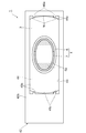
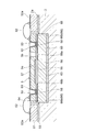
- FIG. 8 is a plan view of a second embodiment of the spectroscopic module according to the present invention
- FIG. 9 is a cross-sectional view taken along the line IX-IX in FIG.
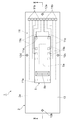
- the spectroscopic module 10 includes a substrate (main body portion) 2 that transmits light L1 incident from the front surface (one surface) 2a side, and a lens that transmits light L1 incident on the substrate 2.
- a part (main body part) 3 a spectroscopic part 4 that splits and reflects the light L 1 incident on the lens part 3, and a light detection element 5 that detects the light L 2 reflected by the spectroscopic part 4.
- the substrate 2 is formed in a rectangular plate shape, and a rectangular plate-like wiring substrate 51 in which an opening 51a having a rectangular cross section in which the light detection element 5 is disposed is formed on the front surface 2a of the substrate 2 is a resin agent. 53 is adhered.
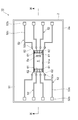
- the wiring board 51 is provided with a wiring 52 made of a metal material.
- the wiring 52 includes a plurality of pad portions 52a disposed around the opening 51a, a plurality of pad portions 52b disposed at both ends in the longitudinal direction of the wiring substrate 51, and a corresponding pad portion 52a and pad portion 52b.
- a plurality of connection portions 52c to be connected are provided.
- FIG. 10 is a bottom view of the spectral module of FIG.
- the lens portion 3 is formed on the substrate 2 by an optical resin agent 16 that transmits light L ⁇ b> 1 and L ⁇ b> 2 with the outer edge portion of the substrate 2 as a reference portion, such as corners and side portions of the substrate 2. It is bonded to the rear surface (the other surface) 2b.
- the outer edge portion of the substrate 2 serves as a reference unit for positioning the spectroscopic unit 4 on the substrate 2.
- the spectroscopic unit 4 includes a diffraction layer 6 formed on the outer surface of the lens unit 3, a reflection layer 7 formed on the outer surface of the diffraction layer 6, and a reflection layer 54 that covers the diffraction layer 6 and the reflection layer 7. It is a grating.
- the diffractive layer 6 is formed by arranging a plurality of grating grooves 6 a along the longitudinal direction of the substrate 2, and the extending direction of the grating grooves 6 a substantially coincides with the direction substantially orthogonal to the longitudinal direction of the substrate 2. To do.
- the light detection element 5 is formed in a rectangular plate shape, and a light detection part 5a is formed on the surface of the light detection element 5 on the spectroscopic part 4 side.
- the light detection unit 5a is a CCD image sensor, a PD array, a CMOS image sensor, or the like, and a direction in which a plurality of channels are substantially orthogonal to the extending direction of the grating grooves 6a of the spectroscopic unit 4 (that is, the parallel arrangement direction of the grating grooves 6a).
- the light detection element 5 is formed with a light passage hole 5b that is arranged in parallel with the light detection unit 5a in the channel arrangement direction and through which the light L1 traveling to the spectroscopic unit 4 passes.
- the light passage hole 5b is a slit extending in a direction substantially orthogonal to the longitudinal direction of the substrate 2, and is formed by etching or the like while being positioned with high accuracy with respect to the light detection portion 5a.
- the light shielding film 57 shields the light L1 that is about to travel to the spectroscopic unit 4 without passing through the light passage hole 5b and the light L1 that is about to be directly incident on the light detection unit 5a. Similar to the light shielding film 57, the wiring substrate 51 also has a function of shielding the light L1 that is about to travel to the spectroscopic unit 4 without passing through the light passage hole 5b.
- a plurality of electrodes 58 are formed on the surface of the photodetecting element 5 on the spectroscopic unit 4 side, and the surface of the photodetecting element 5 opposite to the spectroscopic unit 4 is connected to each electrode 58 and a through electrode 59.
- a plurality of terminal electrodes 61 are formed. Each terminal electrode 61 is connected to the corresponding pad portion 52 a of the wiring substrate 51 by a wire 62. Thereby, the electric signal generated in the light detection unit 5a is extracted to the outside through the electrode 58, the through electrode 59, the terminal electrode 61, the pad unit 52a, the connection unit 52c, and the pad unit 52b.
- An absorption layer 68 is formed on the surface of the light transmission plate 56 on the side of the light detection element 5.
- a light passage hole 68a is formed at a position facing the light passage hole 5b of the light detection element 5 so that the light L1 traveling to the spectroscopic unit 4 passes, and light detection of the light detection element 5 is performed.
- a light passage hole 68b is formed at a position facing the light detection portion 5a so that the light L2 traveling to the portion 5a passes therethrough.
- the light absorption layer 68 is patterned into a predetermined shape, and is integrally formed of CrO, a laminated film containing CrO, a black resist, or the like.
- the light absorption layer 68 may be formed on the surface of the light detection element 5 on the spectroscopic unit 4 side, as shown in FIG.
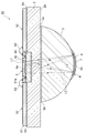
- the front surface 2a of the substrate 2 is provided with a concave section 64 having a rectangular cross section in which the light detecting element 5 is fitted through an optical resin agent 63 that transmits light L1 and L2.
- the recess 64 includes a bottom surface 65 that is substantially parallel to the front surface 2 a of the substrate 2 and a side wall 66 that is substantially perpendicular to the bottom surface 65, with respect to the outer edge portion of the substrate 2 that serves as a reference portion for positioning the spectroscopic unit 4 on the substrate 2. And formed by etching so as to have a predetermined positional relationship. Note that the light detection element 5 protrudes from the front surface 2 a of the substrate 2 in a state of being fitted in the recess 64.
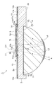
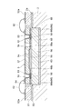
- FIG. 13 is a diagram showing the relationship between the light detection element and the recess in the spectroscopic module of FIG.
- the concave portion 64 includes a side wall (third fitting portion) 66 a that fits with the light detection element 5 in the extending direction of the grating groove 6 a of the spectroscopic unit 4, and the grating of the spectroscopic unit 4.
- a side wall (fourth fitting portion) 66b that is fitted to the light detection element 5 is provided in a direction substantially orthogonal to the extending direction of the groove 6a.
- the gap between the side wall 66b and the light detection element 5 is smaller than the gap between the side wall 66a and the light detection element 5.
- the spectroscopic unit 4 is formed in the lens unit 3. Specifically, a light transmissive master grating in which a grating corresponding to the diffraction layer 6 is engraved is pressed against the replica optical resin dropped near the apex of the lens unit 3. Then, the optical resin for replica is cured by irradiating light in this state, and preferably, the diffraction layer 6 having a plurality of grating grooves 6a is formed by performing heat curing for stabilization.
- a reflective layer 7 is formed by depositing Al, Au or the like on the outer surface of the diffracting layer 6, further the MgF 2 or the like on the outer surface of the diffracting layer 6 and reflecting layer 7
- the passivation layer 54 is formed by vapor deposition.
- the outer edge portion of the substrate 2 such as a corner portion or a side portion of the substrate 2 is used as a reference portion with respect to the reference portion.
- the recess 64 is formed in the front surface 2a of the substrate 2 so as to have a predetermined positional relationship.
- the lens part 3 on which the spectroscopic part 4 is formed is adhered to the rear surface 2b of the substrate 2 by the optical resin agent 16 with the outer edge part of the substrate 2 as a reference part, such as corners and side parts of the substrate 2.
- the optical resin agent 63 is applied to the concave portion 64 of the substrate 2, and the photodetector 5 with the light transmission plate 56 is fitted into the concave portion 64.
- the optical resin agent 63 is cured by irradiating light, and the photodetecting element 5 is mounted on the substrate 2.
- the wiring board 51 is bonded to the front surface 2 a of the board 2 with the resin agent 53. Then, the corresponding terminal electrode 61 of the light detection element 5 and the pad portion 52a of the wiring substrate 51 are connected by the wire 62, and the spectroscopic module 10 is obtained.
- the concave portion 64 has a predetermined positional relationship with the outer edge portion of the substrate 2, which is a reference portion for positioning the spectroscopic portion 4 on the substrate 2.
- the light detection element 5 is positioned on the substrate 2 only by fitting the detection element 5 into the recess 64.
- the lens unit 3 on which the spectroscopic unit 4 is formed is positioned on the substrate 2 by the outer edge portion of the substrate 2 which is a reference unit. As a result, alignment of the spectroscopic unit 4 and the light detection element 5 is realized.
- the light detection element 5 is in the shape of a rectangular plate, the gap between the light detection element 5 and the side wall 66 of the recess 64 is formed longer in the extending direction of the grating groove 6a, and the distance to the gap is further increased. Therefore, when the photodetecting element 5 is bonded to the substrate 2 by the optical resin agent 63, excess resin and air can be effectively released. Thus, according to the spectroscopic module 10, since so-called passive alignment is realized, it is possible to easily assemble while maintaining reliability.
- the light detection element 5 protrudes from the front surface 2 a of the substrate 2 in a state of being fitted in the recess 64.
- the light detection element 5 is reliably pressed against the bottom surface 65 of the concave portion 64, and an extra portion is obtained. Resin and air can be surely escaped.
- the light detection element 5 is provided with a light passage hole 5b through which the light L1 traveling to the spectroscopic unit 4 passes. Thereby, passive alignment of the light passage hole 5b with respect to the spectroscopic unit 4 and the light detection element 5 can be realized.
- the light passing hole 67a of the light L1 passes to proceeding to the spectroscopic unit 4, and the photodetector 5
- You may form the light absorption layer 67 which has the light passage hole 67b through which the light L2 which advances to the photon detection part 5a passes. According to this configuration, it is possible to limit the light that travels while spreading so as to reach a desired region, and it is possible to effectively suppress the stray light from entering the light detection element 5.
- the light absorbing layer 67 may be made of black resist, colored resin (silicone, epoxy, acrylic, urethane, polyimide, composite resin, etc.) containing filler (carbon, oxide, etc.), metal such as Cr or Co, or Examples thereof include metal oxides, laminated films thereof, porous ceramics, metals, and metal oxides. Further, the optical NA can be adjusted by changing the sizes of the light passage holes 67a and 67b in the light absorption layer 67.
- a so-called back-illuminated type element may be applied as the light detecting element 5.
- the electrode 58 since the electrode 58 is located on the outside together with the light detection portion 5a, the electrode 58 may be connected to the pad portion 52a of the wiring substrate 51 by the wire 62 using the electrode 58 as a terminal electrode.
- the substrate 2 and the lens part 3 may be integrally formed by molding, or the lens part 3 and the diffraction layer 6 may be integrally formed by a light-transmitting low melting point glass for replica molding.
- the concave portion 64 may be formed on the front surface of the lens portion 3 without using the substrate 2 as the main body portion.
- the side wall 66 of the recess 64 into which the light detection element 5 is fitted may have a separation portion 66 c that is separated from the light detection element 5.
- the present invention is not limited to the first and second embodiments described above, and the concave portion 19 is provided on the rear surface 2b of the substrate 2, and the lens portion 3 is provided in the concave portion 19 with the optical resin agent 16 interposed therebetween.
- the concave portion 64 may be provided on the front surface 2 a of the substrate 2, and the optical detection agent 5 may be fitted into the concave portion 64 with the optical resin agent 63 interposed therebetween.
- the concave portion 64 serves as a reference portion for positioning the light detection element 5 on the substrate 2
- the concave portion 19 serves as a reference portion for positioning the spectroscopic portion 4 on the substrate 2.
- the light passage hole 5b through which the light L1 traveling to the spectroscopic unit 4 passes may not be formed in the light detection element 5, but may be separately formed in a wiring board or a light shielding film.
- the present invention it is possible to easily assemble the spectral module while maintaining the reliability of the spectral module.
Landscapes
- Physics & Mathematics (AREA)
- Spectroscopy & Molecular Physics (AREA)
- General Physics & Mathematics (AREA)
- Optics & Photonics (AREA)
- Engineering & Computer Science (AREA)
- Manufacturing & Machinery (AREA)
- Spectrometry And Color Measurement (AREA)
Priority Applications (4)
| Application Number | Priority Date | Filing Date | Title |
|---|---|---|---|
| US12/992,398 US8804118B2 (en) | 2008-05-15 | 2009-05-07 | Spectral module |
| EP09746522.3A EP2287574B1 (en) | 2008-05-15 | 2009-05-07 | Spectral module |
| CN200980117552.8A CN102027343B (zh) | 2008-05-15 | 2009-05-07 | 分光模块 |
| KR1020167011626A KR101774186B1 (ko) | 2008-05-15 | 2009-05-07 | 분광모듈 |
Applications Claiming Priority (4)
| Application Number | Priority Date | Filing Date | Title |
|---|---|---|---|
| JP2008128687 | 2008-05-15 | ||
| JP2008-128687 | 2008-05-15 | ||
| JP2008-311057 | 2008-12-05 | ||
| JP2008311057A JP5205241B2 (ja) | 2008-05-15 | 2008-12-05 | 分光モジュール |
Publications (1)
| Publication Number | Publication Date |
|---|---|
| WO2009139315A1 true WO2009139315A1 (ja) | 2009-11-19 |
Family
ID=41318686
Family Applications (1)
| Application Number | Title | Priority Date | Filing Date |
|---|---|---|---|
| PCT/JP2009/058617 WO2009139315A1 (ja) | 2008-05-15 | 2009-05-07 | 分光モジュール |
Country Status (6)
Cited By (1)
| Publication number | Priority date | Publication date | Assignee | Title |
|---|---|---|---|---|
| EP2584956B1 (de) * | 2010-06-22 | 2021-08-04 | Sentec GmbH | Vorrichtung und verfahren zum erkennen und überwachen von physiologischen blutwerten |
Families Citing this family (9)
| Publication number | Priority date | Publication date | Assignee | Title |
|---|---|---|---|---|
| JP6234667B2 (ja) * | 2012-08-06 | 2017-11-22 | 浜松ホトニクス株式会社 | 光学素子及びその製造方法 |
| EP2857810A1 (en) * | 2013-10-02 | 2015-04-08 | Nederlandse Organisatie voor toegepast -natuurwetenschappelijk onderzoek TNO | Monolith spectrometer |
| JP2015106106A (ja) | 2013-12-02 | 2015-06-08 | セイコーエプソン株式会社 | 電子デバイスおよび電子機器 |
| JP6251073B2 (ja) * | 2014-02-05 | 2017-12-20 | 浜松ホトニクス株式会社 | 分光器、及び分光器の製造方法 |
| JP6395389B2 (ja) * | 2014-02-05 | 2018-09-26 | 浜松ホトニクス株式会社 | 分光器 |
| US9863809B2 (en) | 2015-08-31 | 2018-01-09 | Mettler-Toledo Gmbh | Spectrograph |
| EP3372966B1 (en) * | 2017-03-10 | 2021-09-01 | Hitachi High-Tech Analytical Science Limited | A portable analyzer using optical emission spectoscopy |
| US11639873B2 (en) * | 2020-04-15 | 2023-05-02 | Viavi Solutions Inc. | High resolution multi-pass optical spectrum analyzer |
| CN113782644B (zh) * | 2021-11-12 | 2022-01-25 | 同方威视技术股份有限公司 | 太赫兹探测装置的制造方法及探测设备 |
Citations (6)
| Publication number | Priority date | Publication date | Assignee | Title |
|---|---|---|---|---|
| JPH04294223A (ja) | 1990-12-04 | 1992-10-19 | Carl Zeiss:Fa | ダイオード列型分光分析器 |
| DE19717015A1 (de) * | 1997-04-23 | 1998-10-29 | Inst Mikrotechnik Mainz Gmbh | Miniaturisiertes optisches Bauelement sowie Verfahren zu seiner Herstellung |
| JP2592081Y2 (ja) * | 1993-08-13 | 1999-03-17 | 信越化学工業株式会社 | 光学素子の固定部品およびそれを応用した光アイソレータ |
| JP2000065642A (ja) | 1998-03-11 | 2000-03-03 | Gretag Macbeth Ag | スペクトロメ―タ |
| JP2004354176A (ja) | 2003-05-28 | 2004-12-16 | Hamamatsu Photonics Kk | 光検出器及びそれを用いた分光器 |
| WO2008149940A1 (ja) * | 2007-06-08 | 2008-12-11 | Hamamatsu Photonics K.K. | 分光モジュール |
Family Cites Families (70)
| Publication number | Priority date | Publication date | Assignee | Title |
|---|---|---|---|---|
| US4259014A (en) | 1979-04-03 | 1981-03-31 | Princeton Applied Research Corporation | Fiber optic polychromator |
| DE3509131A1 (de) | 1985-03-14 | 1986-09-18 | Fa. Carl Zeiss, 7920 Heidenheim | Verfahren zur justierten montage der optischen bauteile eines optischen geraetes |
| JP2592081B2 (ja) | 1987-12-28 | 1997-03-19 | スズキ株式会社 | 自動二輪車等のマフラ |
| JPH04287001A (ja) | 1991-03-15 | 1992-10-12 | Sekinosu Kk | 光回折格子の製造方法 |
| JPH06167637A (ja) | 1992-11-30 | 1994-06-14 | Hitachi Ltd | 多芯光コネクタ |
| JPH08145794A (ja) | 1994-11-17 | 1996-06-07 | Shimadzu Corp | 分光器 |
| US6224912B1 (en) | 1996-04-03 | 2001-05-01 | The Rogo Institute | Cancer-cell proliferation-suppressing material produced by cancer cells restricted by entrapment |
| US5995221A (en) | 1997-02-28 | 1999-11-30 | Instruments S.A., Inc. | Modified concentric spectrograph |
| US6303934B1 (en) | 1997-04-10 | 2001-10-16 | James T. Daly | Monolithic infrared spectrometer apparatus and methods |
| DE19717014A1 (de) | 1997-04-23 | 1998-10-29 | Inst Mikrotechnik Mainz Gmbh | Verfahren und Form zur Herstellung miniaturisierter Formenkörper |
| AU5068098A (en) | 1997-11-28 | 1999-06-16 | Hamamatsu Photonics K.K. | Solid state image pickup device and analyzer using it |
| US6608679B1 (en) | 1998-12-21 | 2003-08-19 | Xerox Corporation | Spectrophotometric analysis of input light |
| US6249346B1 (en) | 1998-12-21 | 2001-06-19 | Xerox Corporation | Monolithic spectrophotometer |
| JP2000269472A (ja) | 1999-03-15 | 2000-09-29 | Canon Inc | 撮像装置 |
| DE59913150D1 (de) | 1999-04-01 | 2006-04-27 | Gretag Macbeth Ag Regensdorf | Spektrometer |
| JP4287001B2 (ja) | 1999-10-27 | 2009-07-01 | 帝人株式会社 | 透明導電積層体 |
| US6538736B1 (en) | 1999-12-01 | 2003-03-25 | Hach Company | Concentric spectrometer with mitigation of internal specular reflections |
| AU2001276875A1 (en) | 2000-07-11 | 2002-01-21 | Ibsen Photonics | Monitoring apparatus for optical transmission systems |
| CN1296684C (zh) | 2000-07-28 | 2007-01-24 | 大塚电子株式会社 | 光谱检测设备 |
| US6657723B2 (en) * | 2000-12-13 | 2003-12-02 | International Business Machines Corporation | Multimode planar spectrographs for wavelength demultiplexing and methods of fabrication |
| US7002697B2 (en) | 2001-08-02 | 2006-02-21 | Aegis Semiconductor, Inc. | Tunable optical instruments |
| JP2003139611A (ja) | 2001-11-06 | 2003-05-14 | Olympus Optical Co Ltd | 分光光度計 |
| JP3912111B2 (ja) | 2002-01-09 | 2007-05-09 | 富士通株式会社 | 波長多重双方向光伝送モジュール |
| JP3818441B2 (ja) | 2002-02-20 | 2006-09-06 | 日本電信電話株式会社 | 基板実装構造及び半導体装置 |
| JP4221965B2 (ja) * | 2002-07-22 | 2009-02-12 | 日立電線株式会社 | 回折格子、波長合分波器及びこれらを用いた波長多重信号光伝送モジュール |
| US6885107B2 (en) | 2002-08-29 | 2005-04-26 | Micron Technology, Inc. | Flip-chip image sensor packages and methods of fabrication |
| US7170600B2 (en) | 2002-09-20 | 2007-01-30 | Nippon Sheet Glass Company, Limited | Spectrometer using diffraction grating |
| FR2847978B1 (fr) | 2002-12-02 | 2005-12-02 | Technologie Optique Et Etudes | Spectrometre compact a composant optique monolithique |
| JP2004191246A (ja) | 2002-12-12 | 2004-07-08 | Matsushita Electric Ind Co Ltd | 凹凸検出センサ |
| DE10304312A1 (de) | 2003-02-04 | 2004-08-12 | Carl Zeiss Jena Gmbh | Kompakt-Spektrometer |
| CN101373783B (zh) | 2003-03-10 | 2010-06-23 | 浜松光子学株式会社 | 光电二极管阵列及其制造方法 |
| JP2004309146A (ja) | 2003-04-02 | 2004-11-04 | Olympus Corp | 分光光度計 |
| US7283233B1 (en) | 2004-03-20 | 2007-10-16 | Seng-Tiong Ho | Curved grating spectrometer with very high wavelength resolution |
| US7623235B2 (en) | 2004-03-20 | 2009-11-24 | Seng-Tiong Ho | Curved grating spectrometer with very high wavelength resolution |
| JP4627410B2 (ja) | 2004-04-20 | 2011-02-09 | 浜松ホトニクス株式会社 | 分光器を用いた測定装置 |
| JP4720120B2 (ja) | 2004-07-14 | 2011-07-13 | ソニー株式会社 | 半導体イメージセンサ・モジュール |
| JP4473665B2 (ja) | 2004-07-16 | 2010-06-02 | 浜松ホトニクス株式会社 | 分光器 |
| WO2006010367A2 (en) | 2004-07-26 | 2006-02-02 | Danmarks Tekniske Universitet | On-chip spectroscopy |
| JP4576961B2 (ja) | 2004-09-28 | 2010-11-10 | 株式会社島津製作所 | レプリカ回折格子の製造方法 |
| JP2006322841A (ja) | 2005-05-19 | 2006-11-30 | Shimadzu Corp | 分光測定方法及び分光光度計 |
| US7330258B2 (en) | 2005-05-27 | 2008-02-12 | Innovative Technical Solutions, Inc. | Spectrometer designs |
| US7289220B2 (en) | 2005-10-14 | 2007-10-30 | Board Of Regents, The University Of Texas System | Broadband cavity spectrometer apparatus and method for determining the path length of an optical structure |
| JP4811032B2 (ja) | 2006-01-30 | 2011-11-09 | 株式会社島津製作所 | 反射型レプリカ光学素子 |
| US7697137B2 (en) | 2006-04-28 | 2010-04-13 | Corning Incorporated | Monolithic Offner spectrometer |
| EP1882916A1 (en) | 2006-07-20 | 2008-01-30 | Interuniversitair Microelektronica Centrum | Compact catadioptric spectrometer |
| WO2008029852A1 (fr) | 2006-09-06 | 2008-03-13 | Nikon Corporation | Dispositif optique, appareil d'exposition et procédé de fabrication du dispositif |
| JP4490406B2 (ja) | 2006-10-11 | 2010-06-23 | 浜松ホトニクス株式会社 | 固体撮像装置 |
| JP4905193B2 (ja) | 2007-03-16 | 2012-03-28 | コニカミノルタセンシング株式会社 | 凹面回折ミラー及びこれを用いた分光装置 |
| JP4891841B2 (ja) | 2007-06-08 | 2012-03-07 | 浜松ホトニクス株式会社 | 分光モジュール |
| EP2072978A4 (en) | 2007-06-08 | 2014-01-08 | Hamamatsu Photonics Kk | SPECTROSCOPIC MODULE |
| CN101542251B (zh) | 2007-06-08 | 2012-09-26 | 浜松光子学株式会社 | 分光器 |
| TWI342862B (en) | 2008-01-31 | 2011-06-01 | Univ Nat Taiwan | Method of micro/nano imprinting |
| CN102628711B (zh) | 2008-03-04 | 2016-01-20 | 浜松光子学株式会社 | 分光模块 |
| JP5111163B2 (ja) | 2008-03-04 | 2012-12-26 | 浜松ホトニクス株式会社 | 分光器 |
| JP5205240B2 (ja) | 2008-05-15 | 2013-06-05 | 浜松ホトニクス株式会社 | 分光モジュールの製造方法及び分光モジュール |
| JP5512961B2 (ja) | 2008-05-15 | 2014-06-04 | 浜松ホトニクス株式会社 | 分光モジュール及びその製造方法 |
| JP5074291B2 (ja) | 2008-05-15 | 2012-11-14 | 浜松ホトニクス株式会社 | 分光モジュール |
| JP5207938B2 (ja) | 2008-05-15 | 2013-06-12 | 浜松ホトニクス株式会社 | 分光モジュール及び分光モジュールの製造方法 |
| JP5415060B2 (ja) | 2008-05-15 | 2014-02-12 | 浜松ホトニクス株式会社 | 分光モジュール |
| JP5205242B2 (ja) | 2008-05-15 | 2013-06-05 | 浜松ホトニクス株式会社 | 分光器の製造方法 |
| JP5205239B2 (ja) | 2008-05-15 | 2013-06-05 | 浜松ホトニクス株式会社 | 分光器 |
| JP5205238B2 (ja) | 2008-05-15 | 2013-06-05 | 浜松ホトニクス株式会社 | 分光モジュール |
| JP5205243B2 (ja) | 2008-05-15 | 2013-06-05 | 浜松ホトニクス株式会社 | 分光器 |
| JP2009300418A (ja) | 2008-05-15 | 2009-12-24 | Hamamatsu Photonics Kk | 分光モジュール |
| JP5411778B2 (ja) | 2009-04-30 | 2014-02-12 | キヤノン株式会社 | 分光測色装置、およびそれを用いた画像形成装置 |
| JP2010261767A (ja) | 2009-05-01 | 2010-11-18 | Canon Inc | 分光装置及びそれを有する画像形成装置 |
| JP5669434B2 (ja) | 2009-05-09 | 2015-02-12 | キヤノン株式会社 | 回折素子及び回折素子の製造方法及びそれを用いた分光器 |
| JP5421684B2 (ja) | 2009-07-29 | 2014-02-19 | キヤノン株式会社 | 回折光学素子、それを用いた分光測色装置および画像形成装置 |
| DE102009046831B4 (de) | 2009-11-18 | 2015-02-12 | Fraunhofer-Gesellschaft zur Förderung der angewandten Forschung e.V. | Strahlungserzeugungsvorrichtung zum Erzeugen einer elektromagnetischen Strahlung mit einer einstellbaren spektralen Zusammensetzung und Verfahren zur Herstellung derselben |
| JP5335729B2 (ja) | 2010-04-01 | 2013-11-06 | 浜松ホトニクス株式会社 | 分光モジュール |
-
2008
- 2008-12-05 JP JP2008311057A patent/JP5205241B2/ja active Active
-
2009
- 2009-05-07 KR KR1020107015306A patent/KR20110005771A/ko not_active Ceased
- 2009-05-07 US US12/992,398 patent/US8804118B2/en active Active
- 2009-05-07 EP EP09746522.3A patent/EP2287574B1/en active Active
- 2009-05-07 CN CN200980117552.8A patent/CN102027343B/zh active Active
- 2009-05-07 WO PCT/JP2009/058617 patent/WO2009139315A1/ja active Application Filing
- 2009-05-07 KR KR1020167011626A patent/KR101774186B1/ko active Active
Patent Citations (6)
| Publication number | Priority date | Publication date | Assignee | Title |
|---|---|---|---|---|
| JPH04294223A (ja) | 1990-12-04 | 1992-10-19 | Carl Zeiss:Fa | ダイオード列型分光分析器 |
| JP2592081Y2 (ja) * | 1993-08-13 | 1999-03-17 | 信越化学工業株式会社 | 光学素子の固定部品およびそれを応用した光アイソレータ |
| DE19717015A1 (de) * | 1997-04-23 | 1998-10-29 | Inst Mikrotechnik Mainz Gmbh | Miniaturisiertes optisches Bauelement sowie Verfahren zu seiner Herstellung |
| JP2000065642A (ja) | 1998-03-11 | 2000-03-03 | Gretag Macbeth Ag | スペクトロメ―タ |
| JP2004354176A (ja) | 2003-05-28 | 2004-12-16 | Hamamatsu Photonics Kk | 光検出器及びそれを用いた分光器 |
| WO2008149940A1 (ja) * | 2007-06-08 | 2008-12-11 | Hamamatsu Photonics K.K. | 分光モジュール |
Cited By (1)
| Publication number | Priority date | Publication date | Assignee | Title |
|---|---|---|---|---|
| EP2584956B1 (de) * | 2010-06-22 | 2021-08-04 | Sentec GmbH | Vorrichtung und verfahren zum erkennen und überwachen von physiologischen blutwerten |
Also Published As
| Publication number | Publication date |
|---|---|
| KR101774186B1 (ko) | 2017-09-01 |
| KR20160056945A (ko) | 2016-05-20 |
| JP5205241B2 (ja) | 2013-06-05 |
| US8804118B2 (en) | 2014-08-12 |
| EP2287574A4 (en) | 2014-01-08 |
| EP2287574A1 (en) | 2011-02-23 |
| US20110164247A1 (en) | 2011-07-07 |
| JP2009300419A (ja) | 2009-12-24 |
| CN102027343A (zh) | 2011-04-20 |
| EP2287574B1 (en) | 2020-06-17 |
| KR20110005771A (ko) | 2011-01-19 |
| CN102027343B (zh) | 2014-03-19 |
Similar Documents
| Publication | Publication Date | Title |
|---|---|---|
| JP5205241B2 (ja) | 分光モジュール | |
| JP5415060B2 (ja) | 分光モジュール | |
| JP5207938B2 (ja) | 分光モジュール及び分光モジュールの製造方法 | |
| JP5512961B2 (ja) | 分光モジュール及びその製造方法 | |
| JP5205238B2 (ja) | 分光モジュール | |
| JP5325829B2 (ja) | 分光モジュール | |
| JP5335729B2 (ja) | 分光モジュール | |
| JP5205240B2 (ja) | 分光モジュールの製造方法及び分光モジュール | |
| US8013993B2 (en) | Spectroscopy module | |
| TWI470193B (zh) | Spectral module | |
| JP5074291B2 (ja) | 分光モジュール | |
| JP5235250B2 (ja) | 分光モジュール | |
| JP2009300417A (ja) | 分光モジュールの製造方法及び分光モジュール | |
| JP2013007707A (ja) | 分光モジュール |
Legal Events
| Date | Code | Title | Description |
|---|---|---|---|
| WWE | Wipo information: entry into national phase |
Ref document number: 200980117552.8 Country of ref document: CN |
|
| 121 | Ep: the epo has been informed by wipo that ep was designated in this application |
Ref document number: 09746522 Country of ref document: EP Kind code of ref document: A1 |
|
| ENP | Entry into the national phase |
Ref document number: 20107015306 Country of ref document: KR Kind code of ref document: A |
|
| NENP | Non-entry into the national phase |
Ref country code: DE |
|
| WWE | Wipo information: entry into national phase |
Ref document number: 2009746522 Country of ref document: EP |
|
| WWE | Wipo information: entry into national phase |
Ref document number: 12992398 Country of ref document: US |