WO2009118944A1 - 異方性導電膜転写具及び接続方法 - Google Patents
異方性導電膜転写具及び接続方法 Download PDFInfo
- Publication number
- WO2009118944A1 WO2009118944A1 PCT/JP2008/070546 JP2008070546W WO2009118944A1 WO 2009118944 A1 WO2009118944 A1 WO 2009118944A1 JP 2008070546 W JP2008070546 W JP 2008070546W WO 2009118944 A1 WO2009118944 A1 WO 2009118944A1
- Authority
- WO
- WIPO (PCT)
- Prior art keywords
- anisotropic conductive
- conductive film
- tape
- reel
- take
- Prior art date
- Legal status (The legal status is an assumption and is not a legal conclusion. Google has not performed a legal analysis and makes no representation as to the accuracy of the status listed.)
- Ceased
Links
Images



Classifications
-
- H—ELECTRICITY
- H05—ELECTRIC TECHNIQUES NOT OTHERWISE PROVIDED FOR
- H05K—PRINTED CIRCUITS; CASINGS OR CONSTRUCTIONAL DETAILS OF ELECTRIC APPARATUS; MANUFACTURE OF ASSEMBLAGES OF ELECTRICAL COMPONENTS
- H05K3/00—Apparatus or processes for manufacturing printed circuits
- H05K3/30—Assembling printed circuits with electric components, e.g. with resistors
- H05K3/32—Assembling printed circuits with electric components, e.g. with resistors electrically connecting electric components or wires to printed circuits
- H05K3/321—Assembling printed circuits with electric components, e.g. with resistors electrically connecting electric components or wires to printed circuits by conductive adhesives
- H05K3/323—Assembling printed circuits with electric components, e.g. with resistors electrically connecting electric components or wires to printed circuits by conductive adhesives by applying an anisotropic conductive adhesive layer over an array of pads
-
- B—PERFORMING OPERATIONS; TRANSPORTING
- B65—CONVEYING; PACKING; STORING; HANDLING THIN OR FILAMENTARY MATERIAL
- B65H—HANDLING THIN OR FILAMENTARY MATERIAL, e.g. SHEETS, WEBS, CABLES
- B65H37/00—Article or web delivery apparatus incorporating devices for performing specified auxiliary operations
- B65H37/002—Web delivery apparatus, the web serving as support for articles, material or another web
- B65H37/005—Hand-held apparatus
- B65H37/007—Applicators for applying coatings, e.g. correction, colour or adhesive coatings
-
- B—PERFORMING OPERATIONS; TRANSPORTING
- B65—CONVEYING; PACKING; STORING; HANDLING THIN OR FILAMENTARY MATERIAL
- B65H—HANDLING THIN OR FILAMENTARY MATERIAL, e.g. SHEETS, WEBS, CABLES
- B65H2701/00—Handled material; Storage means
- B65H2701/30—Handled filamentary material
- B65H2701/37—Tapes
-
- H—ELECTRICITY
- H05—ELECTRIC TECHNIQUES NOT OTHERWISE PROVIDED FOR
- H05K—PRINTED CIRCUITS; CASINGS OR CONSTRUCTIONAL DETAILS OF ELECTRIC APPARATUS; MANUFACTURE OF ASSEMBLAGES OF ELECTRICAL COMPONENTS
- H05K2203/00—Indexing scheme relating to apparatus or processes for manufacturing printed circuits covered by H05K3/00
- H05K2203/01—Tools for processing; Objects used during processing
- H05K2203/0104—Tools for processing; Objects used during processing for patterning or coating
- H05K2203/0126—Dispenser, e.g. for solder paste, for supplying conductive paste for screen printing or for filling holes
Definitions
- the present invention relates to an anisotropic conductive film transfer tool for supplying an anisotropic conductive film to a connection region when an electronic component such as an IC chip is anisotropically connected to a wiring board.
- the reel with the anisotropic conductive tape wound around was used by attaching it to a large automatic temporary sticking device.
- the shape of the region is complicated, there is a problem that it is difficult to set the temporary sticking conditions of the automatic temporary sticking apparatus.
- the increase in the types of shape of the connection area has also hindered the operation of the automatic temporary sticking apparatus.
- the transfer tool of Patent Document 1 since a film-like adhesive such as an anisotropic conductive film to be used is not referred to as a transfer tool-specific adhesive, a film-like type that is temporarily attached by conventional thermocompression bonding. It must be considered that the premise is to use an adhesive. Accordingly, the transfer tool has to be provided with a heat generating part for heating the drawn film-like adhesive such as the anisotropic conductive film and the power supply part, which hinders downsizing of the transfer tool.
- the present invention is intended to solve the above-described problems of the prior art, and the anisotropic conductive tape of an anisotropic conductive tape comprising a base tape and an anisotropic conductive film formed on one surface thereof is provided.
- An object of the present invention is to provide a transfer tool that is not provided with a heat generating part or a power supply part so that it can be easily and temporarily attached to a transfer surface manually.
- the present inventor has found that the above-mentioned object can be achieved by setting the tensile fracture stress and the adhesive strength in the uncured state of the anisotropic conductive film constituting the anisotropic conductive tape to predetermined ranges, The present invention has been completed.
- the present invention relates to an anisotropic conductive film transfer tool for pressure-sensitive transfer of an anisotropic conductive film to a transfer surface from an anisotropic conductive tape in which the anisotropic conductive film is temporarily pasted on a base tape.
- An unwinding reel in which the anisotropic conductive tape is wound with the anisotropic conductive film on the outside A transfer head that presses the anisotropic conductive tape drawn from the unwinding reel to the transfer surface, and transfers the anisotropic conductive film to the transfer surface; The take-up reel that winds up the base tape after the anisotropic conductive film is transferred to the transfer surface, and the interlock that links the rotation of the take-up reel and take-up reel so that the anisotropic conductive tape does not loosen
- the anisotropic conductive film has an uncured tensile fracture stress according to JIS K7127 of 1.0 to 5.0 MPa and the anisotropic conductive film is transferred to a glass fiber reinforced epoxy plate, the uncured An anisotropic conductive film transfer tool having a 90 ° peel adhesion strength of 1.0 to 2.5 N / cm according to JIS K6854-1 in a state is provided.
- the present invention is a connection method for anisotropically conductively connecting an electronic component to a connection portion of a wiring board via an anisotropic conductive film,
- the anisotropic conductive tape is pulled out from the unwinding reel while pressing the anisotropic conductive film from the base tape side with the transfer head of the above-mentioned anisotropic conductive film transfer tool against the connection part of the wiring board.
- a connection method including a step of aligning an electronic component and performing a main thermocompression bonding on an anisotropic conductive film temporarily attached to a connection portion of a wiring board.
- the anisotropic conductive film transfer tool of the present invention since the tensile fracture stress and the adhesive strength of the uncured anisotropic conductive film constituting the anisotropic conductive tape are set within a predetermined range, Using a transfer tool that is not provided with a power supply unit or a power supply unit, it can be easily and temporarily attached to the transfer surface manually.
- FIG. 1 is a perspective view of an anisotropic conductive film transfer tool 1A of the present invention.
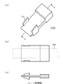
- FIG. 2 is a perspective view (a), a plan view (b), and a sectional view (c) of the transfer head 10A.
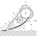
- FIG. 3 is an explanatory diagram of the transport system of the anisotropic conductive film transfer tool 1A of the present invention.
- FIG. 4 is a cross-sectional view of the anisotropic conductive tape.
- FIG. 5 is an explanatory view of an anisotropic conductive film transfer tool 1B according to another aspect of the present invention.
- FIG. 1 shows a book in which the interlocking mechanism is composed of a winding pulley provided coaxially with the winding reel, a winding pulley provided coaxially with the winding reel, and a belt for rotatably connecting them.
- FIG. 2 is a perspective view of an anisotropic conductive film transfer tool 1A according to an embodiment of the invention, and FIG. 2 is a perspective view of a plate-shaped transfer head 10A used in the anisotropic conductive film viscous transfer tool 1A. ), A plan view (b), and a cross-sectional view (c), and FIG. 3 is an explanatory diagram of a transport system of the anisotropic conductive film transfer tool 1A.
- FIG. 4 is a cross-sectional view of one embodiment of the anisotropic conductive tape 30 used in the anisotropic conductive film transfer tool 1A.
- the anisotropic conductive tape 30 in FIG. 4 can peel the anisotropic conductive film 32 on the surface of the base tape 31 that has been subjected to known peeling treatment or light adhesion treatment on the back surface and the front surface as necessary. Attached and held.
- the base tape 31 can be configured in the same manner as a base sheet of a known anisotropic conductive tape, and can be formed of, for example, a plastic material such as polyethylene terephthalate, polyethylene, or polypropylene, or a paper material. it can.
- the thickness of the base tape 31 is preferably 4 to 100 ⁇ m.
- the peeling treatment performed on the back surface of the base tape 31 is performed according to the forming material of the base tape 31, and for example, it is treated using a silicone release agent, a fluorine release agent, or the like. Can do.
- a release treatment layer is formed by the treatment, and an inorganic filler such as silica and alumina and resin particles such as polyethylene, polypropylene, nylon, fluororesin, and silicone resin may be appropriately blended in the release treatment layer.
- the peeling process or the light adhesion process performed on the surface of the base tape 31 is a process for sticking and holding the anisotropic conductive film 32 on the base tape 31.
- the adhesion strength or adhesion obtained by the treatment is weaker than the adhesion of the anisotropic conductive film 32 to the transfer surface. Therefore, the anisotropic conductive film 32 of the anisotropic conductive tape 30 is connected to the wiring circuit.
- the anisotropic conductive film transfer tool 1A is pulled away from the transfer surface S after being pressed against the transfer surface S such as the connection portion, the base tape 31 is easily peeled off from the anisotropic conductive film 32, and the anisotropic The conductive film 32 remains on the transfer surface S.
- a treatment with a silicone-based release agent or the like can be given as in the case of the back surface of the base tape 31.
- a light pressure-sensitive adhesive treatment for example, a light pressure-sensitive adhesive composition such as an acrylic pressure-sensitive adhesive is applied on the base tape 31 to form a light pressure-sensitive adhesive layer.
- the anisotropic conductive film 32 has a specific tensile fracture stress and adhesive strength in an uncured state so that the anisotropic conductive film 32 can be manually and easily transferred to the transfer surface using a transfer tool.
- the tensile fracture stress according to JIS K7127 of the anisotropic conductive film 32 in an uncured state is 1.0 to 5.0 MPa, preferably 1.0 to 2.0 MPa. Below this range, the anisotropic conductive film 32 cannot easily withstand the force applied during transfer to the adherend and cannot be pasted easily. When exceeding this range, more force is required when cutting. And cutting at a desired location becomes difficult.
- the 90 ° peel adhesion strength according to JIS K6854-1 in an uncured state is 1.0 to 2.5 N / cm, Preferably, it is 1.5 to 2.5 N / cm. Below this range, the adhesiveness to the adherend in the form of the present invention is insufficient and cannot be attached. On the other hand, if it is too high, it becomes difficult to remove the anisotropic conductive film 32 without any residue when the anisotropic conductive film 32 is peeled off due to an attachment mistake or the like.
- the anisotropic conductive film 32 is obtained by uniformly dissolving or dispersing known conductive particles, a latent curing agent, a silane coupling agent, polybutadiene rubber and the like in a known insulating binder such as a phenoxy resin or an epoxy resin. is there.
- a known insulating binder such as a phenoxy resin or an epoxy resin.
- known fillers and pigments such as fumed silica, titanium oxide, calcium carbonate, and talc are dispersed.
- the blending amount of the solid insulating binder should be 20% by mass or less, and the phenoxy resin has a biphenyl skeleton, a fluorene skeleton, etc. in the molecular structure. And it is preferable to use what has a high glass transition point, and to make the compounding quantity of fillers, such as a fumed silica, into 4 mass% or more.
- the anisotropic conductive tape 30 as described above is obtained by applying the anisotropic conductive film 32 to a wide base tape by coating using a printing technique such as silk screen printing, various coaters such as reverse roll coating and direct coating. Can be manufactured by slitting to a predetermined width using a known slitter to a necessary width after drying.
- the anisotropic conductive film transfer tool 1A shown in FIG. 1 has, as its own structure, a winding wound around the case 2 with the anisotropic conductive film 32 of the anisotropic conductive tape 30 on the outside.
- the take-out reel 3 is rotatably supported by the support shaft 5, and the take-up reel 6 for winding the base tape 31 after the anisotropic conductive film 32 is transferred to the transfer surface S can be rotated by the support shaft 8. It is supported by.
- the take-up reel 3 is provided with a take-up pulley 4 coaxially therewith, and the take-up reel 6 is provided with a take-up pulley 7 coaxially therewith.
- the take-up pulley 4 and the take-up pulley 7 are made of rubber or the like.
- the belt 9 is connected.
- the case 2 is fixed with a transfer head 10A that presses the anisotropic conductive tape 30 drawn from the unwinding reel 3 against the transfer surface S and transfers the anisotropic conductive film 32 to the transfer surface S. ing.
- the transfer head 10A is formed of a plate-like member having a tapered cross section that becomes gradually thinner toward the tip. Further, the width of the leading edge of the transfer head 10A is anisotropic so that the anisotropic conductive tape 30 can be used as it is even if the traveling position (broken line in the drawing) of the anisotropic conductive tape 30 is slightly shifted during use of the anisotropic conductive film transfer tool 1A.
- the guide flange 11 is formed on both side edges of the transfer head 10A so that the anisotropic conductive tape 30 does not come off the transfer head 10A.
- the transfer head 10A As a material for forming the transfer head 10A, it is preferable to use polystyrene, polypropylene, ABS, nylon, polyacetal (POM) or the like in order to uniformly apply the entire anisotropic conductive tape 30 to the transfer surface S.
- polystyrene polypropylene
- ABS polypropylene
- nylon polyacetal
- POM polyacetal
- reference numerals 12 and 13 are guide pins.
- a guide roller may be used instead of the guide pin.
- the case 2 is preferably excellent in portability with a size that fits in the palm.
- the transfer head 10 ⁇ / b> A is anisotropically moved by moving it in the direction of the arrow along the transfer surface S while pressing the transfer head 10 ⁇ / b> A.
- the conductive conductive film 32 is attached to the transfer surface S, and the anisotropic conductive tape 30 is pulled out from the unwinding reel 3.
- the take-up reel 6 connected to the take-up reel 3 by the pulleys 4 and 7 and the belt 9 rotates to pull the anisotropic conductive tape 30 and attach the anisotropic conductive film 32 to the transfer surface S.
- the base tape 31 is peeled off, and the base tape 31 after the anisotropic conductive film 32 is transferred to the transfer surface S is taken up on the take-up reel 6. Therefore, the anisotropic conductive film 32 can be simply attached to the transfer surface S. Further, if the anisotropic conductive film transfer tool 1A is lifted from the transfer surface S, the anisotropic conductive film 32 can be cut at substantially the tip of the transfer head 10A.
- the interlocking mechanism is composed of a winding pulley provided coaxially with the winding reel, a winding pulley provided coaxially with the winding reel, and a belt that rotatably couples them.
- the first spur gear 50 installed on the unwinding reel 3 so as to rotate at the same angular speed as shown in FIG.
- the interlocking mechanism may be configured by a second spur gear 60 which is installed so as to rotate at the same angular speed, meshed with the first spur gear 50 and has a fractional number than the first spur gear 50.
- Adjustment of the fraction of both spur gears can be appropriately performed so that the anisotropic conductive tape 30 can be pulled out without loosening and the base tape 31 can be wound up.
- the interlocking mechanism is not limited to these mechanisms, and any mechanism that can draw the anisotropic conductive tape without loosening and wind the base tape can be used.
- the anisotropic conductive film transfer tool of the present invention is preferably applied to a connection method in which an electronic component is anisotropically conductively connected to a connection portion of a wiring board via an anisotropic conductive film. it can.
- the anisotropic conductive film is pressed from the base tape side with the transfer head of the above-mentioned anisotropic conductive film transfer tool against the connection portion such as the connection pad of the wiring board such as the flexible wiring board and the glass substrate for the liquid crystal panel.
- the anisotropic conductive film transfer tool by moving the anisotropic conductive film transfer tool so that the anisotropic conductive tape is pulled out from the unwinding reel, the anisotropic conductive layer is transferred and temporarily pasted to the connection portion.
- the base tape from which the anisotropic conductive film has been peeled is wound, and on the other hand, an electronic component such as an IC chip is positioned and thermocompression bonded to the anisotropic conductive film temporarily attached to the connection portion of the wiring board.
- the wiring board and the electronic component can be easily and easily connected.
- Example 1-6 Comparative Example 1-2
- an anisotropic conductive composition was prepared by uniformly mixing the components shown in Table 1 according to a conventional method. Then, an anisotropic conductive sheet was prepared by applying the film to a dry thickness of 45 ⁇ m and drying. The resulting uncured anisotropic conductive film was evaluated for tensile fracture stress and 90-degree peel adhesion strength as described below. The obtained results are shown in Table 1.
- the obtained uncured anisotropic conductive sheet was further slit into a width of 2 mm to obtain an anisotropic conductive tape.
- An anisotropic conductive film transfer tool was prepared by mounting the obtained anisotropic conductive tape in place of a correction tape of a commercially available correction tape transfer tool (CT-PL2.5, Dragonfly Pencil Co., Ltd.). Using the obtained anisotropic conductive film transfer tool, as described below, the transferability of the anisotropic conductive film, the adhesive strength of the cured anisotropic conductive film, and the conduction resistance were tested and evaluated. The obtained results are shown in Table 1.
- ⁇ 90 degree peeling adhesive strength of uncured anisotropic conductive film JIS K6854-1)>
- the uncured anisotropic conductive film was cut out with a width of 25 mm, and pressed by reciprocating a 2 kg roller on a glass fiber reinforced epoxy plate at a pressing speed of 20 mm / sec.
- the uncured anisotropic conductive film was peeled in a direction perpendicular to the epoxy plate at a tensile speed of 50 mm / min using a tensile tester (Tensilon RTC-1210A, Orientec Co., Ltd.), and the force required for peeling was 90 ° peel adhesion strength.
- the 90 degree peel adhesive strength is desired to be 1.5 to 2.5 N / cm.
- ⁇ Adhesive strength of cured anisotropic conductive film The printed circuit board and the two-layer flexible board were thermocompression bonded through an anisotropic conductive film at 180 ° C. and a pressure of 3 MPa for 10 seconds.
- the adhesive strength of the cured anisotropic conductive film in this case was measured in the same manner as in the “90-degree peel adhesion strength of uncured anisotropic conductive film” test. That is, using a tensile tester (Tensilon RTC-1210A, Orientec Co., Ltd.), the two-layer flexible board was pulled at a rate of 50 mm / min in a direction of 90 degrees with respect to the printed circuit board, and the force required for this was measured as the adhesive strength. . Practically, it is desired to be 7 N / cm or more.
- the tensile fracture stress of the uncured anisotropic conductive film is in the range of 1.0 to 2.0 MPa and the 90 ° peel strength is in the range of 1.5 to 2.5 N / cm.
- the anisotropic conductive film transfer tool of Examples 1 to 4 can manually transfer the anisotropic conductive film. Moreover, it turns out that the characteristic of the adhesive strength and conduction
- the 90 degree peel adhesion strength of the uncured anisotropic conductive film was below 1.0 N / cm.
- the adhesive strength of the isotropic conductive film was also less than 7.0 N / cm, which was not sufficient, and as a result, a sufficient conduction resistance value could not be obtained.
- the anisotropic conductive film transfer tool of the present invention the tensile fracture stress and the adhesive strength of the anisotropic conductive film constituting the anisotropic conductive tape are set within a predetermined range. For this reason, the anisotropic conductive film transfer tool of the present invention can be used to easily and temporarily attach the anisotropic conductive tape to the transfer surface manually using a transfer tool that is not provided with a heat generating part or a power supply part. Therefore, it is useful as a manual transfer tool for anisotropic conductive tape.
Landscapes
- Engineering & Computer Science (AREA)
- Manufacturing & Machinery (AREA)
- Microelectronics & Electronic Packaging (AREA)
- Manufacturing Of Electrical Connectors (AREA)
- Wire Bonding (AREA)
- Electric Connection Of Electric Components To Printed Circuits (AREA)
- Combinations Of Printed Boards (AREA)
- Adhesives Or Adhesive Processes (AREA)
Abstract
基材テープ上に異方性導電膜が仮貼りされている異方性導電テープから該異方性導電膜を被転写面に感圧転写する異方性導電膜転写具は、異方性導電テープをその異方性導電膜を外側にして巻き回している巻出リール、巻出リールから引き出された異方性導電テープを被転写面に押圧し、異方性導電膜を被転写面に転写する転写ヘッド、異方性導電膜が被転写面に転写した後の基材テープを巻き取る巻取リール、及び巻出リールと巻取リールとの回転を、異方性導電テープが緩まないように連動させる連動機構を備え、異方性導電膜の未硬化の状態における引張破壊応力が1.0~5.0MPaであり、且つ異方性導電膜がガラス繊維強化エポキシ板に転写された場合に、未硬化の状態における90度剥離接着強さが1.0~2.5N/cmである。
Description
本発明は、ICチップ等の電子部品を配線基板に異方性接続する際に、それらの接続領域に異方性導電膜を供給するための異方性導電膜転写具に関する。
従来、異方性導電テープを接続部分に供給する場合、異方性導電テープを巻き回したリールを大型の自動仮貼装置に装着して使用していたが、接続部分が極めて小さい場合や接続領域の形状が複雑な場合には、自動仮貼装置の仮貼条件の設定が困難という問題があった。また、接続領域の形状の種類が増大していることも、自動仮貼装置の操作に支障を来していた。
そこで、文字の修正に使用する修正テープ転写具の修正テープリールに代えて、対向電極間の導通を取るための異方性導電膜等のフィルム状接着剤を巻き回した接着材テープリールを装着した転写具が提案されている(特許文献1)。このような転写具は、小型であり、片手で操作可能なものなので、接続部に異方性導電膜を含むフィルム状接着剤を手軽に供給することができるとされている。
しかしながら、特許文献1の転写具の場合、使用すべき異方性導電膜等のフィルム状接着剤について転写具専用のものに言及していないため、従来の熱圧着により仮貼りするタイプのフィルム状接着剤を使用することを前提としていると考えざるを得ない。従って、引き出された異方性導電膜等のフィルム状接着剤を加熱するための発熱部とその電源部とを転写具に設けざるを得ず、転写具の小型化に支障をきたしていた。
本発明は以上のような従来技術の課題を解決しようとするものであり、基材テープとその片面に形成された異方性導電膜からなる異方性導電テープの当該異方性導電膜を、発熱部や電源部が設けられていない転写具により、手動で簡便に被転写面に仮貼りできるようにすることを目的とする。
本発明者は、異方性導電テープを構成する異方性導電膜の未硬化状態における引張破壊応力と接着強さとをそれぞれ所定の範囲に設定することにより、上述の目的を達成できることを見出し、本発明を完成させるに至った。
即ち、本発明は、基材テープ上に異方性導電膜が仮貼りされている異方性導電テープから該異方性導電膜を被転写面に感圧転写する異方性導電膜転写具であって、
異方性導電テープをその異方性導電膜を外側にして巻き回している巻出リール、
巻出リールから引き出された異方性導電テープを被転写面に押圧し、異方性導電膜を被転写面に転写する転写ヘッド、
異方性導電膜が被転写面に転写した後の基材テープを巻き取る巻取リール、及び
巻出リールと巻取リールとの回転を、異方性導電テープが緩まないように連動させる連動機構を備え、
異方性導電膜の未硬化の状態におけるJIS K7127による引張破壊応力が1.0~5.0MPaであり、且つ異方性導電膜がガラス繊維強化エポキシ板に転写された場合に、未硬化の状態におけるJIS K6854-1によるその90度剥離接着強さが1.0~2.5N/cmである異方性導電膜転写具を提供する。
異方性導電テープをその異方性導電膜を外側にして巻き回している巻出リール、
巻出リールから引き出された異方性導電テープを被転写面に押圧し、異方性導電膜を被転写面に転写する転写ヘッド、
異方性導電膜が被転写面に転写した後の基材テープを巻き取る巻取リール、及び
巻出リールと巻取リールとの回転を、異方性導電テープが緩まないように連動させる連動機構を備え、
異方性導電膜の未硬化の状態におけるJIS K7127による引張破壊応力が1.0~5.0MPaであり、且つ異方性導電膜がガラス繊維強化エポキシ板に転写された場合に、未硬化の状態におけるJIS K6854-1によるその90度剥離接着強さが1.0~2.5N/cmである異方性導電膜転写具を提供する。
また、本発明は、配線基板の接続部に、異方性導電膜を介して電子部品を異方性導電接続する接続方法であって、
配線基板の接続部に対し、上述の異方性導電膜転写具の転写ヘッドで異方性導電フィルムを基材テープ側から押圧しながら、異方性導電テープが巻出リールから引き出されるように、異方性導電膜転写具を移動させることにより、該接続部に異方性導電層を転写して仮貼りするとともに、異方性導電膜が剥離された基材テープを巻取る工程、及び
配線基板の接続部に仮貼りされた異方性導電膜に対し、電子部品を位置合わせして本熱圧着する工程
を有する接続方法を提供する。
配線基板の接続部に対し、上述の異方性導電膜転写具の転写ヘッドで異方性導電フィルムを基材テープ側から押圧しながら、異方性導電テープが巻出リールから引き出されるように、異方性導電膜転写具を移動させることにより、該接続部に異方性導電層を転写して仮貼りするとともに、異方性導電膜が剥離された基材テープを巻取る工程、及び
配線基板の接続部に仮貼りされた異方性導電膜に対し、電子部品を位置合わせして本熱圧着する工程
を有する接続方法を提供する。
本発明の異方性導電膜転写具は、異方性導電テープを構成する、未硬化状態の異方性導電膜の引張破壊応力と接着強さとが所定の範囲に設定されているので、発熱部や電源部が設けられていない転写具を用いて、被転写面に手動で手軽に仮貼りすることができる。
図1は、本発明の異方性導電膜転写具1Aの斜視図である。
図2は、転写ヘッド10Aの斜視図(a)、平面図(b)及び断面図(c)である。
図3は、本発明の異方性導電膜転写具1Aの搬送系の説明図である。
図4は、異方性導電テープの断面図である。
図5は、本発明の別の態様の異方性導電膜転写具1Bの説明図である。
図2は、転写ヘッド10Aの斜視図(a)、平面図(b)及び断面図(c)である。
図3は、本発明の異方性導電膜転写具1Aの搬送系の説明図である。
図4は、異方性導電テープの断面図である。
図5は、本発明の別の態様の異方性導電膜転写具1Bの説明図である。
1A、1B 異方性導電膜転写具
2 ケース
3 巻出リール
4 巻出プーリー
5 支軸
6 巻取リール
7 巻取プーリー
8 支軸
9 ベルト
10、10A 転写ヘッド
16 テープ押圧面
30 異方性導電テープ
31 基材テープ
32 異方性導電膜
50 第1平歯車
60 第2平歯車
S 被転写面
2 ケース
3 巻出リール
4 巻出プーリー
5 支軸
6 巻取リール
7 巻取プーリー
8 支軸
9 ベルト
10、10A 転写ヘッド
16 テープ押圧面
30 異方性導電テープ
31 基材テープ
32 異方性導電膜
50 第1平歯車
60 第2平歯車
S 被転写面
以下、図面を参照しつつ本発明を詳細に説明する。なお、各図中、同一符号は同一又は同等の構成要素を表している。
図1は、連動機構が、巻出リールと同軸に設けた巻出プーリーと、巻取リールと同軸に設けた巻取プーリーと、それらを回動可能に連結するベルトとから構成されている本発明の一実施例の異方性導電膜転写具1Aの斜視図であり、図2は、この異方性導電膜粘転写具1Aで使用されている板状の転写ヘッド10Aの斜視図(a)、平面図(b)及び断面図(c)であり、図3は、異方性導電膜転写具1Aの搬送系の説明図である。また、図4は、この異方性導電膜転写具1Aで使用する異方性導電テープ30の一態様の断面図である。
図4の異方性導電テープ30は、必要に応じて裏面及び表面のそれぞれに公知の剥離処理ないし軽粘着処理が施された基材テープ31の表面に異方性導電膜32を剥離可能に貼着保持させたものである。
ここで、基材テープ31は、公知の異方性導電テープの基材シートと同様に構成することができ、例えば、ポリエチレンテレフタレート、ポリエチレン、ポリプロピレン等のプラスチック材料や紙材料等から形成することができる。基材テープ31の厚さは、4~100μmとすることが好ましい。
基材テープ31の裏面に施される剥離処理は、基材テープ31の形成素材等に応じて施されるものであり、例えば、シリコーン系剥離剤、フッ素系剥離剤等を用いて処理することができる。処理により剥離処理層が形成されるが、この剥離処理層にはシリカ、アルミナ等の無機充填剤や、ポリエチレン、ポリプロピレン、ナイロン、フッ素樹脂、シリコーン樹脂等の樹脂粒子を適宜配合してもよい。更に、必要に応じて、基材テープ31の裏面及び/又は表面に帯電防止処理を施してもよい。
基材テープ31の表面に施される剥離処理ないし軽粘着処理は、異方性導電膜32を基材テープ31上に貼着保持するための処理である。その処理により得られる接着強さないし粘着力は、異方性導電膜32の被転写面に対する粘着力よりも弱く、したがって、異方性導電テープ30の異方性導電膜32を、配線回路の接続部などの被転写面Sに押し付けた後、異方性導電膜転写具1Aを被転写面Sから引き離すと、基材テープ31が異方性導電膜32から容易に剥離し、異方性導電膜32が被転写面S上に残ることになる。このような剥離処理の具体例としては、基材テープ31の裏面の場合と同様に、シリコーン系剥離剤などによる処理が挙げられる。軽粘着処理の具体例としては、例えば、基材テープ31上にアクリル系粘着剤等の軽粘着剤組成物を塗布して軽粘着層を形成することが挙げられる。
本発明において、異方性導電膜32は、転写具を用いて手動で且つ簡便に被転写面に転写されるように、未硬化の状態において特定の引張破壊応力と接着強さとを有する。
即ち、未硬化の状態における異方性導電膜32のJIS K7127による引張破壊応力は、1.0~5.0MPa、好ましくは1.0~2.0MPaである。この範囲を下回ると、被着体への転写時に加わる力に異方性導電膜32が耐えられず容易に破断してしまい貼り付けができなくなり、超えると切断する際に必要以上に力を必要とし、所望の場所での切断が困難となる。
また、異方性導電膜32がガラス繊維強化エポキシ板に転写された場合に、未硬化の状態におけるJIS K6854-1によるその90度剥離接着強さは、1.0~2.5N/cm、好ましくは1.5~2.5N/cmである。この範囲を下回ると、本発明の形態での被着体に対する接着性としては不十分で、貼り付けができなくなる。また、高すぎると、貼り付けミスなどによって、異方性導電膜32を剥がす際に、残渣なく剥がすことが困難となる。
異方性導電膜32は、フェノキシ樹脂やエポキシ樹脂等の公知の絶縁性バインダに、公知の導電粒子、潜在性硬化剤、シランカップリング剤、ポリブタジエンゴムなどを均一に溶解ないし分散させたものである。特に、引張破壊応力を調整するために、ヒュームドシリカ、酸化チタン、炭酸カルシウム、タルク等の公知のフィラーや顔料を分散させたものである。但し、引張破壊応力と接着強さを所定範囲に収めるためには、固形の絶縁性バインダの配合量を20質量%以下とすること、フェノキシ樹脂として分子構造中にビフェニル骨格やフルオレン骨格等を有し、高ガラス転移点を有するものを使用すること、ヒュームドシリカ等のフィラーの配合量を4質量%以上とすること等が好ましい。
以上説明したような異方性導電テープ30は、広幅の基材テープに、シルクスクリーン印刷等の印刷技術、リバースロールコート、ダイレクトコート等の各種コーターを用いた塗装などにより異方性導電膜32を形成し、乾燥後に必要な幅に公知のスリッターを用いて所定の幅にスリットすることにより製造することができる。
一方、図1の異方性導電膜転写具1Aは、それ自体の構造としては、ケース2内に、上述の異方性導電テープ30の異方性導電膜32を外側にして巻き回した巻出リール3が支軸5によって回転可能に支持され、また、被転写面Sに異方性導電膜32が転写した後の基材テープ31を巻き取る巻取リール6が支軸8によって回転可能に支持されている。巻出リール3には、それと同軸に巻出プーリー4が設けられ、巻取リール6にはそれと同軸に巻取プーリー7が設けられ、巻出プーリー4と巻取プーリー7とは、ゴム等からなるベルト9で連結されている。
また、ケース2には、巻出リール3から引き出された異方性導電テープ30を被転写面Sに押圧し、異方性導電膜32を被転写面Sに転写する転写ヘッド10Aが固定されている。
転写ヘッド10Aは、図2に示すように、先端に向かって次第に薄くなるテーパー形状断面を有する板状部材から形成されている。また、異方性導電膜転写具1Aの使用中に異方性導電テープ30の走行位置(図中破線)が多少ズレてもそのまま使用できるように、転写ヘッド10Aの先端縁の幅は異方性導電テープ30の幅よりも幅広く形成されており、転写ヘッド10Aの両側縁には、異方性導電テープ30が転写ヘッド10A上から外れないように、ガイドフランジ11が形成されている。
転写ヘッド10Aの形成材料としては、異方性導電テープ30全体を均一に被転写面Sに貼付するため、ポリスチレン、ポリプロピレン、ABS、ナイロン、ポリアセタール(POM)等を使用することが好ましい。
なお、符号12、13はガイドピンである。ガイドピンに代えてガイドローラを使用してもよい。ケース2は、掌に収まる程度の大きさの携帯性に優れたものとすることが好ましい。
図3に示したように、この異方性導電膜転写具1Aによれば、転写ヘッド10Aを被転写面Sに押圧しつつ被転写面Sに沿って矢印方向に移動させることにより、異方性導電膜32が被転写面Sに貼付し、巻出リール3から異方性導電テープ30が引き出される。このとき、プーリー4、7とベルト9によって巻出リール3と連結されている巻取リール6が回転して異方性導電テープ30を引っ張り、被転写面Sに貼付した異方性導電膜32と基材テープ31が剥離し、異方性導電膜32が被転写面Sに転写した後の基材テープ31が巻取リール6に巻き取られる。従って、簡便に異方性導電膜32を被転写面Sに貼付することができる。また、異方性導電膜転写具1Aを被転写面Sから持ち上げれば、転写ヘッド10Aの略先端で異方性導電膜32を切断することができる。
以上の図の説明では、連動機構が、巻出リールと同軸に設けた巻出プーリーと、巻取リールと同軸に設けた巻取プーリーと、それらを回動可能に連結するベルトとから構成されている態様を説明したが、それ以外にも、図5に示すように、巻出リール3に、それと同角速度で回転するように設置された第1平歯車50と、巻取リール6に、それと同角速度で回転するように設置され、該第1平歯車50と噛み合わされ、第1平歯車50より端数の少ない第2平歯車60とから連動機構を構成してもよい。両平歯車の端数の調整は、異方性導電テープ30をゆるむことなく引き出し、且つ基材テープ31を巻き取ることができるように適宜行うことができる。なお、連動機構は、これらの機構に限られず、異方性導電テープをゆるむことなく引き出し、且つ基材テープを巻き取ることが可能な機構であればよい。
本発明の異方性導電膜転写具は、以下に説明するように、配線基板の接続部に異方性導電膜を介して電子部品を異方性導電接続する接続方法に好ましく適用することができる。
即ち、フレキシブル配線基板、液晶パネル用ガラス基板等の配線基板の接続パッドなどの接続部に対し、上述の異方性導電膜転写具の転写ヘッドで異方性導電フィルムを基材テープ側から押圧しながら、異方性導電テープが巻出リールから引き出されるように、異方性導電膜転写具を移動させることにより、該接続部に異方性導電層を転写して仮貼りするとともに、異方性導電膜が剥離された基材テープを巻取り、他方、配線基板の接続部に仮貼りされた異方性導電膜に対し、ICチップ等の電子部品を位置合わせして本熱圧着することにより配線基板と電子部品とを簡便且つ容易に接続することができる。
実施例1-6、比較例1-2
表1の組成の成分を、常法に従って均一に混合して異方性導電組成物を調製し、それを剥離処理が施された25μm厚のポリエチレンテレフタレートフィルム(ソニーケミカル&インフォメーションデバイス社製)上に、乾燥厚で45μm厚となるように塗布し、乾燥することにより、異方性導電シートを作成した。得られた未硬化の異方性導電膜について、以下に説明するように引張破壊応力と90度剥離接着強さを試験評価した。得られた結果を表1に示す。
表1の組成の成分を、常法に従って均一に混合して異方性導電組成物を調製し、それを剥離処理が施された25μm厚のポリエチレンテレフタレートフィルム(ソニーケミカル&インフォメーションデバイス社製)上に、乾燥厚で45μm厚となるように塗布し、乾燥することにより、異方性導電シートを作成した。得られた未硬化の異方性導電膜について、以下に説明するように引張破壊応力と90度剥離接着強さを試験評価した。得られた結果を表1に示す。
また、得られた未硬化の異方性導電シートを、更に2mm幅にスリットして異方性導電テープを得た。得られた異方性導電テープを、市販の修正テープ転写具(CT-PL2.5、株式会社トンボ鉛筆)の修正テープに代えて装着することにより異方性導電膜転写具を作成した。得られた異方性導電膜転写具を使用し、以下に説明するように、異方性導電膜の転写性と、硬化した異方性導電膜の接着強度と導通抵抗とを試験評価した。得られた結果を表1に示す。
<未硬化の異方性導電膜の引張破壊応力(JIS K7127)>
未硬化の異方性導電シートを短冊(短辺25mm、長辺150mm)にカットし、その短冊から異方性導電膜を剥離した。剥離した異方性導電膜の上下端からそれぞれ25mmの位置で引張試験機(テンシロンRTC-1210A、オリエンテック社)にセットし、300mm/分の速度で引っ張り、破断したときの力を引張破壊応力とした。実用上、引張破壊応力は1.0~2.0MPaであることが望まれる。
未硬化の異方性導電シートを短冊(短辺25mm、長辺150mm)にカットし、その短冊から異方性導電膜を剥離した。剥離した異方性導電膜の上下端からそれぞれ25mmの位置で引張試験機(テンシロンRTC-1210A、オリエンテック社)にセットし、300mm/分の速度で引っ張り、破断したときの力を引張破壊応力とした。実用上、引張破壊応力は1.0~2.0MPaであることが望まれる。
<未硬化の異方性導電膜の90度剥離接着強さ(JIS K6854-1)>
未硬化の異方性導電膜を、25mm幅で切り出し、ガラス繊維強化エポキシ板に質量2kgのローラーを圧着速度20mm/秒で2往復させることで圧着した。その未硬化の異方性導電膜を、引張試験機(テンシロンRTC-1210A、オリエンテック社)を用いて、50mm/分の引張速度でエポキシ板に対し垂直方向に剥離し、剥離に要した力を90度剥離接着強さとした。実用上、90度剥離接着強さは1.5~2.5N/cmであることが望まれる。
未硬化の異方性導電膜を、25mm幅で切り出し、ガラス繊維強化エポキシ板に質量2kgのローラーを圧着速度20mm/秒で2往復させることで圧着した。その未硬化の異方性導電膜を、引張試験機(テンシロンRTC-1210A、オリエンテック社)を用いて、50mm/分の引張速度でエポキシ板に対し垂直方向に剥離し、剥離に要した力を90度剥離接着強さとした。実用上、90度剥離接着強さは1.5~2.5N/cmであることが望まれる。
<異方性導電膜転写具による異方性導電膜の転写性>
印刷回路基板の長さ30mm、幅2mmの接続パッド領域に、異方性導電膜転写具を用いて手動で異方性導電膜を転写させ、以下の評価基準に従って評価した。
評価ランク:基準
A: 修正テープと同様に異方性導電膜を転写させることができ、且つ意図した位置で異方性導電膜を破断させることができた場合。
B: 異方性導電膜を転写するのに十分な接着性がみられたが、切断することが困難であり、結果として意図した位置への貼り付けができなかった場合。
C: 印刷回路基板の接続パッド領域に異方性導電膜を転写することができなかった場合。
印刷回路基板の長さ30mm、幅2mmの接続パッド領域に、異方性導電膜転写具を用いて手動で異方性導電膜を転写させ、以下の評価基準に従って評価した。
評価ランク:基準
A: 修正テープと同様に異方性導電膜を転写させることができ、且つ意図した位置で異方性導電膜を破断させることができた場合。
B: 異方性導電膜を転写するのに十分な接着性がみられたが、切断することが困難であり、結果として意図した位置への貼り付けができなかった場合。
C: 印刷回路基板の接続パッド領域に異方性導電膜を転写することができなかった場合。
<硬化した異方性導電膜の接着強度>
印刷回路基板と2層フレキシブル基板とを異方性導電膜を介して、180℃で3MPaの圧力で10秒間熱圧着した。この場合の硬化した異方性導電膜の接着強度を、「未硬化の異方性導電膜の90度剥離接着強さ」試験と同様に測定した。即ち、引張試験機(テンシロンRTC-1210A、オリエンテック社)を用いて、2層フレキシブル基板を印刷回路基板に対し90度の方向に50mm/分で引っ張り、それに要した力を接着強度として測定した。実用上、7N/cm以上であることが望まれる。
印刷回路基板と2層フレキシブル基板とを異方性導電膜を介して、180℃で3MPaの圧力で10秒間熱圧着した。この場合の硬化した異方性導電膜の接着強度を、「未硬化の異方性導電膜の90度剥離接着強さ」試験と同様に測定した。即ち、引張試験機(テンシロンRTC-1210A、オリエンテック社)を用いて、2層フレキシブル基板を印刷回路基板に対し90度の方向に50mm/分で引っ張り、それに要した力を接着強度として測定した。実用上、7N/cm以上であることが望まれる。
<硬化した異方性導電膜の導通抵抗>
印刷回路基板と2層フレキシブル基板とを異方性導電膜を介して、180℃で3MPaの圧力で10秒間熱圧着した。その場合の印刷回路基板と2層フレキシブル基板との導通抵抗値(mΩ)を測定し、以下の評価基準に従って評価した。
評価ランク:基準
A: 導通抵抗値が100mΩ以下である場合
C: 導通抵抗値が100mΩを超える場合
印刷回路基板と2層フレキシブル基板とを異方性導電膜を介して、180℃で3MPaの圧力で10秒間熱圧着した。その場合の印刷回路基板と2層フレキシブル基板との導通抵抗値(mΩ)を測定し、以下の評価基準に従って評価した。
評価ランク:基準
A: 導通抵抗値が100mΩ以下である場合
C: 導通抵抗値が100mΩを超える場合
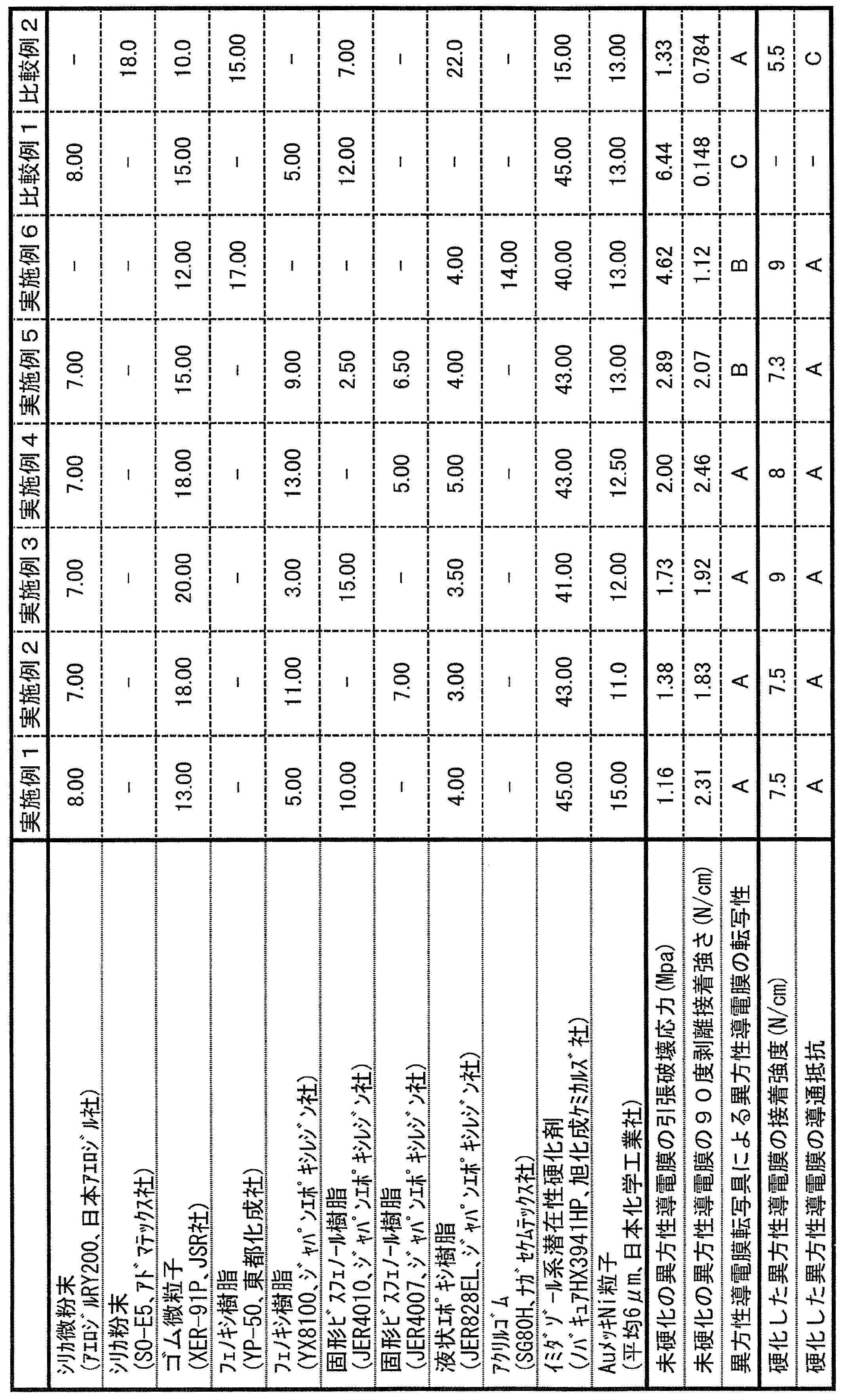
表1から、未硬化の異方性導電膜の引張破壊応力が1.0~2.0MPaの範囲にあり且つ90度剥離接着強さが1.5~2.5N/cmの範囲内にある実施例1~4の異方性導電膜転写具は、手動で異方性導電膜を転写することができる。また、硬化した後の異方性導電膜の接着強度と導通抵抗の特性も好ましいことがわかる。
実施例5及び6については、異方性導電膜を転写するのに十分な接着性が見られたが、実施例1及び2に比べて切断することが困難であり、結果として転写性が若干低下したが実用上問題のないレベルであった。
一方、未硬化の異方性導電膜の引張破壊応力が5.0MPaを超えている比較例1の場合、異方性導電膜の転写性が実施例1~6の場合に比べ大きく低下していることがわかる。なお、比較例1の場合、未硬化の異方性導電膜の90度剥離接着強さが0.148N/cmとなり、1.0N/cmを大きく下回ったために仮貼りそのものが不可能であった。
また、比較例2の場合、未硬化の異方性導電膜の90度剥離接着強さが1.0N/cmを下回っているために、仮貼りは不可能ではなかったものの、硬化後の異方性導電膜の接着強度も7.0N/cmを下回り十分とはいえず、結果的に十分な導通抵抗値を得ることができなかった。
本発明の異方性導電膜転写具においては、異方性導電テープを構成する異方性導電膜の引張破壊応力と接着強さとが所定の範囲に設定されている。このため、本発明の異方性導電膜転写具は、異方性導電テープを、発熱部や電源部が設けられていない転写具を用いて、被転写面に手動で手軽に仮貼りすることができるので、異方性導電テープの手動の転写具として有用である。
Claims (4)
- 基材テープ上に異方性導電膜が仮貼りされている異方性導電テープから該異方性導電膜を被転写面に感圧転写する異方性導電膜転写具であって、
異方性導電テープをその異方性導電膜を外側にして巻き回している巻出リール、
巻出リールから引き出された異方性導電テープを被転写面に押圧し、異方性導電膜を被転写面に転写する転写ヘッド、
異方性導電膜が被転写面に転写した後の基材テープを巻き取る巻取リール、及び
巻出リールと巻取リールとの回転を、異方性導電テープが緩まないように連動させる連動機構を備え、
異方性導電膜の未硬化の状態におけるJIS K7127による引張破壊応力が1.0~5.0MPaであり、且つ異方性導電膜がガラス繊維強化エポキシ板に転写された場合に、未硬化の状態におけるJIS K6854-1によるその90度剥離接着強さが1.0~2.5N/cmである異方性導電膜転写具。 - 連動機構が、巻出リールと同軸に設けた巻出プーリーと、巻取リールと同軸に設けた巻取プーリーと、それらを回動可能に連結するベルトとから構成されている請求項1記載の異方性導電膜転写具。
- 連動機構が、巻出リールに、それと同角速度で回転するように設置された第1平歯車と、巻取リールに、それと同角速度で回転するように設置され、該第1平歯車と噛み合わされ、第1平歯車より歯数の少ない第2平歯車とから構成されている請求項1記載の異方性導電膜転写具。
- 配線基板の接続部に、異方性導電膜を介して電子部品を異方性導電接続する接続方法であって、
配線基板の接続部に対し、請求項1記載の異方性導電膜転写具の転写ヘッドで異方性導電フィルムを基材テープ側から押圧しながら、異方性導電テープが巻出リールから引き出されるように、異方性導電膜転写具を移動させることにより、該接続部に異方性導電層を転写して仮貼りするとともに、異方性導電膜が剥離された基材テープを巻取る工程、及び
配線基板の接続部に仮貼りされた異方性導電膜に対し、電子部品を位置合わせして本熱圧着する工程
を有する接続方法。
Applications Claiming Priority (2)
| Application Number | Priority Date | Filing Date | Title |
|---|---|---|---|
| JP2008-085740 | 2008-03-28 | ||
| JP2008085740A JP5332259B2 (ja) | 2008-03-28 | 2008-03-28 | 異方性導電膜転写具及び接続方法 |
Publications (1)
| Publication Number | Publication Date |
|---|---|
| WO2009118944A1 true WO2009118944A1 (ja) | 2009-10-01 |
Family
ID=41113167
Family Applications (1)
| Application Number | Title | Priority Date | Filing Date |
|---|---|---|---|
| PCT/JP2008/070546 Ceased WO2009118944A1 (ja) | 2008-03-28 | 2008-11-12 | 異方性導電膜転写具及び接続方法 |
Country Status (3)
| Country | Link |
|---|---|
| JP (1) | JP5332259B2 (ja) |
| TW (1) | TW200941507A (ja) |
| WO (1) | WO2009118944A1 (ja) |
Cited By (2)
| Publication number | Priority date | Publication date | Assignee | Title |
|---|---|---|---|---|
| WO2011111784A1 (ja) * | 2010-03-12 | 2011-09-15 | 日立化成工業株式会社 | 接着材リール |
| CN113815339A (zh) * | 2020-06-18 | 2021-12-21 | 国誉株式会社 | 转印用具 |
Families Citing this family (6)
| Publication number | Priority date | Publication date | Assignee | Title |
|---|---|---|---|---|
| CN102574727B (zh) | 2009-10-15 | 2015-06-24 | 旭硝子株式会社 | 有机led元件的散射层用玻璃以及使用该玻璃的有机led元件 |
| JP6125265B2 (ja) * | 2012-05-07 | 2017-05-10 | 日東電工株式会社 | 積層型導電シート、その製造方法、集電体およびバイポーラ電池 |
| JP6520143B2 (ja) * | 2015-01-23 | 2019-05-29 | 大日本印刷株式会社 | 積層体、それを用いた導電性基材の製造方法、電子デバイスの製造方法、および転写具 |
| KR102354454B1 (ko) * | 2015-12-22 | 2022-01-20 | 주식회사 엘지생활건강 | 피부용 필름막 도포 장치 |
| JP6699784B2 (ja) * | 2019-04-26 | 2020-05-27 | 大日本印刷株式会社 | 積層体、それを用いた導電性基材の製造方法、電子デバイスの製造方法、および転写具 |
| JP6849131B2 (ja) * | 2020-04-30 | 2021-03-24 | 大日本印刷株式会社 | 積層体、それを用いた導電性基材の製造方法、電子デバイスの製造方法、および転写具 |
Citations (12)
| Publication number | Priority date | Publication date | Assignee | Title |
|---|---|---|---|---|
| JPH02146092U (ja) * | 1989-05-12 | 1990-12-11 | ||
| JPH051265A (ja) * | 1991-06-24 | 1993-01-08 | Toray Ind Inc | 導電性接着剤 |
| JPH07157740A (ja) * | 1993-12-07 | 1995-06-20 | Nissan Motor Co Ltd | 接着性樹脂組成物 |
| JPH10181985A (ja) * | 1996-12-27 | 1998-07-07 | Kokuyo Co Ltd | 転着テープヘッド |
| JPH1134587A (ja) * | 1997-07-23 | 1999-02-09 | Tombow Pencil Co Ltd | 塗布具 |
| JP2000343890A (ja) * | 1999-06-07 | 2000-12-12 | Fujicopian Co Ltd | 塗膜転写具 |
| JP2001019914A (ja) * | 1999-07-07 | 2001-01-23 | Pilot Corp | 感圧転写テープおよび転写具 |
| JP2001171033A (ja) * | 1999-12-17 | 2001-06-26 | Sony Chem Corp | 多層異方性導電膜積層体 |
| JP2001262078A (ja) * | 2000-03-17 | 2001-09-26 | Sony Chem Corp | 接続材料 |
| JP2004210524A (ja) * | 2003-01-08 | 2004-07-29 | Hitachi Chem Co Ltd | 接着具 |
| JP2004311327A (ja) * | 2003-04-10 | 2004-11-04 | Mitsubishi Plastics Ind Ltd | 導電性基材 |
| JP2006023911A (ja) * | 2004-07-07 | 2006-01-26 | Hitachi Chem Co Ltd | 電子インレット付フィルム、電子インレットカートリッジ及び電子インレットの装着方法 |
-
2008
- 2008-03-28 JP JP2008085740A patent/JP5332259B2/ja active Active
- 2008-11-12 WO PCT/JP2008/070546 patent/WO2009118944A1/ja not_active Ceased
- 2008-11-18 TW TW097144461A patent/TW200941507A/zh unknown
Patent Citations (12)
| Publication number | Priority date | Publication date | Assignee | Title |
|---|---|---|---|---|
| JPH02146092U (ja) * | 1989-05-12 | 1990-12-11 | ||
| JPH051265A (ja) * | 1991-06-24 | 1993-01-08 | Toray Ind Inc | 導電性接着剤 |
| JPH07157740A (ja) * | 1993-12-07 | 1995-06-20 | Nissan Motor Co Ltd | 接着性樹脂組成物 |
| JPH10181985A (ja) * | 1996-12-27 | 1998-07-07 | Kokuyo Co Ltd | 転着テープヘッド |
| JPH1134587A (ja) * | 1997-07-23 | 1999-02-09 | Tombow Pencil Co Ltd | 塗布具 |
| JP2000343890A (ja) * | 1999-06-07 | 2000-12-12 | Fujicopian Co Ltd | 塗膜転写具 |
| JP2001019914A (ja) * | 1999-07-07 | 2001-01-23 | Pilot Corp | 感圧転写テープおよび転写具 |
| JP2001171033A (ja) * | 1999-12-17 | 2001-06-26 | Sony Chem Corp | 多層異方性導電膜積層体 |
| JP2001262078A (ja) * | 2000-03-17 | 2001-09-26 | Sony Chem Corp | 接続材料 |
| JP2004210524A (ja) * | 2003-01-08 | 2004-07-29 | Hitachi Chem Co Ltd | 接着具 |
| JP2004311327A (ja) * | 2003-04-10 | 2004-11-04 | Mitsubishi Plastics Ind Ltd | 導電性基材 |
| JP2006023911A (ja) * | 2004-07-07 | 2006-01-26 | Hitachi Chem Co Ltd | 電子インレット付フィルム、電子インレットカートリッジ及び電子インレットの装着方法 |
Cited By (5)
| Publication number | Priority date | Publication date | Assignee | Title |
|---|---|---|---|---|
| WO2011111784A1 (ja) * | 2010-03-12 | 2011-09-15 | 日立化成工業株式会社 | 接着材リール |
| JPWO2011111784A1 (ja) * | 2010-03-12 | 2013-06-27 | 日立化成株式会社 | 接着材リール |
| JP2015083691A (ja) * | 2010-03-12 | 2015-04-30 | 日立化成株式会社 | 接着材リール |
| CN113815339A (zh) * | 2020-06-18 | 2021-12-21 | 国誉株式会社 | 转印用具 |
| CN113815339B (zh) * | 2020-06-18 | 2024-03-26 | 国誉株式会社 | 转印用具 |
Also Published As
| Publication number | Publication date |
|---|---|
| TW200941507A (en) | 2009-10-01 |
| JP5332259B2 (ja) | 2013-11-06 |
| JP2009238676A (ja) | 2009-10-15 |
Similar Documents
| Publication | Publication Date | Title |
|---|---|---|
| JP5332259B2 (ja) | 異方性導電膜転写具及び接続方法 | |
| TWI356658B (en) | Members for circuit board, method and device for m | |
| JP6036694B2 (ja) | 接着材リール、ブロッキング抑制方法、接着材リールの交換方法、接着材テープの繰出し方法、接着材リールの製造方法、リールキット、及び梱包体 | |
| CN107001868B (zh) | 粘着胶带 | |
| CN106553395B (zh) | 剥离性优异的离型膜 | |
| JPWO2009069661A1 (ja) | 粘着シート、その製造方法、及びその貼合方法 | |
| JP5996241B2 (ja) | 接着フィルムの貼着装置、接着フィルムの貼着方法、及び接続構造体 | |
| JP2008156126A (ja) | 接着剤テープの接続方法及び接着剤テープ接続体 | |
| JP3637350B2 (ja) | 粘着性テ−プ片の貼着装置 | |
| CN103865415A (zh) | 各向异性导电膜及其制造方法、半导体装置及其制造方法 | |
| CN109451675B (zh) | 一种辅料转帖工艺 | |
| TWI679113B (zh) | 表面保護膜以及貼有該膜之光學元件 | |
| CN101580677B (zh) | 能剥离的粘接带 | |
| JP2004202738A (ja) | 接着材テープの接続方法 | |
| KR20050104812A (ko) | 평판표시장치의 제조방법 | |
| JP2025027078A (ja) | ロール体の製造方法およびロール体 | |
| JPH11317173A (ja) | 異方性導電膜の除去方法及び除去装置 | |
| TWI480221B (zh) | 電路連接用膠帶、接著劑捲軸以及電路連接體的製造方法 | |
| JP3503735B2 (ja) | 異方導電性接着フィルム巻重体 | |
| KR100669792B1 (ko) | 가공 기판의 제조방법, 이를 이용한 평판 표시장치의제조방법 및 플렉시블 기판 가접합 장치 | |
| JP6186941B2 (ja) | 接着剤リール | |
| CN104169200B (zh) | 粘接膜的贴附方法和粘接膜贴附装置 | |
| JP2001152105A (ja) | 異方導電性接着フィルム | |
| CN221296773U (zh) | 一种泡棉胶带 | |
| JP2007182534A (ja) | 感圧転写粘着テープおよび塗膜転写具 |
Legal Events
| Date | Code | Title | Description |
|---|---|---|---|
| 121 | Ep: the epo has been informed by wipo that ep was designated in this application |
Ref document number: 08873667 Country of ref document: EP Kind code of ref document: A1 |
|
| DPE1 | Request for preliminary examination filed after expiration of 19th month from priority date (pct application filed from 20040101) | ||
| NENP | Non-entry into the national phase |
Ref country code: DE |
|
| 122 | Ep: pct application non-entry in european phase |
Ref document number: 08873667 Country of ref document: EP Kind code of ref document: A1 |