WO2009113602A1 - 樹脂基板の製造方法および樹脂基板 - Google Patents
樹脂基板の製造方法および樹脂基板 Download PDFInfo
- Publication number
- WO2009113602A1 WO2009113602A1 PCT/JP2009/054715 JP2009054715W WO2009113602A1 WO 2009113602 A1 WO2009113602 A1 WO 2009113602A1 JP 2009054715 W JP2009054715 W JP 2009054715W WO 2009113602 A1 WO2009113602 A1 WO 2009113602A1
- Authority
- WO
- WIPO (PCT)
- Prior art keywords
- resin layer
- resin
- layer
- conductive paste
- substrate
- Prior art date
- Legal status (The legal status is an assumption and is not a legal conclusion. Google has not performed a legal analysis and makes no representation as to the accuracy of the status listed.)
- Ceased
Links
Images






Classifications
-
- H—ELECTRICITY
- H05—ELECTRIC TECHNIQUES NOT OTHERWISE PROVIDED FOR
- H05K—PRINTED CIRCUITS; CASINGS OR CONSTRUCTIONAL DETAILS OF ELECTRIC APPARATUS; MANUFACTURE OF ASSEMBLAGES OF ELECTRICAL COMPONENTS
- H05K3/00—Apparatus or processes for manufacturing printed circuits
- H05K3/40—Forming printed elements for providing electric connections to or between printed circuits
- H05K3/4038—Through-connections; Vertical interconnect access [VIA] connections
- H05K3/4053—Through-connections; Vertical interconnect access [VIA] connections by thick-film techniques
- H05K3/4069—Through-connections; Vertical interconnect access [VIA] connections by thick-film techniques for via connections in organic insulating substrates
-
- H—ELECTRICITY
- H05—ELECTRIC TECHNIQUES NOT OTHERWISE PROVIDED FOR
- H05K—PRINTED CIRCUITS; CASINGS OR CONSTRUCTIONAL DETAILS OF ELECTRIC APPARATUS; MANUFACTURE OF ASSEMBLAGES OF ELECTRICAL COMPONENTS
- H05K1/00—Printed circuits
- H05K1/02—Details
- H05K1/11—Printed elements for providing electric connections to or between printed circuits
- H05K1/111—Pads for surface mounting, e.g. lay-out
- H05K1/112—Pads for surface mounting, e.g. lay-out directly combined with via connections
- H05K1/113—Via provided in pad; Pad over filled via
-
- H—ELECTRICITY
- H05—ELECTRIC TECHNIQUES NOT OTHERWISE PROVIDED FOR
- H05K—PRINTED CIRCUITS; CASINGS OR CONSTRUCTIONAL DETAILS OF ELECTRIC APPARATUS; MANUFACTURE OF ASSEMBLAGES OF ELECTRICAL COMPONENTS
- H05K2201/00—Indexing scheme relating to printed circuits covered by H05K1/00
- H05K2201/03—Conductive materials
- H05K2201/0332—Structure of the conductor
- H05K2201/0335—Layered conductors or foils
- H05K2201/0347—Overplating, e.g. for reinforcing conductors or bumps; Plating over filled vias
-
- H—ELECTRICITY
- H05—ELECTRIC TECHNIQUES NOT OTHERWISE PROVIDED FOR
- H05K—PRINTED CIRCUITS; CASINGS OR CONSTRUCTIONAL DETAILS OF ELECTRIC APPARATUS; MANUFACTURE OF ASSEMBLAGES OF ELECTRICAL COMPONENTS
- H05K2203/00—Indexing scheme relating to apparatus or processes for manufacturing printed circuits covered by H05K3/00
- H05K2203/06—Lamination
- H05K2203/063—Lamination of preperforated insulating layer
-
- H—ELECTRICITY
- H05—ELECTRIC TECHNIQUES NOT OTHERWISE PROVIDED FOR
- H05K—PRINTED CIRCUITS; CASINGS OR CONSTRUCTIONAL DETAILS OF ELECTRIC APPARATUS; MANUFACTURE OF ASSEMBLAGES OF ELECTRICAL COMPONENTS
- H05K3/00—Apparatus or processes for manufacturing printed circuits
- H05K3/46—Manufacturing multilayer circuits
- H05K3/4644—Manufacturing multilayer circuits by building the multilayer layer by layer, i.e. build-up multilayer circuits
- H05K3/4652—Adding a circuit layer by laminating a metal foil or a preformed metal foil pattern
Definitions
- the present invention relates to a method for producing a resin substrate and a resin having at least one resin layer and electrically connecting wiring patterns formed on upper and lower surfaces by a conductive paste filled in a through-hole formed in the resin layer Regarding the substrate.
- this type of resin substrate is formed as follows.
- components such as a semiconductor 601 and a chip component 604 are mounted on a wired transfer plate or a multilayer structure substrate (multilayer printed wiring board, etc.) 600.
- a core layer 605 having a built-in component is formed by being embedded in a sheet-like material 602 made of a mixture of an inorganic filler and an uncured thermosetting resin.
- Reference numeral 603 denotes an interlayer connection conductor formed by filling a through hole with a conductive paste.
- a wiring layer 606 is formed.
- the upper and lower wiring pattern layers are formed with a laser or the like on a sheet-like material composed of a mixture of an inorganic filler and an uncured thermosetting resin or an organic film having adhesive layers formed on both surfaces.
- a through-hole for conducting is formed. Then, the through hole is filled with a conductive paste, and this is used as a wiring layer 606.
- the wiring layer 606 is aligned and overlapped on the upper and lower surfaces of the core layer 605, and a copper foil 608 is further stacked. Then, these layers are superposed and heated and pressed to cure the thermosetting resin of the core layer 605 and the wiring layer 606 and the conductive paste filled in the through holes, whereby the wiring layer is formed on both surfaces of the core layer 605. Form.
- a wiring pattern 609 is formed by subjecting the copper foil 608 to a chemical etching method.
- a resin substrate is formed in which the wiring pattern layers on the upper and lower surfaces of the core layer are electrically connected.
- the conductive paste is filled in the through holes, and then the uncured wiring layer and the core layer 605 containing the components are overlaid and heated and pressed.
- the conductive paste filled in the through hole may wrap around the interface between the core layer 605 and the wiring layer 606 when the layer is pressed.
- a short circuit occurs between the wiring pattern on the surface of the core layer 605 and the adjacent interlayer connection conductors due to the conductive paste that wraps around, causing a conduction abnormality.
- the distance between wiring patterns tends to be closer, and the inflow phenomenon of the conductive paste as described above may hinder improvement in reliability.
- an object of the present invention is to provide a highly reliable resin substrate that can prevent a short circuit due to the inflow of conductive paste even when the distance between wiring patterns is close.
- a resin substrate manufacturing method includes a first step of preparing a substrate body having a via land on an upper surface, and a resin layer in which a through hole is formed at a position corresponding to the via land. A second step of forming a conductive paste on the substrate body, a third step of filling the through hole with a conductive paste, and forming a wiring pattern electrically connected to the conductive paste on the resin layer. And a fourth step. (Claim 1).
- the metal foil is pressure-bonded to the uncured resin layer to cure the resin layer, and the metal foil is processed.
- the method further includes a step of forming the wiring pattern.
- the resin layer is irradiated with laser from the resin layer side to the uncured resin layer on which a metal foil is pasted.
- the fourth step includes a step of forming a conductive layer covering the conductive paste on the metal foil, and the metal foil and the conductive layer. And a step of simultaneously processing (claim 4).
- the third step is characterized in that the conductive paste is filled by printing (claim 5).
- or 5 is equipped with the process of hardening the said resin layer and the said electrically conductive paste simultaneously after a said 3rd process (Claim). 6).
- the resin substrate according to the present invention includes a substrate body having via lands on the upper surface, a resin layer formed on the substrate body, and a metal pasted on the uncured resin layer.
- the resin substrate according to claim 7 may be formed by simultaneously processing a conductive layer formed by coating the conductive paste on the metal foil and the metal foil instead of the wiring pattern.
- a wiring pattern electrically connected to the paste is provided (claim 8).
- the conductive paste is filled into the through hole of the resin layer, so that the substrate body and the resin layer are in close contact with each other, and then the through hole is filled. It is possible to prevent the conductive paste from flowing into the interface between the substrate body and the resin layer. Accordingly, a short circuit of the wiring pattern due to the conductive paste flowing into the interface between the substrate body and the resin layer does not occur as in the prior art, and a highly reliable resin substrate can be obtained.
- the metal foil is pressure-bonded to the resin layer, it is possible to form the wiring pattern more easily than forming the wiring pattern by forming a plating layer on the resin layer. Further, since the metal foil is pressure-bonded to the uncured resin layer, the metal foil is bonded to the resin layer simultaneously with the curing of the resin layer. Therefore, a wiring pattern can be formed by patterning the metal foil adhered to the resin layer. Therefore, the process of forming the wiring pattern can be simplified and the manufacturing cost can be reduced.
- the conductive paste filled in the through hole of the resin layer is covered with the conductive layer, the conductive paste and the conductive layer are accurately conducted to form a more reliable wiring pattern. can do.
- the side surface of the conductive paste can be covered with the metal foil, the contact area between the conductive paste and the wiring pattern can be increased, and the conduction resistance can be reduced.
- the conductive paste when the conductive paste is filled by printing, the conductive paste is filled in the through hole by horizontally moving while pressing the squeegee on the resin layer. Can be filled without gaps.
- the squeegee moves horizontally on the metal foil, so that the resin layer can be prevented from being deformed in the squeegee moving direction by the pressure of the squeegee.
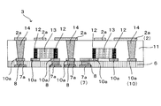
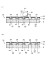
- FIGS. 1 is a cross-sectional view of a resin substrate in the first embodiment
- FIG. 2 is a cross-sectional view of a substrate body in the resin substrate
- FIGS. 3 to 6 are explanatory views of a manufacturing process of the resin substrate.
- the resin substrate 1 in the present embodiment is formed by a substrate body 3 having a wiring pattern 2 including a plurality of via lands 2a on an upper surface, a resin layer 4, and a wiring pattern 5 including a plurality of via lands 5a. Has been.
- the substrate body 3 has a structure in which the first layer 6 and the second layer 11 are stacked and integrated.
- the first layer 6 is made of resin, the first wiring layer 7 including a plurality of via lands 7a is formed, and the first interlayer connection conductor 8 electrically connected to the predetermined via land 7a is formed. Is formed.
- the interlayer connection conductor 8 may be a via conductor or a through conductor.
- a second wiring layer 10 including a plurality of via lands 10 a is formed on the upper surface of the first layer 6 and connected to the first interlayer connection conductor 8. Furthermore, a second layer 11 made of resin is disposed on the upper surface of the second wiring layer 10.
- a component 13 including an electrode 12 is embedded and connected to a land 10 a formed at a position corresponding to the electrode 12.
- a second interlayer connection conductor 14 electrically connected to the second wiring layer 10 is also formed.
- the second interlayer connection conductor 14 may also be a via conductor or a through conductor.
- a wiring pattern 2 including a plurality of via lands 2 a is formed on the upper surface of the second layer 11, and the wiring pattern 2 is connected to the second interlayer connection conductor 14.
- the first wiring layer 7 and the wiring pattern 2 are connected via the first interlayer connection conductor 8, the second wiring layer 10, and the second interlayer connection conductor 14, and the first wiring layer 7 and the electrode 12 of the component 13. Are connected via the first interlayer connection conductor 8 and the second wiring layer 10.
- the wiring pattern 2 in FIG. 2 corresponds to the wiring pattern layer 2 formed on the upper surface of the substrate body 3 in FIG.
- the first interlayer connection conductor 8 and the second interlayer connection conductor 14 are filled with conductive paste, respectively. Accordingly, the first wiring layer 7, the second wiring layer 10, the wiring pattern 2, and the components 13 embedded in the second wiring layer 10 and the second layer 11 are electrically connected to each other.
- the first layer 6 and the second layer 11 are formed of a thermosetting resin such as an epoxy resin in consideration of the ease of the curing process. Moreover, you may form with the photocurable resin hardened
- the substrate body 3 is not limited to the above structure, and may be a ceramic substrate, a transfer plate made of SUS or the like, another component built-in substrate, a via conductor built-in substrate, or the like as long as it has a wiring pattern on the upper surface.
- a multilayer substrate in which these substrates are stacked in combination may be used.
- a resin layer 4 is formed on the upper surface of the substrate body 3.
- the resin layer 4 is formed of, for example, an epoxy thermosetting resin or a mixture of a thermosetting resin and an inorganic filler in consideration of the ease of the curing process.
- a via conductor 15 is formed in the resin layer 4.
- the via conductor 15 is formed by filling a via conductor hole with a conductive paste, and is electrically connected to a predetermined via land 2 a among a plurality of via lands 2 a formed on the upper surface of the substrate body 3.
- a wiring pattern 5 including a plurality of via lands 5 a is formed on the upper surface of the resin layer 4 and is electrically connected to the via conductor 15. Therefore, the wiring pattern 2 and the wiring pattern 5 are electrically connected via the via conductor 15.
- the thickness of the resin layer 4 on which the wiring pattern 5 is formed is, for example, 20 to 50 ⁇ m.
- the resin layer 4 which consists of a mixture of an epoxy-type thermosetting resin and an inorganic filler is formed in the sheet form in the uncured state on the single side
- a carbon dioxide laser is irradiated from the PET film 17 side to form a via conductor hole 18 at a desired position, thereby forming a resin sheet 16.
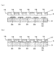
- the resin sheet 16 and the substrate body 3 are integrated. As shown in FIG. 4A, alignment is performed so that the via conductor hole 18 formed in the resin sheet 16 corresponds to the position of the predetermined via land 2 a of the wiring pattern 2 on the upper surface of the substrate body 3. Then, as shown in FIG. 5B, the resin layer 4 of the resin sheet 16 is brought into contact with the upper surface of the substrate body 3 and heated and pressurized at 50 to 130 ° C., and the substrate body 3 and the resin layer 4 are temporarily bonded. And integrate. At this time, since the resin layer 4 is uncured, the via land 2a formed on the upper surface of the substrate body 3 is embedded in the resin layer 4 as shown in FIG. Further, the PET film 17 is positioned on the upper surface of the integrated substrate body 3 and the resin sheet 16.
- the via conductor hole 18 is filled with the conductive paste 20 to form the via conductor 15.
- the conductive paste 20 is filled by a screen printing method.
- the conductive paste 20 is specifically a resin paste mixed with a conductive material (metal).
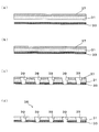
- the squeegee 21 is moved in the horizontal direction (in the direction of the arrow in FIG. 5A) on the upper surface of the PET film 17 of the resin sheet 16 to the via conductor hole 18.
- the conductive paste 20 is filled. Since the conductive paste 20 is filled while pressing the resin sheet 16 with the squeegee 21, the via conductor hole 18 is filled with the conductive paste 20 without any gap.
- a wiring pattern 5 is formed on the upper surface of the resin layer 4.
- the copper foil 23 is brought into contact with the upper surface of the resin layer 4 and pressed.
- the roughened surface of the copper foil 23 is disposed opposite to the resin layer 4, and the resin layer 4 and the copper foil 23 are brought into contact with each other.
- the resin layer 4 and the substrate body 3 to which the copper foil 23 is bonded are heated at 180 to 200 ° C.
- the conductive paste 20 filled in the resin layer 4 and the via conductor hole 18 is cured.
- the copper foil 23 that is pressure-bonded to the resin layer 4 is also bonded to the resin layer 4 at the same time.
- the copper foil 23 has a thickness of about 12 ⁇ m, for example, but the thickness may be changed as appropriate.
- the wiring pattern 5 including the plurality of via lands 5a is formed by processing the copper foil 23 into a pattern by, for example, photolithography and etching.
- the conductive paste 20 is temporarily cured (heated to 100 ° C.) and then protruded from the resin layer 4 before the copper foil 23 is pressure-bonded to the resin layer 4.
- the conductive paste 20 may be polished and then the copper foil may be pressure bonded.
- the wiring pattern 5 is not limited to the copper foil 23 as described above, and a copper alloy or other metal foil may be formed and processed into a pattern. It is also possible to press-bond a copper foil patterned in advance to the upper surface of the resin layer 4. Alternatively, instead of metal foil, a conductive layer made of copper, copper alloy or other conductive metal is formed on the entire upper surface of the resin layer 4 by electrolytic plating or electroless plating, and the conductive layer is processed into a pattern. Can do.
- the conductive paste 20 is filled in the via conductor holes 18 of the resin sheet 16. 4 and the conductive paste 20 can be prevented from flowing into the interface between the substrate body 3 and the resin layer 4. Therefore, a short circuit of the wiring pattern due to the conductive paste 20 flowing into the interface between the substrate body 3 and the resin layer 4 does not occur as in the conventional case, and the resin substrate 1 having excellent reliability can be obtained. .
- the copper foil 23 is formed on the upper surface of the resin layer 4 by crimping and processed into the wiring pattern 5
- a conductive layer by plating is formed on the upper surface of the resin layer 4 and processed into the wiring pattern. It is possible to form a wiring pattern more easily than this.
- the copper foil 23 is pressure-bonded to the uncured resin layer 4, the copper foil 23 is bonded to the resin layer 4 simultaneously with the curing of the resin layer 4 and the conductive paste 20. Therefore, the process can be simplified and the manufacturing cost can be reduced.
- FIG. 7 is a cross-sectional view of a resin substrate in the second embodiment
- FIGS. 8 and 11 are explanatory views of the manufacturing process.
- the resin substrate 30 of the present embodiment includes the substrate body 3 having the wiring pattern 2 including the via land 2a on the upper surface, like the resin substrate 1 in the first embodiment. Since the configuration of the substrate body 3 is the same as that of the first embodiment, description thereof is omitted.
- a resin layer 31 is formed on the upper surface of the substrate body 3.
- a via conductor 32 electrically connected to a predetermined via land 2 a among the plurality of via lands 2 a formed on the upper surface of the substrate body 3 is formed in the resin layer 31.
- a copper foil 33 and a conductive layer 34 are formed on the upper surface of the resin layer 31.
- the conductive layer 34 is formed by coating the via conductor 32 and the copper foil 33 by electrolytic plating or electroless plating with copper or a copper alloy or other conductive metal. Then, the copper foil 33 and the conductive layer 34 are simultaneously processed into a pattern to form a wiring pattern layer 35. Therefore, the wiring pattern 2, the via conductor 32, and the wiring pattern layer 35 are electrically connected.
- the resin layer 31 which consists of a mixture of an epoxy-type thermosetting resin and an inorganic filler is formed in the sheet form in the uncured state on the single side
- the copper foil 33 is temporarily crimped
- the roughened surface of the copper foil 33 is disposed opposite to the resin layer 31 so that the resin layer 31 and the copper foil 33 are in contact with each other. Since the temporary pressure bonding is performed at a temperature of about 40 to 60 ° C., the resin layer 31 maintains an uncured state.
- a copper foil having a thickness of about 12 ⁇ m is used, but the thickness may be changed as appropriate.
- a carbon dioxide laser is irradiated to a desired position on the upper surface of the PET film 37 to form a via conductor hole 39.
- the laser beam is reflected on the metal surface, it is difficult to form the via conductor hole in the copper foil 33 by the laser beam.
- the carbon dioxide laser is irradiated from the upper surface of the PET film 37, the resin layer 31 and the copper are formed. Since heat due to laser light is stored at the interface of the foil 33, the via foil 39 can be formed by penetrating through the copper foil 33 simultaneously with the PET film 37 and the resin layer 31 by the heat.
- the via conductor hole 39 is affected by the reflection of the laser light as the resin layer 31 becomes thicker, and as it goes from the PET film 37 side to the copper foil 33 side.
- the hole diameter is small and formed in a taper shape.
- the laser is not limited to a carbon dioxide laser, and may be other lasers.
- the PET film 37 is peeled off, and the resin layer 31 and the copper foil 38 in which the via conductor holes 39 are formed are used as a sheet 36.
- the sheet 36 and the substrate body 3 are integrated. As shown in FIG. 9A, the upper surface of the substrate body 3 having the via land 2 a and the resin layer 31 side of the sheet 36 are arranged to face each other, and the via conductor hole 39 formed in the sheet 36 has the upper surface of the substrate body 3.
- the wiring pattern 2 is aligned so as to correspond to the position of a predetermined via land 2a.
- the resin layer 31 is brought into contact with the upper surface of the substrate body 3 and heated and pressurized at 70 to 130 ° C. to press-bond the substrate body 3 and the resin layer 31.
- the via land 2 a formed on the upper surface of the substrate body 3 is embedded in the resin layer 31 as shown in FIG.
- the copper foil 33 is located on the upper surface of the integrated substrate body 3 and the resin layer 31.
- the via conductor hole 39 is filled with the conductive paste 20, and the via conductor 32 is formed.
- the filling of the conductive paste 20 is performed by the screen printing method as in the first embodiment.
- the conductive paste 20 is specifically a resin paste mixed with a conductive material (metal).
- the filling of the conductive paste 20 by the screen printing method generally moves the squeegee horizontally while pressing the upper surface of the layer having the through-hole. Therefore, when the rigidity of the upper surface is low, The shape may be deformed.
- the shape of the via conductor 15 may be deformed.
- the copper foil 33 since the copper foil 33 is located on the upper surface of the resin layer 31 as described above, as shown in FIG. Even if it moves in the direction of the arrow 10 (a), since the copper foil 33 has higher rigidity than the PET film 17 of the first embodiment, the copper foil 33 does not shift in the direction of the squeegee 21.
- the via conductor 32 is not deformed in the moving direction of the squeegee 21, and from the position of the corresponding via land 2a. There is no significant shift. Therefore, the via conductor 32 with excellent positional accuracy can be formed.
- the sheet 36 and the substrate body 3 are heated at 180 to 200 ° C. Accordingly, the resin layer 31 and the conductive paste 20 are cured, and the copper foil 33 temporarily bonded to the resin layer 31 is also bonded to the resin layer 31 at the same time.
- the upper surface of the copper foil 33 is polished to flatten the via conductor 32 and the copper foil 33.
- a conductive layer 34 is formed on the upper surface of the copper foil 33.
- the conductive layer 34 is formed by covering the via conductor 32 and the copper foil 33 by electrolytic plating or electroless plating with copper or a copper alloy or other conductive metal.
- each via land 35a includes a via land 33a obtained by processing the copper foil 33 and a via land 34a obtained by processing the conductive layer 34.
- the wiring pattern 2, the via conductor 32, and the wiring pattern layer 35 are electrically connected.
- the upper surface and the side surface of the via conductor 32 are covered with the via land 34a processed with the conductive layer 34 and the via land 33a processed with the copper foil 33, respectively.
- the filled conductive paste 20 is not exposed, and the conductive paste 20 and the conductive layer 34 are in direct contact with each other to conduct accurately. Further, since the contact area between the via conductor 32 and the wiring pattern layer 35 is large, the conduction resistance is reduced.
- the copper foil 33 described above is not limited to a copper foil, but may be a copper alloy or other metal foil.
- the conductive paste 20 is filled in the via conductor hole 39 of the sheet 36 after the sheet 36 is pressure-bonded onto the substrate body 3, and thus the substrate body 3, the resin layer 31, and the like. And the conductive paste 20 can be prevented from flowing into the interface between the substrate body 3 and the resin layer 31. Therefore, unlike the conventional case, a short circuit of the wiring pattern due to the conductive paste 20 flowing into the interface between the substrate body 3 and the resin layer 31 does not occur, and a more reliable resin substrate can be obtained. .
- the via paste 39 is filled with the conductive paste 20. Due to the rigidity of 33, deformation of the via conductor 32 when the conductive paste 20 is filled can be prevented. Therefore, the positional accuracy of the via land 2a, the via conductor 32, and the via land 35a can be improved.
- the via conductor 32 is covered with the conductive layer 34, the via conductor 32 and the conductive layer 34 are accurately conducted, and a more reliable wiring pattern can be formed. Moreover, since the side surface of the via conductor 32 is covered with the copper foil 33, the contact area between the via conductor 32 and the wiring pattern layer 35 increases, and the conduction resistance can be reduced. Therefore, it is possible to provide a resin substrate with higher reliability.
- the via conductor holes 18 and 39 are filled with the conductive paste 20 by the screen printing method, but other methods may be used.
- the through hole is formed by irradiation with the carbon dioxide laser, but other lasers may be used. Moreover, you may form a through-hole not only by laser irradiation but by the other method.
- the configurations and materials of the substrate body 3, the resin layers 4 and 31, the copper foils 23 and 33, the conductive layer 34, and the conductive paste 20 are not limited to those described in the above-described embodiments, and their shapes and dimensions Etc. may be anything.
- the present invention relates to a method for producing a resin substrate and a resin having at least one resin layer and electrically connecting wiring patterns formed on upper and lower surfaces by a conductive paste filled in a through-hole formed in the resin layer
- the resin substrate may be applied to a substrate, and the resin substrate may be a substrate having a plurality of resin layers or a component built-in substrate in which components are incorporated in the resin layer.
Landscapes
- Engineering & Computer Science (AREA)
- Microelectronics & Electronic Packaging (AREA)
- Manufacturing & Machinery (AREA)
- Production Of Multi-Layered Print Wiring Board (AREA)
- Printing Elements For Providing Electric Connections Between Printed Circuits (AREA)
Abstract
基板体と配線層の間に導電性ペーストが流入することにより配線パターンの短絡等が起こるのを防止し、信頼性の高い樹脂基板を提供する。
銅箔33を貼設した樹脂層31に、ビア導体用孔39を形成する。そして、上面にビアランド2aを有する基板体3上に樹脂層31を圧着する。その後、ビア導体用孔39に導電性ペーストを充填してビア導体32を形成する。そして、銅箔33と銅箔33上に形成した導電層34をパターンに加工して、ビアランド35aを有する配線パターン層35を形成する。
Description
本発明は、少なくとも一層の樹脂層を有し、樹脂層に形成された貫通孔に充填された導電性ペーストにより上下両面に形成された配線パターンを電気的に接続した樹脂基板の製造方法および樹脂基板に関する。
近年、電子機器の小型化、高性能化に伴い、コンデンサ、チップ抵抗、チップコイル、ICなどの電子部品を高密度、高機能に内蔵した部品内蔵基板や、樹脂層および配線層を複数重ねて形成された樹脂基板が種々提案されている。
この種の樹脂基板は、例えば特許文献1に示す発明では、以下のようにして形成される。
はじめに、図12(a)および(b)に示すように、配線済みの転写板、若しくは多層構造基板(多層プリント配線板など)600に半導体601、チップ部品604等の部品を搭載し、それを同図(c)ないし(e)に示すように、無機質フィラーと未硬化の熱硬化性樹脂の混合物のシート状物602に埋め込んで一体化して部品を内蔵したコア層605を形成する。なお603は、貫通孔に導電性ペーストが充填してなる層間接続導体である。
つぎに、配線層606を形成する。図12(f)に示すように、無機質フィラーと未硬化状態の熱硬化性樹脂の混合物からなるシート状物または両面に接着層を形成した有機フィルムに、レーザー等で上下面の配線パターン層を導通するための貫通孔を形成する。そして、前記貫通孔に導電性ペーストを充填し、これを配線層606とする。
つぎに、図12(f)および(g)に示すように、コア層605の上下面に前記配線層606を位置合わせして重ね、さらに銅箔608を重ねる。そして、これらの層を重ね合わせて加熱、加圧し、コア層605、配線層606の熱硬化性樹脂および貫通孔に充填された導電性ペーストを硬化することで、コア層605の両面に配線層を形成する。
その後、図12(h)に示すように、前記銅箔608に化学エッチング法を施すことによって配線パターン609を形成する。このようにして、コア層の上下面の配線パターン層が電気的に接続された樹脂基板を形成している。
特開2002-261449号公報(段落0055~0059、図6等)
前記特許文献1の方法により配線層606を形成すると、貫通孔に導電性ペーストを充填した後、未硬化の配線層と部品が内蔵されたコア層605を重ね合わせて加熱および加圧するため、これらの層の圧着時に、貫通孔に充填された導電性ペーストがコア層605と配線層606の界面に回り込む可能性がある。その結果、回り込んだ導電性ペーストによりコア層605表面の配線パターンや隣接する層間接続導体の間で短絡が起こり、導通異常を発生する。近年のモジュールの小型化および高機能化が進む中では、配線パターン間の距離は近接する傾向にあるため、上記のような導電性ペーストの流入現象は信頼性向上の妨げになるおそれがある。
したがって、本発明は、配線パターン間の距離が近接している場合でも、導電性ペーストの流入による短絡等を防止でき、信頼性の高い樹脂基板を提供することを目的とする。
上記した目的を達成するために、本発明における樹脂基板の製造方法は、上面にビアランドを有する基板体を用意する第1の工程と、前記ビアランドと対応する位置に貫通孔が形成された樹脂層を前記基板体上に形成する第2の工程と、前記貫通孔に導電性ペーストを充填する第3の工程と、前記樹脂層上面に前記導電性ペーストと電気的に接続された配線パターンを形成する第4の工程とを備えることを特徴としている(請求項1)。
また、請求項1に記載の樹脂基板の製造方法は、前記第4の工程が、未硬化状態の前記樹脂層に金属箔を圧着して前記樹脂層を硬化し、前記金属箔を加工することにより前記配線パターンを形成する工程を含むことを特徴としている(請求項2)。
また、請求項1に記載の樹脂基板の製造方法は、前記第2の工程が、金属箔が貼設された未硬化状態の前記樹脂層に、前記樹脂層側からレーザーを照射して前記樹脂層および前記金属箔を貫通する前記貫通孔を形成した後、前記樹脂層と前記基板体とが対向するように前記樹脂層を前記基板体上に圧着する工程を含み、前記第4の工程は、前記金属箔を加工して前記配線パターンを形成する工程を含むことを特徴としている(請求項3)。
また、請求項3に記載の樹脂基板の製造方法は、前記第4の工程が、前記金属箔上に前記導電性ペーストを被覆する導電層を形成する工程と、前記金属箔と前記導電層を同時に加工する工程とを含むことを特徴としている(請求項4)。
また、請求項1ないし請求項4に記載の樹脂基板の製造方法は、前記第3の工程が、前記導電性ペーストを印刷により充填することを特徴としている(請求項5)。
また、請求項1ないし請求項5に記載の樹脂基板の製造方法は、前記第3の工程の後に、前記樹脂層と前記導電性ペーストを同時に硬化する工程を備えることを特徴としている(請求項6)。
上記した目的を達成するために、本発明における樹脂基板は、上面にビアランドを有する基板体と、前記基板体上に形成された樹脂層と、未硬化状態の前記樹脂層に貼設された金属箔と、前記樹脂層側からレーザーを照射することにより前記ビアランドと対応する位置の前記樹脂層および前記金属箔を貫通して形成された貫通孔と、前記貫通孔に充填された導電性ペーストと、前記樹脂層上面の、前記金属箔を加工して形成され前記導電性ペーストと電気的に接続された配線パターンとを備えることを特徴としている(請求項7)。
また、請求項7に記載の樹脂基板は、前記配線パターンに代えて、前記金属箔上に前記導電性ペーストを被覆して形成された導電層と前記金属箔とを同時に加工して前記導電性ペーストと電気的に接続された配線パターンを備えることを特徴としている(請求項8)。
請求項1の発明によれば、基板体上に樹脂層を形成した後、樹脂層の貫通孔に導電性ペーストを充填するので、基板体と樹脂層とが密着し、その後に貫通孔に充填された導電性ペーストが基板体と樹脂層との界面に流入するのを防止することができる。したがって、従来のように基板体と樹脂層との界面に導電性ペーストが流入することによる配線パターンの短絡が発生することはなく、信頼性の優れた樹脂基板を得ることができる。
請求項2の発明によれば、金属箔を樹脂層に圧着するため、樹脂層にめっき層を形成して配線パターンを形成するよりも簡便に配線パターンを形成することができる。また、未硬化の樹脂層に金属箔を圧着するため、樹脂層の硬化と同時に金属箔も樹脂層に接着される。よって、樹脂層に接着された金属箔をパターニングすることにより配線パターンを形成することができる。したがって、配線パターンを形成する工程を簡素化でき、製造コストの低減を図ることも可能になる。
請求項3の発明によれば、金属箔が貼設された状態の樹脂層に貫通孔を形成した後、貫通孔に導電性ペーストを充填するため、金属箔によって樹脂層の変形を防止しつつ貫通孔に導電性ペーストを充填することができる。したがって、配線パターンの短絡が発生しないだけでなく、ビアランドと貫通孔、および、貫通孔と配線パターンの位置精度を向上させることができる。
請求項4の発明によれば、樹脂層の貫通孔に充填された導電性ペーストを導電層により被覆するため、導電性ペーストと導電層が精度よく導通し、より信頼性の高い配線パターンを形成することができる。また、導電性ペーストの側面まで金属箔により覆うことができ、導電性ペーストと配線パターンとの接触面積が増加し、導通抵抗を低減することができる。
請求項5の発明によれば、印刷により導電性ペーストを充填する際、樹脂層上にスキージを圧接しながら水平移動させて導電性ペーストを貫通孔に充填するため、貫通孔に導電性ペーストを隙間なく充填することができる。また、樹脂層上に金属箔を貼設している場合には、金属箔上をスキージが水平移動するため、樹脂層がスキージの圧力によってスキージの移動方向に変形することを防止できる。
請求項6の発明によれば、樹脂層および導電性ペーストの硬化工程を一つにまとめることができるため、樹脂基板の製造工程を簡素化することが可能である。
請求項7および8の発明によれば、請求項3および4の発明それぞれと同様の効果を奏する新規な樹脂基板を提供することができる。
1……樹脂基板
2……配線パターン層
2a……ビアランド
3……基板体
4……樹脂層
5……配線パターン
5a……ビアランド
15……ビア導体
18……ビア導体用孔
20……導電性ペースト
23……銅箔(金属箔)
30……樹脂基板
31……樹脂層
32……ビア導体
33……銅箔(金属箔)
35……配線パターン層
35a……ビアランド
39……ビア導体用孔
2……配線パターン層
2a……ビアランド
3……基板体
4……樹脂層
5……配線パターン
5a……ビアランド
15……ビア導体
18……ビア導体用孔
20……導電性ペースト
23……銅箔(金属箔)
30……樹脂基板
31……樹脂層
32……ビア導体
33……銅箔(金属箔)
35……配線パターン層
35a……ビアランド
39……ビア導体用孔
(第1実施形態)
請求項1、2、5、6に対応する第1実施形態について、図1ないし図6を参照して説明する。なお、図1は第1実施形態における樹脂基板の断面図、図2は樹脂基板における基板体の断面図、図3ないし図6は樹脂基板の製造工程の説明図である。
請求項1、2、5、6に対応する第1実施形態について、図1ないし図6を参照して説明する。なお、図1は第1実施形態における樹脂基板の断面図、図2は樹脂基板における基板体の断面図、図3ないし図6は樹脂基板の製造工程の説明図である。
本実施形態における樹脂基板1は、図1に示すように、上面に複数のビアランド2aを含む配線パターン2を有する基板体3と、樹脂層4と、複数のビアランド5aを含む配線パターン5によって形成されている。
基板体3は図2に示すように、第一層6、第二層11を重ねて一体化した構造である。
図2に示すように、第一層6は樹脂からなり、複数のビアランド7aを含む第一配線層7が形成され、所定のビアランド7aと電気的に接続された第一層間接続導体8が形成されている。この層間接続導体8はビア導体であってもスルー導体であってもよい。
第一層6の上面には、複数のビアランド10aを含む第二配線層10が形成され、第一層間接続導体8と接続されている。さらに、第二配線層10の上面には、樹脂からなる第二層11が配設されている。
第二層11には、電極12を備えた部品13が埋設され、電極12に対応する位置に形成されたランド10aと接続されている。また、第二配線層10と電気的に接続された第二層間接続導体14が形成されている。この第二層間接続導体14もビア導体であってもスルー導体であってもよい。
第二層11の上面には、複数のビアランド2aを含む配線パターン2が形成され、配線パターン2は第二層間接続導体14と接続されている。
すなわち、第一配線層7と配線パターン2とは第一層間接続導体8、第二配線層10、第二層間接続導体14を介して接続され、第一配線層7と部品13の電極12とは第一層間接続導体8および第二配線層10を介して接続されている。ここで、図2における配線パターン2が、図1における基板体3の上面に形成された配線パターン層2に相当する。
また前記第一層間接続導体8、第二層間接続導体14には、導電性ペーストがそれぞれ充填されている。よって、第一配線層7と第二配線層10と配線パターン2、および第二配線層10と第二層11に埋設される部品13は、それぞれ電気的に接続されている。
なお、第一層6、第二層11は、硬化処理の容易さなどを考慮して、例えばエポキシ系樹脂等の熱硬化性樹脂により形成されている。また、これ以外にも紫外線により硬化する光硬化性樹脂により形成してもよい。ただし、硬化による収縮率の低いものを選定するのがよい。
また、基板体3は、上記のような構造に限らず、上面に配線パターンを有するものであれば、セラミック基板、SUSなどからなる転写板、その他の部品内蔵基板やビア導体内蔵基板等であってもよいし、これらの基板を組み合わせて重ねた多層基板であってもよい。
また、図1に示すように、基板体3の上面には樹脂層4が形成されている。樹脂層4は、硬化処理の容易さ等を考慮して、例えばエポキシ系熱硬化樹脂や、熱硬化性樹脂と無機フィラーの混合物等により形成される。そして、樹脂層4にはビア導体15が形成されている。ビア導体15は、ビア導体用孔に導電性ペーストを充填してなり、基板体3上面に形成された複数のビアランド2aのうち、所定のビアランド2aと電気的に接続されている。
さらに、樹脂層4の上面には、複数のビアランド5aを含む配線パターン5が形成され、ビア導体15と電気的に接続されている。したがって、配線パターン2と配線パターン5はビア導体15を介して電気的に接続されている。配線パターン5が形成された樹脂層4の厚さは、例えば20~50μmである。
次に、樹脂基板1の製造方法について、図3ないし図6を参照して以下に説明する。
まず樹脂シート16の製造方法について説明する。図3(a)に示すように、可撓性を有するPETフィルム17の片面に、エポキシ系熱硬化性樹脂と無機フィラーの混合物からなる樹脂層4を、未硬化状態でシート状に形成する。そして、同図(b)に示すように、PETフィルム17側から炭酸ガスレーザを照射して、所望の位置にビア導体用孔18を形成し、樹脂シート16を形成する。
次に、上記した樹脂シート16と基板体3を一体化する。図4(a)に示すように、樹脂シート16に形成されたビア導体用孔18が、基板体3上面の配線パターン2の所定のビアランド2aの位置に対応するように位置合わせを行う。そして、同図(b)に示すように、樹脂シート16の樹脂層4を基板体3の上面に当接して50~130℃で加熱、加圧し、基板体3と樹脂層4を仮圧着して一体化する。このとき、樹脂層4は未硬化であるため、同図(b)に示すように、基板体3の上面に形成されたビアランド2aは樹脂層4に埋設される。また、一体化した基板体3と樹脂シート16の上面には、PETフィルム17が位置することとなる。
次に、ビア導体用孔18に導電性ペースト20を充填し、ビア導体15を形成する。導電性ペースト20の充填は、スクリーン印刷方法により行う。なお、導電性ペースト20は、具体的には導電材料(金属)を混入した樹脂ペーストである。
図5(a)、(b)に示すように、スキージ21を樹脂シート16のPETフィルム17の上面に水平方向(図5(a)中の矢印方向)に移動させながらビア導体用孔18に導電性ペースト20を充填する。スキージ21により樹脂シート16を加圧しながら導電性ペースト20を充填するため、ビア導体用孔18には隙間なく導電性ペースト20が充填される。
その後、図5(c)に示すように、樹脂シート16からPETフィルム17を剥離する。
次に、樹脂層4の上面に配線パターン5を形成する。まず、図6(a)に示すように、樹脂層4の上面に銅箔23を当接して圧着する。このとき、樹脂層4と銅箔23の密着性を良好にするために、銅箔23の粗化面を樹脂層4と対向配置して、樹脂層4と銅箔23を当接する。そして、銅箔23を圧着した樹脂層4および基板体3を180~200℃で加熱する。これにより、樹脂層4とビア導体用孔18に充填された導電性ペースト20が硬化される。また、樹脂層4に圧着された銅箔23も同時に樹脂層4に接着される。なお、銅箔23は、例えば約12μmの厚さのものを使用するが、その厚さは適宜変更してもよい。
その後、図6(b)に示すように、銅箔23を例えばフォトリソグラフィ、エッチングによりパターンに加工することにより、複数のビアランド5aを含む配線パターン5を形成する。
また、導電性ペースト20をビア導体用孔18に充填後、銅箔23を樹脂層4に圧着する前に導電性ペースト20のみを仮硬化させ(100℃に加熱)、樹脂層4から突出した導電性ペースト20を研磨し、その後銅箔を圧着してもよい。
また、配線パターン5は上記したような銅箔23に限らず、銅合金その他の金属箔を形成してパターンに加工してもよい。また、予めパターン化された銅箔を樹脂層4の上面に圧着することも可能である。また、金属箔に代えて、樹脂層4の上面全面に電解めっき、無電解めっきにより銅又は銅合金その他の導電性金属からなる導電層を形成し、導電層をパターンに加工することによっても形成し得る。
以上のように第1実施形態によれば、基板体3上に樹脂シート16を圧着した後、樹脂シート16のビア導体用孔18に導電性ペースト20を充填するので、基板体3と樹脂層4とが密着し、導電性ペースト20が基板体3と樹脂層4との界面に流入するのを防止することができる。したがって、従来のように基板体3と樹脂層4との界面に導電性ペースト20が流入することによる配線パターンの短絡が発生することはなく、信頼性の優れた樹脂基板1を得ることができる。
また、第1実施形態によれば、樹脂層4の上面に銅箔23を圧着形成して配線パターン5に加工するため、樹脂層4の上面にめっきによる導電層を形成して配線パターンに加工するよりも簡便に配線パターンを形成することができる。また、未硬化の樹脂層4に銅箔23を圧着するため、樹脂層4および導電性ペースト20の硬化と同時に銅箔23が樹脂層4に接着される。したがって、工程を簡素化でき、製造コストの低減を図ることが可能である。
(第2実施形態)
請求項3ないし8に対応する第2実施形態について、図7ないし図11を参照して説明する。なお、図7は第2実施形態における樹脂基板の断面図、図8および図11はその製造工程の説明図である。
請求項3ないし8に対応する第2実施形態について、図7ないし図11を参照して説明する。なお、図7は第2実施形態における樹脂基板の断面図、図8および図11はその製造工程の説明図である。
本実施形態の樹脂基板30は、前記第1実施形態における樹脂基板1と同様に、上面にビアランド2aを含む配線パターン2を有する基板体3を備えている。基板体3の構成は、前記第1実施形態と同様であるため、説明を省略する。
図7に示すように、基板体3の上面には樹脂層31が形成されている。樹脂層31には、基板体3の上面に形成された複数のビアランド2aのうち、所定のビアランド2aと電気的に接続されたビア導体32が形成されている。
さらに、樹脂層31の上面には、銅箔33と導電層34が形成されている。導電層34は、銅または銅合金その他の導電性金属を電解めっき、無電解めっきにより、ビア導体32および銅箔33に被覆して形成されている。そして、銅箔33と導電層34を同時にパターンに加工して、配線パターン層35が形成されている。したがって、配線パターン2、ビア導体32、配線パターン層35は電気的に接続されている。
次に、樹脂基板30の製造方法について、図8ないし図11を参照して以下に説明する。
まず、シート36の製造方法について説明する。図8(a)に示すように、可撓性を有するPETフィルム37の片面に、エポキシ系熱硬化性樹脂と無機フィラーの混合物からなる樹脂層31を、未硬化状態でシート状に形成する。そして、前記樹脂層31のPETフィルム37が配設されていない面には、同図(b)に示すように、銅箔33を仮圧着する。このとき、樹脂層31と銅箔33の密着性を良好にするために、銅箔33の粗化面を樹脂層31と対向配置して、樹脂層31と銅箔33を当接する。なお上記仮圧着は、40~60℃程度の温度で行われるため、樹脂層31は未硬化状態を保持することとなる。銅箔33は、例えば約12μmの厚さのものを使用するが、その厚さは適宜変更してもよい。
そして、図8(c)に示すように、PETフィルム37の上面の所望の位置に炭酸ガスレーザを照射し、ビア導体用孔39を形成する。一般的に、金属面ではレーザー光が反射するため、銅箔33にレーザー光によりビア導体用孔を形成することは難しいが、PETフィルム37の上面から炭酸ガスレーザを照射すると、樹脂層31と銅箔33の界面でレーザー光による熱が蓄えられるため、その熱によりPETフィルム37、樹脂層31と同時に銅箔33も貫通して、ビア導体用孔39を形成することができる。また、レーザー光が銅箔33で反射するため、ビア導体用孔39の形状は、樹脂層31が厚くなるほどレーザー光の反射の影響を受けて、PETフィルム37側から銅箔33側に向かうにつれて孔径が小さく、テーパー状に形成される。なお、レーザーは炭酸ガスレーザーに限らず、その他のレーザーであってもよい。
その後、図8(d)に示すように、PETフィルム37を剥離し、ビア導体用孔39が形成された樹脂層31および銅箔38をシート36とする。
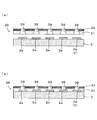
次に、シート36と基板体3を一体化する。図9(a)に示すように、ビアランド2aを有する基板体3の上面とシート36の樹脂層31側を対向配置して、シート36に形成されたビア導体用孔39が、基板体3上面の配線パターン2の所定のビアランド2aの位置に対応するように位置合わせを行う。
その後、図9(b)に示すように、樹脂層31を基板体3の上面に当接して70~130℃で加熱、加圧し、基板体3と樹脂層31を圧着する。このとき、樹脂層31は未硬化であるため、同図(b)に示すように、基板体3の上面に形成されたビアランド2aは樹脂層31に埋設される。また、一体化した基板体3と樹脂層31の上面には、銅箔33が位置することとなる。
次に、図10(a)、(b)に示すように、ビア導体用孔39に導電性ペースト20を充填し、ビア導体32を形成する。導電性ペースト20の充填は、第1実施形態と同様スクリーン印刷方法により行う。なお、導電性ペースト20は、具体的には導電材料(金属)を混入した樹脂ペーストである。
スクリーン印刷方法による導電性ペースト20の充填は、一般的に、スキージが貫通孔を有する層の上面を加圧しながら水平移動するため、上面の剛性が低い場合には、ビア導体用孔や層の形状が変形するおそれがある。例えば、第1実施形態のPETフィルム17上をスキージ21が水平移動するとき、樹脂層4が未硬化であれば、導電性ペースト20の充填時に、PETフィルム17がスキージ21の移動方向にずれ易く、ビア導体15の形状が変形するおそれがある。
これに対して、本実施形態では、上記したように銅箔33が樹脂層31の上面に位置するため、図10(a)に示すように、スキージ21は銅箔33上面を水平方向(図10(a)中の矢印方向)に移動しても、銅箔33が第1実施形態のPETフィルム17よりも剛性が高いことから、銅箔33がスキージ21の方向にずれることはない。
したがって、銅箔33の上面をスキージ21が移動する場合は、樹脂層31が未硬化であっても、ビア導体32がスキージ21の移動方向に変形することがなく、対応するビアランド2aの位置から大きくずれることがない。よって、位置精度の優れたビア導体32を形成することができる。
上記したようにビア導体用孔39に導電性ペースト20を充填してビア導体32を形成した後、シート36および基板体3を180~200℃で加熱する。これにより、樹脂層31と導電性ペースト20が硬化され、同時に樹脂層31に仮圧着された銅箔33も樹脂層31に接着される。
そして、銅箔33の上面を研磨して、ビア導体32と銅箔33を平坦化する。
その後、図11(a)に示すように、銅箔33の上面に導電層34を形成する。導電層34は、銅又は銅合金その他の導電性金属を、電解めっき、無電解めっきにより、ビア導体32および銅箔33を被覆して形成する。
さらに、図11(b)に示すように、銅箔33と導電層34を例えばフォトリソグラフィ、エッチングにより同時にパターンに加工して、複数のビアランド35aを含む配線パターン層35を形成する。したがって、それぞれのビアランド35aは、銅箔33を加工したビアランド33aと導電層34を加工したビアランド34aからなる。また、配線パターン2、ビア導体32、配線パターン層35は電気的に接続されている。
また、図11(b)に示すように、ビア導体32の上面および側面が、それぞれ導電層34を加工したビアランド34aと銅箔33を加工したビアランド33aで覆われているため、ビア導体32に充填された導電性ペースト20が露出することがなく、導電性ペースト20と導電層34が直接接触して精度よく導通する。また、ビア導体32と配線パターン層35の接触面積が大きいため、導通抵抗が低減する。
また、上記した銅箔33は、銅箔に限らず、銅合金やその他の金属箔であってもよい。
このように、第2実施形態によれば、基板体3上にシート36を圧着した後、シート36のビア導体用孔39に導電性ペースト20を充填するので、基板体3と樹脂層31とが密着し、導電性ペースト20が基板体3と樹脂層31との界面に流入するのを防止することができる。したがって、従来のように基板体3と樹脂層31との界面に導電性ペースト20が流入することによる配線パターンの短絡が発生することはなく、より信頼性の優れた樹脂基板を得ることができる。
また、第2実施形態によれば、銅箔33が圧着された状態の樹脂層31にビア導体用孔39を形成した後、ビア導体用孔39に導電性ペースト20を充填するため、銅箔33の剛性によって導電性ペースト20を充填するときのビア導体32の変形を防止することができる。したがって、ビアランド2a、ビア導体32、ビアランド35aの位置精度を向上することができる。
さらに、ビア導体32を導電層34により被覆するため、ビア導体32と導電層34が精度よく導通し、より信頼性の高い配線パターンを形成することができる。また、ビア導体32の側面が銅箔33により覆われるため、ビア導体32と配線パターン層35との接触面積が増加し、導通抵抗を低減することができる。したがって、信頼性の一層優れた樹脂基板を提供することができる。
なお、本発明は上記した実施形態に限定されるものではなく、その趣旨を逸脱しない限りにおいて、上記したもの以外に種々の変更を行うことが可能である。
例えば、上記した実施形態では、スクリーン印刷方法によってビア導体用孔18、39に導電性ペースト20の充填を行っているが、その他の方法によって行ってもよい。
また、上記した実施形態では、炭酸ガスレーザーの照射により貫通孔を形成しているが、その他のレーザーを使用してもよい。また、レーザーの照射に限らず、その他の方法により貫通孔を形成してもよい。
また、基板体3、樹脂層4、31、銅箔23、33、導電層34、導電性ペースト20の構成や材料等は、上記した実施形態に記載したものに限られず、それらの形状や寸法等もどのようなものであってもよい。
本発明は、少なくとも一層の樹脂層を有し、樹脂層に形成された貫通孔に充填された導電性ペーストにより上下両面に形成された配線パターンを電気的に接続した樹脂基板の製造方法および樹脂基板に適用することができ、樹脂基板は樹脂層を複数有するものや、樹脂層に部品が内蔵された部品内蔵基板であってもよい。
Claims (8)
- 上面にビアランドを有する基板体を用意する第1の工程と、
前記ビアランドと対応する位置に貫通孔が形成された樹脂層を前記基板体上に形成する第2の工程と、
前記貫通孔に、導電性ペーストを充填する第3の工程と、
前記樹脂層上面に前記導電性ペーストと電気的に接続された配線パターンを形成する第4の工程と
を備えることを特徴とする樹脂基板の製造方法。 - 前記第4の工程は、未硬化状態の前記樹脂層に金属箔を圧着して前記樹脂層を硬化し、前記金属箔を加工することにより前記配線パターンを形成する工程を含むことを特徴とする請求項1に記載の樹脂基板の製造方法。
- 前記第2の工程は、金属箔が貼設された未硬化状態の前記樹脂層に、前記樹脂層側からレーザーを照射して前記樹脂層および前記金属箔を貫通する前記貫通孔を形成した後、前記樹脂層と前記基板体とが対向するように前記樹脂層を前記基板体上に圧着する工程を含み、
前記第4の工程は、前記金属箔を加工して前記配線パターンを形成する工程を含むことを特徴とする請求項1に記載の樹脂基板の製造方法。 - 前記第4の工程は、前記金属箔上に前記導電性ペーストを被覆する導電層を形成する工程と、前記金属箔と前記導電層を同時に加工する工程とを含むことを特徴とする請求項3に記載の樹脂基板の製造方法。
- 前記第3の工程は、前記導電性ペーストを印刷により充填することを特徴とする請求項1ないし4のいずれかに記載の樹脂基板の製造方法。
- 前記第3の工程の後に、前記樹脂層と前記導電性ペーストを同時に硬化する工程を備えることを特徴とする請求項1ないし5のいずれかに記載の樹脂基板の製造方法。
- 上面にビアランドを有する基板体と、
前記基板体上に形成された樹脂層と、
未硬化状態の前記樹脂層に貼設された金属箔と、
前記樹脂層側からレーザーを照射することにより前記ビアランドと対応する位置の前記樹脂層および前記金属箔を貫通して形成された貫通孔と、
前記貫通孔に充填された導電性ペーストと、
前記樹脂層上面の、前記金属箔を加工して形成され前記導電性ペーストと電気的に接続された配線パターンとを備えることを特徴とする樹脂基板。 - 前記配線パターンに代えて、前記金属箔上に前記導電性ペーストを被覆して形成された導電層と前記金属箔とを同時に加工して前記導電性ペーストと電気的に接続された配線パターンを備えることを特徴とする請求項7に記載の樹脂基板。
Applications Claiming Priority (2)
| Application Number | Priority Date | Filing Date | Title |
|---|---|---|---|
| JP2008064469 | 2008-03-13 | ||
| JP2008-064469 | 2008-03-13 |
Publications (1)
| Publication Number | Publication Date |
|---|---|
| WO2009113602A1 true WO2009113602A1 (ja) | 2009-09-17 |
Family
ID=41065263
Family Applications (1)
| Application Number | Title | Priority Date | Filing Date |
|---|---|---|---|
| PCT/JP2009/054715 Ceased WO2009113602A1 (ja) | 2008-03-13 | 2009-03-12 | 樹脂基板の製造方法および樹脂基板 |
Country Status (1)
| Country | Link |
|---|---|
| WO (1) | WO2009113602A1 (ja) |
Citations (5)
| Publication number | Priority date | Publication date | Assignee | Title |
|---|---|---|---|---|
| JPS6021598A (ja) * | 1983-07-15 | 1985-02-02 | 松下電工株式会社 | 多層配線基板の製造方法 |
| JPH07221450A (ja) * | 1994-02-01 | 1995-08-18 | Hitachi Chem Co Ltd | 多層配線板の製造法 |
| JP2000315863A (ja) * | 1999-04-30 | 2000-11-14 | Toppan Printing Co Ltd | 多層プリント配線板の製造方法 |
| JP2002280741A (ja) * | 2001-03-16 | 2002-09-27 | Hitachi Chem Co Ltd | 多層プリント配線板とその製造法 |
| JP2003136265A (ja) * | 2001-10-26 | 2003-05-14 | Matsushita Electric Ind Co Ltd | レーザ加工方法およびレーザ加工装置と電子デバイス |
-
2009
- 2009-03-12 WO PCT/JP2009/054715 patent/WO2009113602A1/ja not_active Ceased
Patent Citations (5)
| Publication number | Priority date | Publication date | Assignee | Title |
|---|---|---|---|---|
| JPS6021598A (ja) * | 1983-07-15 | 1985-02-02 | 松下電工株式会社 | 多層配線基板の製造方法 |
| JPH07221450A (ja) * | 1994-02-01 | 1995-08-18 | Hitachi Chem Co Ltd | 多層配線板の製造法 |
| JP2000315863A (ja) * | 1999-04-30 | 2000-11-14 | Toppan Printing Co Ltd | 多層プリント配線板の製造方法 |
| JP2002280741A (ja) * | 2001-03-16 | 2002-09-27 | Hitachi Chem Co Ltd | 多層プリント配線板とその製造法 |
| JP2003136265A (ja) * | 2001-10-26 | 2003-05-14 | Matsushita Electric Ind Co Ltd | レーザ加工方法およびレーザ加工装置と電子デバイス |
Similar Documents
| Publication | Publication Date | Title |
|---|---|---|
| JP4291279B2 (ja) | 可撓性多層回路基板 | |
| US8941016B2 (en) | Laminated wiring board and manufacturing method for same | |
| JP4434315B2 (ja) | 多層配線基板の製造方法 | |
| KR101868680B1 (ko) | 회로 기판, 회로 기판의 제조 방법 및 전자 기기 | |
| JPWO2008155957A1 (ja) | 部品内蔵基板の製造方法および部品内蔵基板 | |
| JP2007165888A (ja) | 電子素子内蔵印刷回路基板及びその製造方法 | |
| TWI479972B (zh) | Multi - layer flexible printed wiring board and manufacturing method thereof | |
| JP2012079994A (ja) | 部品内蔵プリント配線板およびその製造方法 | |
| WO2004016054A1 (ja) | 配線基板および配線基板の接続構造 | |
| JP2001332866A (ja) | 回路基板及びその製造方法 | |
| WO2010103695A1 (ja) | 部品内蔵モジュールの製造方法及び部品内蔵モジュール | |
| JP4939519B2 (ja) | 多層回路基板の製造方法 | |
| JP6058321B2 (ja) | 配線基板の製造方法 | |
| KR102052761B1 (ko) | 칩 내장 기판 및 그 제조 방법 | |
| KR100657410B1 (ko) | 다층 인쇄회로기판 제조방법 | |
| JP5671857B2 (ja) | 埋め込み部品具有配線板の製造方法 | |
| WO2009113602A1 (ja) | 樹脂基板の製造方法および樹脂基板 | |
| JP4899409B2 (ja) | 多層プリント配線基板及びその製造方法 | |
| JP5926898B2 (ja) | 配線基板の製造方法 | |
| JP5672675B2 (ja) | 樹脂多層基板 | |
| KR100657406B1 (ko) | 다층 인쇄회로기판 제조방법 | |
| JP2007258736A (ja) | 配線板の製造方法、配線板 | |
| JP2010040906A (ja) | 部品内蔵基板の製造方法および部品内蔵基板 | |
| JP6259054B2 (ja) | 配線基板の製造方法 | |
| JP6062872B2 (ja) | 配線基板 |
Legal Events
| Date | Code | Title | Description |
|---|---|---|---|
| 121 | Ep: the epo has been informed by wipo that ep was designated in this application |
Ref document number: 09720823 Country of ref document: EP Kind code of ref document: A1 |
|
| NENP | Non-entry into the national phase |
Ref country code: DE |
|
| 122 | Ep: pct application non-entry in european phase |
Ref document number: 09720823 Country of ref document: EP Kind code of ref document: A1 |
|
| NENP | Non-entry into the national phase |
Ref country code: JP |